Embed Size (px)
Citation preview
1590 IEEE TRANSACTIONS ON VERY LARGE SCALE INTEGRATION (VLSI) SYSTEMS, VOL. 18, NO. 11, NOVEMBER 2010
Yield-Driven Near-Threshold SRAM DesignGregory Chen, Student Member, IEEE, Dennis Sylvester, Senior Member, IEEE,
David Blaauw, Senior Member, IEEE, and Trevor Mudge, Fellow, IEEE
Abstract—Voltage scaling is desirable in static RAM (SRAM) toreduce energy consumption. However, commercial SRAM is sus-ceptible to functional failures when �� is scaled down. Althoughseveral published SRAM designs scale �� to 200–300 mV, thesedesigns do not sufficiently consider SRAM robustness, limitingthem to small arrays because of yield constraints, and may notcorrectly target the minimum energy operation point. We examinethe effects on area and energy for the differential 6T and 8T bitcells as �� is scaled down, and the bit cells are either sized anddoped, or assisted appropriately to maintain the same yield aswith full ��. SRAM robustness is calculated using importancesampling, resulting in a seven-order run-time improvement overMonte Carlo sampling. Scaling 6T and 8T SRAM �� down to500 mV and scaling 8T SRAM to 300 mV results in a 50% and83% dynamic energy reduction, respectively, with no reductionin robustness and low area overhead, but increased leakage perbit. Using this information, we calculate the supply voltage for aminimum total energy operation � ���� based on activity factorand find that it is significantly higher for SRAM than for logic.
Index Terms—Low power, near threshold, robustness, staticRAM (SRAM), threshold voltage tuning.
I. INTRODUCTION
R EDUCTION of energy consumption is desirable in mi-croprocessors to enable longer battery life and adequate
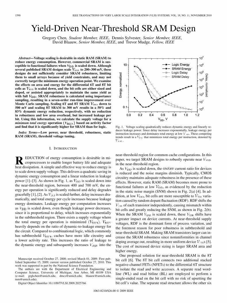
heat dissipation. A simple and effective way to reduce energy isto scale down supply voltage. This delivers a quadratic saving indynamic energy consumption and a linear reduction in leakagepower [1]–[3]. As shown in Fig. 1, as is scaled down intothe near-threshold region, between 400 and 700 mV, the en-ergy per operation is significantly reduced and delay degradesgracefully [1], [2]. As is scaled further, delay increases dra-matically, and total energy per cycle increases because leakageenergy dominates. Leakage energy per computation increasesas is scaled down, even though leakage power decreases,since it is proportional to delay, which increases exponentiallyin the subthreshold region. There exists a supply voltage wherethe total energy per operation is minimized .heavily depends on the ratio of dynamic-to-leakage energy forthe circuit. Compared to combinational logic, which commonlyhas subthreshold , caches have more idle circuitry anda lower activity rate. This increases the ratio of leakage tothe dynamic energy and subsequently increases into the
Manuscript received October 27, 2008; revised March 01, 2009. First pub-lished September 15, 2009; current version published October 27, 2010. Thiswork was supported in part by the National Science Foundation.
The authors are with the Department of Electrical Engineering andComputer Science, University of Michigan, Ann Arbor, MI 48109 USA(e-mail: [email protected]; [email protected]; [email protected];[email protected]).
Digital Object Identifier 10.1109/TVLSI.2009.2025766
Fig. 1. Voltage scaling quadratically reduces dynamic energy and linearly re-duces leakage power. Since delay increases exponentially, leakage energy perinstruction increases and dominates total energy at low � . These competingtrends result in a � that minimizes total energy per instruction, denoted by� .
near-threshold region for common cache configurations. In thispaper, we target SRAM designs to robustly operate nearin the near-threshold region.
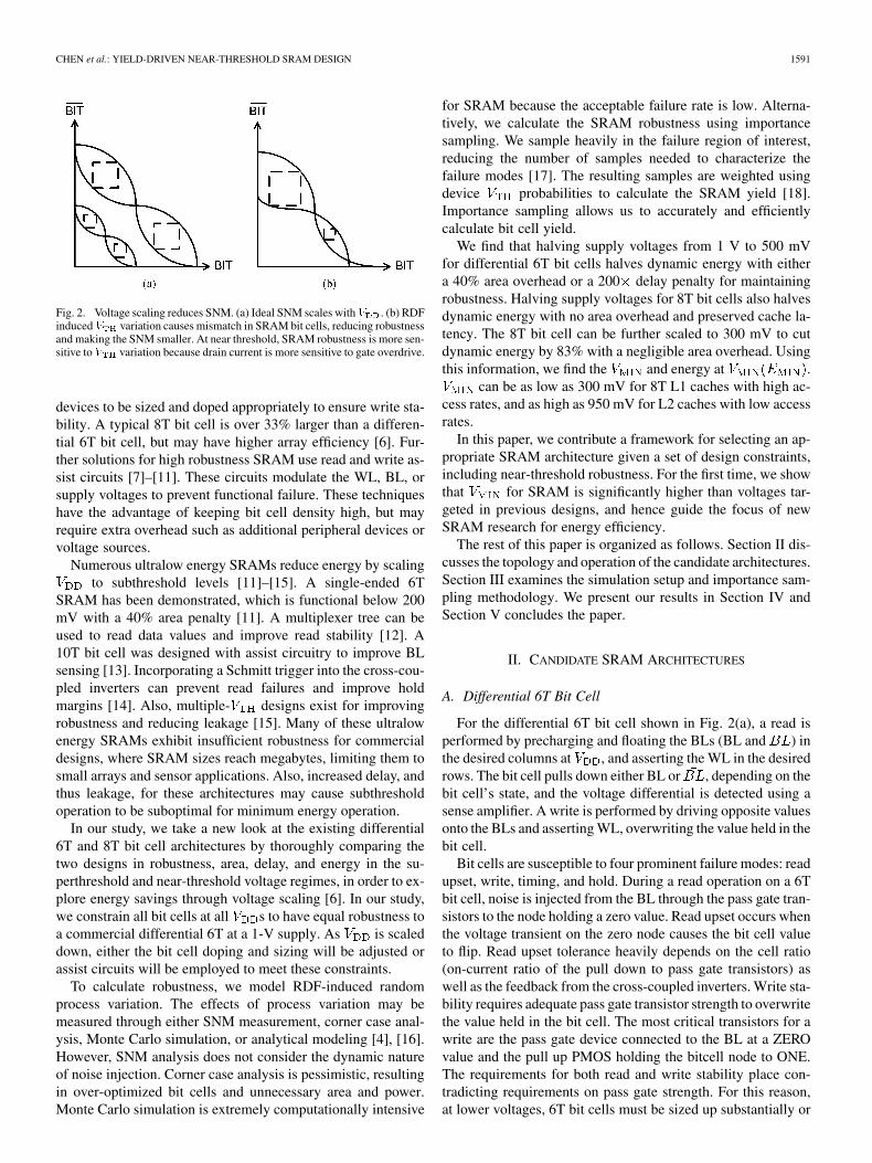
As is scaled down, the ON/OFF current ratio for devicesis reduced and the noise margins diminish. Typically, CMOScircuitry maintains adequate robustness in the presence of theseeffects. However, static RAM (SRAM) becomes more prone tofunctional failures at low , as evidenced by the reductionin the static noise margin (SNM) shown in Fig. 2(a) [4]. In ad-dition, at low , bit cells are more susceptible to varia-tion caused by random dopant fluctuation (RDF). RDF shifts the
of each transistor independently, causing mismatch withinbit cells and greatly reducing the SNM, as shown in Fig. 2(b).When the SRAM is scaled down, these shifts havea greater impact on device currents. At near-threshold supplyvoltages, RDF is the dominant form of process variation, andthe foremost reason for poor robustness in subthreshold andnear-threshold SRAM. Making SRAM transistors larger can in-crease the SRAM robustness since nonuniformities in channeldoping average out, resulting in more uniform device s [5].The cost of increased device sizing is larger SRAM area andhigher energy.
One proposed solution for near-threshold SRAM is the 8Tbit cell [6]. The 8T bit cell connects two additional stackednegative-channel FETs (NFETs) to the differential 6T structureto isolate the read and write accesses. A separate read word-line (WL) and read bitline (BL) are employed to perform asingle-ended read on the bit cell with no risk of upsetting thebit cell’s value. The separate read structure allows the other six
1063-8210/$26.00 © 2009 IEEE
CHEN et al.: YIELD-DRIVEN NEAR-THRESHOLD SRAM DESIGN 1591
Fig. 2. Voltage scaling reduces SNM. (a) Ideal SNM scales with � . (b) RDFinduced � variation causes mismatch in SRAM bit cells, reducing robustnessand making the SNM smaller. At near threshold, SRAM robustness is more sen-sitive to � variation because drain current is more sensitive to gate overdrive.
devices to be sized and doped appropriately to ensure write sta-bility. A typical 8T bit cell is over 33% larger than a differen-tial 6T bit cell, but may have higher array efficiency [6]. Fur-ther solutions for high robustness SRAM use read and write as-sist circuits [7]–[11]. These circuits modulate the WL, BL, orsupply voltages to prevent functional failure. These techniqueshave the advantage of keeping bit cell density high, but mayrequire extra overhead such as additional peripheral devices orvoltage sources.
Numerous ultralow energy SRAMs reduce energy by scalingto subthreshold levels [11]–[15]. A single-ended 6T
SRAM has been demonstrated, which is functional below 200mV with a 40% area penalty [11]. A multiplexer tree can beused to read data values and improve read stability [12]. A10T bit cell was designed with assist circuitry to improve BLsensing [13]. Incorporating a Schmitt trigger into the cross-cou-pled inverters can prevent read failures and improve holdmargins [14]. Also, multiple- designs exist for improvingrobustness and reducing leakage [15]. Many of these ultralowenergy SRAMs exhibit insufficient robustness for commercialdesigns, where SRAM sizes reach megabytes, limiting them tosmall arrays and sensor applications. Also, increased delay, andthus leakage, for these architectures may cause subthresholdoperation to be suboptimal for minimum energy operation.
In our study, we take a new look at the existing differential6T and 8T bit cell architectures by thoroughly comparing thetwo designs in robustness, area, delay, and energy in the su-perthreshold and near-threshold voltage regimes, in order to ex-plore energy savings through voltage scaling [6]. In our study,we constrain all bit cells at all s to have equal robustness toa commercial differential 6T at a 1-V supply. As is scaleddown, either the bit cell doping and sizing will be adjusted orassist circuits will be employed to meet these constraints.
To calculate robustness, we model RDF-induced randomprocess variation. The effects of process variation may bemeasured through either SNM measurement, corner case anal-ysis, Monte Carlo simulation, or analytical modeling [4], [16].However, SNM analysis does not consider the dynamic natureof noise injection. Corner case analysis is pessimistic, resultingin over-optimized bit cells and unnecessary area and power.Monte Carlo simulation is extremely computationally intensive
for SRAM because the acceptable failure rate is low. Alterna-tively, we calculate the SRAM robustness using importancesampling. We sample heavily in the failure region of interest,reducing the number of samples needed to characterize thefailure modes [17]. The resulting samples are weighted usingdevice probabilities to calculate the SRAM yield [18].Importance sampling allows us to accurately and efficientlycalculate bit cell yield.
We find that halving supply voltages from 1 V to 500 mVfor differential 6T bit cells halves dynamic energy with eithera 40% area overhead or a 200 delay penalty for maintainingrobustness. Halving supply voltages for 8T bit cells also halvesdynamic energy with no area overhead and preserved cache la-tency. The 8T bit cell can be further scaled to 300 mV to cutdynamic energy by 83% with a negligible area overhead. Usingthis information, we find the and energy at .
can be as low as 300 mV for 8T L1 caches with high ac-cess rates, and as high as 950 mV for L2 caches with low accessrates.
In this paper, we contribute a framework for selecting an ap-propriate SRAM architecture given a set of design constraints,including near-threshold robustness. For the first time, we showthat for SRAM is significantly higher than voltages tar-geted in previous designs, and hence guide the focus of newSRAM research for energy efficiency.
The rest of this paper is organized as follows. Section II dis-cusses the topology and operation of the candidate architectures.Section III examines the simulation setup and importance sam-pling methodology. We present our results in Section IV andSection V concludes the paper.
II. CANDIDATE SRAM ARCHITECTURES
A. Differential 6T Bit Cell
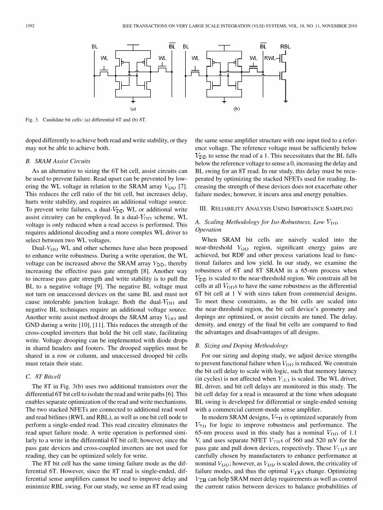
For the differential 6T bit cell shown in Fig. 2(a), a read isperformed by precharging and floating the BLs (BL and ) inthe desired columns at , and asserting the WL in the desiredrows. The bit cell pulls down either BL or , depending on thebit cell’s state, and the voltage differential is detected using asense amplifier. A write is performed by driving opposite valuesonto the BLs and asserting WL, overwriting the value held in thebit cell.
Bit cells are susceptible to four prominent failure modes: readupset, write, timing, and hold. During a read operation on a 6Tbit cell, noise is injected from the BL through the pass gate tran-sistors to the node holding a zero value. Read upset occurs whenthe voltage transient on the zero node causes the bit cell valueto flip. Read upset tolerance heavily depends on the cell ratio(on-current ratio of the pull down to pass gate transistors) aswell as the feedback from the cross-coupled inverters. Write sta-bility requires adequate pass gate transistor strength to overwritethe value held in the bit cell. The most critical transistors for awrite are the pass gate device connected to the BL at a ZEROvalue and the pull up PMOS holding the bitcell node to ONE.The requirements for both read and write stability place con-tradicting requirements on pass gate strength. For this reason,at lower voltages, 6T bit cells must be sized up substantially or
1592 IEEE TRANSACTIONS ON VERY LARGE SCALE INTEGRATION (VLSI) SYSTEMS, VOL. 18, NO. 11, NOVEMBER 2010
Fig. 3. Candidate bit cells: (a) differential 6T and (b) 8T.
doped differently to achieve both read and write stability, or theymay not be able to achieve both.
B. SRAM Assist Circuits
As an alternative to sizing the 6T bit cell, assist circuits canbe used to prevent failure. Read upset can be prevented by low-ering the WL voltage in relation to the SRAM array [7].This reduces the cell ratio of the bit cell, but increases delay,hurts write stability, and requires an additional voltage source.To prevent write failures, a dual- WL or additional writeassist circuitry can be employed. In a dual- scheme, WLvoltage is only reduced when a read access is performed. Thisrequires additional decoding and a more complex WL driver toselect between two WL voltages.
Dual- WL and other schemes have also been proposedto enhance write robustness. During a write operation, the WLvoltage can be increased above the SRAM array , therebyincreasing the effective pass gate strength [8]. Another wayto increase pass gate strength and write stability is to pull theBL to a negative voltage [9]. The negative BL voltage mustnot turn on unaccessed devices on the same BL and must notcause intolerable junction leakage. Both the dual- andnegative BL techniques require an additional voltage source.Another write assist method droops the SRAM array andGND during a write [10], [11]. This reduces the strength of thecross-coupled inverters that hold the bit cell state, facilitatingwrite. Voltage drooping can be implemented with diode dropsin shared headers and footers. The drooped supplies must beshared in a row or column, and unaccessed drooped bit cellsmust retain their state.
C. 8T Bitcell
The 8T in Fig. 3(b) uses two additional transistors over thedifferential 6T bit cell to isolate the read and write paths [6]. Thisenables separate optimization of the read and write mechanisms.The two stacked NFETs are connected to additional read wordand read bitlines (RWL and RBL), as well as one bit cell node toperform a single-ended read. This read circuitry eliminates theread upset failure mode. A write operation is performed simi-larly to a write in the differential 6T bit cell; however, since thepass gate devices and cross-coupled inverters are not used forreading, they can be optimized solely for write.
The 8T bit cell has the same timing failure mode as the dif-ferential 6T. However, since the 8T read is single-ended, dif-ferential sense amplifiers cannot be used to improve delay andminimize RBL swing. For our study, we sense an 8T read using
the same sense amplifier structure with one input tied to a refer-ence voltage. The reference voltage must be sufficiently below
to sense the read of a 1. This necessitates that the BL fallsbelow the reference voltage to sense a 0, increasing the delay andBL swing for an 8T read. In our study, this delay must be recu-perated by optimizing the stacked NFETs used for reading. In-creasing the strength of these devices does not exacerbate otherfailure modes; however, it incurs area and energy penalties.
III. RELIABILITY ANALYSIS USING IMPORTANCE SAMPLING
A. Scaling Methodology for Iso-Robustness, LowOperation
When SRAM bit cells are naively scaled into thenear-threshold region, significant energy gains areachieved, but RDF and other process variations lead to func-tional failures and low yield. In our study, we examine therobustness of 6T and 8T SRAM in a 65-nm process when
is scaled to the near-threshold region. We constrain all bitcells at all s to have the same robustness as the differential6T bit cell at 1 V with sizes taken from commercial designs.To meet these constraints, as the bit cells are scaled intothe near-threshold region, the bit cell device’s geometry anddopings are optimized, or assist circuits are tuned. The delay,density, and energy of the final bit cells are compared to findthe advantages and disadvantages of all designs.
B. Sizing and Doping Methodology
For our sizing and doping study, we adjust device strengthsto prevent functional failure when is reduced. We constrainthe bit cell delay to scale with logic, such that memory latency(in cycles) is not affected when is scaled. The WL driver,BL driver, and bit cell delays are monitored in this study. Thebit cell delay for a read is measured at the time when adequateBL swing is developed for differential or single-ended sensingwith a commercial current-mode sense amplifier.
In modern SRAM designs, is optimized separately fromfor logic to improve robustness and performance. The
65-nm process used in this study has a nominal of 1.1V, and uses separate NFET s of 560 and 520 mV for thepass gate and pull down devices, respectively. These s arecarefully chosen by manufacturers to enhance performance atnominal ; however, as is scaled down, the criticality offailure modes, and thus the optimal s change. Optimizing
can help SRAM meet delay requirements as well as controlthe current ratios between devices to balance probabilities of
CHEN et al.: YIELD-DRIVEN NEAR-THRESHOLD SRAM DESIGN 1593
different failure modes. When is tuned, is calculatedappropriately according to the device models. Circuit designershave limited flexibility to tune ; therefore, in this study,we optimize the device geometry alone and also geometry withindividual device s. Reasonable limits are placed onto ensure realistic doping concentrations and tolerable leakagepower.
C. Assist Circuit Methodology
In our study of assist circuits, we maintain bit cell robust-ness as is scaled down by adjusting the peripheral circuits.Assist circuits are unnecessary for the 8T bitcell because thereis no read upset failure mode, and write stability can be main-tained with minimal sizing. The 6T bitcell design in our studyis taken from a commercial design optimized for superthresholdoperation, and no device sizing or tuning is performed.To maintain read stability, a dual- WL with reduced readvoltage is used. This read assist circuit incurs a delay penalty,precluding isolatency voltage scaling, so there is no delay con-straint for the assist circuit study. For write robustness, threemethods will be compared: overdriven WL, negative BL, andsupply rail drooping. In the latter two cases, the assist circuitsmust be adjusted appropriately not to disturb the unaccessed bitcells. The resulting decrease in bit cell performance and changesin energy consumption are measured.
D. Robustness Calculation Using Importance Sampling
At this point, an accurate metric of SRAM robustness is nec-essary to determine when optimization is complete. SRAM ro-bustness is often measured using SNM because it is relativelyeasy to compute. However, SNM does not consider the dynamicnature of noise injection into bit cells. Since the probability ofinjecting the same amount of noise changes as is scaled,SNM does not translate directly to SRAM yield. Corner casescan also be used to measure robustness; however, in general, thesupplied corner cases only consider global variation and not de-vice mismatch. Since mismatch has a strong effect on the SRAMyield, these cases are not sufficient. Corner cases involving mis-match can be performed, but have several drawbacks. First, dif-ferent transistors have differing criticality for SRAM function-ality, but in corner case analysis the same amount of variation isplaced on each device, making the analysis incomplete. Second,calculating the SRAM yield based on corner case simulations isnontrivial.
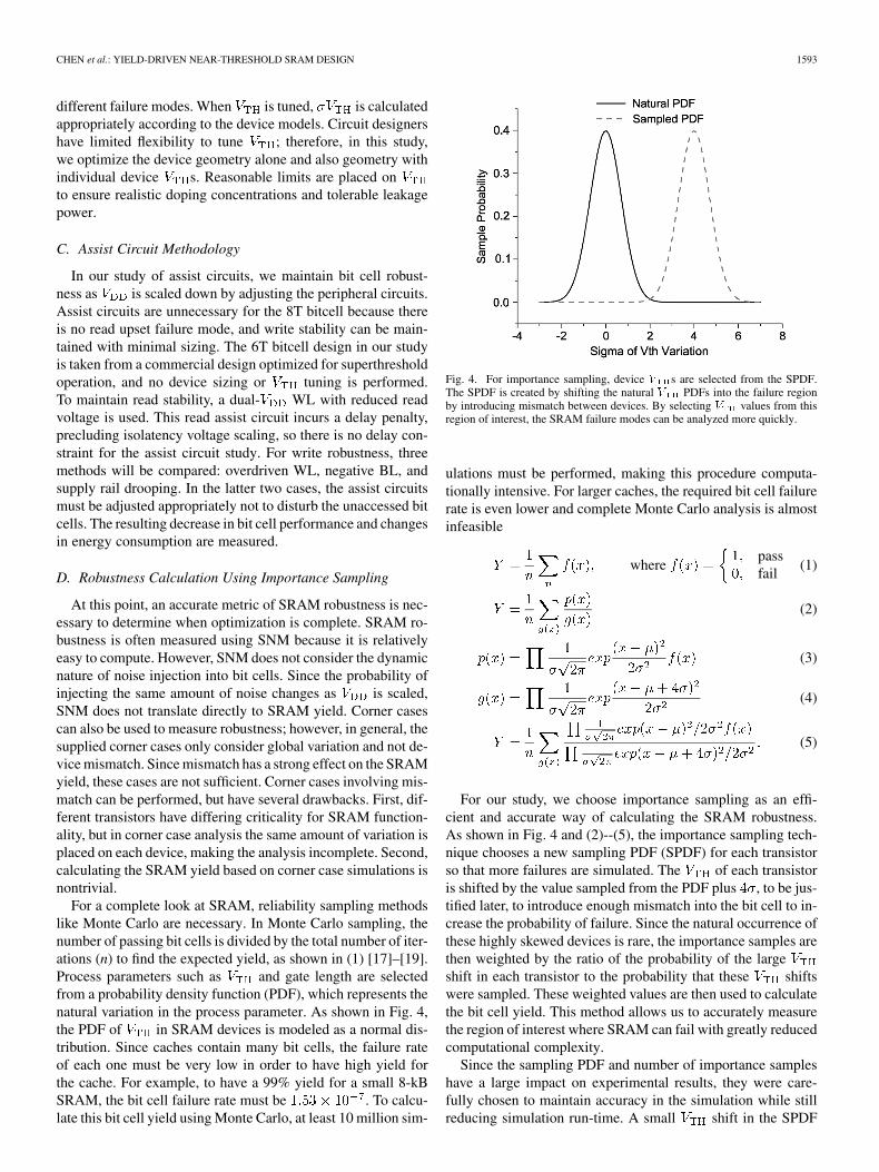
For a complete look at SRAM, reliability sampling methodslike Monte Carlo are necessary. In Monte Carlo sampling, thenumber of passing bit cells is divided by the total number of iter-ations (n) to find the expected yield, as shown in (1) [17]–[19].Process parameters such as and gate length are selectedfrom a probability density function (PDF), which represents thenatural variation in the process parameter. As shown in Fig. 4,the PDF of in SRAM devices is modeled as a normal dis-tribution. Since caches contain many bit cells, the failure rateof each one must be very low in order to have high yield forthe cache. For example, to have a 99% yield for a small 8-kBSRAM, the bit cell failure rate must be . To calcu-late this bit cell yield using Monte Carlo, at least 10 million sim-
Fig. 4. For importance sampling, device � s are selected from the SPDF.The SPDF is created by shifting the natural � PDFs into the failure regionby introducing mismatch between devices. By selecting � values from thisregion of interest, the SRAM failure modes can be analyzed more quickly.
ulations must be performed, making this procedure computa-tionally intensive. For larger caches, the required bit cell failurerate is even lower and complete Monte Carlo analysis is almostinfeasible
wherepassfail
(1)
(2)
(3)
(4)
(5)
For our study, we choose importance sampling as an effi-cient and accurate way of calculating the SRAM robustness.As shown in Fig. 4 and (2)--(5), the importance sampling tech-nique chooses a new sampling PDF (SPDF) for each transistorso that more failures are simulated. The of each transistoris shifted by the value sampled from the PDF plus , to be jus-tified later, to introduce enough mismatch into the bit cell to in-crease the probability of failure. Since the natural occurrence ofthese highly skewed devices is rare, the importance samples arethen weighted by the ratio of the probability of the largeshift in each transistor to the probability that these shiftswere sampled. These weighted values are then used to calculatethe bit cell yield. This method allows us to accurately measurethe region of interest where SRAM can fail with greatly reducedcomputational complexity.
Since the sampling PDF and number of importance sampleshave a large impact on experimental results, they were care-fully chosen to maintain accuracy in the simulation while stillreducing simulation run-time. A small shift in the SPDF
1594 IEEE TRANSACTIONS ON VERY LARGE SCALE INTEGRATION (VLSI) SYSTEMS, VOL. 18, NO. 11, NOVEMBER 2010
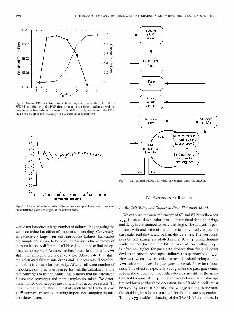
Fig. 5. Natural PDF is shifted into the failure region to create the SPDF. If theSPDF is too similar to the PDF, then simulation run-time to calculate yield islong because few failures are seen. If the SPDF greatly varies from the PDF,then more samples are necessary for accurate yield calculations.
Fig. 6. After a sufficient number of importance samples have been simulated,the calculated yield converges to the correct value.
would not introduce a large number of failures, thus negating thevariance reduction effect of importance sampling. Conversely,an excessively large shift introduces failures, but causesthe sample weighting to be small and reduces the accuracy ofthe simulation. A differential 6T bit cell is studied to find the op-timal sampling PDF. As shown in Fig. 5, with less than ashift, the sample failure rate is very low. Above a shift,the calculated failure rate drops and is inaccurate. Therefore,a shift is chosen for our study. After a sufficient number ofimportance samples have been performed, the calculated failurerate converges to its final value. Fig. 6 shows that the calculatedfailure rate converges and more samples are taken. We deter-mine that 20 000 samples are sufficient for accurate results. Tomeasure the failure rates in our study with Monte Carlo, at least
samples are needed, making importance sampling 50 mil-lion times faster.
Fig. 7. Design methodology for yield-driven near-threshold SRAM.
IV. EXPERIMENTAL RESULTS
A. Bit Cell Sizing and Doping in Near-Threshold SRAM
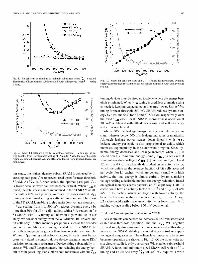
We examine the area and energy of 6T and 8T bit cells whenis scaled down, robustness is maintained through sizing,
and delay is constrained to scale with logic. The analysis is per-formed with and without the ability to individually adjust thepass gate, pull down, and pull up device s. The isorobust-ness bit cell sizings are plotted in Fig. 8. tuning dramat-ically reduces the required bit cell area at low voltage.is often set higher for pass gate devices than for pull downdevices to prevent read upset failures at superthreshold .However, when is scaled to near-threshold voltages, this
selection makes the pass gates too weak for write robust-ness. This effect is especially strong when the pass gates entersubthreshold operation, but other devices are still in the near-threshold regime. If is a fixed parameter set as a value op-timized for superthreshold operation, then SRAM bit cells mustbe sized by 400% at 500 mV, and voltage scaling to the sub-threshold regions is not practical for isorobustness operation.Tuning enables balancing of the SRAM failure modes. In
CHEN et al.: YIELD-DRIVEN NEAR-THRESHOLD SRAM DESIGN 1595
Fig. 8. Bit cells can be sized up to maintain robustness when � is scaled.The density of isorobustness subthreshold SRAM is improved when� tuningis used.
Fig. 9. When bit cells are sized for robustness without � tuning, the en-ergy benefits from isorobustness scaling of 65-nm SRAM to the near-thresholdregion are limited because WL and BL capacitances from upsized devices areprohibitive.
our study, the highest density, robust SRAM is achieved by in-creasing pass gate to prevent read upset for near-thresholdSRAM. As is further scaled, the optimal pass gateis lower because write failures become critical. When istuned, the robustness can be maintained in the 6T SRAM at 500mV with a 40% area penalty. Across all voltages studied,tuning with minimal sizing is sufficient to maintain robustnessin the 8T SRAM, enabling high-density low-voltage memory.
scaling from 1 to 500 mV reduces dynamic energy bymore than 50% for all bit cells studied, with a 61% reduction for8T SRAM with tuning, as shown in Figs. 9 and 10. In ourstudy, we consider energy from the WL drivers, BL drivers, andbit cells only. If other memory peripheries, such as the decoderand sense amplifiers, are voltage scaled with the SRAM bitcells, then energy gains greater than those reported are possible.Without tuning and at low voltages, bit cells must be ag-gressively sized to control relative device strengths under RDFvariation to maintain robustness. Device sizing substantially in-creases WL and BL capacitances, thus reducing the energy ben-efit of voltage scaling. For subthreshold robustness without
Fig. 10. When bit cells are sized and � is tuned for robustness, dynamicenergy can be reduced by as much as 83% in isorobustness SRAM using voltagescaling.
tuning, devices must be sized up to a level where the energy ben-efit is eliminated. When tuning is used, less dramatic sizingis needed, keeping capacitance and energy lower. Usingtuning for near-threshold 550-mV SRAM reduces dynamic en-ergy by 44% and 56% for 6T and 8T SRAMs, respectively, overthe fixed case. For 8T SRAM, isorobustness operation at300 mV is obtained with little device sizing, and an 83% energyreduction is achieved.
Above 500 mV, leakage energy per cycle is relatively con-stant, whereas below 500 mV, leakage increases dramatically.Although leakage power scales down linearly with ,leakage energy per cycle is also proportional to delay, whichincreases exponentially in the subthreshold region. Since dy-namic energy decreases and leakage increases when isscaled down, a minimum energy point is achieved atsome intermediate voltage [1]. As seen in Figs. 11 and12, and are heavily dependent on the activity factor,which we define as the average fraction of bit cells accessedper cycle. For L1 caches, which are generally small with highactivity, the total energy is almost entirely dynamic, makingvoltage scaling a desirable method for energy reduction. Basedon typical memory access patterns, an 8T eight-way 1 kB L1cache could have an activity factor of and a of 450mV. In L2 caches, which are larger with lower activity, thebenefits of voltage scaling are reduced and rises. A largeL2 cache could easily have an activity factor lower than ,making voltage scaling below 850 mV detrimental.
B. Assist Circuits for Near-Threshold SRAM
Assist circuits can be used to increase SRAM robustness andenable near-threshold operation. The dual- WL, negativeBL, and supply drooping assist circuits considered in this studyincrease the SRAM stability by modifying control or supplyvoltages during accesses. The voltage levels necessary for isoro-bustness operation are shown in Fig. 13. Of the three write as-sist circuits studied, only overdriven WL enables subthresholdSRAM. A functional minimum-sized SRAM cell with notuning and an SRAM array of 300 mV requires a write
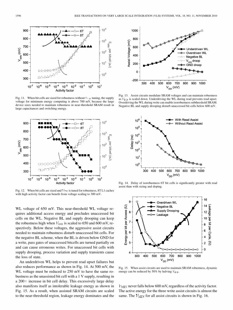
1596 IEEE TRANSACTIONS ON VERY LARGE SCALE INTEGRATION (VLSI) SYSTEMS, VOL. 18, NO. 11, NOVEMBER 2010
Fig. 11. When bit cells are sized for robustness without � tuning, the supplyvoltage for minimum energy computing is above 700 mV, because the largedevice sizes needed to maintain robustness in near-threshold SRAM result inlarge capacitances and switching energy.
Fig. 12. When bit cells are sized and� is tuned for robustness, 8T L1 cacheswith high activity factor can benefit from voltage scaling to 300 mV.
WL voltage of 650 mV. This near-threshold WL voltage re-quires additional access energy and precludes unaccessed bitcells on the WL. Negative BL and supply drooping can keepthe robustness high when is scaled to 650 and 600 mV, re-spectively. Below these voltages, the aggressive assist circuitsneeded to maintain robustness disturb unaccessed bit cells. Forthe negative BL scheme, when the BL is driven below GND fora write, pass gates of unaccessed bitcells are turned partially onand can cause erroneous writes. For unaccessed bit cells withsupply drooping, process variation and supply transients causethe loss of state.
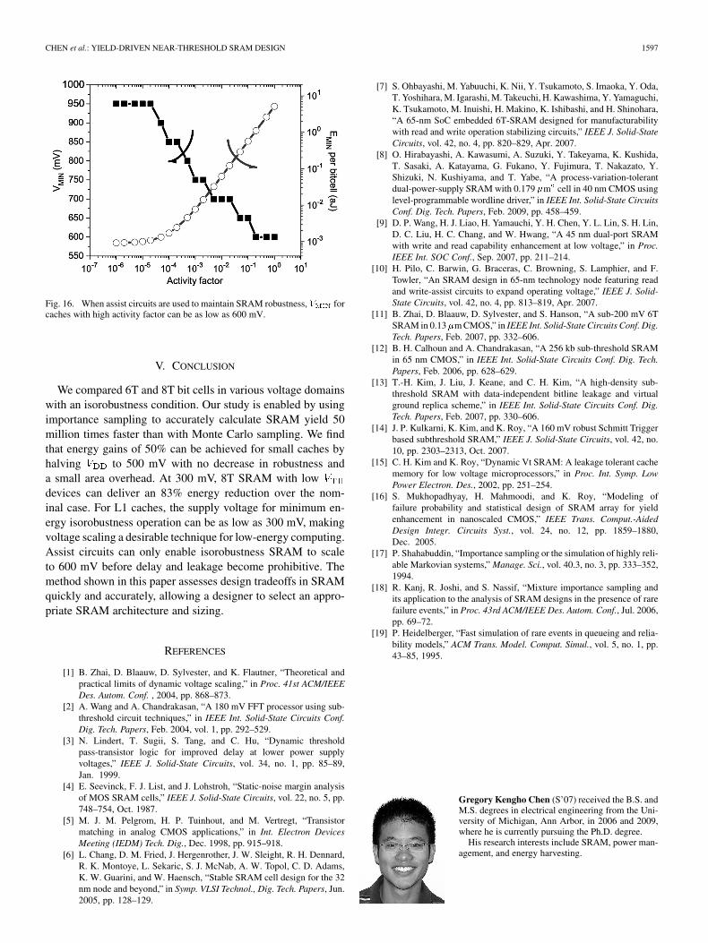
An underdriven WL helps to prevent read upset failures butalso reduces performance as shown in Fig. 14. At 500 mV, theWL voltage must be reduced to 250 mV to have the same ro-bustness as the unassisted bit cell with a 1 V supply, resulting ina 200 increase in bit cell delay. This excessively large delayalso manifests itself as intolerable leakage energy as shown inFig. 15. As a result, when assisted SRAM circuits are scaledto the near-threshold region, leakage energy dominates and the
Fig. 13. Assist circuits modulate SRAM voltages and can maintain robustnessas � is scaled down. Underdriving the WL during read prevents read upset.Overdriving the WL during write can enable isorobustness subthreshold SRAM.Negative BL and supply drooping disturb unaccessed bit cells below 600 mV.
Fig. 14. Delay of isorobustness 6T bit cells is significantly greater with readassist than with sizing and doping.
Fig. 15. When assist circuits are used to maintain SRAM robustness, dynamicenergy can be reduced by 50% by halving � .
never falls below 600 mV, regardless of the activity factor.The active energy for the three write assist circuits is almost thesame. The for all assist circuits is shown in Fig. 16.
CHEN et al.: YIELD-DRIVEN NEAR-THRESHOLD SRAM DESIGN 1597
Fig. 16. When assist circuits are used to maintain SRAM robustness, � forcaches with high activity factor can be as low as 600 mV.
V. CONCLUSION
We compared 6T and 8T bit cells in various voltage domainswith an isorobustness condition. Our study is enabled by usingimportance sampling to accurately calculate SRAM yield 50million times faster than with Monte Carlo sampling. We findthat energy gains of 50% can be achieved for small caches byhalving to 500 mV with no decrease in robustness anda small area overhead. At 300 mV, 8T SRAM with lowdevices can deliver an 83% energy reduction over the nom-inal case. For L1 caches, the supply voltage for minimum en-ergy isorobustness operation can be as low as 300 mV, makingvoltage scaling a desirable technique for low-energy computing.Assist circuits can only enable isorobustness SRAM to scaleto 600 mV before delay and leakage become prohibitive. Themethod shown in this paper assesses design tradeoffs in SRAMquickly and accurately, allowing a designer to select an appro-priate SRAM architecture and sizing.
REFERENCES
[1] B. Zhai, D. Blaauw, D. Sylvester, and K. Flautner, “Theoretical andpractical limits of dynamic voltage scaling,” in Proc. 41st ACM/IEEEDes. Autom. Conf. , 2004, pp. 868–873.
[2] A. Wang and A. Chandrakasan, “A 180 mV FFT processor using sub-threshold circuit techniques,” in IEEE Int. Solid-State Circuits Conf.Dig. Tech. Papers, Feb. 2004, vol. 1, pp. 292–529.
[3] N. Lindert, T. Sugii, S. Tang, and C. Hu, “Dynamic thresholdpass-transistor logic for improved delay at lower power supplyvoltages,” IEEE J. Solid-State Circuits, vol. 34, no. 1, pp. 85–89,Jan. 1999.
[4] E. Seevinck, F. J. List, and J. Lohstroh, “Static-noise margin analysisof MOS SRAM cells,” IEEE J. Solid-State Circuits, vol. 22, no. 5, pp.748–754, Oct. 1987.
[5] M. J. M. Pelgrom, H. P. Tuinhout, and M. Vertregt, “Transistormatching in analog CMOS applications,” in Int. Electron DevicesMeeting (IEDM) Tech. Dig., Dec. 1998, pp. 915–918.
[6] L. Chang, D. M. Fried, J. Hergenrother, J. W. Sleight, R. H. Dennard,R. K. Montoye, L. Sekaric, S. J. McNab, A. W. Topol, C. D. Adams,K. W. Guarini, and W. Haensch, “Stable SRAM cell design for the 32nm node and beyond,” in Symp. VLSI Technol., Dig. Tech. Papers, Jun.2005, pp. 128–129.
[7] S. Ohbayashi, M. Yabuuchi, K. Nii, Y. Tsukamoto, S. Imaoka, Y. Oda,T. Yoshihara, M. Igarashi, M. Takeuchi, H. Kawashima, Y. Yamaguchi,K. Tsukamoto, M. Inuishi, H. Makino, K. Ishibashi, and H. Shinohara,“A 65-nm SoC embedded 6T-SRAM designed for manufacturabilitywith read and write operation stabilizing circuits,” IEEE J. Solid-StateCircuits, vol. 42, no. 4, pp. 820–829, Apr. 2007.
[8] O. Hirabayashi, A. Kawasumi, A. Suzuki, Y. Takeyama, K. Kushida,T. Sasaki, A. Katayama, G. Fukano, Y. Fujimura, T. Nakazato, Y.Shizuki, N. Kushiyama, and T. Yabe, “A process-variation-tolerantdual-power-supply SRAM with 0.179 �m cell in 40 nm CMOS usinglevel-programmable wordline driver,” in IEEE Int. Solid-State CircuitsConf. Dig. Tech. Papers, Feb. 2009, pp. 458–459.
[9] D. P. Wang, H. J. Liao, H. Yamauchi, Y. H. Chen, Y. L. Lin, S. H. Lin,D. C. Liu, H. C. Chang, and W. Hwang, “A 45 nm dual-port SRAMwith write and read capability enhancement at low voltage,” in Proc.IEEE Int. SOC Conf., Sep. 2007, pp. 211–214.
[10] H. Pilo, C. Barwin, G. Braceras, C. Browning, S. Lamphier, and F.Towler, “An SRAM design in 65-nm technology node featuring readand write-assist circuits to expand operating voltage,” IEEE J. Solid-State Circuits, vol. 42, no. 4, pp. 813–819, Apr. 2007.
[11] B. Zhai, D. Blaauw, D. Sylvester, and S. Hanson, “A sub-200 mV 6TSRAM in 0.13�m CMOS,” in IEEE Int. Solid-State Circuits Conf. Dig.Tech. Papers, Feb. 2007, pp. 332–606.
[12] B. H. Calhoun and A. Chandrakasan, “A 256 kb sub-threshold SRAMin 65 nm CMOS,” in IEEE Int. Solid-State Circuits Conf. Dig. Tech.Papers, Feb. 2006, pp. 628–629.
[13] T.-H. Kim, J. Liu, J. Keane, and C. H. Kim, “A high-density sub-threshold SRAM with data-independent bitline leakage and virtualground replica scheme,” in IEEE Int. Solid-State Circuits Conf. Dig.Tech. Papers, Feb. 2007, pp. 330–606.
[14] J. P. Kulkarni, K. Kim, and K. Roy, “A 160 mV robust Schmitt Triggerbased subthreshold SRAM,” IEEE J. Solid-State Circuits, vol. 42, no.10, pp. 2303–2313, Oct. 2007.
[15] C. H. Kim and K. Roy, “Dynamic Vt SRAM: A leakage tolerant cachememory for low voltage microprocessors,” in Proc. Int. Symp. LowPower Electron. Des., 2002, pp. 251–254.
[16] S. Mukhopadhyay, H. Mahmoodi, and K. Roy, “Modeling offailure probability and statistical design of SRAM array for yieldenhancement in nanoscaled CMOS,” IEEE Trans. Comput.-AidedDesign Integr. Circuits Syst., vol. 24, no. 12, pp. 1859–1880,Dec. 2005.
[17] P. Shahabuddin, “Importance sampling or the simulation of highly reli-able Markovian systems,” Manage. Sci., vol. 40.3, no. 3, pp. 333–352,1994.
[18] R. Kanj, R. Joshi, and S. Nassif, “Mixture importance sampling andits application to the analysis of SRAM designs in the presence of rarefailure events,” in Proc. 43rd ACM/IEEE Des. Autom. Conf., Jul. 2006,pp. 69–72.
[19] P. Heidelberger, “Fast simulation of rare events in queueing and relia-bility models,” ACM Trans. Model. Comput. Simul., vol. 5, no. 1, pp.43–85, 1995.
Gregory Kengho Chen (S’07) received the B.S. andM.S. degrees in electrical engineering from the Uni-versity of Michigan, Ann Arbor, in 2006 and 2009,where he is currently pursuing the Ph.D. degree.
His research interests include SRAM, power man-agement, and energy harvesting.
1598 IEEE TRANSACTIONS ON VERY LARGE SCALE INTEGRATION (VLSI) SYSTEMS, VOL. 18, NO. 11, NOVEMBER 2010
Dennis Sylvester (S’95–M’00–SM’04) received thePh.D. degree in electrical engineering from the Uni-versity of California, Berkeley, where his disserta-tion research was recognized by the David J. SakrisonMemorial Prize as the most outstanding research inthe UC-Berkeley EECS Department.
He is currently an Associate Professor with theDepartment of Electrical Engineering and ComputerScience, University of Michigan, Ann Arbor. He pre-viously held research staff positions in the AdvancedTechnology Group of Synopsys, Mountain View,
CA, Hewlett-Packard Laboratories, Palo Alto, CA, and a visiting professorshipin Electrical and Computer Engineering at the National University of Singa-pore. He has published over 200 articles along with one book and several bookchapters in his field of research, which includes low-power circuit design anddesign automation techniques, design-for-manufacturability, and interconnectmodeling. He also serves as a consultant and technical advisory board memberfor electronic design automation and semiconductor firms in these areas.
Dr. Sylvester was a recipient of an NSF CAREER Award, the Beatrice WinnerAward at ISSCC, an IBM Faculty Award, an SRC Inventor Recognition Award,and numerous best paper awards and nominations. He was also the recipientof the ACM SIGDA Outstanding New Faculty Award and the University ofMichigan Henry Russel Award for distinguished scholarship. He has served onthe technical program committee of major design automation and circuit de-sign conferences, the executive committee of the ACM/IEEE Design Automa-tion Conference, and the steering committee of the ACM/IEEE InternationalSymposium on Physical Design. He is currently an Associate Editor for IEEETRANSACTIONS ON COMPUTER-AIDED DESIGN OF INTEGRATED CIRCUITS AND
SYSTEMS and previously served as Associate Editor for IEEE TRANSACTIONS
ON VERY LARGE SCALE INTEGRATION (VLSI) SYSTEMS. He is a member ofACM and Eta Kappa Nu.
David Blaauw (M’94) received the B.S. degree inphysics and computer science from Duke University,Durham, NC, and the Ph.D. degree in computer sci-ence from the University of Illinois, Urbana, in 1991.
Until August 2001, he worked for Motorola,Inc., Austin, TX, where he was the manager of theHigh Performance Design Technology Group. SinceAugust 2001, he has been on the faculty at the Uni-versity of Michigan where he is a Professor. He haspublished over 300 papers and holds 29 patents. Hisresearch has a three fold focus. He has investigated
adaptive computing to reduce margins and improve energy efficiency usingan approach called Razor for which he received the Richard Newton GSRCIndustrial Impact Award. He has active research in resilient circuit design forwearout and error prone silicon. His latest work is focused on ultra-low powercomputing using near-threshold and subthreshold computing for millimetersensor systems. This work recently lead to a processor design with record lowpower consumption which was selected as one of the year’s most significantinnovations in Technology Review.
Dr. Blaauw was a recipient of an extensive number of best paper awards andnominations, the Motorola High Impact Technology Award in 1996, and theMotorola Innovation Award in 1997. In recent years, he received the RichardNewton GSRC Industrial Impact Award in 2008, the Analysts Choice Awardfrom Microprocessor Review for Innovation in 2007, the University of MichiganHenry Russel Award for teaching and research in 2004, and the IBM FacultyAward in 2003. His research has been featured in the MIT Technology reviewin 2008 and in IEEE Spectrum in 2009. He was general chair of the IEEE Inter-national Symposium on Low Power, technical program chair for the ACM/IEEEDesign Automation Conference, and a member of Program Committee of theIEEE International Solid-State Circuits Conference.
Trevor Mudge (S’74–M’77–SM’84–F’95) receivedthe Ph.D. degree in computer science from the Uni-versity of Illinois, Urbana, in 1977.
Since, he has been at the University of Michigan,Ann Arbor. He became the Bredt Family Professorof Electrical Engineering and Computer Science afterten years as the Director of the Advanced ComputerArchitecture Laboratory—a group of 10 faculty and80 graduate students. He has coauthored numerouspapers on computer architecture, programming lan-guages, VLSI design. He has also chaired 40 theses.
Dr. Mudge is a member of the ACM, the IET, and the British ComputerSociety.


![References - Springer978-94-011-1590-2/1.pdf · References [ACP83] A.P. Ambler, ... Wu So Fai, and Charles Hansen. Mks: A multi sensor kernel system. IEEE Transactions on Systems,](https://img.pdfslide.us/doc/110x75/5b8784f17f8b9a28238cf614/references-springer-978-94-011-1590-21pdf-references-acp83-ap-ambler.jpg)