Embed Size (px)
Citation preview
127:
+
-
LMH6552
V+
V-
22 pF
VREF127:
-
+
100:
100:
274:
274:
ADC14DS105
14-Bit 105
MSPS
620 nH
620 nH
49.9:
68.1:
68.1:0.1 PF
50:Single-EndedAC-coupledSource
Copyright © 2016, Texas Instruments Incorporated
Product
Folder
Sample &Buy
Technical
Documents
Tools &
Software
Support &Community
An IMPORTANT NOTICE at the end of this data sheet addresses availability, warranty, changes, use in safety-critical applications,intellectual property matters and other important disclaimers. PRODUCTION DATA.
LMH6552SNOSAX9J –APRIL 2007–REVISED APRIL 2016
LMH6552 1.5-GHz Fully Differential Amplifier
1
1 Features1• 1.5-GHz −3 dB Small Signal
Bandwidth at AV = 1• 1.25-GHz −3 dB Large Signal
Bandwidth at AV = 1• 800-MHz Bandwidth at AV = 4• 450-MHz 0.1 dB Flatness• 3800-V/µs Slew Rate• 10-ns Settling Time to 0.1%
– −90 dB THD at 20 MHz– −74 dB THD at 70 MHz
• 20-ns Enable/Shutdown Pin• 5-V to 12-V Operation
2 Applications• Differential ADC Driver• Video Over Twisted Pair• Differential Line Driver• Single End to Differential Converter• High-Speed Differential Signaling• IF/RF Amplifier• Level Shift Amplifier• SAW Filter Buffer/Driver
3 DescriptionThe LMH6552 device is a high-performance, fullydifferential amplifier designed to provide theexceptional signal fidelity and wide large-signalbandwidth necessary for driving 8-bit to 14-bit high-speed data acquisition systems. Using TI'sproprietary differential current mode input stagearchitecture, the LMH6552 allows operation at gainsgreater than unity without sacrificing responseflatness, bandwidth, harmonic distortion, or outputnoise performance.
With external gain set resistors and integratedcommon mode feedback, the LMH6552 can beconfigured as either a differential input to differentialoutput or single-ended input to differential output gainblock. The LMH6552 can be AC- or DC-coupled atthe input which makes it suitable for a wide range ofapplications, including communication systems andhigh-speed oscilloscope front ends. The performanceof the LMH6552 driving an ADC14DS105 device is86 dBc SFDR and 74 dBc SNR up to 40 MHz.
The LMH6552 is available in an 8-pin SOIC packageas well as a space-saving, thermally enhanced 8-pinWSON package for higher performance.
Device Information(1)
PART NUMBER PACKAGE BODY SIZE (NOM)
LMH6552SOIC (8) 4.90 mm × 3.91 mmWSON (8) 3.00 mm × 2.50 mm
(1) For all available packages, see the orderable addendum atthe end of the datasheet.
Typical Application Schematic

2
LMH6552SNOSAX9J –APRIL 2007–REVISED APRIL 2016 www.ti.com
Product Folder Links: LMH6552
Submit Documentation Feedback Copyright © 2007–2016, Texas Instruments Incorporated
Table of Contents1 Features .................................................................. 12 Applications ........................................................... 13 Description ............................................................. 14 Revision History..................................................... 25 Pin Configuration and Functions ......................... 36 Specifications......................................................... 4
6.1 Absolute Maximum Ratings ...................................... 46.2 ESD Ratings.............................................................. 46.3 Recommended Operating Conditions....................... 46.4 Thermal Information .................................................. 46.5 Electrical Characteristics: ±5 V ................................. 56.6 Electrical Characteristics: ±2.5 V .............................. 76.7 Typical Characteristics V+ = +5 V, V− = −5 V ........... 9
7 Detailed Description ............................................ 167.1 Overview ................................................................. 167.2 Functional Block Diagram ....................................... 167.3 Feature Description................................................. 167.4 Device Functional Modes........................................ 17
8 Application and Implementation ........................ 17
8.1 Application Information............................................ 178.2 Typical Applications ................................................ 17
9 Power Supply Recommendations ...................... 269.1 Power Supply Bypassing ........................................ 26
10 Layout................................................................... 2710.1 Layout Guidelines ................................................. 2710.2 Layout Example .................................................... 2810.3 Thermal Considerations ........................................ 2910.4 Power Dissipation ................................................. 2910.5 ESD Protection...................................................... 30
11 Device and Documentation Support ................. 3111.1 Device Support...................................................... 3111.2 Documentation Support ........................................ 3111.3 Community Resources.......................................... 3111.4 Trademarks ........................................................... 3111.5 Electrostatic Discharge Caution............................ 3111.6 Glossary ................................................................ 31
12 Mechanical, Packaging, and OrderableInformation ........................................................... 31
4 Revision HistoryNOTE: Page numbers for previous revisions may differ from page numbers in the current version.
Changes from Revision I (January 2015) to Revision J Page
• Changed footnote 4 in Electrical Characteristics: ±5 V table ................................................................................................. 5• Changed Miscellaneous Performance, Enable Voltage Threshold parameter minimum specification in Electrical
Characteristics: ±5 V table...................................................................................................................................................... 6• Changed footnote 4 in Electrical Characteristics: ±2.5 V table ............................................................................................. 7• Changed minimum specifications of Miscellaneous Performance, Enable Voltage Threshold and Disable Voltage
Threshold parameters in Electrical Characteristics: ±2.5 V table .......................................................................................... 8• Added Community Resources section ................................................................................................................................ 31
Changes from Revision H (March 2013) to Revision I Page
• Added ESD Ratings table, Feature Description section, Device Functional Modes, Application and Implementationsection, Power Supply Recommendations section, Layout section, Device and Documentation Support section, andMechanical, Packaging, and Orderable Information section .................................................................................................. 1
Changes from Revision G (March 2013) to Revision H Page
• Changed layout of National Data Sheet to TI format ........................................................................................................... 27

1
4
3
5
8
7
6V+
+ OUT
VCM
- IN
- OUT
+ IN
EN
V-
2
DAP
-
4+OUT5
-OUT
3 6V+ V-
EN2 7VCM
+
1 8-IN +IN
3
LMH6552www.ti.com SNOSAX9J –APRIL 2007–REVISED APRIL 2016
Product Folder Links: LMH6552
Submit Documentation FeedbackCopyright © 2007–2016, Texas Instruments Incorporated
5 Pin Configuration and Functions
D Package8 Pins
Top View
NGS Package8 Pins
Top View
Pin FunctionsPIN
DESCRIPTIONNAME NO.
EN 7 Enable-IN 1 Negative Input+IN 8 Positive Input-OUT 5 Negative Output+OUT 4 Positive OutputV- 6 Negative SupplyV+ 3 Positive SupplyVCM 2 Output Common Mode ControlDAP DAP Die Attach Pad (See Thermal Considerations for more information)
4
LMH6552SNOSAX9J –APRIL 2007–REVISED APRIL 2016 www.ti.com
Product Folder Links: LMH6552
Submit Documentation Feedback Copyright © 2007–2016, Texas Instruments Incorporated
(1) Stresses beyond those listed under Absolute Maximum Ratings may cause permanent damage to the device. These are stress ratingsonly, which do not imply functional operation of the device at these or any other conditions beyond those indicated under RecommendedOperating Conditions. Exposure to absolute-maximum-rated conditions for extended periods may affect device reliability.
(2) For soldering specifications see SNOA549(3) The maximum output current (IOUT) is determined by device power dissipation limitations. See Power Dissipation for more details.
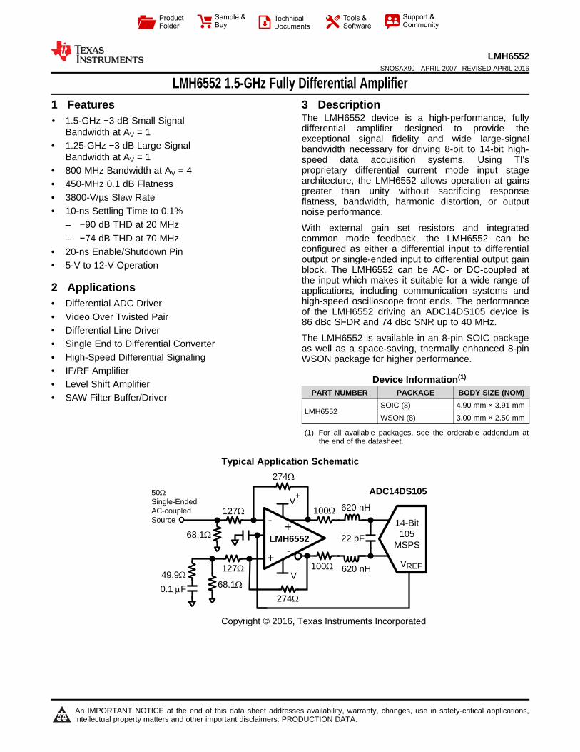
6 Specifications
6.1 Absolute Maximum Ratings (1) (2)
MIN MAX UNITSupply Voltage 13.2 VCommon Mode Input Voltage ±VS VMaximum Input Current (pins 1, 2, 7, 8) 30 mAMaximum Output Current (pins 4, 5) (3) mAMaximum Junction Temperature 150 °CStorage temperature, Tstg −65 150 °C
(1) JEDEC document JEP155 states that 500-V HBM allows safe manufacturing with a standard ESD control process.(2) JEDEC document JEP157 states that 250-V CDM allows safe manufacturing with a standard ESD control process.
6.2 ESD RatingsVALUE UNIT
V(ESD) Electrostatic discharge
Human-body model (HBM), per ANSI/ESDA/JEDEC JS-001 (1) ±2000
VCharged-device model (CDM), per JEDEC specification JESD22-C101 (2) ±750
Machine model (MM) ±250
(1) The maximum power dissipation is a function of TJ(MAX), θJA. The maximum allowable power dissipation at any ambient temperature isPD = (TJ(MAX)– TA) / θJA. All numbers apply for packages soldered directly onto a PC Board.
6.3 Recommended Operating ConditionsMIN NOM MAX UNIT
Operating Temperature Range (1) −40 +85 °CTotal Supply Voltage 4.5 12 V
(1) For more information about traditional and new thermal metrics, see the IC Package Thermal Metrics application report, SPRA953.
6.4 Thermal Information
THERMAL METRIC (1)LMH6552
UNITD NGS8 PINS 8 PINS
RθJA Junction-to-ambient thermal resistance 150 58 °C/W
5
LMH6552www.ti.com SNOSAX9J –APRIL 2007–REVISED APRIL 2016
Product Folder Links: LMH6552
Submit Documentation FeedbackCopyright © 2007–2016, Texas Instruments Incorporated
(1) Electrical Table values apply only for factory testing conditions at the temperature indicated. Factory testing conditions result in verylimited self-heating of the device such that TJ = TA. No specification of parametric performance is indicated in the electrical tables underconditions of internal self-heating where TJ > TA. See Overview for information on temperature de-rating of this device. Min/Max ratingsare based on product characterization and simulation. Individual parameters are tested as noted.
(2) Limits are 100% production tested at 25°C. Limits over the operating temperature range are ensured through correlation using StatisticalQuality Control (SQC) methods.
(3) Typical values represent the most likely parametric norm as determined at the time of characterization. Actual typical values can varyover time and also depend on the application and configuration. The typical values are not tested and are not ensured on shippedproduction material.
(4) IBoffset is referred to a differential output offset voltage by the following relationship: VOD(offset) = IBI*2RF.
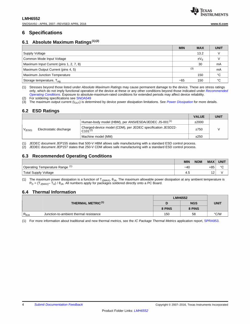
6.5 Electrical Characteristics: ±5 VUnless otherwise specified, all limits are ensured for TA = 25°C, V+ = +5 V, V− = −5 V, AV= 1, VCM = 0 V, RF = RG = 357 Ω, RL= 500 Ω, for single ended in, differential out. (1)
PARAMETER TEST CONDITIONS MIN (2) TYP (3) MAX (2) UNITAC PERFORMANCE (DIFFERENTIAL)SSBW Small Signal −3-dB Bandwidth (2) VOUT = 0.2 VPP, AV = 1, RL = 1 kΩ 1500
MHzVOUT = 0.2 VPP, AV = 1 1000VOUT = 0.2 VPP, AV = 2 930VOUT = 0.2 VPP, AV = 4 810VOUT = 0.2 VPP, AV = 8 590
LSBW Large Signal −3 dB Bandwidth VOUT = 2 VPP, AV = 1, RL = 1 kΩ 1250
MHzVOUT = 2 VPP, AV = 1 950VOUT = 2 VPP, AV = 2 820VOUT = 2 VPP, AV = 4 740VOUT = 2 VPP, AV = 8 590
0.1-dB Bandwidth VOUT = 0.2 VPP, AV = 1 450 MHzSlew Rate 4-V Step, AV = 1 3800 V/μsRise, Fall Time, 10%-90% 2-V Step 600 ps0.1% Settling Time 2-V Step 10 nsOverdrive Recovery Time VIN = 1.8-V to 0-V Step, AV = 5 V/V 6 ns
DISTORTION AND NOISE RESPONSEHD2 2nd Harmonic Distortion VOUT = 2 VPP, f = 20 MHz, RL = 800 Ω –92
dBcVOUT = 2 VPP, f = 70 MHz, RL = 800 Ω –74
HD3 3rd Harmonic Distortion VOUT = 2 VPP, f = 20 MHz, RL = 800 Ω –93dBc
VOUT = 2 VPP, f = 70 MHz, RL = 800 Ω –84IMD3 Two-Tone Intermodulation f ≥ 70 MHz, Third-Order Products, VOUT =
2-VPP Composite–87 dBc
Input Noise Voltage f ≥ 1 MHz 1.1 nV/√HzInput Noise Current f ≥ 1 MHz 19.5 pA/√HzNoise Figure (See Figure 46) 50-Ω System, AV = 9, 10 MHz 10.3 dB
INPUT CHARACTERISTICSIBI Input Bias Current (4) 60 110 µAIBoffset Input Bias Current Differential
(3)VCM = 0 V, VID = 0 V, IBoffset = (IB− - IB+)/2 2.5 18 µA
CMRR Common Mode Rejection Ratio (3) DC, VCM = 0 V, VID = 0 V 80 dBcRIN Input Resistance Differential 15 ΩCIN Input Capacitance Differential 0.5 pFCMVR Input Common Mode Voltage Range CMRR > 38 dB ±3.5 ±3.8 V

6
LMH6552SNOSAX9J –APRIL 2007–REVISED APRIL 2016 www.ti.com
Product Folder Links: LMH6552
Submit Documentation Feedback Copyright © 2007–2016, Texas Instruments Incorporated
Electrical Characteristics: ±5 V (continued)Unless otherwise specified, all limits are ensured for TA = 25°C, V+ = +5 V, V− = −5 V, AV= 1, VCM = 0 V, RF = RG = 357 Ω, RL= 500 Ω, for single ended in, differential out.(1)
PARAMETER TEST CONDITIONS MIN (2) TYP (3) MAX (2) UNIT
(5) Limit short circuit current in duration to no more than 10 seconds. See Power Dissipation for more details.(6) Negative input current implies current flowing out of the device.
OUTPUT PERFORMANCEOutput Voltage Swing (3) Differential Output 14.8 15.4 VPP
IOUT Linear Output Current (3) VOUT = 0 V ±70 ±80 mAISC Short Circuit Current One Output Shorted to Ground VIN = 2 V
Single Ended (5)±141 mA
Output Balance Error ΔVOUT Common Mode / ΔVOUTDifferential, ΔVOD = 1 V, f < 1 MHz
–60 dB
MISCELLANEOUS PERFORMANCEZT Open Loop Transimpedance Differential 108 dBΩPSRR Power Supply Rejection Ratio DC, (V+ - |V-|) = ±1 V 80 dBIS Supply Current (3) RL = ∞ 19 22.5 25
28 mA
Enable Voltage Threshold 3 VDisable Voltage Threshold 2.0 VEnable/Disable time 15 ns
ISD Disable Shutdown Current 500 600 μAOUTPUT COMMON MODE CONTROL CIRCUIT
Common Mode Small SignalBandwidth
VIN+ = VIN
− = 0 400 MHz
Slew Rate VIN+ = VIN
− = 0 607 V/μsVOSCM Input Offset Voltage Common Mode, VID = 0, VCM = 0 1.5 ±16.5 mV
Input Bias Current (6) –3.2 ±8 µAVoltage Range ±3.7 ±3.8 VCMRR Measure VOD, VID = 0 V 80 dBInput Resistance 200 kΩGain ΔVO,CM / ΔVCM 0.995 1.0 1.012 V/V

7
LMH6552www.ti.com SNOSAX9J –APRIL 2007–REVISED APRIL 2016
Product Folder Links: LMH6552
Submit Documentation FeedbackCopyright © 2007–2016, Texas Instruments Incorporated
(1) Electrical Table values apply only for factory testing conditions at the temperature indicated. Factory testing conditions result in verylimited self-heating of the device such that TJ = TA. No specification of parametric performance is indicated in the electrical tables underconditions of internal self-heating where TJ > TA. See Overview for information on temperature de-rating of this device." Min/Max ratingsare based on product characterization and simulation. Individual parameters are tested as noted.
(2) Limits are 100% production tested at 25°C. Limits over the operating temperature range are ensured through correlation using StatisticalQuality Control (SQC) methods.
(3) Typical values represent the most likely parametric norm as determined at the time of characterization. Actual typical values can varyover time and also depend on the application and configuration. The typical values are not tested and are not ensured on shippedproduction material.
(4) IBoffset is referred to a differential output offset voltage by the following relationship: VOD(offset) = IBI*2RF.(5) Limit short circuit current in duration to no more than 10 seconds. See Power Dissipation for more details.
6.6 Electrical Characteristics: ±2.5 VUnless otherwise specified, all limits are ensured for TA = 25°C, V+ = +2.5 V, V− = −2.5 V, AV = 1, VCM = 0 V, RF = RG =357 Ω, RL = 500 Ω, for single ended in, differential out. (1)
PARAMETER TEST CONDITIONS MIN (2) TYP (3) MAX (2) UNITSSBW Small Signal −3-dB Bandwidth (2) VOUT = 0.2 VPP, AV = 1, RL = 1 kΩ 1100
MHzVOUT = 0.2 VPP, AV = 1 800VOUT = 0.2 VPP, AV = 2 740VOUT = 0.2 VPP, AV = 4 660VOUT = 0.2 VPP, AV = 8 498
LSBW Large Signal −3 dB Bandwidth VOUT = 2 VPP, AV = 1, RL = 1 kΩ 820
MHzVOUT = 2 VPP, AV = 1 690VOUT = 2 VPP, AV = 2 620VOUT = 2 VPP, AV = 4 589VOUT = 2 VPP, AV = 8 480
0.1 dB Bandwidth VOUT = 0.2 VPP, AV = 1 300 MHzSlew Rate 2-V Step, AV = 1 2100 V/μsRise/Fall Time, 10% to 90% 2-V Step 700 ps0.1% Settling Time 2-V Step 10 nsOverdrive Recovery Time VIN = 0.7-V to 0-V Step, AV = 5 V/V 6 ns
DISTORTION AND NOISE RESPONSEHD2 2nd Harmonic Distortion VOUT = 2 VPP, f = 20 MHz, RL = 800 Ω -82
dBcVOUT = 2 VPP, f = 70 MHz, RL = 800 Ω -65
HD3 3rd Harmonic Distortion VOUT = 2 VPP, f = 20 MHz, RL = 800 Ω -79dBc
VOUT = 2 VPP, f = 70 MHz, RL = 800 Ω -67IMD3 Two-Tone Intermodulation f ≥ 70 MHz, Third-Order Products,
VOUT = 2-VPP Composite−77 dBc
Input Noise Voltage f ≥ 1 MHz 1.1 nV/√HzInput Noise Current f ≥ 1 MHz 19.5 pA/√HzNoise Figure (See Figure 46) 50-Ω System, AV = 9, 10 MHz 10.2 dB
INPUT CHARACTERISTICSIBI Input Bias Current (4) 54 90 µAIBoffset Input Bias Current Differential
(3)VCM = 0 V, VID = 0 V, IBoffset = (IB− - IB+ )/2 2.3 18 μA
CMRR Common-Mode Rejection Ratio (3) DC, VCM = 0 V, VID = 0 V 75 dBcRIN Input Resistance Differential 15 ΩCIN Input Capacitance Differential 0.5 pFCMVR Input Common Mode Range CMRR > 38 dB ±1.0 ±1.3 VOUTPUT PERFORMANCE
Output Voltage Swing (3) Differential Output 5.6 6.0 VPP
IOUT Linear Output Current (3) VOUT = 0 V ±55 ±65 mAISC Short Circuit Current One Output Shorted to Ground, VIN = 2 V
Single Ended (5)±131 mA

8
LMH6552SNOSAX9J –APRIL 2007–REVISED APRIL 2016 www.ti.com
Product Folder Links: LMH6552
Submit Documentation Feedback Copyright © 2007–2016, Texas Instruments Incorporated
Electrical Characteristics: ±2.5 V (continued)Unless otherwise specified, all limits are ensured for TA = 25°C, V+ = +2.5 V, V− = −2.5 V, AV = 1, VCM = 0 V, RF = RG =357 Ω, RL = 500 Ω, for single ended in, differential out.(1)
PARAMETER TEST CONDITIONS MIN (2) TYP (3) MAX (2) UNIT
(6) Negative input current implies current flowing out of the device.
Output Balance Error ΔVOUT Common Mode / ΔVOUTDifferential, ΔVOD = 1 V, f < 1 MHz
60 dB
MISCELLANEOUS PERFORMANCEZT Open Loop Transimpedance Differential 107 dBΩPSRR Power Supply Rejection Ratio DC, ΔVS = ±1 V 80 dBIS Supply Current (3) RL = ∞ 17 20.4 24
27 mA
Enable Voltage Threshold 0.5 VDisable Voltage Threshold –0.5 VEnable/Disable Time 15 ns
ISD Disable Shutdown Current 500 600 µAOUTPUT COMMON MODE CONTROL CIRCUIT
Common Mode Small SignalBandwidth
VIN+ = VIN
− = 0 310 MHz
Slew Rate VIN+ = VIN
− = 0 430 V/μsVOSCM Input Offset Voltage Common Mode, VID = 0, VCM = 0 1.65 ±15 mV
Input Bias Current (6) −2.9 µAVoltage Range ±1.19 ±1.25 VCMRR Measure VOD, VID = 0 V 80 dBInput Resistance 200 kΩGain ΔVO,CM / ΔVCM 0.995 1.0 1.012 V/V

-9
-8
-7
-6
-5
-4
-3
-2
-1
0
1
2
3
1 10 100 10000
FREQUENCY (MHz)
NO
RM
ALI
ZE
D G
AIN
(dB
)
1000
V+ = +2.5V
V- = -2.5V
RL = 500:
RF = 357:
VOD = 0.2 VPP
AV = 1 V/V
V+ = +5V
V- = -5V
RL = 500:
RF = 357:
DIFFERENTIAL INPUT-9
-8
-7
-6
-5
-4
-3
-2
-1
0
1
2
3
1 10 100 10000
FREQUENCY (MHz)
NO
RM
ALI
ZE
D G
AIN
(dB
)
1000
V+ = +2.5V
V- = -2.5V
RL = 1 k:
RF = 301:
VOD = 0.2 VPP
AV = 1 V/V
V+ = +5V
V- = -5V
RL = 1 k:
RF = 301:
DIFFERENTIAL INPUT
1 10 100 1000 10000
FREQUENCY (MHz)
-9
-8
-7
-6
-5
-4
-3
-2
-1
0
1
NO
RM
ALI
ZE
D G
AIN
(dB
)
V+ = +5V
V- = -5V
AV = 2 V/VDIFFERENTIAL INPUT
VOD = 4 VPP
VOD = 2 VPP
VOD = 0.5 VPP
1 10 100 1000 10000
FREQUENCY (MHz)
-9
-8
-7
-6
-5
-4
-3
-2
-1
0
1
NO
RM
ALI
ZE
D G
AIN
(dB
)
V+ = +5V
V- = -5V
AV = 2 V/VSINGLE-ENDED INPUT
VOD = 4 VPP
VOD = 2 VPP
VOD = 0.5 VPP
1 10 100 1000 10000
FREQUENCY (MHz)
-9
-8
-7
-6
-5
-4
-3
-2
-1
0
1
NO
RM
ALI
ZE
D G
AIN
(dB
)
AV = 8, RF = 400:
VOUT = 0.2 VPP
SINGLE-ENDED INPUT
AV = 4
AV = 2
AV = 1
1 10 100 1000 10000FREQUENCY (MHz)
-9
-8
-7
-6
-5
-4
-3
-2
-1
0
1
NO
RM
ALI
ZE
D G
AIN
(dB
)
VOUT = 0.2 VPP
DIFFERENTIAL INPUT
AV = 8
AV = 4
AV = 1
AV = 2
9
LMH6552www.ti.com SNOSAX9J –APRIL 2007–REVISED APRIL 2016
Product Folder Links: LMH6552
Submit Documentation FeedbackCopyright © 2007–2016, Texas Instruments Incorporated
6.7 Typical Characteristics V+ = +5 V, V− = −5 V(TA = 25°C, RF = RG = 357 Ω, RL = 500 Ω, AV = 1, for single ended in, differential out, unless specified).
Figure 1. Frequency Response vs Gain Figure 2. Frequency Response vs Gain
Figure 3. Frequency Response vs VOUT Figure 4. Frequency Response vs VOUT
Figure 5. Frequency Response vs Supply Voltage Figure 6. Frequency Response vs Supply Voltage

0 5 10 15 20 25 30 35 40 45 50-1.5
-1
-0.5
0
0.5
1
1.5
VO
D (
V)
TIME (ns)
V+
= +5
V- = -5V
RL = 500:
RF = 357:
0 5 10 15 20 25 30 35 40 45 50-2.5
-2
-1.5
-1
-0.5
0
0.5
1
1.5
2
2.5
VO
D (
V)
TIME (ns)
V+ = +5V
V- = -5V
RL = 500:
RF = 357:
0 5 10 15 20 25 30 35 40 45 50-0.8
-0.6
-0.4
-0.2
0
0.2
0.4
0.6
0.8
VO
D (
V)
TIME (ns)
V+ = +2.5V
V- = -2.5V
RL = 500:
RF = 357:
1 10000
FREQUENCY (MHz)
-9
-5
-2
2
NO
RM
ALI
ZE
D G
AIN
(dB
)
100010010
0
-4
-8
1
-1
-3
-6
-7
V+ = +5V
V- = -5V
AV = 1 V/V
VOUT = 2 VPP
RL = 1 k:
RF = 301:
RF = 357:
RF = 400:
DIFFERENTIAL INPUT
1 10 100 1000 10000
FREQUENCY (MHz)
-9
-8
-7
-6
-5
-4
-3
-2
-1
0
1N
OR
MA
LIZ
ED
GA
IN (
dB)
RL = 200:
RL = 1 k:
RL = 500:
RL = 800:
V+ = +5V
V- = -5V
AV = 1 V/V
RF = 357:
VOUT = 0.2 VPP
SINGLE-ENDED INPUT
1 10 100 1000 10000
FREQUENCY (MHz)
-9
-8
-7
-6
-5
-4
-3
-2
-1
0
1
NO
RM
ALI
ZE
D G
AIN
(dB
)
RL = 200:
RL = 1 k:
RL = 500:
RL = 800:
V+ = +5V
V- = -5V
AV = 1 V/V
RF = 357:
VOUT = 2 VPP
SINGLE-ENDED INPUT
10
LMH6552SNOSAX9J –APRIL 2007–REVISED APRIL 2016 www.ti.com
Product Folder Links: LMH6552
Submit Documentation Feedback Copyright © 2007–2016, Texas Instruments Incorporated
Typical Characteristics V+ = +5 V, V− = −5 V (continued)(TA = 25°C, RF = RG = 357 Ω, RL = 500 Ω, AV = 1, for single ended in, differential out, unless specified).
Figure 7. Frequency Response vs Resistive Load Figure 8. Frequency Response vs Resistive Load
Figure 9. Frequency Response vs RF Figure 10. 1 VPP Pulse Response Single Ended Input
Figure 11. 2 VPP Pulse Response Single Ended Input Figure 12. Large Signal Pulse Response
0 0.5 1 1.5 2 2.5 3
VOCM (V)
-100
-90
-80
-70
-60
-50
-40
DIS
TO
RT
ION
(dB
c)
V+ = +5V
V- = -5V
RL = 800:
VOUT = 2 VPP
fc = 20 MHz
HD2
HD3
0 0.5 1 1.5 2 2.5 3
VOCM (V)
-90
-80
-70
-60
-50
-40
DIS
TO
RT
ION
(dB
c)
HD2
HD3
V+ = +5V
V- = -5V
RL = 800:
VOUT = 2 VPP
fc = 75 MHz
HD2
HD3
3 5 7 9 11 12-90
-80
-70
-60
-50
-20
DIS
TO
RT
ION
(dB
c)
TOTAL SUPPLY VOLTAGE (V)
-40
-30
RL = 800:
VOUT = 2 VPP
fc = 75 MHz
FREQUENCY (MHz)
DIS
TO
RT
ION
(dB
c)
-50
-55
-60
-65
-70
-75
-80
-85
-90
-95
-100
-1051 25 50 75 100 125 150 175 200 225 250
HD2
HD3
V+ = +5VV- = -5VRL = 800ÖVOD = 2 VPP
VOCM = 0V
0 5 10 15 20 25 30 35 40 45 50-80
-60
-40
-20
0
20
40
60
80C
OM
MO
N M
OD
E V
OU
T (
mV
)
TIME (ns)
V+ = +5V
V- = -5V
RL = 500:
RL = 357:
VOD = 2 VPP
11
LMH6552www.ti.com SNOSAX9J –APRIL 2007–REVISED APRIL 2016
Product Folder Links: LMH6552
Submit Documentation FeedbackCopyright © 2007–2016, Texas Instruments Incorporated
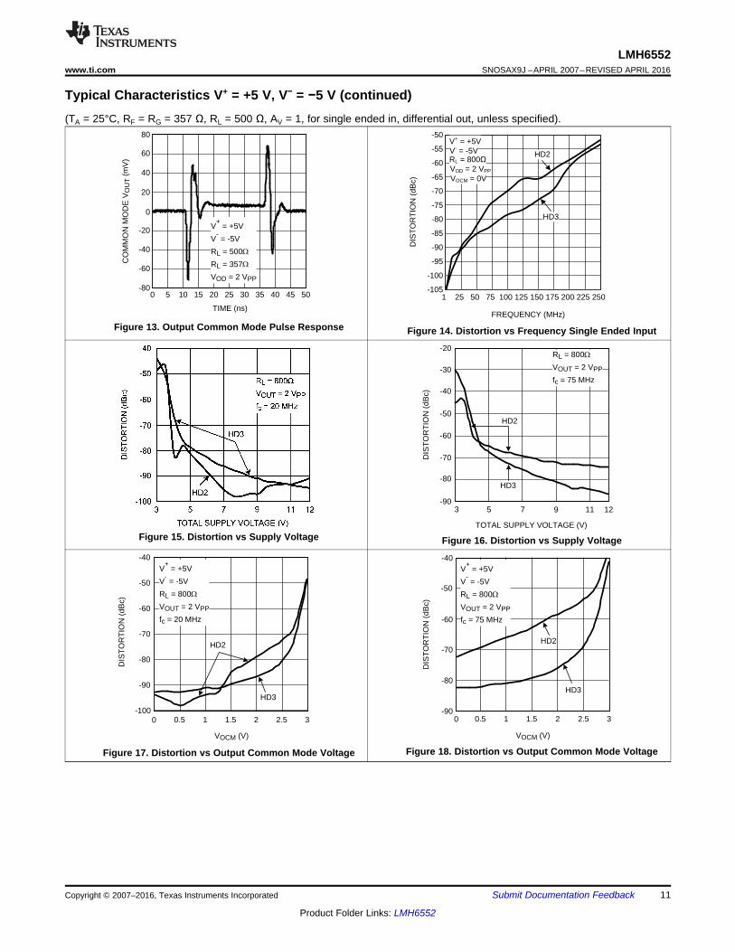
Typical Characteristics V+ = +5 V, V− = −5 V (continued)(TA = 25°C, RF = RG = 357 Ω, RL = 500 Ω, AV = 1, for single ended in, differential out, unless specified).
Figure 13. Output Common Mode Pulse Response Figure 14. Distortion vs Frequency Single Ended Input
Figure 15. Distortion vs Supply Voltage Figure 16. Distortion vs Supply Voltage
Figure 17. Distortion vs Output Common Mode Voltage Figure 18. Distortion vs Output Common Mode Voltage

0.01 1 100 1000
FREQUENCY (MHz)
0.0001
10
1000
|Z| (:
)
100.1
100
0.001
0.1
1
0.01
V+ = +5V
V- = -5V
VIN = 0V
AV = 1 V/V
0.01 0.1 1 10 1000
FREQUENCY (MHz)
0.01
0.1
100
1000
|Z| (:
)
100
1
10
V+ = +2.5V
V- = -2.5
VIN = 0V
AV = 1 V/V
120
0.01 1 1000
FREQUENCY (MHz)
40
70
MA
GN
ITU
DE
, |Z
| (dB
:)
100100.1
100
90
60
50
80
110
-180
-45
-90
-135
0
MAGNITUDE
PHASE
V+ = +5V
V- = -5V
PH
AS
E (
°)
120
0.01 1 1000
FREQUENCY (MHz)
40
70
MA
GN
ITU
DE
, |Z
| (dB
:)
100100.1
100
90
60
50
80
110
-180
-45
-90
-135
0
MAGNITUDE
PHASE
V+ = +2.5V
V- = -2.5V
PH
AS
E (
°)
4
0 -10 -20 -30 -40 -50 -602
2.2
2.4
2.6
2.8
3
3.2
3.4
3.6
3.8
MA
XIM
UM
VO
UT (
V)
OUTPUT CURRENT (mA)
V+ = +5V
V- = -5V
RF = 357:
VIN = 3.8V SINGLE-ENDED INPUT
-2
0 10 20 30 40 50 60-4
-3.8
-3.6
-3.4
-3.2
3
-2.8
-2.6
-2.4
-2.2
OUTPUT CURRENT (mA)
V+ = +5V
V- = -5V
RF = 357:
VIN = 3.8V SINGLE-ENDED
MIN
IMU
M V
OU
T (
V)
12
LMH6552SNOSAX9J –APRIL 2007–REVISED APRIL 2016 www.ti.com
Product Folder Links: LMH6552
Submit Documentation Feedback Copyright © 2007–2016, Texas Instruments Incorporated
Typical Characteristics V+ = +5 V, V− = −5 V (continued)(TA = 25°C, RF = RG = 357 Ω, RL = 500 Ω, AV = 1, for single ended in, differential out, unless specified).
Figure 19. Maximum VOUT vs IOUT Figure 20. Minimum VOUT vs IOUT
Figure 21. Open Loop Transimpedance Figure 22. Open Loop Transimpedance
Figure 23. Closed Loop Output Impedance Figure 24. Closed Loop Output Impedance

0.1 1 1000
FREQUENCY (MHz)
20
40
65
85
CM
RR
(dB
)
10010
75
55
30
25
35
45
50
60
70
80
AV = 2 V/V
RL = 500:
RF = 357:
VOUT = 1.0 VPP
1 1000
FREQUENCY (MHz)
-70
-50
-30
-10
BA
LAN
CE
ER
RO
R (
dBc)
10010
-20
-40
-60
-15
-25
-35
-45
-55
-65
V+ = +2.5V
V- = -2.5V
RL = 500:
RF = 357:
AV = 1 V/V
V+ = +5V
V- = -5V
0
40
100
PS
RR
(dB
c D
IFF
ER
EN
TIA
L) 80
60
20
90
70
50
30
10
1 1000
FREQUENCY (MHz)
100100.1
+PSRR
-PSRR
V+ = +5V
V- = -5V
AV = 2 V/V
RL = 500:
VIN = 0V
0.1 1000
FREQUENCY (MHz)
0
-40
-70
-110
PS
RR
(dB
c D
IFF
ER
EN
TIA
L)
100101
-90
-50
-10
-100
-80
-60
-30
-20
+PSRR
-PSRR
V+ = +2.5V
V- = -2.5V
AV = 2 V/V
RL = 500:
VIN = 0V
0 200 400 600 800 1000-10
-8
-6
-4
-2
0
2
4
6
8
10
OU
TP
UT
VO
LTA
GE
(V
OD
)
TIME (ns)
V+ = +5V
V- = -5V
AV = 5 V/V
RF = 324:
RL = 200:-2
-1.6
-1.2
-0.8
-0.4
0
0.4
0.8
1.2
1.6
2
INP
UT
VO
LTA
GE
(V
)
INPUT
OUTPUT
0 200 400 600 800 1000-4
-3
-2
-1
0
1
2
3
4
OU
TP
UT
VO
LTA
GE
(V
OD
)
TIME (ns)
-0.8
-0.6
-0.4
-0.2
0
0.2
0.4
0.6
0.8
INP
UT
VO
LTA
GE
(V
)
V+ = +2.5V
V- = -2.5V
AV = 5 V/V
RF = 324:
RL = 200:
INPUT
OUTPUT
13
LMH6552www.ti.com SNOSAX9J –APRIL 2007–REVISED APRIL 2016
Product Folder Links: LMH6552
Submit Documentation FeedbackCopyright © 2007–2016, Texas Instruments Incorporated
Typical Characteristics V+ = +5 V, V− = −5 V (continued)(TA = 25°C, RF = RG = 357 Ω, RL = 500 Ω, AV = 1, for single ended in, differential out, unless specified).
Figure 25. Overdrive Recovery Figure 26. Overdrive Recovery
Figure 27. PSRR Figure 28. PSRR
Figure 29. CMRR Figure 30. Balance Error

10 100 1000-300
-200
-100
0
100
200
300
400
PH
AS
E (
°)
FREQUENCY (MHz)
S11
S22
S12
S11(SINGLE-ENDED INPUT) S21
V+ = +5V
V- = -5V
AV = 1 V/V
0 1 2 3 4 5 6 7-110
-100
-90
-80
-70
-60
-50
-40
-30
-20
IMD
3 (
dBc)
DIFFERENTIAL VOUT (VPP)
fc = 75 MHz (200 kHz SPACING)SINGLE-ENDED INPUT
RL = 200:
RL = 800:
V+ = +5V
V- = -5V
RF = 357:
AV = 2 V/V
0.0001 0.01 1 100
FREQUENCY (MHz)
100.10.001
VO
LTA
GE
NO
ISE
(nV
/H
z) NOISE VOLTAGE
INVERTING CURRENT NOISE CURRENT
NON-INVERTING CURRENT NOISE CURRENT
6
0
4
5
3
2
1
210
0
140
175
105
70
35 CU
RR
EN
T N
OIS
E (
pA/
Hz)
10 100 1000-80
-70
-60
-50
-40
-30
-20
-10
0
MA
GN
ITU
DE
(dB
)
FREQUENCY (MHz)
V+ = +5V
V- = -5V
AV = 1 V/V
S21S22
S11
S12
S11 (SINGLE-ENDED
INPUT)
0 20 40 60 80 100 120 140 160 180 20010
11
12
13
14
15N
OIS
E F
IGU
RE
(dB
)
FREQUENCY (MHz)
V+ = +5V
V- = -5V
AV = 9 V/V
RF = 275:50: SYSTEM
0 20 40 60 80 100 120 140 160 180 20010
11
12
13
14
15
NO
ISE
FIG
UR
E (
dB)
FREQUENCY (MHz)
V+ = +2.5V
V- = -2.5V
AV = 9 V/V
RF = 275:50: SYSTEM
14
LMH6552SNOSAX9J –APRIL 2007–REVISED APRIL 2016 www.ti.com
Product Folder Links: LMH6552
Submit Documentation Feedback Copyright © 2007–2016, Texas Instruments Incorporated
Typical Characteristics V+ = +5 V, V− = −5 V (continued)(TA = 25°C, RF = RG = 357 Ω, RL = 500 Ω, AV = 1, for single ended in, differential out, unless specified).
Figure 31. Noise Figure Figure 32. Noise Figure
Figure 33. Input Noise vs Frequency Figure 34. Differential S-Parameter Magnitude vs Frequency
Figure 35. Differential S-Parameter Phase vs Frequency Figure 36. 3rd Order Intermodulation Products vs VOUT

0 1 2 3 4 5 6 7-110
-100
-90
-80
-70
-60
-50
-40
-30
-20
IMD
3 (
dBc)
DIFFERENTIAL VOUT (VPP)
fc = 75 MHz (200 kHz SPACING)
SINGLE-ENDED INPUT
RL = 200:
RL = 800:
V+ = +2.5V
V- = -2.5V
RF = 357:
AV = 2 V/V
50 60 70 80 90 100-100
-95
-90
-85
-80
-75
-70
-65
IMD
3 (
dBc)
CENTER FREQUENCY (MHz)
V+ = +2.5V
V- = -2.5V
V+ = +5V
V- = -5V
RL = 800:
RF = 360:
AV = +2
VOD = 2 VPP
SINGLE-ENDED INPUT200 kHz SPACING
15
LMH6552www.ti.com SNOSAX9J –APRIL 2007–REVISED APRIL 2016
Product Folder Links: LMH6552
Submit Documentation FeedbackCopyright © 2007–2016, Texas Instruments Incorporated
Typical Characteristics V+ = +5 V, V− = −5 V (continued)(TA = 25°C, RF = RG = 357 Ω, RL = 500 Ω, AV = 1, for single ended in, differential out, unless specified).
Figure 37. 3rd Order Intermodulation Products vs VOUT Figure 38. 3rd Order Intermodulation Productsvs Center Frequency
V+
-IN
+
±
High-AolDifferential I/OAmplifier
+IN
2.5 k
2.5 k
+OUT
-OUT
+
±
+
±
VcmError
AmplifierVCM
V+
VEN Buffer
V±
High Impedance
Copyright © 2016, Texas Instruments Incorporated
16
LMH6552SNOSAX9J –APRIL 2007–REVISED APRIL 2016 www.ti.com
Product Folder Links: LMH6552
Submit Documentation Feedback Copyright © 2007–2016, Texas Instruments Incorporated
7 Detailed Description
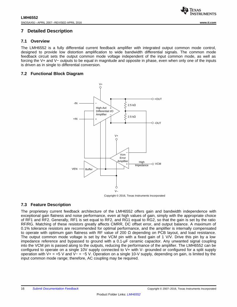
7.1 OverviewThe LMH6552 is a fully differential current feedback amplifier with integrated output common mode control,designed to provide low distortion amplification to wide bandwidth differential signals. The common modefeedback circuit sets the output common mode voltage independent of the input common mode, as well asforcing the V+ and V− outputs to be equal in magnitude and opposite in phase, even when only one of the inputsis driven as in single to differential conversion.
7.2 Functional Block Diagram
7.3 Feature DescriptionThe proprietary current feedback architecture of the LMH6552 offers gain and bandwidth independence withexceptional gain flatness and noise performance, even at high values of gain, simply with the appropriate choiceof RF1 and RF2. Generally, RF1 is set equal to RF2, and RG1 equal to RG2, so that the gain is set by the ratioRF/RG. Matching of these resistors greatly affects CMRR, DC offset error, and output balance. A maximum of0.1% tolerance resistors are recommended for optimal performance, and the amplifier is internally compensatedto operate with optimum gain flatness with RF value of 200 Ω depending on PCB layout, and load resistance.The output common mode voltage is set by the VCM pin with a fixed gain of 1 V/V. Drive this pin by a lowimpedance reference and bypassed to ground with a 0.1-μF ceramic capacitor. Any unwanted signal couplinginto the VCM pin is passed along to the outputs, reducing the performance of the amplifier. The LMH6552 can beconfigured to operate on a single 10V supply connected to V+ with V- grounded or configured for a split supplyoperation with V+ = +5 V and V− = −5 V. Operation on a single 10-V supply, depending on gain, is limited by theinput common mode range; therefore, AC coupling may be required.
17
LMH6552www.ti.com SNOSAX9J –APRIL 2007–REVISED APRIL 2016
Product Folder Links: LMH6552
Submit Documentation FeedbackCopyright © 2007–2016, Texas Instruments Incorporated
7.4 Device Functional ModesThis wideband FDA requires external resistors for correct signal-path operation. When configured for the desiredinput impedance and gain setting with these external resistors, the amplifier can be either on with the PD pinasserted to a voltage greater than Vs– + 3.0 V, or turned off by asserting PD low. Disabling the amplifier shutsoff the quiescent current and stops correct amplifier operation. The signal path is still present for the sourcesignal through the external resistors. The Vocm control pin sets the output average voltage. Left open, Vocmfloats to an indeterminate voltage. Driving this high-impedance input with a voltage reference within its validrange sets a target for the internal Vcm error amplifier.
8 Application and Implementation
NOTEInformation in the following applications sections is not part of the TI componentspecification, and TI does not warrant its accuracy or completeness. TI’s customers areresponsible for determining suitability of components for their purposes. Customers shouldvalidate and test their design implementation to confirm system functionality.
8.1 Application InformationThe proprietary current feedback architecture of the LMH6552 offers gain and bandwidth independence withexceptional gain flatness and noise performance, even at high values of gain, simply with the appropriate choiceof RF1 and RF2. Generally RF1 is set equal to RF2, and RG1 equal to RG2, so that the gain is set by the ratio RF/RG.Matching of these resistors greatly affects CMRR, DC offset error, and output balance. A minimum of 0.1%tolerance resistors are recommended for optimal performance, and the amplifier is internally compensated tooperate with optimum gain flatness with values of RF between 270 Ω and 390 Ω depending on packageselection, PCB layout, and load resistance.
The output common mode voltage is set by the VCM pin with a fixed gain of 1 V/V. This pin must be driven by alow impedance reference and must be bypassed to ground with a 0.1 µF ceramic capacitor. Any unwanted signalcoupling into the VCM pin is passed along to the outputs, reducing the performance of the amplifier. This pin mustnot be left floating.
The LMH6552 can be operated on a supply range as either a single 5V supply or as a split +5 V and −5 V.Operation on a single 5-V supply, depending on gain, is limited by the input common mode range; therefore, ACcoupling may be required. For example, in a DC coupled input application on a single 5-V supply, with a VCM of1.5 V, the input common voltage at a gain of 1 is 0.75 V, which is outside the minimum 1.2-V to 3.8-V inputcommon mode range of the amplifier. The minimum VCM for this application must be greater than 2.5 Vdepending on output signal swing. Alternatively, AC coupling of the inputs in this example results in equal inputand output common mode voltages, so a 1.5 V VCM would be achievable. Split supplies allow much lessrestricted AC and DC coupled operation with optimum distortion performance.
The LMH6552 is equipped with an ENABLE pin to reduce power consumption when not in use. The ENABLEpin, when not driven, floats high (on). When the ENABLE pin is pulled low the amplifier is disabled and theamplifier output stage goes into a high impedance state so the feedback and gain set resistors determine theoutput impedance of the circuit. For this reason input to output isolation is poor in the disabled state and the partis not recommended in multiplexed applications where outputs are all tied together.
8.2 Typical Applications
8.2.1 Typical Fully Differential ApplicationIn many applications, it is required to drive a differential input ADC from a single ended source. Traditionally,transformers have been used to provide single to differential conversion, but these are inherently bandpass bynature and cannot be used for DC coupled applications. The LMH6552 provides excellent performance as asingle-to-differential converter down to DC. Figure 45 illustrates a typical application circuit where an LMH6552 isused to produce a differential signal from a single ended source.

VS
RG
RG
VCMRL VO
RF
RF
CL
RO
RO
ENABLE
a
+
-
Copyright © 2016, Texas Instruments Incorporated
18
LMH6552SNOSAX9J –APRIL 2007–REVISED APRIL 2016 www.ti.com
Product Folder Links: LMH6552
Submit Documentation Feedback Copyright © 2007–2016, Texas Instruments Incorporated
Typical Applications (continued)
Figure 39. Typical Fully Differential Application Schematic
8.2.1.1 Design RequirementsOne typical application for the LMH6552 is to drive an ADC. The following design is a single ended to differentialcircuit with an input impedance of 50 Ω and an output impedance of 100 Ω. The VCM voltage of the amplifierneeds to be set to the same voltage as the ADC reference voltage which is typically 1.2 V. Figure 45 illustratesthe design equations required to set the external resistor values. This design also requires a gain of 1 and -74dBc THD at 70 MHz.
8.2.1.2 Detailed Design ProcedureTo match the input impedance of the circuit in Figure 45 to a specified source resistance, RS, requires that RT ||RIN = RS. The equations governing RIN and AV for single-to-differential operation are also provided inFigure 45. These equations, along with the source matching condition, must be solved iteratively to achieve thedesired gain with the proper input termination. Component values for several common gain configurations in a50-Ω environment are given in Table 1. Gain Component Values for 50-Ω System WSON Package. TypicallyRS=50 Ω and RM=RS||RT.
8.2.1.2.1 WSON Package
Due to its size and lower parasitics, the WSON requires the lower optimum value of 275 Ω for RF. This gives aflat frequency response with minimal peaking. With a lower RF value the WSON package has a reduction innoise compared to the SOIC with its optimum RF = 360 Ω.
8.2.1.2.2 Fully Differential Operation
The LMH6552 performs best in a fully differential configuration. The circuit illustrated in Figure 39 is a typical fullydifferential application circuit as might be used to drive an analog to digital converter (ADC). In this circuit theclosed loop gain AV = VOUT/ VIN = RF/RG, where the feedback is symmetric. The series output resistors, RO, areoptional and help keep the amplifier stable when presented with a capacitive load. Refer to Driving CapacitiveLoads for details.
When driven from a differential source, the LMH6552 provides low distortion, excellent balance, and commonmode rejection. This is true provided the resistors RF, RG and RO are well matched and strict symmetry isobserved in board layout. With an intrinsic device CMRR of 80 dB, using 0.1% resistors gives a worst caseCMRR of around 60 dB for most circuits.
The circuit configuration illustrated in Figure 40 was used to measure differential S parameters in a 50-Ωenvironment at a gain of 1 V/V. Refer to Figure 34 and Figure 35 in the Typical Characteristics for measurementresults.

VS VCMRL
357:
50:
ENABLE
a
+
-
357:
348:
348:
50:26.4:
56.2:
RS = 50:
VS VCM RL
357:
50:
ENABLE
a
+
-
357:
357:
357:
50:58:
58:RS = 50:
RS = 50:
19
LMH6552www.ti.com SNOSAX9J –APRIL 2007–REVISED APRIL 2016
Product Folder Links: LMH6552
Submit Documentation FeedbackCopyright © 2007–2016, Texas Instruments Incorporated
Typical Applications (continued)
Figure 40. Differential S-Parameter Test Circuit
Table 1. Gain Component Values for 50Ω System WSON PackageGain RF RG RT RM
0 dB 275Ω 255Ω 59Ω 26.7Ω6 dB 275Ω 127Ω 68.1Ω 28.7Ω12 dB 275Ω 54.9Ω 107Ω 34Ω
Figure 41. Single Ended Input S-Parameter Test Circuit (50Ω System)
The circuit shown in Figure 41 was used to measure S-parameters for a single-to-differential configuration.Figure 34 and Figure 35 in Typical Characteristics are taken using the recommended component values for 0 dBgain.
8.2.1.2.3 Driving Capacitive Loads
As noted previously, capacitive loads must be isolated from the amplifier output with small valued resistors. Thisis particularly the case when the load has a resistive component that is 500 Ω or higher. A typical ADC hascapacitive components of around 10 pF and the resistive component could be 1000 Ω or higher. If driving atransmission line, such as 50Ω coaxial or 100Ω twisted pair, using matching resistors is sufficient to isolate anysubsequent capacitance.
8.2.1.2.3.1 Balanced Cable Driver
With up to 15 VPP differential output voltage swing and 80 mA of linear drive current the LMH6552 makes anexcellent cable driver as illustrated in Figure 42. The LMH6552 is also suitable for driving differential cables froma single ended source.

1 10 100 1000
FREQUENCY (MHz)
-9
-8
-7
-6
-5
-4
-3
-2
-1
0
1
NO
RM
ALI
ZE
D G
AIN
(dB
)
CL = 82 pF, RO = 16:
CL = 39 pF, RO = 21:
CL = 15 pF, RO = 24:
CL = 5.6 pF, RO = 23:
VOD = 200 mVPP
AV = 1LOAD = (CL || 1 k:) IN
SERIES WITH 2 ROUTS
CAPACITIVE LOAD (pF)
1 10 1000
10
20
30
SU
GG
ES
TE
D R
O (:
)
V+ = +5V
V- = -5V
LOAD = 1 k: || CAP LOAD
VS
VCM
ENABLE
100: TWISTED PAIR50:
2 VPP
357:
169:
AV = 2 V/V
50:
a
+
-
357:
169:27.6:
61.8:
RS = 50:
20
LMH6552SNOSAX9J –APRIL 2007–REVISED APRIL 2016 www.ti.com
Product Folder Links: LMH6552
Submit Documentation Feedback Copyright © 2007–2016, Texas Instruments Incorporated
Figure 42. Fully Differential Cable Driver
8.2.1.3 Application CurvesMany application circuits have capacitive loading. As shown in Figure 43 amplifier bandwidth is reduced withincreasing capacitive load, so parasitic capacitance must be strictly limited.
In order to ensure stability resistance must be added between the capacitive load and the amplifier output pins.The value of the resistor is dependent on the amount of capacitive load as shown in Figure 44. This resistivevalue is a suggestion. System testing is required to determine the optimal value. Using a smaller resistor retainsmore system bandwidth at the expense of overshoot and ringing, and larger values of resistance reduceovershoot but also reduce system bandwidth.
Figure 43. Frequency Response vs Capacitive Load Figure 44. Suggested ROUT vs Capacitive Load
RG
RG
RF
RF
RO+
-RO
LMH6552
IN-
IN+
ADC
V+
V-
VO+
-RT
RS
RM
VS
AV, RIN
a
AV = 2(1 - E1)E1 + E2¨
¨
©
§ ¨¨
©
§
RIN =2RG + RM (1-E2)
1 + E2¨¨©
§ ¨¨©
§ E2 =
RG + RM
RG + RF + RM¨¨©
§ ¨¨©
§
¨¨
©
§E1 =
RGRG + RF
¨¨
©
§
RS = RT || RIN
RM= RT || RS
+-
VCM
Copyright © 2016, Texas Instruments Incorporated
21
LMH6552www.ti.com SNOSAX9J –APRIL 2007–REVISED APRIL 2016
Product Folder Links: LMH6552
Submit Documentation FeedbackCopyright © 2007–2016, Texas Instruments Incorporated
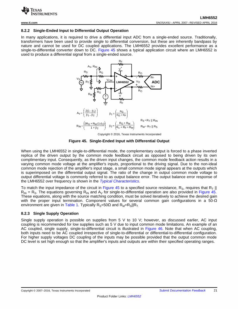
8.2.2 Single-Ended Input to Differential Output OperationIn many applications, it is required to drive a differential input ADC from a single-ended source. Traditionally,transformers have been used to provide single to differential conversion, but these are inherently bandpass bynature and cannot be used for DC coupled applications. The LMH6552 provides excellent performance as asingle-to-differential converter down to DC. Figure 45 shows a typical application circuit where an LMH6552 isused to produce a differential signal from a single-ended source.
Figure 45. Single-Ended Input with Differential Output
When using the LMH6552 in single-to-differential mode, the complementary output is forced to a phase invertedreplica of the driven output by the common mode feedback circuit as opposed to being driven by its owncomplimentary input. Consequently, as the driven input changes, the common mode feedback action results in avarying common mode voltage at the amplifier's inputs, proportional to the driving signal. Due to the non-idealcommon mode rejection of the amplifier's input stage, a small common mode signal appears at the outputs whichis superimposed on the differential output signal. The ratio of the change in output common mode voltage tooutput differential voltage is commonly referred to as output balance error. The output balance error response ofthe LMH6552 over frequency is shown in the Typical Characteristics.
To match the input impedance of the circuit in Figure 45 to a specified source resistance, RS, requires that RT ||RIN = RS. The equations governing RIN and AV for single-to-differential operation are also provided in Figure 45.These equations, along with the source matching condition, must be solved iteratively to achieve the desired gainwith the proper input termination. Component values for several common gain configurations in a 50-Ωenvironment are given in Table 1. Typically RS=50Ω and RM=RS||RT.
8.2.3 Single Supply OperationSingle supply operation is possible on supplies from 5 V to 10 V; however, as discussed earlier, AC inputcoupling is recommended for low supplies such as 5 V due to input common mode limitations. An example of anAC coupled, single supply, single-to-differential circuit is illustrated in Figure 46. Note that when AC coupling,both inputs need to be AC coupled irrespective of single-to-differential or differential-to-differential configuration.For higher supply voltages DC coupling of the inputs may be possible provided that the output common modeDC level is set high enough so that the amplifier's inputs and outputs are within their specified operating ranges.

169:
+
-
LMH6552
V+
V-
2.2 pF
VREF169:
-
+
125:
125:
357:
357:
ADC12DL080
12-Bit 80 MSPS
CIN
~ 7- 8 pF61.8:
50:Single-Ended AC-coupled Source
61.8:49.9:
0.1 PF
Copyright © 2016, Texas Instruments Incorporated
RG
RG
VCMRL VO
RF
RF
CL
RO
RO
ENABLE
+
-
VSa
VO1
VO2VI2
VI1
RM
RT
RS
VICM = VOCM
VICM = VI1 + VI2
2
*VCM =VO1 + VO2
2*BY DESIGN
Copyright © 2016, Texas Instruments Incorporated
22
LMH6552SNOSAX9J –APRIL 2007–REVISED APRIL 2016 www.ti.com
Product Folder Links: LMH6552
Submit Documentation Feedback Copyright © 2007–2016, Texas Instruments Incorporated
Figure 46. AC Coupled for Single Supply Operation
8.2.4 Split Supply OperationFor optimum performance, split supply operation is recommended using +5 V and −5 V supplies; however,operation is possible on split supplies as low as +2.25 V and −2.25 V and as high as +6 V and −6 V. Providedthe total supply voltage does not exceed the 4.5-V to 12-V operating specification, non-symmetric supplyoperation is also possible and in some cases advantageous. For example, if a 5-V DC coupled operation isrequired for low power dissipation but the amplifier input common mode range prevents this operation, it is stillpossible with split supplies of (V+) and (V−). Where (V+) - (V−) = 5V and V+ and V− are selected to center theamplifier input common mode range to suit the application.
Figure 47. Split Supply
8.2.5 Output Noise Performance and MeasurementUnlike differential amplifiers based on voltage feedback architectures, noise sources internal to the LMH6552refer to the inputs largely as current sources, hence the low input referred voltage noise and relatively higherinput referred current noise. The output noise is therefore more strongly coupled to the value of the feedbackresistor and not to the closed loop gain, as would be the case with a voltage feedback differential amplifier. Thisallows operation of the LMH6552 at much higher gain without incurring a substantial noise performance penalty,simply by choosing a suitable feedback resistor.

169:
+
-
LMH6552
V+
V-
2.2 pF
VREF169:
-
+
125:
125:
357:
357:
ADC12DL080
12-Bit 80 MSPS
CIN
~ 7- 8 pF61.8:
50:Single-Ended AC-coupled Source
61.8:49.9:
0.1 PF
Copyright © 2016, Texas Instruments Incorporated
10:
275:
+
-
LMH6552
V+
V-
VO
+
-
VS
275:
10:50:
RS = 50:
VCM 50:
2:1 (TURNS)
AV = 9 V/V
1 PF
1 PF
a
Copyright © 2016, Texas Instruments Incorporated
23
LMH6552www.ti.com SNOSAX9J –APRIL 2007–REVISED APRIL 2016
Product Folder Links: LMH6552
Submit Documentation FeedbackCopyright © 2007–2016, Texas Instruments Incorporated
Figure 48 shows a circuit configuration used to measure noise figure for the LMH6552 in a 50-Ω system. An RFvalue of 275 Ω is chosen for the SOIC package to minimize output noise and simultaneously allows both highgain (9 V/V) and proper 50-Ω input termination. Refer to Single-Ended Input to Differential Output Operation forcalculation of resistor and gain values. Noise figure values at various frequencies are shown Figure 31 in theTypical Characteristics.
Figure 48. Noise Figure Circuit Configuration
8.2.6 Driving Analog to Digital ConvertersAnalog-to-digital converters present challenging load conditions. They typically have high impedance inputs withlarge and often variable capacitive components. As well, there are usually current spikes associated withswitched capacitor or sample and hold circuits. Figure 49 shows a combination circuit of the LMH6552 driving theADC12DL080. The two 125-Ω resistors serve to isolate the capacitive loading of the ADC from the amplifier andensure stability. In addition, the resistors, along with a 2.2-pF capacitor across the outputs (in parallel with theADC input capacitance), form a low pass anti-aliasing filter with a pole frequency of about 60 MHz. For switchedcapacitor input ADCs, the input capacitance varies based on the clock cycle, as the ADC switches between thesample and hold mode. See your particular ADC's datasheet for details.
Figure 49. Driving a 12-Bit ADC
Figure 50 illustrates the SFDR and SNR performance vs frequency for the LMH6552 and ADC12DL080combination circuit with the ADC input signal level at −1 dBFS. The ADC12DL080 is a dual 12-bit ADC withmaximum sampling rate of 80 MSPS. The amplifier is configured to provide a gain of 2 V/V in single todifferential mode. An external band-pass filter is inserted in series between the input signal source and theamplifier to reduce harmonics and noise from the signal generator. In order to properly match the inputimpedance seen at the LMH6552 amplifier inputs, RM is chosen to match ZS || RT for proper input balance.

127:
+
-
LMH6552
V+
V-
22 pF
VREF127:
-
+
100:
100:
274:
274:
ADC14DS105
14-Bit 105
MSPS
620 nH
620 nH
49.9:
68.1:
68.1:0.1 PF
50:Single-EndedAC-coupledSource
Copyright © 2016, Texas Instruments Incorporated
0 5 10 15 20 25 30 35 40
INPUT FREQUENCY (MHz)
50
55
60
65
70
75
80
85
90
(dB
)
SFDR (dBc)
SNR (dBFs)
24
LMH6552SNOSAX9J –APRIL 2007–REVISED APRIL 2016 www.ti.com
Product Folder Links: LMH6552
Submit Documentation Feedback Copyright © 2007–2016, Texas Instruments Incorporated
Figure 50. LMH6552/ADC12DL080 SFDR and SNR Performance vs. Frequency
Figure 51 shows a combination circuit of the LMH6552 driving the ADC14DS105. The ADC14DS105 is a dualchannel 14-bit ADC with a sampling rate of 105 MSPS. The circuit in Figure 51 has a 2nd order low-pass LCfilter formed by the 620 nH inductor along with the 22-pF capacitor across the differential outputs of theLMH6552. The filter has a pole frequency of about 50 MHz. Figure 52 shows the combined SFDR and SNRperformance over frequency with a −1 dBFs input signal and a sampling rate of 1000 MSPS.
Figure 51. Driving a 14-bit ADC
The amplifier is configured to provide a gain of 2 V/V in a single-to-differential mode. The LMH6552 commonmode voltage is set by the ADC14DS105. Circuit testing is the same as described for the LMH6552 andADC12DL080 combination circuit. The 0.1-µF capacitor, in series with the 49.9-Ω resistor, is inserted to groundacross the 68.1Ω-resistor to balance the amplifier inputs.

0 5 10 15 20 25 30 35 4050
100
(dB
)
INPUT FREQUENCY (MHz)
55
60
65
70
75
80
85
90
95SFDR (dBc)
SNR (dBFs)
25
LMH6552www.ti.com SNOSAX9J –APRIL 2007–REVISED APRIL 2016
Product Folder Links: LMH6552
Submit Documentation FeedbackCopyright © 2007–2016, Texas Instruments Incorporated
Figure 52. LMH6552/ADC14DS105 SFDR and SNR Performance vs. Frequency
The amplifier and ADC must be located as close as possible. Both devices require that the filter components bein close proximity to them. The amplifier needs to have minimal parasitic loading on the output traces and theADC is sensitive to high frequency noise that may couple in on its input lines. Some high performance ADCshave an input stage that has a bandwidth of several times its sample rate. The sampling process results in allinput signals presented to the input stage mixing down into the first Nyquist zone (DC to Fs/2).
The LMH6552 is capable of driving a variety of Texas Instruments Analog-to-Digital Converters. This is shown inTable 2, which offers a list of possible signal path ADC and amplifier combinations. The use of the LMH6552 todrive an ADC is determined by the application and the desired sampling process (Nyquist operation, sub-sampling or over-sampling). See application note AN-236 for more details on the sampling processes andapplication note AN-1393 'Using High Speed Differential Amplifiers to Drive ADCs. For more informationregarding a particular ADC, refer to the particular ADC datasheet for details.
Table 2. Differential Input ADCs Compatible With LMH6552 DriverProduct Number Max Sampling Rate (MSPS) Resolution ChannelsADC1173 15 8 SINGLEADC1175 20 8 SINGLEADC08351 42 8 SINGLEADC1175-50 50 8 SINGLEADC08060 60 8 SINGLEADC08L060 60 8 SINGLEADC08100 100 8 SINGLEADC08200 200 8 SINGLEADC08500 500 8 SINGLEADC081000 1000 8 SINGLEADC08D1000 1000 8 DUALADC10321 20 10 SINGLEADC10D020 20 10 DUALADC10030 27 10 SINGLEADC10040 40 10 DUALADC10065 65 10 SINGLEADC10DL065 65 10 DUALADC10080 80 10 SINGLEADC11DL066 66 11 DUALADC11L066 66 11 SINGLEADC11C125 125 11 SINGLE

26
LMH6552SNOSAX9J –APRIL 2007–REVISED APRIL 2016 www.ti.com
Product Folder Links: LMH6552
Submit Documentation Feedback Copyright © 2007–2016, Texas Instruments Incorporated
Table 2. Differential Input ADCs Compatible With LMH6552 Driver (continued)Product Number Max Sampling Rate (MSPS) Resolution ChannelsADC11C170 170 11 SINGLEADC12010 10 12 SINGLEADC12020 20 12 SINGLEADC12040 40 12 SINGLEADC12D040 40 12 DUALADC12DL040 40 12 DUALADC12DL065 65 12 DUALADC12DL066 66 12 DUALADC12L063 63 12 SINGLEADC12C080 80 12 SINGLEADC12DS080 80 12 DUALADC12L080 80 12 SINGLEADC12C105 105 12 SINGLEADC12DS105 105 12 DUALADC12C170 170 12 SINGLEADC14L020 20 14 SINGLEADC14L040 40 14 SINGLEADC14C080 80 14 SINGLEADC14DS080 80 14 DUALADC14C105 105 14 SINGLEADC14DS105 105 14 DUALADC14155 155 14 SINGLE
9 Power Supply RecommendationsThe LMH6552 can be used with any combination of positive and negative power supplies as long as thecombined supply voltage is between 4.5 V and 12 V. The LMH6552 provides best performance when the outputvoltage is set at the mid supply voltage, and when the total supply voltage is between 9 V and 12 V. Whenselecting a supply voltage that is less than 9 V, it is important to consider both the input common mode voltagerange as well as the output voltage range.
Power supply bypassing as shown in Power Supply Bypassing is important and power supply regulation must bewithin 5% or better using a supply voltage near the edges of the operating range.
9.1 Power Supply BypassingThe LMH6552 requires supply bypassing capacitors as illustrated in Figure 53 and Figure 54. The 0.01-µF and0.1-µF capacitors must be leadless SMT ceramic capacitors and must be no more than 3 mm from the supplypins. These capacitors must be star routed with a dedicated ground return plane or trace for best harmonicdistortion performance. A small capacitor, ~0.01 µF, placed across the supply rails, and as close to the chip'ssupply pins as possible, can further improve HD2 performance. Thin traces or small vias reduce theeffectiveness of bypass capacitors. Also shown in both figures is a capacitor from the VCM and ENABLE pins toground. These inputs are high impedance and can provide a coupling path into the amplifier for external noisesources, possibly resulting in loss of dynamic range, degraded CMRR, degraded balance and higher distortion.

VCM
V+
10 PF
0.1 PF
+
-
0.1 PF 0.01 PF
0.01 PF
ENABLE
VCM 0.01 PF
V+
V-
0.1 PF
0.1 PF10 PF
10 PF
0.1 PF
+
-
0.1 PFENABLE
27
LMH6552www.ti.com SNOSAX9J –APRIL 2007–REVISED APRIL 2016
Product Folder Links: LMH6552
Submit Documentation FeedbackCopyright © 2007–2016, Texas Instruments Incorporated
Power Supply Bypassing (continued)
Figure 53. Split Supply Bypassing Capacitors
Figure 54. Single Supply Bypassing Capacitors
10 Layout
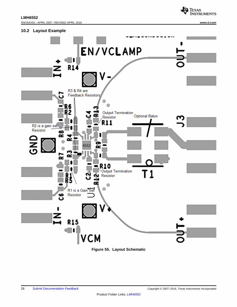
10.1 Layout GuidelinesThe LMH6552 is a very high performance amplifier. In order to get maximum benefit from the differential circuitarchitecture board layout and component selection is very critical. The circuit board must have a low inductanceground plane and well bypassed broad supply lines. External components must be leadless surface mount types.The feedback network and output matching resistors must be composed of short traces and precision resistors(0.1%). The output matching resistors must be placed within 3 or 4 mm of the amplifier as must the supplybypass capacitors. Refer to Power Supply Bypassing for recommendations on bypass circuit layout. Evaluationboards are available free of charge through the product folder on ti.com.
By design, the LMH6552 is relatively insensitive to parasitic capacitance at its inputs. Nonetheless, ground andpower plane metal must be removed from beneath the amplifier and from beneath RF and RG for bestperformance at high frequency.
With any differential signal path, symmetry is very important. Even small amounts of asymmetry can contribute todistortion and balance errors.
28
LMH6552SNOSAX9J –APRIL 2007–REVISED APRIL 2016 www.ti.com
Product Folder Links: LMH6552
Submit Documentation Feedback Copyright © 2007–2016, Texas Instruments Incorporated
10.2 Layout Example
Figure 55. Layout Schematic

29
LMH6552www.ti.com SNOSAX9J –APRIL 2007–REVISED APRIL 2016
Product Folder Links: LMH6552
Submit Documentation FeedbackCopyright © 2007–2016, Texas Instruments Incorporated
10.3 Thermal ConsiderationsThe WSON package is designed for enhanced thermal performance and features an exposed die attach pad(DAP) at the bottom center of the package that creates a direct path to the PCB for maximum power dissipation.The DAP is floating and is not electrically connected to internal circuitry. Compared to the traditional leadedpackages where the die attach pad is embedded inside the molding compound, the WSON reduces one layer inthe thermal path.
The thermal advantage of the WSON package is fully realized only when the exposed die attach pad is soldereddown to a thermal land on the PCB board with thermal vias planted underneath the thermal land. The thermalland can be connected to any power or ground plane within the allowable supply voltage range of the device.Based on thermal analysis of the WSON package, the junction-to-ambient thermal resistance (θJA) can beimproved by a factor of two when the die attach pad of the WSON package is soldered directly onto the PCBwith thermal land and thermal vias are 1.27 mm and 0.33 mm respectively. Typical copper via barrel plating is 1oz, although thicker copper may be used to further improve thermal performance.
For more information on board layout techniques, refer to Application Note 1187 Leadless Lead Frame Package(LLP). This application note also discusses package handling, solder stencil and the assembly process.
10.4 Power DissipationThe LMH6552 is optimized for maximum speed and performance in the small form factor of the standard SOICpackage, and is essentially a dual channel amplifier. To ensure maximum output drive and highest performance,thermal shutdown is not provided. Therefore, it is of utmost importance to make sure that the TJMAXof 150°C isnever exceeded due to the overall power dissipation.
Follow these steps to determine the maximum power dissipation for the LMH6552:1. Calculate the quiescent (no-load) power:
PAMP = ICC* (VS)
where• VS = V+ - V−. (Be sure to include any current through the feedback network if VOCM is not mid-rail.) (1)
2. Calculate the RMS power dissipated in each of the output stages:PD (rms) = rms ((VS - V+
OUT) * I+OUT) + rms ((VS − V−OUT) * I−OUT)
where• VOUT and IOUT are the voltage and the current measured at the output pins of the differential amplifier as if they
were single ended amplifiers and VS is the total supply voltage (2)3. Calculate the total RMS power:
PT = PAMP + PD (3)
The maximum power that the LMH6552 package can dissipate at a given temperature can be derived with thefollowing equation:
PMAX = (150° – TAMB)/ θJA
where• TAMB = Ambient temperature (°C)• θJA = Thermal resistance, from junction to ambient, for a given package (°C/W)• For the SOIC package θJA is 150°C/W• For WSON package θJA is 58°C/W (4)
NOTEIf VCM is not 0V then there is quiescent current flowing in the feedback network. Thiscurrent must be included in the thermal calculations and added into the quiescent powerdissipation of the amplifier.

30
LMH6552SNOSAX9J –APRIL 2007–REVISED APRIL 2016 www.ti.com
Product Folder Links: LMH6552
Submit Documentation Feedback Copyright © 2007–2016, Texas Instruments Incorporated
10.5 ESD ProtectionThe LMH6552 is protected against electrostatic discharge (ESD) on all pins. The LMH6552 can survive 2000 VHuman Body model and 200 V Machine model events. Under normal operation the ESD diodes have no affecton circuit performance. There are occasions, however, when the ESD diodes are evident. If the LMH6552 isdriven by a large signal when the device is powered down the ESD diodes conduct. The current that flowsthrough the ESD diodes either exits the chip through the supply pins or flows through the device, hence a chipcan be powered up with a large signal applied to the input pins. Using the shutdown mode is one way toconserve power and still prevent unexpected operation.

31
LMH6552www.ti.com SNOSAX9J –APRIL 2007–REVISED APRIL 2016
Product Folder Links: LMH6552
Submit Documentation FeedbackCopyright © 2007–2016, Texas Instruments Incorporated
11 Device and Documentation Support
11.1 Device Support
11.1.1 Third-Party Products DisclaimerTI'S PUBLICATION OF INFORMATION REGARDING THIRD-PARTY PRODUCTS OR SERVICES DOES NOTCONSTITUTE AN ENDORSEMENT REGARDING THE SUITABILITY OF SUCH PRODUCTS OR SERVICESOR A WARRANTY, REPRESENTATION OR ENDORSEMENT OF SUCH PRODUCTS OR SERVICES, EITHERALONE OR IN COMBINATION WITH ANY TI PRODUCT OR SERVICE.
11.2 Documentation Support
11.2.1 Related DocumentationFor related documentation see the following:• Leadless Lead Frame Package (LLP), SNOA401
11.2.1.1 Evaluation BoardSee the LMH6552 Product Folder for evaluation board availability and ordering information.
11.3 Community ResourcesThe following links connect to TI community resources. Linked contents are provided "AS IS" by the respectivecontributors. They do not constitute TI specifications and do not necessarily reflect TI's views; see TI's Terms ofUse.
TI E2E™ Online Community TI's Engineer-to-Engineer (E2E) Community. Created to foster collaborationamong engineers. At e2e.ti.com, you can ask questions, share knowledge, explore ideas and helpsolve problems with fellow engineers.
Design Support TI's Design Support Quickly find helpful E2E forums along with design support tools andcontact information for technical support.
11.4 TrademarksE2E is a trademark of Texas Instruments.All other trademarks are the property of their respective owners.
11.5 Electrostatic Discharge CautionThese devices have limited built-in ESD protection. The leads should be shorted together or the device placed in conductive foamduring storage or handling to prevent electrostatic damage to the MOS gates.
11.6 GlossarySLYZ022 — TI Glossary.
This glossary lists and explains terms, acronyms, and definitions.
12 Mechanical, Packaging, and Orderable InformationThe following pages include mechanical, packaging, and orderable information. This information is the mostcurrent data available for the designated devices. This data is subject to change without notice and revision ofthis document. For browser-based versions of this data sheet, refer to the left-hand navigation.
PACKAGE OPTION ADDENDUM
www.ti.com 13-Apr-2016
Addendum-Page 1
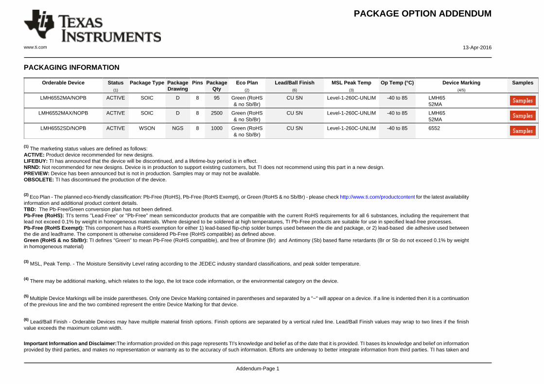
PACKAGING INFORMATION
Orderable Device Status(1)
Package Type PackageDrawing
Pins PackageQty
Eco Plan(2)
Lead/Ball Finish(6)
MSL Peak Temp(3)
Op Temp (°C) Device Marking(4/5)
Samples
LMH6552MA/NOPB ACTIVE SOIC D 8 95 Green (RoHS& no Sb/Br)
CU SN Level-1-260C-UNLIM -40 to 85 LMH6552MA
LMH6552MAX/NOPB ACTIVE SOIC D 8 2500 Green (RoHS& no Sb/Br)
CU SN Level-1-260C-UNLIM -40 to 85 LMH6552MA
LMH6552SD/NOPB ACTIVE WSON NGS 8 1000 Green (RoHS& no Sb/Br)
CU SN Level-1-260C-UNLIM -40 to 85 6552
(1) The marketing status values are defined as follows:ACTIVE: Product device recommended for new designs.LIFEBUY: TI has announced that the device will be discontinued, and a lifetime-buy period is in effect.NRND: Not recommended for new designs. Device is in production to support existing customers, but TI does not recommend using this part in a new design.PREVIEW: Device has been announced but is not in production. Samples may or may not be available.OBSOLETE: TI has discontinued the production of the device.
(2) Eco Plan - The planned eco-friendly classification: Pb-Free (RoHS), Pb-Free (RoHS Exempt), or Green (RoHS & no Sb/Br) - please check http://www.ti.com/productcontent for the latest availabilityinformation and additional product content details.TBD: The Pb-Free/Green conversion plan has not been defined.Pb-Free (RoHS): TI's terms "Lead-Free" or "Pb-Free" mean semiconductor products that are compatible with the current RoHS requirements for all 6 substances, including the requirement thatlead not exceed 0.1% by weight in homogeneous materials. Where designed to be soldered at high temperatures, TI Pb-Free products are suitable for use in specified lead-free processes.Pb-Free (RoHS Exempt): This component has a RoHS exemption for either 1) lead-based flip-chip solder bumps used between the die and package, or 2) lead-based die adhesive used betweenthe die and leadframe. The component is otherwise considered Pb-Free (RoHS compatible) as defined above.Green (RoHS & no Sb/Br): TI defines "Green" to mean Pb-Free (RoHS compatible), and free of Bromine (Br) and Antimony (Sb) based flame retardants (Br or Sb do not exceed 0.1% by weightin homogeneous material)
(3) MSL, Peak Temp. - The Moisture Sensitivity Level rating according to the JEDEC industry standard classifications, and peak solder temperature.
(4) There may be additional marking, which relates to the logo, the lot trace code information, or the environmental category on the device.
(5) Multiple Device Markings will be inside parentheses. Only one Device Marking contained in parentheses and separated by a "~" will appear on a device. If a line is indented then it is a continuationof the previous line and the two combined represent the entire Device Marking for that device.
(6) Lead/Ball Finish - Orderable Devices may have multiple material finish options. Finish options are separated by a vertical ruled line. Lead/Ball Finish values may wrap to two lines if the finishvalue exceeds the maximum column width.
Important Information and Disclaimer:The information provided on this page represents TI's knowledge and belief as of the date that it is provided. TI bases its knowledge and belief on informationprovided by third parties, and makes no representation or warranty as to the accuracy of such information. Efforts are underway to better integrate information from third parties. TI has taken and

PACKAGE OPTION ADDENDUM
www.ti.com 13-Apr-2016
Addendum-Page 2
continues to take reasonable steps to provide representative and accurate information but may not have conducted destructive testing or chemical analysis on incoming materials and chemicals.TI and TI suppliers consider certain information to be proprietary, and thus CAS numbers and other limited information may not be available for release.
In no event shall TI's liability arising out of such information exceed the total purchase price of the TI part(s) at issue in this document sold by TI to Customer on an annual basis.

TAPE AND REEL INFORMATION
*All dimensions are nominal
Device PackageType
PackageDrawing
Pins SPQ ReelDiameter
(mm)
ReelWidth
W1 (mm)
A0(mm)
B0(mm)
K0(mm)
P1(mm)
W(mm)
Pin1Quadrant
LMH6552MAX/NOPB SOIC D 8 2500 330.0 12.4 6.5 5.4 2.0 8.0 12.0 Q1
LMH6552SD/NOPB WSON NGS 8 1000 178.0 12.4 3.3 2.8 1.0 8.0 12.0 Q1
PACKAGE MATERIALS INFORMATION
www.ti.com 13-Apr-2016
Pack Materials-Page 1

*All dimensions are nominal
Device Package Type Package Drawing Pins SPQ Length (mm) Width (mm) Height (mm)
LMH6552MAX/NOPB SOIC D 8 2500 367.0 367.0 35.0
LMH6552SD/NOPB WSON NGS 8 1000 210.0 185.0 35.0
PACKAGE MATERIALS INFORMATION
www.ti.com 13-Apr-2016
Pack Materials-Page 2


www.ti.com
PACKAGE OUTLINE
C
8X 0.30.2
1.5 0.1
8X 0.50.3
2X1.5
1.6 0.1
6X 0.5
0.80.7
0.050.00
B 3.12.9
A
2.62.4
(0.1) TYP
WSON - 0.8 mm max heightNGS0008CPLASTIC SMALL OUTLINE - NO LEAD
4214924/A 07/2018
PIN 1 INDEX AREA
SEATING PLANE
0.08 C
1
4 5
8
PIN 1 ID 0.1 C A B0.05 C
THERMAL PADEXPOSED
9
SYMM
SYMM
NOTES: 1. All linear dimensions are in millimeters. Any dimensions in parenthesis are for reference only. Dimensioning and tolerancing per ASME Y14.5M. 2. This drawing is subject to change without notice. 3. The package thermal pad must be soldered to the printed circuit board for thermal and mechanical performance.
SCALE 5.000

www.ti.com
EXAMPLE BOARD LAYOUT
0.07 MINALL AROUND
0.07 MAXALL AROUND
(1.6)
6X (0.5)
(2.8)
8X (0.25)
8X (0.6)
(1.5)
(R0.05) TYP( 0.2) VIA
TYP
(0.5)
WSON - 0.8 mm max heightNGS0008CPLASTIC SMALL OUTLINE - NO LEAD
4214924/A 07/2018
SYMM
1
4 5
8
SYMM
LAND PATTERN EXAMPLEEXPOSED METAL SHOWN
SCALE:20X
9
NOTES: (continued) 4. This package is designed to be soldered to a thermal pad on the board. For more information, see Texas Instruments literature number SLUA271 (www.ti.com/lit/slua271).5. Vias are optional depending on application, refer to device data sheet. If any vias are implemented, refer to their locations shown on this view. It is recommended that vias under paste be filled, plugged or tented.
SOLDER MASKOPENINGSOLDER MASK
METAL UNDER
SOLDER MASKDEFINED
EXPOSED METAL
METALSOLDER MASKOPENING
SOLDER MASK DETAILS
NON SOLDER MASKDEFINED
(PREFERRED)
EXPOSED METAL

www.ti.com
EXAMPLE STENCIL DESIGN
8X (0.25)
8X (0.6)
6X (0.5)
(1.38)
(1.47)
(2.8)
(R0.05) TYP
WSON - 0.8 mm max heightNGS0008CPLASTIC SMALL OUTLINE - NO LEAD
4214924/A 07/2018
NOTES: (continued) 6. Laser cutting apertures with trapezoidal walls and rounded corners may offer better paste release. IPC-7525 may have alternate design recommendations.
SOLDER PASTE EXAMPLEBASED ON 0.1 mm THICK STENCIL
EXPOSED PAD 9:
82% PRINTED SOLDER COVERAGE BY AREA UNDER PACKAGESCALE:20X
SYMM
1
45
8
SYMM
METALTYP
9

IMPORTANT NOTICE
Texas Instruments Incorporated (TI) reserves the right to make corrections, enhancements, improvements and other changes to itssemiconductor products and services per JESD46, latest issue, and to discontinue any product or service per JESD48, latest issue. Buyersshould obtain the latest relevant information before placing orders and should verify that such information is current and complete.TI’s published terms of sale for semiconductor products (http://www.ti.com/sc/docs/stdterms.htm) apply to the sale of packaged integratedcircuit products that TI has qualified and released to market. Additional terms may apply to the use or sale of other types of TI products andservices.Reproduction of significant portions of TI information in TI data sheets is permissible only if reproduction is without alteration and isaccompanied by all associated warranties, conditions, limitations, and notices. TI is not responsible or liable for such reproduceddocumentation. Information of third parties may be subject to additional restrictions. Resale of TI products or services with statementsdifferent from or beyond the parameters stated by TI for that product or service voids all express and any implied warranties for theassociated TI product or service and is an unfair and deceptive business practice. TI is not responsible or liable for any such statements.Buyers and others who are developing systems that incorporate TI products (collectively, “Designers”) understand and agree that Designersremain responsible for using their independent analysis, evaluation and judgment in designing their applications and that Designers havefull and exclusive responsibility to assure the safety of Designers' applications and compliance of their applications (and of all TI productsused in or for Designers’ applications) with all applicable regulations, laws and other applicable requirements. Designer represents that, withrespect to their applications, Designer has all the necessary expertise to create and implement safeguards that (1) anticipate dangerousconsequences of failures, (2) monitor failures and their consequences, and (3) lessen the likelihood of failures that might cause harm andtake appropriate actions. Designer agrees that prior to using or distributing any applications that include TI products, Designer willthoroughly test such applications and the functionality of such TI products as used in such applications.TI’s provision of technical, application or other design advice, quality characterization, reliability data or other services or information,including, but not limited to, reference designs and materials relating to evaluation modules, (collectively, “TI Resources”) are intended toassist designers who are developing applications that incorporate TI products; by downloading, accessing or using TI Resources in anyway, Designer (individually or, if Designer is acting on behalf of a company, Designer’s company) agrees to use any particular TI Resourcesolely for this purpose and subject to the terms of this Notice.TI’s provision of TI Resources does not expand or otherwise alter TI’s applicable published warranties or warranty disclaimers for TIproducts, and no additional obligations or liabilities arise from TI providing such TI Resources. TI reserves the right to make corrections,enhancements, improvements and other changes to its TI Resources. TI has not conducted any testing other than that specificallydescribed in the published documentation for a particular TI Resource.Designer is authorized to use, copy and modify any individual TI Resource only in connection with the development of applications thatinclude the TI product(s) identified in such TI Resource. NO OTHER LICENSE, EXPRESS OR IMPLIED, BY ESTOPPEL OR OTHERWISETO ANY OTHER TI INTELLECTUAL PROPERTY RIGHT, AND NO LICENSE TO ANY TECHNOLOGY OR INTELLECTUAL PROPERTYRIGHT OF TI OR ANY THIRD PARTY IS GRANTED HEREIN, including but not limited to any patent right, copyright, mask work right, orother intellectual property right relating to any combination, machine, or process in which TI products or services are used. Informationregarding or referencing third-party products or services does not constitute a license to use such products or services, or a warranty orendorsement thereof. Use of TI Resources may require a license from a third party under the patents or other intellectual property of thethird party, or a license from TI under the patents or other intellectual property of TI.TI RESOURCES ARE PROVIDED “AS IS” AND WITH ALL FAULTS. TI DISCLAIMS ALL OTHER WARRANTIES ORREPRESENTATIONS, EXPRESS OR IMPLIED, REGARDING RESOURCES OR USE THEREOF, INCLUDING BUT NOT LIMITED TOACCURACY OR COMPLETENESS, TITLE, ANY EPIDEMIC FAILURE WARRANTY AND ANY IMPLIED WARRANTIES OFMERCHANTABILITY, FITNESS FOR A PARTICULAR PURPOSE, AND NON-INFRINGEMENT OF ANY THIRD PARTY INTELLECTUALPROPERTY RIGHTS. TI SHALL NOT BE LIABLE FOR AND SHALL NOT DEFEND OR INDEMNIFY DESIGNER AGAINST ANY CLAIM,INCLUDING BUT NOT LIMITED TO ANY INFRINGEMENT CLAIM THAT RELATES TO OR IS BASED ON ANY COMBINATION OFPRODUCTS EVEN IF DESCRIBED IN TI RESOURCES OR OTHERWISE. IN NO EVENT SHALL TI BE LIABLE FOR ANY ACTUAL,DIRECT, SPECIAL, COLLATERAL, INDIRECT, PUNITIVE, INCIDENTAL, CONSEQUENTIAL OR EXEMPLARY DAMAGES INCONNECTION WITH OR ARISING OUT OF TI RESOURCES OR USE THEREOF, AND REGARDLESS OF WHETHER TI HAS BEENADVISED OF THE POSSIBILITY OF SUCH DAMAGES.Unless TI has explicitly designated an individual product as meeting the requirements of a particular industry standard (e.g., ISO/TS 16949and ISO 26262), TI is not responsible for any failure to meet such industry standard requirements.Where TI specifically promotes products as facilitating functional safety or as compliant with industry functional safety standards, suchproducts are intended to help enable customers to design and create their own applications that meet applicable functional safety standardsand requirements. Using products in an application does not by itself establish any safety features in the application. Designers mustensure compliance with safety-related requirements and standards applicable to their applications. Designer may not use any TI products inlife-critical medical equipment unless authorized officers of the parties have executed a special contract specifically governing such use.Life-critical medical equipment is medical equipment where failure of such equipment would cause serious bodily injury or death (e.g., lifesupport, pacemakers, defibrillators, heart pumps, neurostimulators, and implantables). Such equipment includes, without limitation, allmedical devices identified by the U.S. Food and Drug Administration as Class III devices and equivalent classifications outside the U.S.TI may expressly designate certain products as completing a particular qualification (e.g., Q100, Military Grade, or Enhanced Product).Designers agree that it has the necessary expertise to select the product with the appropriate qualification designation for their applicationsand that proper product selection is at Designers’ own risk. Designers are solely responsible for compliance with all legal and regulatoryrequirements in connection with such selection.Designer will fully indemnify TI and its representatives against any damages, costs, losses, and/or liabilities arising out of Designer’s non-compliance with the terms and provisions of this Notice.
Mailing Address: Texas Instruments, Post Office Box 655303, Dallas, Texas 75265Copyright © 2018, Texas Instruments Incorporated

![274-824-6 EINECS - MASTER INVENTORY 274-850-8 274-824-6 ... · 274-824-6 EINECS - MASTER INVENTORY 274-850-8 1 EC_2748246_2759237 274-824-6 70729-60-1 etyl-[2-[etyl(3-metylfenyl)amino]fenyl]karbamát](https://img.pdfslide.us/doc/110x75/5e39c5c3e9db7d2db32094c4/274-824-6-einecs-master-inventory-274-850-8-274-824-6-274-824-6-einecs-master.jpg)


![[XLS] · Web view317 317 317 317 315 94 315 94 86 86 86 426 426 426 316 239 316 239 317 317 317 315 94 315 94 315 315 315 315 426 274 136 274 136 274 136 274 136 274 188 274 188 274](https://img.pdfslide.us/doc/110x75/5abaa3447f8b9a567c8bbc31/xls-view317-317-317-317-315-94-315-94-86-86-86-426-426-426-316-239-316-239-317.jpg)