Embed Size (px)
Citation preview
Organized by
http://vlsi-india.org/vsi/
To promote applications and research related to all
aspects of VLSI in India
Sponsored by
Chitkara University
Chandigarh http://www.chitkara.edu.in/
Texas Instruments India http://www.ti.com/
In cooperation with
IEEE Chandigarh Subsection
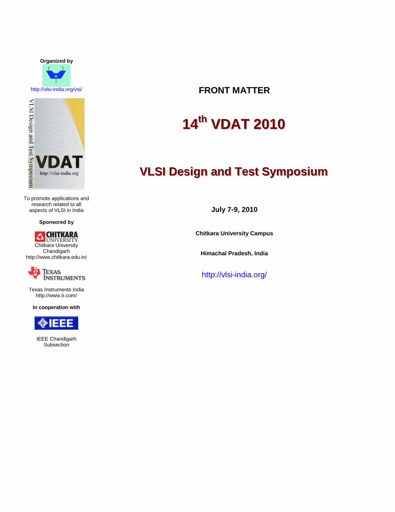
FRONT MATTER
111444ttthhh VVVDDDAAATTT 222000111000
VVVLLLSSSIII DDDeeesssiiigggnnn aaannnddd TTTeeesssttt SSSyyymmmpppooosssiiiuuummm
July 7-9, 2010
Chitkara University Campus
Himachal Pradesh, India
http://vlsi-india.org/
Message from the General Chairs
C.P. Ravikumar Mohit Chitkara
Dear Colleague,
It is our pleasure to welcome you to the 14th VLSI Design and Test Symposium (VDAT 2010). After many years, VDAT has returned to the northern region. A proposal about holding VDAT in Chandigarh was made more than a year ago by Chitakara University. Chandigarh is a beautiful city, the personal favorite of our late Prime Minister Pandit Jawaharlal Nehru. Chandigarh is the home for the famous rock garden built by Nek Chand Saini. We invite you to visit this awe-inspiring place where waste materials and rocks have been ingeniously assembled into beautiful works of art. One cannot help but think of the waste that we generate today, in the form of floppy disks, CDs, batteries, and even cell phones and computers. As new technology is ushered in, older gadgets are discarded. We must derive inspiration from Nekchand’s Rock Garden and think seriously about how we deal with electronic waste.
The venue for VDAT 2010 is the Chitkara University campus, located about 25 Km from Chandigarh. We hope you will enjoy the peaceful location in the foothills of Shivalik Hills. We hope that you will enjoy the hospitalities offered by Chitkara University, which was set up by Prof. Chitkara and his wife Dr. Madhu Chitkara to offer high-quality education. We also believe you will enjoy the technical program that has been put together by the technical program committee of VDAT 2010. There are three parallel tracks of tutorials on July 7. We have keynote talks and invited talks by stalwarts of the VLSI profession. A panel discussion will set your mind in motion. More than 40 carefully selected technical papers will offer you a great learning experience of recent advances in VLSI/Embedded System Design and Test. A research scholar forum has been organized to encourage young researchers in Indian Universities to present their recent research findings. There is also ample scope for industry-academia interaction. Please use the networking opportunities to strike new friendships and collaborations.
An event of this nature cannot be organized without the cooperation of many organizations and hardwork from a number of individuals. It is hard for us to enumerate all the names. We thank the VLSI Society of India for sponsoring the event. We thank Texas Instruments and Chitkara University for their generous support to the event. In particular, we are grateful to Dr. Bobby Mitra, Dr. Ashok Chitkara, and Dr. Madhu Chitkara for their support. We thank IEEE Chandigarh Subsection and the IEEE Student Chapter of Chitkara University for their cooperation. We thank Prof. Vishwani Agrawal (Steering Committee Chairman) and Dr. Bobby Mitra (President of VLSI Society of India) for their constant encouragement. We gratefully acknowledge the help from the members of the technical committee and the reviewers who spent their valuable time reviewing the submitted papers. We thank the keynote speakers, invited speakers, session chairs, and panelists for honoring our invitation. We are grateful to Prof. Rajnish Sharma, Local Organization Chair, the faculty members of Chitkara University, and the entire team of volunteers who have spared no effort to make VDAT 2010 a great experience for the participants. We thank Prof. Archana Mantri, who along with Prof. Rajnish Sharma and other faculty colleagues, made the proposal to bring VDAT to Chandigarh. Last, but not the least, we thank you for taking part in VDAT as an author, presenter, or delegate. We hope that your support to VDAT will continue in the future.
You will be happy to know that the venue of VDAT 2011 is now decided. Pune, hailed as the Oxford of the East, will play host to the 15th VLSI Design and Test Symposium during July 7-9, 2011. You will find a copy of the Call for Papers for VDAT 2011 in your registration kit. Please mark your calendars and plan to attend the event.
Regards
C.P. Ravikumar and Mohit Chitkara
VDAT2010 Organizing Committee
General Chairs
C.P. Ravikumar, Texas Instruments India
Mohit Chitkara, Chitkara University
Local Organization Chair
Rajnish Sharma, CIET, Chandigarh
Finance Chair
S.R. Gopal Naidu, Texas Instruments India
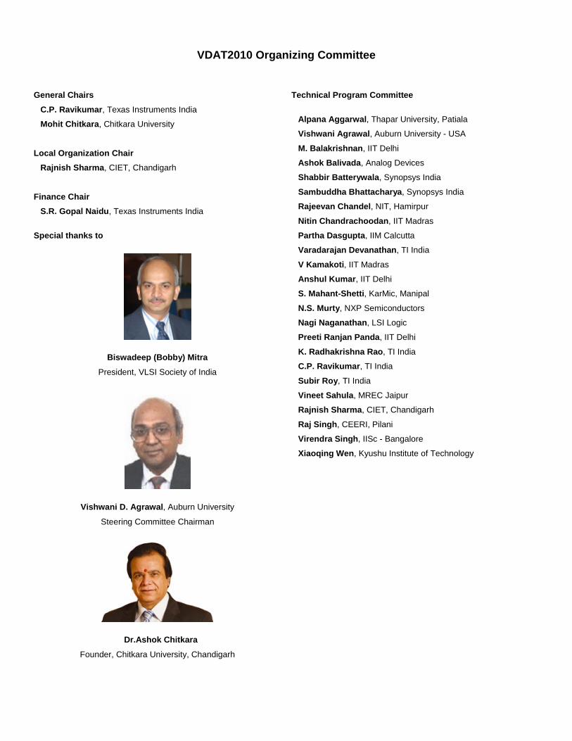
Special thanks to
Biswadeep (Bobby) Mitra
President, VLSI Society of India
Vishwani D. Agrawal, Auburn University
Steering Committee Chairman
Dr.Ashok Chitkara
Founder, Chitkara University, Chandigarh
Technical Program Committee
Alpana Aggarwal, Thapar University, Patiala
Vishwani Agrawal, Auburn University - USA
M. Balakrishnan, IIT Delhi
Ashok Balivada, Analog Devices
Shabbir Batterywala, Synopsys India
Sambuddha Bhattacharya, Synopsys India
Rajeevan Chandel, NIT, Hamirpur
Nitin Chandrachoodan, IIT Madras
Partha Dasgupta, IIM Calcutta
Varadarajan Devanathan, TI India
V Kamakoti, IIT Madras
Anshul Kumar, IIT Delhi
S. Mahant-Shetti, KarMic, Manipal
N.S. Murty, NXP Semiconductors
Nagi Naganathan, LSI Logic
Preeti Ranjan Panda, IIT Delhi
K. Radhakrishna Rao, TI India
C.P. Ravikumar, TI India
Subir Roy, TI India
Vineet Sahula, MREC Jaipur
Rajnish Sharma, CIET, Chandigarh
Raj Singh, CEERI, Pilani
Virendra Singh, IISc - Bangalore
Xiaoqing Wen, Kyushu Institute of Technology

VDAT2010 Reviewers
Jais Abraham Saif Abrar
Venkatesh Acharya Alpana Agarwal Vishwani Agrawal
Akhtar W. Alam K. Anand Venkataraman Anantharaman
N. Balaji M. Balakrishnan Ashok Balivada
Dr. Gaurab Banarjee Swapna Banerjee Shabbir Batterywala
M.S. Bhat Sambuddha Bhattacharya S C Bose
Rajeevan Chandel Nitin Chandrachoodan Santanu Chattopadhyay
Salil Chellapan Vishal Dalal Sudeb Dasgupta
Parthasarathi Dasgupta Sankar Dasiga Utpal Desai
Varadarajan Devanathan Bilas Datta Nagendra Dwarakanath
Salil Gadgil Partha Garai Hitesh Garg
Manoj Gaur G Girishankar ANU GUPTA
Niraj Gupta Ajit Gupte
C Guruprasad Rohini Hongal
Aminul Islam Bhooshan Iyer Rekha James
P Jayalakshmi Dr. Bhavana Jharia Supreet Joshi
Sunilduth K Kanigere Gautam Kapila Rajib Kar
Sunil Kasanyal Samvit Kaul Manjit Kaur
Mandeep Kaur Rajwinder Kaur Rajesh Kedia
Aman Kokrady Nagendra Krishnapura Giten Kulkarni
Satyendra Kumar Virender Kumar Anshul Kumar
Vijay Kumar Venkateswaran Mahadevan S. Mahant-Shetti
Ramakrishnan Mandiram Sanjeev Manhas Sujan Manohar
Vinod Menezes Thenappan Meyyappan Shivshankar Mishra
Sunil Misra Raj Mitra Poornima Mohanachandran
Sunil Moolakkaran Venugopala Mudumbu
Debdeep Mukhopadhyay Nagavolu Murty
MJ Abdul Muthalif Mohankumar N Nagi Naganathan
Chandrakant Nalage Prakash Narayanan Dharmaray Nedalgi
Vaibhav Neema Ajit Panda Preeti Ranjan Panda
Sangeeta Panigrahy Rubin Parekhji Chetan Parikh
Amit Patra Rajendra Patrikar Kolin Paul
Sasikumar Periasamy Sakthivel Periyasamy Milind Phadtare
Sanjay Prajapati Sudheer Prasad Y.A. Prithvi
Karthik Rajagopal Prasad Rajasekhar Dr.Manjunath Ramachandra
K. Radhakrishna Rao C.P. Ravikumar Sudhakar Reddy
Venugopal Reddy Rajendra Rewatkar Subir Roy
Shubhajit Roy Chowdhury Chirasree RoyChaudhuri Prabir Saha
Hiranmay Saha Vineet Sahula
Santosh Salunkhe Sankar Sarma
Yogesh Save Ridhi Seth Vishal Shah
Malav Shah Kalpesh Shah Dinesh Sharma
Rajnish Sharma G Dharne Shivraj Biplab Sikdar
Biju P. Simon Raj Singh Adit Singh
Virendra Singh Saurbh Srivastava P R Suresh
Ganesan Thiagarajan Aravinda Thimmapuram Tessil Thomas
Jayanth Thyamagundalam Naveen Tiwari H Udayakumar
Dr.Narendranath Udupa Dr.Shyam Vasudev Shriram Vasudevan
Kamakoti Veezhinathan Srinivasan Venkataraman Srinivasan Venkataramanan
B Venkataramani Ramakrishnan Venkatraman Aishwarya Vijayanand
Nita Vishwakarma V. Visvanathan Xiaoqing Wen
Pushpendra Yadav
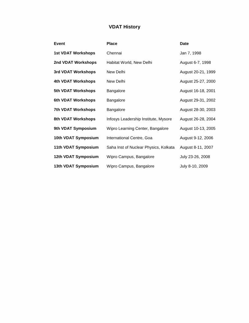
VDAT History
Event Place Date
1st VDAT Workshops Chennai Jan 7, 1998
2nd VDAT Workshops Habitat World, New Delhi August 6-7, 1998
3rd VDAT Workshops New Delhi August 20-21, 1999
4th VDAT Workshops New Delhi August 25-27, 2000
5th VDAT Workshops Bangalore August 16-18, 2001
6th VDAT Workshops Bangalore August 29-31, 2002
7th VDAT Workshops Bangalore August 28-30, 2003
8th VDAT Workshops Infosys Leadership Institute, Mysore August 26-28, 2004
9th VDAT Symposium Wipro Learning Center, Bangalore August 10-13, 2005
10th VDAT Symposium International Centre, Goa August 9-12, 2006
11th VDAT Symposium Saha Inst of Nuclear Physics, Kolkata August 8-11, 2007
12th VDAT Symposium Wipro Campus, Bangalore July 23-26, 2008
13th VDAT Symposium Wipro Campus, Bangalore July 8-10, 2009
Design of 6-bit Folding & Interpolating ADC using Low Power Folding Amplifier
Shruti Oza1, N.M. Devashrayee2
Abstract
Folding and interpolating A/D converters have been shown to be an effective means of digitization of high bandwidth signals at intermediate resolution. The paper focuses on design of 6-bit folding & interpolating ADC using low power folding amplifier. This paper seeks to use folding amplifier to produce more than one zero-crossing points to reduce required number of comparators. The converter is designed using novel low power folding amplifier with folding factor=4 and 8. The folding amplifier is used in the design of coarse and fine converter both. To reduce the power consumption, encoder based on XOR-OR logic is used. The design is implemented using 0.18µm technology at 3.3 V supply voltage. Keywords: Comparator, Encoder, Folding Amplifier, Folding & Interpolating ADC, Interpolation, Low Power.
1. Introduction Analog-to-digital converter is one of the most important building blocks to transform analog signals to digital signal process systems. For high-speed application, the fully flash ADC is widely used. Flash ADC has the highest conversion rate because of its fully parallel architecture. It is found that N-bit
flash ADC needs 2 N- 1 comparators, which consume large power and occupy
area [1, 8]. The attractiveness of folding and interpolating ADCs lies in its clever solution to the flash ADC’s problem of an exponential increase in the number of comparators for each additional bit of resolution. Folding architecture is an alternative approach to reduce the complexity of flash ADC and still keep high conversion rate [2]. Before the outputs of the preamplifiers are fed into comparators, folding amplifiers are inserted. The folding amplifier can produce more than one zero-crossing point. Folding amplifier combines the outputs of several preamplifiers and generates folding waveforms, which contains
1 EC Department, Kalol Institute of Technology & Research Centre,
Nr. Highway, Kalol-382721, Gujarat, [email protected]
2 EC Department, IT-Nirma University of Science & Technology
S.G. Road, Nr. Chharodi, Ahmedabad, [email protected]
1
CMOS Transconductance Elementfor Low-Frequency Applications
Dr. Venkatesh AcharyaTexas Instruments, Dallas
Abstract
A negative feedback technique eliminates the need for ratioing transistors to implement the cross-coupled Quadcell [1]. Output current of this transconductance containsboth odd and even component of the input voltage.Unwanted common-mode component of the output current can becompletely removed by selective even feedbacktechnique. Simulation results are provided to prove that this selective feedback doesn’t attenuate or distort the linearcomponent of output current. A transonductance element designed in 0.18µm process can be used till 100MHzsignal without distorting the signal more than 0.35% linearity.
Index Terms
Analog, Transconductance element, CMOS Quad, negative feedback, selective even feedback
I. INTRODUCTION
L INEAR transconductors are essential building blocks for the design of integrated active filters. The symmetricdifferential pair is the most popular transconductance element. The nonlinearity in itsv− i transfer character-
istics can be reduced by using two asymmetrical differential pairs connected cross-coupled. This cell is known asQuad [2]. Due to asymmetry, the Quad generates two useful output currents. First component is the odd functionof the applied voltage and other component has even characteristics [f(x) is an odd function iff(−x) = −f(−x)andf(x) is even iff(−x) = f(x)]. Linearity of the CMOS Quad can be further improved by selectively isolatingthe even component of the output current and feeding it back to its tail current [3]. This also removes the evencomponent completely from the output current.
Asymmetry needed to implement the CMOS can be realized without ratioing the input devices by negativefeedback technique [1]. In this paper selective even feedback technique is applied to this negative feedback Quadand even component is completely removed from the output. Simulation results obtained using the 0.18µm TSMCprocess shows the linearity that can be obtained. Also distortion of this element across different frequenciesare provided to indicate the frequency range over which thiscircuit can be employed for continuous-time filterapplications.
II. CMOS QUAD
When two identical skewed pairs, transposed with respect toeach other and connected in parallel it forms a thewell-known Quad [2]. Two asymmetric differential-pairs(M1,M2) and(M3,M4) form the CMOS Quad as shownin Fig. 1. The widths of the transistors in each pair are scaled in the ratio of1 : n to create a skew as shown.The differential input-voltagev appears in opposite polarities for the two pairs. Each pair is biased by a currentsink of value(n + 1)I. In a symmetric differential pair, the incremental output currents are an odd-function [4] ofthe input voltage whereas the skewed pair generates both oddand even components. By subtraction of the draincurrents ofM4 andM2 we can isolate the odd component and by addition of the drain currents ofM1 andM3,we get a purely even-function. The odd component of the output current gets more and more linear as the valueof n increases. This favorable result comes with the cost increased power consumption.
Fig. 2 shows the smart way of implementing the Quad which emulates the performance of the Quad with verylarge value ofn. This is achieved by a strong negative feedback. In this casewidth of transistorsM1−4 is equal. Ityields, the same bias current in both the transistors. The feedback provided by the transistorM5(M6) ensure theconstant current operation for the transistorM4(M2).The bias current of the transistorM4 is fixed toI. It leads tothe bias current of the transistorM3 is equal toI and bias current through the transistorM5 equal toIB − 2I. The
Design of a 10-bit, 5 Ms/S Pipelined ADC for CMOS Image Sensor
Kanhu Ch. Behera1, M.Santosh2, S.C.Bose3
Abstract:
In this paper design of a 10bit, 5MS/s pipelined ADC suitable for chip level integration of CMOS image sensors has been attempted. The designed pipeline ADC is simulated in 3.3 V, double poly, triple metal 0.35 µm Austria Microsystems process. The maximum DNL and INL of the designed pipeline ADC are -1/+0.5LSB and -2.5/+1.75LSB respectively. The dynamic input range of the ADC is 3 V. The designed ADC eliminates the need of front end S/H circuit, thereby reducing the chip area and power. The designed pipeline ADC consumes a power of 40mW and chip area of only 0.49 mm2. The offset cancellation of the S/H circuit and the Multiplying Digital-to-Analog circuit (MDAC) are done by the use of a simple offset cancellation switch.
Index: CMOS image Sensor, pipeline, ADC, flip-around, Sample-and-Hold
1. Introduction:
Modern multimedia applications starting from camcorder to video digital cameras demand the integration of ADCs and CMOS-based image sensor on a single chip. CMOS-based image sensor consists of a matrix of pixels depending on the required resolution of the image. There are different approaches of pixel implementation in CMOS technology such as passive pixel, active pixel etc. [1]. The development of active pixel sensors made the integration of image sensor and the read out circuit possible on a single chip i.e. camera-on-chip [1]. Due to modern CMOS technology the integration of image sensor along with the read out circuit leads to low cost, low power and low voltage camera-on-chip. Camera-on-chip requires on chip analog-to-digital converter with 8-10 bit resolution, less power consumption, and with lesser silicon area. The minimum required resolution of on-chip ADC is 8-bit with differential nonlinearity and integration nonlinearity as low as possible so as not to introduce distortion in the image. The power consumption of the ADC should be less than 100mW to avoid the introduction of hot spot [1]. There are different approaches for on chip integration of ADC like pixel level, column parallel level and finally the chip level [1-2]. Pixel level approach requires low speed ADC as each pixel is associated with a separate ADC, where as column parallel approach require medium speed ADCs as each ADC is allocated for one or several columns of pixels, But the chip level approach needs only one high speed ADC for the whole pixel array[1]. Due to reduced mismatch concerns, chip level integration is preferred over the other two types of integration [2]. For image processing application the on chip ADC must support a range of video rate of 0.92 MS/s for a 320x288 format sensor operating at 10 frames/s to 55.3 MS/s for a 1280x720 format sensor operating at 60 frames/s[1]. Requirement of such kind of video 1, 2, 3 Central Electronics Engineering Research Institute, Pilani (CSIR)
A Sensitivity Analysis Based Approach to
Statistical Parameter Estimation of Analog
Circuits
Amitava Banerjee1, Arnab Khawas
2, Amit Patra
3
and Siddhartha Mukhopadhyay4
Abstract
Process variations have increased significantly with scaling technologies. This
has led to deviations in analog circuit performance from their expected values.
For submicron design, it is essential to simulate the circuit at all process
corners for yield verification. In this work we develop a methodology based
upon a sensitivity analysis of transistor mismatch to circuit performance for
statistical design parameter estimation. This methodology has been implemented
in a CAD tool. With the objective of rapid simulation, the performance of a
circuit under process variation can be effectively estimated using the tool while
achieving a significant speedup over conventional Monte Carlo methods.
Keywords: Monte Carlo, Common Mode Rejection Ratio, Standard Deviation,
Correlation Coefficient, Sensitivity-Covariance Analysis.
1. Introduction
In modern submicron design technology, process variation induced transistor
mismatch has become a highly challenging factor for analog design. Magnitude
of mismatch increases along with the reduced device feature size. MOS
transistor mismatch is generally represented by threshold voltage mismatch
(∆VT0), oxide thickness mismatch (∆tox), mobility mismatch (∆µ) and body
factor mismatch (∆γ). Threshold voltage mismatch and current factor mismatch
∆β (combination of ∆tox and ∆µ) are correlated and can be fitted by polynomials
from mismatch measurement data on test chips. For many years there has been
research on modeling device level mismatch that causes parametric faults. The
idea and procedure of device level mismatch modeling was first introduced by
Pelgrom [1]. Most of the large signal mismatch models are built upon square
law device characteristic. In [2]–[5] different MOS mismatch models based on
parametric test data have been introduced. The objective of those research works
is to predict the variance of drain current by complex polynomials of W (width)
and L (length). A BSIM3V3 model for standard deviation of saturation current
expression from submicron to strong inversion regime is given in [6]. All the
predicted models are integrated with SPICE simulators. As suggested in [7], [8]
a simple statistical MOS transistor model is considered, where unlike the usual
1 National Semiconductor, Bangalore, India, [email protected],
2 Department of EE, IIT, Kharagpur, India, [email protected],
3 Department of EE, IIT, Kharagpur, India, [email protected],
4 Department of EE, IIT, Kharagpur, India [email protected]
1
A Short Tutorial on Analog Layout Challenges
in Deep Submicron Technologies
Vishwanath Hanchinal 1 and Vijay Mundlapudi 1
ABSTRACT
As the semiconductor physics is driving to more and smaller geometries, the challenges are growing for the designers and layout engineers to design in these technologies. Many of new effects in these advanced technologies are making the job of Analog Design/Layout more complex while designing in these technologies. These effects start to kick in from 90nm technology, but pose a real challenge in designs for 45nm and beyond. The intent of this tutorial is to showcase the cause and significance of the deep sub-micron effects on the design/layout of analog circuits which may cause failure in silicon if not provided enough attention. Also proposed are some guidelines which designers should keep in mind while designing circuits in these technologies. Keywords (Index): STI, WPE, Parasitic effects, poly proximity effect 1. INTRODUCTION The formation of deep p- and n- wells using high-energy implantation has become an integral part of CMOS technology process flow. The high energy and high dose implantation (introduced to suppress parasitic bipolar gain for latch-up protection) into the cleared area of a thick photo-resist mask generates etrograde profiles. These profiles have a relatively high peak concentration usually at the depth of approximately 1 micron and a very low surface concentration. From the first glance this process achieves its primary goal to isolate NFETs from PFETs without affecting surface areas where the transistors are formed. Unfortunately for both technology and circuit designers, this relatively simple process step brings about an unwanted Well Proximity Effect (WPE) exhibited by a strong dependence of threshold voltage Vt on transistor location and even orientation within the well. Significant proximity effects are well Proximity Effect (WPE), STI stress (LOD), parasitic effects and Poly Proximity effect. 1 NXP Semiconductors India Pvt Ltd, Bangalore; Email: [email protected] Email: [email protected]
Asynchronous ADC Using
Novel Asynchronous Subranging Scheme
Anita Deshmukh1, Ravi Patil2,
Raghavendra Deshmukh3 and Rajendra Patrikar
4
Abstract
In this paper we propose the development of a novel subranging scheme for
Asynchronous Analog to Digital Converters (A-ADC). An innovative
subranging method using dynamic characteristic of comparator has been proposed. Time domain representation of comparator input voltage
difference is used to quantize the input. It improves the resolution of A-ADC
without increasing the complexity of analog blocks like Digital to Analog
Converter (DAC). The prototype is designed using standard 90nm CMOS
technology and simulated using Synopsys HSpice for hardware resolution of
6 bits. A-ADC uses non-uniform sampling and provides 4 bits from coarse
conversion. Subranging scheme uses vertical structured ADC and window
amplifier. It provides 2 bits from fine conversion. Current design has loop
delay of 56nsec with average power 190µW and SNR equal to 38dB which
offers significant improvement over reported schemes. Major contribution
of this work is a novel Asynchronous Subranging Scheme.
Keywords (Index): Asynchronous Analog to Digital Converter (A-ADC),
subranging, comparator, non-uniform sampling.
1.Introduction
Analog-to-Digital Converter (ADC) is a key design block of current
technology for implementing digital signal processing scheme. ADCs are
critical to design [1] respecting all the constraints like low power, reduced
size, low noise, less conversion time with low cost. A standard ADC
technology based on Nyquist criteria usually results in redundant data
samples. For many real life signals it digitizes much more data than is actually useful. This leads to unnecessary increase in circuit activity and
power consumption. An asynchronous ADC design without any global
clock [2][3] uses non-uniform sampling of analog input signal. It is used to
improve performances of Nyquist ADCs. This design style offers
advantages like reduced activity, reduced hardware, low power
consumption, electromagnetic compatibility, immunity to metastability, high
speed, robustness to technology and environment variations.
The proposed novel subranging scheme is implemented for an existing A-
ADC architecture [3]. It provides the technique to trade-off conversion
speed with improved architecture. It provides considerable reduction in loop delay. This implementation takes an advantage of dynamic characteristic of
comparator and asynchronous design style. Asynchronous design is
1 Department of ECE,VNIT Nagpur. email: [email protected]
2 email: [email protected]
3 Department of ECE,VNIT Nagpur. email: [email protected]
4 Department of ECE,VNIT Nagpur. email: [email protected]
A Technology Specific Approach to Reduce Leakage
Sambhu Nath Pradhan Subhadip Kundu Santanu Chattopadhya
KIIT University, Bhubaneswar-751024 IIT-Kharagpur-721302, India
[email protected] [email protected] [email protected]
Abstract: As technology scales down below submicron level, leakage power is emerging as a dominant part in the overall
power equation. This paper aims at reducing standby leakage in a technology specific manner by using various
avenues like input vector control, cell replacement etc. The increase in delay due to the usage of high-threshold
devices is tackled via upsizing. It has been shown that upto 95% saving in leakage can be achieved. As a by-product,
it also reduces the dynamic power upto about 9.5%.
1. Introduction With the advancement in VLSI process technology, the complexity of the circuits packed into a single IC is
going up by leaps and bounds. Now it is quite common to have more than 100M transistors on a single chip. The
possibility of accommodating such a huge number of transistors opens up the opportunity to design a complete
system as a single IC. Such a complex design introduces newer challenges in the front of power consumption.
Supply voltage and device dimensions are often scaled to increase the packaging density and reduce the dynamic
power (as dynamic power is proportional to the square of the supply voltage). Transistor threshold voltage also
needs to be scaled to achieve the required level of performance. Unfortunately, such scaling increases the leakage
current. Due to the exponential nature of leakage current, in the subthreshold regime, leakage current can no longer
be ignored. The International Technology Roadmap for Semiconductors (ITRS) projects an exponential increase in
the leakage power with miniaturization of devices. Leakage power for 0.1um technology is 25% of that of the active
power. As the technology drops below 65 nm feature size, leakage is expected to exceed the total dynamic power
[1]. On the other hand, in a complete system, it is very much unlikely that all parts of it will always be active and
thus consume dynamic power. A major share of power consumption is often due to the idle components, known as
stand-by leakage power. There are three important leakage mechanisms [9] — Subthreshold leakage, Gate Direct
Tunneling leakage and Junction Band-To-Band-Tunneling leakage. Thus, there has been considerable amount of
work reported in the literature to reduce this stand-by leakage power. In the following, we reviewed some of them
[2, 3, 4].
1.1 Leakage control using body-biasing
In standby mode, the body Vb of a NMOS device is biased to a voltage lower than the ground potential in order to
increase its threshold voltage. Thus, the leakage current is reduced. In the active mode, the body is biased to ground
to attain the normal Vth value. Thus, the speed of the NMOS device remains unaltered. Similarly, the PMOS device
is biased to a voltage higher than Vdd in the standby mode, to reduce leakage. Two examples of body biasing
techniques are the Variable Threshold CMOS (VTCMOS) and the Dynamic Threshold CMOS (DTCMOS)
1.2 Leakage control using Multi-Vth design
There are two main ways to utilize the multi-threshold CMOS technology to manage leakage power during the
standby mode while maintaining performance in the active mode:
(i) Using high-Vth sleep transistors (Dynamic approach)
(ii)Embedded multi-Vth CMOS design (Static approach)
However, the usage of sleep transistors is not encouraged due to higher area overhead, extra latches, higher
impedance and sizing problems. The multi-threshold design approaches [5, 6, 7, 8] aim at replacing some transistors
on the non-critical path by their higher threshold version. While the works in [5, 6, 7] attempt delay-constrained
design (optimizing power), [8] attempts a power-constrained design to optimize delay. Both the approaches are
library based, in the sense that the library contains two types of cells, one with low Vth and the other with high Vth. A
cell not present in the critical path may get replaced by the high Vth version of the cell to reduce leakage. On the
other hand, the works presented in [9, 13, 14] assign high or low threshold values to individual transistors within a
cell to achieve better control over the leakage saving procedure. However, such schemes require a large number of
cell variants which translates to a large library and characterization effort.
Other transistor level Vth assignment approaches are [10, 11, 12, 21, 22] which start with nominal Vth assigned to all
transistors and assigns low Vth iteratively to timing-critical transistors. These methods combine transistor sizing and
Vth assignment. The enumeration based approach proposed in [10] quickly grows in space and runtime requirements
as the input size increases. The approach neglects the effect of Vth assignment on capacitance. A sensitivity-based
downsizing that begins with low Vth assigned to all transistors and assigns nominal Vth to non-critical transistors is
presented in [12]. As the state probabilities of nodes in a circuit tend to be skewed, i.e., they have either low or high
Novel Low Power Multipliers using
Bypassing Schemes
P.Saravanan1, S.Brinda
2
Abstract
In the fast growing communication field, requirements for low
power designs are increasing to reduce the power losses. Multiplier is an
arithmetic circuit that is extensively used in common DSP and
communication applications. This paper presents circuit techniques for
CMOS low-power area-efficient multiplier design by taking advantage of
bypassing method. In an array multiplier, power saving comes from
bypassing signals along those adder rows or columns, corresponding to zero
bits in the multiplier or in the multiplicand term. Spurious signal switching
activities can then be eliminated when bypassing occurs. In an attempt to
reduce the power dissipation further, the proposed scheme skips redundant
signal transitions by replacing most of the partial products with their
corresponding input signals without affecting the functionality. The
proposed column bypassing multiplier is achieved to reduce the power
consumption by 23.1%, whereas existing column bypassing method shows
only 9.5% power reduction. The area overhead of the proposed design is
roughly 6.5% for column-bypassing multiplier, while that of existing
column-bypassing multiplier is 23%. All the above figures are the power
saving and circuit overheads when compared to conventional 16-bit array
multiplier. All simulations of the proposed multiplier have been carried out
in 130nm CMOS technology.
Keywords: Multiplier, low power, Bypassing scheme.
1. Introduction
Most Digital Signal Processor (DSP) systems incorporate a
multiplication unit to implement algorithms such as convolution and
filtering. In many DSP algorithms, the multiplier lies in the critical delay
path and ultimately determines the performance of the algorithm. However,
the demand for high-performance portable systems incorporating
multimedia capabilities has elevated the design for low-power to the
forefront of design requirement in order to maintain reliability and provide
longer hours of operation.
In recent years, many attempts have been reported in literature about
improvement in multipliers. The multiplier [1] with the structure of binary
tree uses a new design of full adder to minimize the power dissipation.
------------------------------------------------------------------------------------------------- 1Lecturer, ECE Dept., PSG College of Technology, Coimbatore; [email protected]
2Junior Telecom Officer (Trainee), BSNL, Tamilnadu; [email protected]
Robust and Self-Adaptive Power Reduction Techniques for FIFO Buffers
Salil Gadgil1, Senthilkannan Chandrasekaran2, Anuja
Bagdi3
Abstract
CMOS technology node is shrinking, making leakage power an increasing contributor in power consumption. FIFO (First-In-First-Out) designs are widely used in SOC (system-on-chip), NOC (network-on-chip) architectures. The memories occupy a significant portion of area in a FIFO, making it a big contributor in power dissipation of a FIFO. This paper explains an innovative, robust and self adaptive algorithm for reducing both - dynamic and leakage power dissipated inside a FIFO using retention and power down modes of the memories. Algorithms, implementation gains and penalties of the proposed method are discussed in this paper. Keywords: Low Power Design, Memory Architecture. 1. Introduction
Technology node is shrinking over the years (135nm � 90nm �
65nm � 45nm � 28nm) and the leakage current per gate of a node is increasing when compared to the previous nodes [1,2]. Components of power dissipation and power reduction techniques have been explained in [3,4]. FIFO components are widely implemented to buffer data [5]. Sizing of FIFO [6] is an important task during the architecture specification cycle. FIFO designs are getting bigger as the amount of buffering required is increasing [7] thereby impacting the power dissipation. In this paper we propose a self-adaptive algorithm for reduction of dynamic and leakage power inside FIFO memories using the memory retention and memory power down features of the memory. We propose an effective and scalable algorithm that uses the power down and retention capabilities of the memories. We also show that the implementation of this algorithm results in a power reduction of about 15 - 50% of the total FIFO power dissipation under different scenarios.
The rest of this paper is organized as follows: Section 2 explains the motivation behind the work. Section 3 details the prior art and related work. Section 4 explains the proposed scheme, associated algorithms and hardware design. Section 5 discusses the results and gains/penalties using the proposed scheme. Section 6 finally concludes the paper.
1 Salil Gadgil, [email protected] 2 Senthilkannan Chandrasekaran, [email protected] 3 Anuja Bagdi, [email protected] All at Texas Instruments Pvt Ltd, India Bangalore
Design of Static Latch-based
Comparators using Power
Constrained Optimization
Purushothaman A, Chetan D. Parikh
Abstract
Comparators are basic building blocks in many analog and mixed-signal systems. Design and synthesis of comparator architectureslargely remains an analog designers art. In this work, we presenta systematic methodoloy for designing a latch-based comparator ar-chitecture using constrained optimization. The circuit is optimizedfor power, under constraints on gain, dimensions, and delay. Sincemost of the objective functions and constraints are either monomialsor posynomials, geometric programming is chosen for optimization.Comparison with Spice results show that this is a fast and efficientmethod for the optimization of a mixed-signal circuit.
Keywords : comparators, latch, low power, constraint optimization, geo-metric programming, posynomials.
1 Introduction
1.1 Comparator
Besides amplifiers, comparators are the most used circuit blocks in analogand mixed signal circuits [1]. Therefore, optimal design of comparators is ofimmense importance. Comparators can be broadly classified into two cat-egories: amplifier based comparators and latch based comparators. Latchbased comparators are widely used in ADC architectures because of theirfast response. Latch based comparators are further classified into staticlatch based comparators and dynamic latch based comparators. The per-formance of comparators depends upon the sizing of transistors employedin the circuit. The sizing of transistor level circuits is a time consumingprocess and thus an expensive step in the design of analog and mixed designcircuits [2]. Automation of this process is currently an important researchtarget in the electronic design automation community [3,4].
1.2 Constrained Optimization
Most analog design problems deal with how to size a circuit appropriatelyto achieve a set of specifications, subject to a set of constraints. This sce-nario allows one to formulate such problems as constrained optimizationproblems [5]. The variables are often the sizes of transistors and other cir-cuit components, as well as biasing conditions. It is also possible to includeother design variables such as threshold voltage, supply voltage, and oxidethickness, in the optimization problem. The choice of design variables de-termines various top-level circuit objectives, such as the total area of thecircuit, the total power it consumes, its bandwidth and other objectivessuch as noise tolerance, robustness to process and environment parametervariations, and so on. These objectives can be very complex functions of
1
Certain material contained in this paper is the subject of an application for patent.
Low Power Decoupling Circuit
Dharmaray Nedalgi1
Abstract A robust decoupling circuit in low voltage standard process is presented and demonstrated on 3v3 IO buffer in 65nm CMOS technology. The proposed circuit output impedance is adaptive to the coupling on the reference node. The circuit has built in monitoring mechanism which detects coupling and adjusts the output impedance to counter the coupling. The circuit eliminates the need for large de-coupling capacitors and achieves the same effect with high area and power efficiency. Extremely effective in building low power reference voltage with dynamic output impedance; resulting in stable output voltage in noisy environment.
1. INTRODUCTION For conventional CMOS circuits in the static condition, the gate-source, gate-drain or drain-source voltages for both NMOS and PMOS are equal to supply voltage. In advanced CMOS processes all the transistor dimensions get smaller in order to increase the performance (speed) while reducing the cost (area). Simultaneously, the maximum tolerable voltage across transistor terminals decreases to ensure life-time [1-2]. In 65nm standard technology, IO devices can tolerate up to 2.75V (2.5V nominal) across gate-source, gate-drain or drain-source without any reliability issues like hot carrier degradation or oxide breakdown. To comply with standardized protocols, many circuits in advanced CMOS process must work at higher voltage than their nominal supply voltage. For example, 3.3V signaling is required to comply with USB standard [3] and circuits need to be realized with 2.5V devices. The general topological approach used to design high voltage circuits using low voltage devices is to cascode the devices as shown in Figure-1 [4-5]. The cascode device gates are connected to intermediate voltages (VBN and VBP) to avoid the high voltage stress on the devices. These intermediate voltages are selected such that the cascode transistors do not experience high voltage stress [6-7]. The input signal is split into two separate signals (VINP and VINN) one going to PMOS device and other going to NMOS device. These two signals VINP and VINN will be in phase with different voltage levels. VINP signal will swing between VDD and VBP signal, where as VINN will swing between VBN and VSS thus avoids any possible stress on corresponding devices. These intermediate reference voltages (VBN and VBP) need to be as stable as possible for reliable working of the circuit.
1 Contact Information: NXP Semiconductors, Bangalore. [email protected]
Low Power Means to High-Speed Current Switching
Srinidhi Koushik K. R. 1 and Lavanya M. Nirikhi 2
AbstractThis paper introduces a simple, yet power saving method of switching a high-speed (HS) Current Source (CS). Operating voltage of the CS is altered by a resistor in non-transmission mode, turning parasitic capacitive coupling into an advantage for faster settling of CS gate bias voltage. This is in contrast with the known adverse effect of current variation due to capacitive coupling during switching. The presented method saves 100% of power consumed by the transmitter in non-transmit mode.
The method is implemented in HS USB 2.0 Transmitter, 90nm standard CMOS process and 3.3V supply. Gate bias of HS CS is settled with 2% accuracy within 2.5ns after switching the 17.8mA current driver. Simulation results are in conformance with high-speed USB 2.0 specifications [1].
Keywords— High-speed current switching; fast settling; parasitic capacitive coupling; USB 2.0; Current mode transmission
1. INTRODUCTION
Low power is one of the main features of portable communication appliances and high speed links. Ideally, zero current consumption in standby or OFF mode greatly contributes to the ‘low power’ tag of a device. In addition to this, low power also refers to the speed and accuracy with which the circuit can resume normal mode of operation. Thus, fast switching is crucial to both, reducing power and enhancing dynamic performance of high-speed links. These links predominantly use current mode transmission and hence their power consumption and dynamic performance is dictated by the HS CS. HS switching of large CS is difficult due to huge parasitic capacitances associated with it. Settling of CS gate bias voltage when turned ON/OFF is further delayed by capacitive coupling between gate and drain. Thus it does not pass the stringent signal amplitude and timing specifications (to be met from first symbol of a packet) of standards such as USB 2.0 [1]. This leaves designers with two options:
1) Keep the CS ON even in non transmission mode OR2) Design a circuit for faster settling of the CS bias after switching.
1 Sasken Communication Technologies Ltd., [email protected]
2 Sasken Communication Technologies Ltd., [email protected]
Minimal path, Fault Tolerant Routing in 2-D Mesh NoC
Navaneeth Rameshan#1, M.S.Gaur#2, V. Laxmi#3 and Mushtaq Ahmed#4
Abstract
Network-on-Chip (NoC) architectures have emerged as a new System-on-Chip (SoC) design paradigm in recent years. As the feature size continue to shrink, failures of on-chip network links are becoming a critical issue. To address faults, a novel Minimal-path Fault Tolerant routing scheme, named MinFT has been proposed. In this paper MinFT takes into account the link failures while following a minimal path for routing. Following minimal path ensures low latency. From initial results, our analysis of simulation demonstrates effectiveness of the proposed approach.
Keywords: Fault tolerance, Minimal path, Boundary
1. INTRODUCTION
Recent advances has made it possible to implement large VLSI systems on a single chip [W. J. Dally (2002), L. Benini (2002)]. Network-on-Chip (NoC) has evolved as a promising paradigm for design of these systems. NoC designs consist of a number of interconnected heterogeneous devices like processors, embedded memories, and application specific components. High level of parallelism and scalability is achieved by adopting NoC architecture in comparison to communication architectures like point-to-point signal wires, buses or segmented buses. An important state in the design of NoC systems is to map an application onto the cores existing on the chip. Mapping is an optimization problem typically with the objective of minimizing the total power consumption and propagation delay of the communication on the chip. As technology scales, fault tolerance is becoming a key concern in on-chip communication. Manufacturing faults can result in non-functional segments of the circuit and as a result a deterministic routing algorithm such as XY will fail to guarantee delivery of packets. Faults within a network make it difficult to ensure delivery of packets as it demands a fault-tolerant routing algorithm [T. Dumitras (2003)]. Fault-tolerant routing algorithms [T. Dumitras (2003)] should be able to find a path from source to destination in presence of the faults in the network with a certain degree of tolerance (i.e. it is not possible to route if the
#Department of Computer Engineering, Malaviya National Institute of Technology, Jaipur, India1Email: [email protected]: [email protected]: [email protected]: [email protected]
Handling Multiple Hotspots in Wormhole NoCs
Hemangee K. Kapoor, Shirshendu Das, B. V. BalakrishnaDepartment of CSE, IIT Guwahati
{hemangee,shirshendu,v.beesetti}@iitg.ernet.in
Abstract
Network-on-Chip is an efficient on-chip interconnection mechanism for future SoCDesigns. NoC based SoC has number of modules, where some of them (like the mainCPU , on-chip Cache, Floating Point Unit) are used more frequently than others. Suchmodules are called hotspots. Due to the heavy traffic around the hotspot modules, thenetwork becomes congested and overall system performance degrades. In this paper,we propose a flow control strategy to solve network congestion problems in wormholebased NoC. The proposed solution divides modules into logical clusters and assigns ahotspot request scheduler to each logical cluster. Simulation results using gpNoCsimshows that the proposed scheme gives improvement of 36% on access latency over earlierproposed work.
1 Introduction
With the help of Moores law the numbers of modules are increasing with respect to thenumber of transistors [1]. In LSI systems, a chip was a component of a set of system modules(e.g. bit slice in a slice processor), in VLSI systems, a chip is a system level module (e.g.processor or memory), whereas in ULSI a chip constitutes an entire system (e.g. SoC [2]).Since the numbers of modules are increasing, maintaining efficient communication betweenthe modules becomes complex. One solution is to use a network as the communicationinfrastructure where modules are arranges as IP cores that talk to each other using packetbased communication (similar to that used in general computer networks). Our work isbased on such Network on chip (NoC) [3, 4, 5] based interconnection framework.
In wormhole switching [6] which is commonly employed in NoC, the buffer requirementat each router is less compared to the other switching techniques (e.g. store-and-forwardor virtual cut-through switching). In this technique the packets are divided into smallfixed sized parts called flits and are transmitted to the next hop without waiting for thewhole packet to be received at the sending side. However this comes at the cost of thenetwork getting congested quicker in case few packets get blocked due to quicker formationof saturation tree [7, 8]. To serve Quality of Service (QoS) requirements [9], the chip designersets the link and module capacity at design time, based on statistical informations of dataflow. However, in case where certain modules on the SoC will be needed more frequentlythan the others, the packets will overload the network on their way to the destination. Suchhigh demand modules are termed as hotspots (HS) (these were called hot-modules in [7]).Since HS are needed more frequently than the others, it may be the case that sometimesthe aggregated traffic demand to a particular HS exceeds its bandwidth.
As discussed in [7] wormhole based NoCs have the threat to get congested and completelyblocked if heavy packet traffic is going towards hotspots. This happens because hotspots
1
VDAT 2010
1
Abstract— In this Tutorial session, we’ll discuss how to
design/size custom logic cells decoder/mux of memory and
Standard Cells. We’ll go through the methods to estimate wire
length within cells (equivalent capacitance) and the method for
determining the logical effort of single-stage cells of different
topology. We will talk about detailed procedures of sizing a
device of a given critical path. At the end, we’ll work on an
exercise for various implementations of 32 bit input OR gate with
extreme cases of electrical effort.
The Tutorial aims to bridge the gap between theoretical
concept of Logical Effort and its practical implementation in
transistor level circuit.
Index Terms—Circuit, CMOS design, High Speed, Logical
Effort, Standard Cell Library
I. INTRODUCTION
ogical Effort (LE) is a systematic effort for estimation of
sizes of CMOS devices of given network of gates; the
method could also be used to estimate the optimum stages for
a given functionality and output load. The concept of LE came
into public when Bharadwaj Amrutur, PhD thesis on Fast Low
Power SRAM has become public in 2000. Based on research
on LE work, David Harris and Sutherland have got his book
published in the year 2001. Since then circuit designers in
industry are trying to understand/apply the LE concept in real
design. Also Magma and Synopsys uses LE method in their
IC design Synthesis engine. The LE based course is launched
in most of IIT since 2004.
Though some of the designers are using the concept in real
time design, some of them still struggle with parasitic effort of
complex circuit. This tutorial is design to bridge the gap
between the theoretical concept of Logical effort and practical
real-time implementation
The method of logical effort, a term coined by Ivan Sutherland and Robert
Sproull in 1991, is a straightforward technique used to estimate delay in a
CMOS circuit. Used properly, it can aid in selection of gates for a given
function (including the number of stages necessary) and sizing gates to
achieve the minimum delay possible for a circuit. Ivan Edward Sutherland (born 1938 in Hastings, Nebraska) is an
American computer scientist and Internet pioneer. He received the Turing
Award from the Association for Computing Machinery in 1988 for the
invention of Sketchpad, an early predecessor to the sort of graphical user
interface that has become ubiquitous in personal computers
In this tutorial, we‟ll be discussing about the real time
implementation of the following concept of Method of Logical
effort
1) Drive Effort of device
2) Logical Effort of cell
3) Path Effort of circuit path
4) Electrical Effort
5) Parasitic Effort
6) Equivalent device width for given interconnect length
7) Optimum number of Stage
8) Optimum stage effort
9) Design K-factor
II. METHOD OF LOGICAL EFFORT
A. Logical Effort
We are going to introduce the concepts on which logical
effort is based. Logical effort as introduced by Sutherland et al
is just a formalized representation of these concepts. The
propagation delay of a MOS transistor depends on the
capacitance of the transistor. So, as the width W is increased
capacitance increases and so does the propagation delay.
The method of logical effort is an easy way to estimate the
delay in an MOS circuit. The method can be used to decide the
number of logic stages on a path and also what should be the
size of the transistors. Using this method we can do a simple
estimation in the early stages of design, which can be a starting
point for more optimizations.
The logical effort of a gate tells how much worse it is at
producing output current than an inverter, given that each of its
inputs may contain only the same input capacitance as the
inverter. Reduced output current means slower operation, and
thus logical effort number for a logic gate tells how much more
slowly it will drive a load than an inverter would.
Equivalently, logical effort is how much more input
capacitance a gate presents to deliver the same output current
as an inverter.
As we can see from the table presented above, the logical
effort increases as the complexity of a gate increases. Also, for
the same logic gate, as the number of inputs increases, the
Fast CMOS Circuit design: High Speed
Library Design
Akhtar W. Alam
L
Implementation of Fault Tolerant Feedforward Neural Networks in VLSI Hardware
M Nirmala Devi 1, N Mohankumar 2 and Jayalakshmi P Nair 3
Abstract It is thought that the feedforward neural network which is proposed as a model for the cerebral neural network has a potential ability of fault tolerance. The usual back-propagation algorithm reduces errors between the learning examples and the outputs of a multi-layer neural network (MNN). After the learning the MNN behaves in accordance with the learning examples. However, it is not assured that the MNN behaves in the same manner when faults occur. For these reasons the study of fault tolerance in artificial neural networks (ANN) is valuable. The method proposed here improves the fault tolerance of the feedforward network to stuck-at-faults of weights by manipulating the activation function. This technique has the advantage that no extra hardware is required and that the complexity of the network is not increased. Also the computation time and learning cycles are reduced as here there are no weight relevance calculations. This fault tolerance technique can also be suitably used for hardware implementation of artificial neural networks along with other redundancy methods.
Keywords—Fault tolerance, feedforward neural network, sigmoid activation function, stuck-at-faults, VLSI implementation.
1. Introduction
With advanced VLSI technology, the neural networks, consisting of large number of neuron and weighted links are implemented into a large chip or silicon plane to obtain high computational performance. The artificial neural networks (ANN) are inspired by natural neural networks in the human brain and consist of distributed processing elements with each node contributing to the
VLSI Design Research Group, Department of Electronics and Communication Engineering, Amrita School of Engineering, Amrita Vishwa Vidyapeetham Coimbatore, INDIA Email: [email protected], [email protected], [email protected]
Static Timing Analysis of IO Interfaces for
Large SoCs
Sagar Mallik1*, Rahul Vishal
2, Vinita Alphonsus
3
ABSTRACT Timing Closure of IO Interfaces of Large System-on-Chip (SoC)
requires special attention due to diverse Interface specifications. A typical SoC
has to interact with multiple ICs on a system board, for eg. an HDTV SoC
interfaces with HDMI, PCI, I2S, I2C, SPI, Flash, USB, Ethernet, DDR, LVDS
and so on. The SoC’s external environment requirements need to be completely
understood at a system architectural level. These interfaces operate at multiple
range of frequencies from slow (KHz – like JTAG, I2C, I2S) to fast (MHz like
Flash). These interface ports could be simple unidirectional / bi-directional,
multiplexed with complementing functionalities (like clock / address / data) and
may configure to multiple modes / standards.
This tutorial will explain the Interface Timing from an STA perspective.
The tutorial has been divided into two sections. Section – I explains the basic
concepts of IO Timing Window, constraint modeling for static timing checks,
setup – hold and Output Timing (Tdmin – Tdmax) requirements from IC level.
Section - II gives a complete walkthrough from datasheets to signoff. This
explains how to read the interface requirements from the datasheet, convert it to
constraints to be applied for STA, perform Timing Analysis, and summarise the
results obtained in an Excel Sheet for signoff. This is explained using interfaces
like I2C, PCI and DDR. Key Words: Interface Timing, STA, IO, SoC, Timing Window, I2C, PCI,DDR
1. Introduction
Industry wide the Interface Timing for any SoC is considered to be
either too simple or too complex. A Typical SoC has anywhere 25-30 interfaces
which require timing closure from STA perspective. These interfaces come with
their own datasheets and timing requirements for Input / Output and Setup /
Hold. Translating these specifications to a SoC needs careful understanding and
method of implementing them into easy requirements for STA. Many
approaches are followed in Industry, from simple alignment of In2reg / reg2out
delays to more complex methods like defining IO delays and closing them with
virtual clocks. Some even use the Dynamic Simulation Environment with
Testbenches to close the requirements on Interfaces.
We are describing a method of closing the Interface Timing in STA
beginning from scratch. To have a thorough understanding we have divided this
tutorial into two sections. In Section – I, we will describe the basics of Interface
Timing, and in section – II we will cover practical translation from datasheets to
Timing Closure and STA signoff.
1,2,3
NXP Semiconductors India Ltd, Bangalore. [email protected] 1*, [email protected] 2, [email protected] 3
COMPARATIVE ANALYSIS OF FERTILIZATION OF HUMAN EGG USING MORPHOLOGICAL OPEATIONS AND
PARAMETERS
Rachna Mehta1 Anil Vohra2
Abstract
Mathematical Morphology provides the various analyses for many image processing tasks. The present paper describes the unique Image Analysis and Noise Detection of Fertilization of Human Egg Images using Morphological Operations and Noise Detection Parameter and also describes the amount of noise present in these images. By using Morphology and parameters we can find the best less noise Operation and best edge detected stage among various stages of fertilization of human egg. Keywords: Morphological Operations, PSNR, NAE, Entropy, MSE, Contrast, Correlation. 1. Introduction
Similarity is one of the important tasks in content based image processing systems. Similarity involves the computation of distance between the feature vectors characterizing the image samples. Many applications of image processing, such as real-time image analysis and compression, are based on the principle of mathematical morphology [1, 2]. Simple morphological operators, such as dilation, erosion, opening and closing applicable to binary and grayscale images, can be combined to realize more complex image analysis operations such as edge detection of images. The performance of image processing system is based on the quality of the image. The edges of the images may not be well defined due to the elements of noise that corrupt the clarity of ridge structure or basic information, which is required for image recognition. Noise may occur due to temperature conditions and the form of transformation of images. Thus noise detection parameters are often used to detect the amount of noise present in images and enhance the edges of structures. In this paper we analyze and compare the morphological operations using noise detection parameters for various stages of fertilization of human egg images. In my work we first apply the morphological operations on fertilization of human egg images and those morphological operations increase the pixel values either black or white that depend upon the type of the morphological operation we use and that gives us the comparison results of morphological operation for stages of human egg using image processing toolbox of MATLAB simulator. Secondly we apply the
1 Rachna Mehta, Kurukshetra University, Kurukshetra (India) 2 Anil Vohra, Kurukshetra University, Kurukshetra (India)
FPGA BASED FUZZY NEURAL SIGNAL
PROCESSING SYSTEM FOR QRS
COMPLEX DETECTION IN NOISY ECG
SIGNALS Shubhajit Roy Chowdhury
1
Abstract
The paper reports of an FPGA based embedded system for detection of QRS
complex in a noisy ECG signal. The QRS complex is the most striking
waveform, caused by ventricular depolarization of the human heart. The QRS
complex has been detected after application of entropy measure of fuzziness to
build a detection function of ECG signal, which has been previously filtered to
remove power line interference and base line wander. The entire algorithm has
been realized on an FPGA. Using the standard CSE ECG database, the
algorithm performed highly effectively. The performance of the algorithm with
sensitivity (Se) of 99.74% and accuracy of 99.5% is achieved when tested using
single channel ECG with entropy criteria.
Keywords: Field Programmable Gate Array, ECG, QRS complex
1. Introduction
The electrocardiogram (ECG) is an important tool for providing information
about functional status of the heart. The ECG is characterized by a recurrent
wave sequence of P, QRS and T- wave associated with each beat. The QRS
complex is the most striking waveform, caused by ventricular depolarization of
the human heart. QRS detection is possible by constructing the so called
detection function. Computing the detection function is basically a two step
procedure. In the first step, the original signal is filtered to eliminate the power-
line interference and base-line wandering. In the second step, a non linear
transformation is applied on the filtered signal to obtain a single peak for each
QRS complex.
Numerous QRS detection algorithms [1-5] such as derivative based algorithms,
algorithms based on digital filters, wavelet transform, length and energy
transform, Hilbert transform etc. are reported in literature. In the current work,
the fiducial points in an ECG signal are determined for the averaging process
and computation of heart rate variability. These points are evaluated as time
moments in which the detection function corresponds to respective QRS
complex taking a maximum value. To construct the detection function, fuzzy
signal has been obtained from a discrete signal uniformly sampled in time [6].
1IC Design and Fabrication Centre, Department of Electronics and
Telecommunication Engineering, Jadavpur University, Kolkata-700032
Email: [email protected]
1
A Novel Approach to Digital Filter
Implementation for
Hearing Aids
K. Rajalakshmi
1 and N. Subathradevi
2
Abstract
This paper presents the implementation of a low power, high performance
digital filter for hearing aids. This is a novel approach to achieve optimized
area and power by an efficient hardware implementation. To obtain the best
outcome on auditory signals, the more suitable Differential All Pole Gammatone
Filter(DAPGF) is designed in the digital domain, where the reconfigurability
can be attained. Also, to acquire non linear phase response of the target filter,
IIR filter realization is used. The high performance of this filter is accomplished
by using highly efficient adders, multipliers and appropriate delays. In order to
minimize the delay and power consumption due to huge adder circuitry, a novel
Chinese abacus adder is used here to provide high speed of operation and less
power consumption. Also, the application of modified booth multipliers with a
regular partial product array results adequate improvement in the area, delay
and power consumption when compared with other multipliers. This filter is
modeled in Verilog HDL and synthesized by using Synopsys Design Compiler in
0.18µm technology. This implemented digital filter can be fabricated to realize
superior performance Bionic ear processors for the applications of speech
recognition front-ends, Portable health care devices and Implants for the
hearing impaired.
Keywords- Gammtone Filter (GTF), infinite-impulse response (IIR) filter,
Adder, Multiplier.
______________________________________
1Senior Lecturer, PSG College of Technology, Dept. of ECE, Coimbatote,
Tamil Nadu, India; Email: [email protected]
2Student, PSG College of Technology, Dept. of ECE, Coimbatote, Tamil
Nadu, India; Email: [email protected]
New Techniques for Droplet Routing in Digital Microfluidic Biochips
Pranab Roy
1,Tuhina Samanta
2,Hafizur Rahaman
3,
Parthasarathi Dasgupta4
ABSTRACT One of the recent areas of research interest is the use of microfluidics for building up biochips, the digital microfluidic biochips (DMFB). This paper deals with a challenging problem related to the design of DMFB. Specifically the design problem considered is related to high performance droplet routing, where each droplet has single source location and single target location. The objectives are (i) minimizing the number of electrodes used in the DMFB, and (ii) minimizing the total routing time of all the droplets or last arrival time of a droplet at its target. Here we initially propose an algorithm for concurrent path allocation to multiple droplets, based on the classical shortest-path algorithm, together with the use of stalling, and possible detouring of droplets in cases of contentions. Later for further improvement of the results we proposed another new algorithm based on the Soukup’s routing algorithm, together with the use of stalling, and possible detouring of droplets in cases of contentions. Selection of the droplets is based on their respective source to target Manhattan paths. The empirical results in both the cases are quite encouraging.
Keywords : Microfluidics, Biochips, Layout, Placement and Routing
1. INTRODUCTION Microfluidic chips or Micro-electromechanical systems (MEMS) consist of Sub-millimeter scale components such as channel, valves, pumps, micro-liter of fluids and so on - on a small 2D array of electrodes. One of the most advanced technologies to build a biochip is based on microfluidics where micro or nano-liter droplets are controlled or manipulated to perform intended biochemical operations on a miniature lab, commonly known as a lab on a chip (LOC) [6]. The recent generation of digital microfluidic biochip (DMFB) has been proposed based on a recent technology breakthrough where the continuous liquid flow is sliced or digitized into droplets. Such droplets are manipulated independently by electric field. This architecture for microfluidic systems is attractive because of (1) greater flexibility - analyte handling may be reconfigured simply by reprogramming instead of by changing the physical layout of the microfluidic components ,(2) high droplet speeds [3], (3) no dilution and cross contamination due to diffusion and shear flow and (4) the possibility for massively parallel microfluidic circuits.
Digital microfluidic biochips have a vast multitude of applications including clinical diagnosis, environmental studies, and military operations. Its functioning is based on the principle of electrowetting-on-dielectric (EWOD)[10]]. As shown in Figure 1, a biochip consists of an array of electrodes guided by two parallel plates. The top plate is applied a ground voltage and the bottom plates are applied high voltages to ease the transportation of nano-liter or micro-liter droplets through the arrays. Each parallel plate electrode pair is treated as unit cell in the biochip, as shown in the Figure 2. 1School of VLSI Technology,Bengal Engineering and Science University, Shibpur,. [email protected] 2Department of Information Technology, Bengal Engineering and Science University, Shibpur, [email protected] 3School of VLSI Technology, Bengal Engineering and Science University, Shibpur. [email protected] 4Indian Institute of Management Calcutta. [email protected]
K. Praveen Kumar Reddy, VNIT, Nagpur; Email: [email protected] 1
Rajendra .M. Patrikar, VNIT, Nagpur; Email: [email protected]
A Novel Curvature Compensation Technique
for voltage reference circuit
K. Praveen Kumar Reddy 1, Rajendra.M.Patrikar
2
Abstract: A low voltage low power curvature compensated voltage reference
based on sub-threshold operation of MOSFET in 0.18µ technology has been
proposed. A novel curvature compensation technique has been proposed based
on averaging of two first order compensated voltages, one using NMOS sub
threshold operated transistors, and another using PMOS sub threshold operated
transistors. The simulated results of the achieved temperature coefficient 0.63
ppm/0C over the temperature range of 0
0C to 100
0C by using the proposed
technique are presented. Supply voltage used was 0.6V.
Index terms: Band gap reference, curvature compensation, MOSFET sub
threshold operation, and Low power analog circuit designs
I. INTRODUCTION
Temperature, process and power supply variation independent precision voltage
references are very essential and demanding sub circuits in designing precision
Analog and mixed mode circuits like Data converters, Biasing memories etc.
Band gap voltage reference was first proposed by Widlar in 1971 [2]. In the
circuit a compensation technique was used by adding a temperature dependent
negatively varying quantity with a positively varying component. In the BJT,
base emitter voltage varies negatively with respect to temperature was added to
a weighted thermal voltage VT which is the positively varying quantity with
respect to temperature. This circuit was the most popular circuit known as first
order compensated band gap voltage reference adopted by the industry, but
unfortunately it achieves a temperature coefficient of around 100 ppm/0C only,
due to the nonlinearities present in the base emitter voltage. The characteristics
of temperature dependency of base emitter voltage were extensively studied by
Tsividis [3]. After that invention lot of curvature compensation techniques were
proposed to compensate these nonlinear temperature dependent terms in base
emitter voltage equation [4] [5] [6] and achieved temperature coefficients of
reference voltage of up to 2 to 5 ppm/0C.
2. LOW SUPPLY LOW POWER VOLTAGE REFERENCES
As the trends have changed to portable, handheld, battery operated systems,
reducing the power consumption of circuits and increasing the battery life is the
demanding concern in current research. Supply voltages have been reduced
to1V or even below in analog and digital circuits in order to reduce the currents
flowing and to reduce the power consumption. In the case of conventional band
gap references the minimum supply voltage required is a minimum of around
1.5 volts, as silicon band gap energy itself is around 1.2V and biasing transistors
takes a drop of approximately 0.3V.
A Tutorial on Battery Simulation - Matching
Power Source to Electronic System
Manish Kulkarni and Vishwani D. Agrawal
Auburn University
Auburn, AL 36849, USA
[email protected], [email protected]
Abstract
We use an electrical circuit model to simulate the performance of a bat-
tery as it powers the operation of a digital circuit. For a hypothetical elec-
tronic system containing 70 million gates implemented in 45nm CMOS tech-
nology the problem of finding a suitable battery is analyzed. The proposed
three part solution consists of (1) circuit simulation to determine critical
path delay and average current as functions of supply voltage, (2) battery
simulation to determine its efficiency and lifetime (time between recharges)
at various current loads and to find suitable batteries for the electronic sys-
tem, and (3) derivation of operational modes (supply voltages and clock
frequencies) for maximum performance and minimum energy, respectively.
1. Introduction
Most of the work on low power design is focused on designing circuits
which consume lower energy and power. As far as the portable electronic
devices are concerned, the ultimate aim is to achieve more battery lifetime
or, for rechargeable source, perform most operations between consecutive
recharges. Optimization of the circuit alone for power and energy may not
always result in equivalent optimization of battery lifetime. So a study
of the system consisting of battery and the circuit under consideration is
required in order to achieve maximum battery lifetime. In general, this
lifetime should be measured in terms of the duration of the system opera-
tion. A relevant measure is the number of useful clock cycles obtained per
A CLOSED FORM EXPRESSION FOR SLEW METRIC FOR ON-CHIP VLSI RC
INTERCONNECTS USING F-DISTRIBUTION FUNCTION
1Rajib Kar, V. Maheshwari, Abirjyoti Mondal, A.K. Mal,
A.K.Bhattacharjee Department of Electronics and Communication Engg.
National Institute of Technology, Durgapur-9, West Bengal, INDIA [email protected] ,
Abstract
The timing verification of digital integrated circuits has become an extremely difficult task due to the statistical variations in the gate and wire delays. The variations of critical dimensions in modern VLSI technologies lead to variability in interconnect performance parameters that must be fully accounted for in timing verification. However, handling a multitude of inter-die/intra-die variations and assessing their impacts on circuit performance can dramatically complicate the timing analysis. So efficient interconnect slew computation has become critical in the deep submicron era. Slew rate determines the ability of a device to handle the varying signals. Determination of slew rate to a good proximity is very much essential for efficient design of high speed CMOS VLSI integrated circuits. This work presents an accurate and efficient model to compute the slew metric of on-chip interconnect of high speed CMOS circuits, based on the Fisher-Snedecor distribution (F Distribution) function. The F distribution is used to characterize the normalized homogeneous portion of the step response. For RC trees it is demonstrated that the incomplete F function provides a provably stable approximation. The accuracy of our model is justified with the results compared with that of SPICE simulations. Keywords: Moment Matching, F Distribution function, Slew Calculation, VLSI. 1. Introduction Accurate calculation of propagation delay in VLSI interconnects is critical for the design of high speed systems. Current techniques are based either on simulation or analytical formulas. Simulation tools such as SPICE give the most accurate insight for an arbitrary interconnect structures, but are computationally expensive. Transient simulation of lossy interconnects based on convolution a technique is presented in [15]. The advent of sub-quarter-micron IC technologies has forced dramatic changes in the design and manufacturing methodologies for integrated circuits and systems. Moments and moment matching approximations are widely used as slew metrics and measures for RC circuit models of gates and their associated interconnects. The paradigm shift for interconnect which was once considered just a parasitic but can now be the
AN ACCURATE DELAY METRIC FOR GLOBAL ON-CHIP VLSI RC
INTERCONNECTS USING FIRST THREE CIRCUIT MOMENTS
1Rajib Kar, V. Maheshwari, M.Sunil Kumar Reddy,
Vasundhara Agrawal, Ashis K. Mal, A.K. Bhattacharjee Department of Electronics and Communication Engg.
National Institute of Technology, Durgapur-9, West Bengal, INDIA [email protected]
Abstract
With the technology scaling down to nanometer regime, interconnect delay is becoming more dominant compared to gate delay. Many approaches have been put forward to estimate the interconnect delay rather than the gate delay so that one can increase the speed of the circuit by simply decreasing the interconnect delay. By equating the impulse responses of linear circuit to the Probability Distribution Function (PDF), Elmore first estimated the interconnect delay. Several approaches have been proposed after Elmore Delay metric like, PRIMO, AWE , h-gamma , WED , D2M etc. and are proven to be more accurate than Elmore delay metric. But they suffer from computational complexity when using in total IC design processes. From then onwards many researchers are trying to get simplified and accurate expressions for interconnect delay by using different techniques and by considering different Probability Distribution Functions (PDF) as their impulse responses. Our work presents a closed form formula for the delay of on-chip VLSI RC interconnects. In this paper, we present a closed form expression for delay using first three circuit moments of the impulse response and our proposal is based on double pole approximation. The delay metric can be easily implemented for both step and ramp inputs by using a single look-up table. By simply calculating the first three circuit moments, we can accurately estimate the interconnect delay. The computation complexity is also less when compared to other approaches and it is accurate when compared with the approaches which are based on first two circuit moments of the impulse response. Our model is applicable to any type of interconnect as this approach is not based on the analogy of the impulse response to a particular Probability Distribution Function (PDF). The accuracy of our model is justified with the results compared with that of SPICE simulations and the models that have already being proposed with other probability distribution functions. Keywords: Distributed RC segment, on-chip interconnect, Moment Matching, Moment, VLSI. ___________________________________ 1 RAJIB KAR. [email protected]
Crosstalk Estimation in Coupled Interconnectlines using State Space Approach
Soorya Krishna K1 and M.S. Bhat2
Abstract
In this paper, we propose a crosstalk noise voltage estimationmodel for the coupled interconnect lines in 65 nm technology node.Interconnect geometries are modeled by distributed RLGC parame-ters. Models for the coupled interconnect lines are formed using statespace approach by considering mutual inductance and coupling ca-pacitance between the lines. The model is tested for the step responsein a coupled line as well as the crosstalk noise in the victim line. Ourmodel is validated by comparing the crosstalk noise voltage with theSPICE simulations. The elements of the developed state space ma-trices are in regular form and the model can be easily extended toany number of coupled interconnect lines to estimate the crosstalknoise voltages in the victim lines. This is illustrated for a structureconsisting of three coupled interconnect lines.
Keywords (Index): Coupled interconnect line, crosstalk modeling,state space analysis.
1 Introduction
Continuous advancements in the field of Very Large Scale Integrated cir-cuits (VLSI) has resulted in nanometer dimensional devices, switchingspeed of less than tens of picoseconds and Integrated Circuit (IC) chipshaving more than eight metal layers connecting millions of closely placeddevices [ITRS (2007)]. The down scaling of technology nodes into DeepSub-Micron (DSM) regime has made on-chip intermediate and global inter-connect lines as a dominating factor in determining the chip performance.Higher chip speeds, smaller line widths and longer lengths of interconnectsdue to scaling results in larger coupled noise and signal delay through wiringhierarchy. Crosstalk among the interconnects in DSM ICs is becoming amajor concern for the performance and reliability in high speed integratedcircuits.
Crosstalk noise is defined as the coupling of energy to the adjacentline(s) whenever the electromagnetic fields from different nearby structuresinteract. The line affecting its neighbor by its switching state is referred toas aggressor line while the affected one as the victim line. Crosstalk noisecauses undesired effects such as glitches, overshoots, undershoots and func-tional failure depending on the state of conduction. Crosstalk between theinterconnects due to capacitive and inductive parasitic coupling forms theworst case on-chip performance degradation. Hence an accurate and properestimation of crosstalk resulting from parasitic coupling could provide an
1Research Scholar, Department of ECE, NITK Surthkal, Email: [email protected]
2Professor,Department of ECE, NITK Surthkal, Email: [email protected]
1
Analysis of Current Mode Drivers for VLSI
Interconnect Systems
Sunil Jadav1, Gargi Khanna
2, Ashok Kumar
3
Abstract
This paper addresses circuits for low power, high throughput multi-valued current
mode drivers (MVCMDs) for current mode signaling of simultaneous data transfer for
2 or 3 bit. Driver circuit is designed for very low line voltage swing and to modulate a
voltage signal into multilevel current. The propagation delay, power dissipation, area
and throughput of current mode drivers (CMD’s) are compared with existing and
proposed MVCM drivers. Simulation results show that 78% reduction in delay, 68%
reduction in area is achieved for 2 bit CMD, and power dissipation of proposed circuit
is comparable to conventional circuit. Further it has been shown that throughput of
current mode signaling is just double of voltage mode signaling. Whereas 3 bit MVCM
gives throughput thrice of voltage mode signaling at the cost of other parameters.
Keywords:- Current-mode, delay, interconnect
1. Introduction
Technology scaling is allowing us to put large functional circuits on chip, this
increases demand of on-chip interconnections that provide required connectivity
and performance. Signaling over deep sub-micrometer global interconnects
represents a major bottleneck in high performance VLSI systems due to the
dominant limitation of signal propagation delays. Traditionally, normal point to
point voltage mode signaling has been used because of its simplicity and high
robustness. Two circuit design techniques for high speed interconnects, have
been proposed by Bakgolu (1985), (1990) [1, 2] for shortening interconnection
delay. The first technique is to reduce interconnection resistance by using
aluminum lines for long-distance communication and by forming multilayers of
interconnections with thicker and wider lines in the upper levels. In recent times,
Cu is used in place of aluminum for interconnection. The second technique is to
improve the driver circuit by using cascaded drivers. The size of these drivers is
increased in successive manner until the last device is large enough to drive the
line and by using repeaters that divide the interconnection into smaller
subsections. Friedman in (1998) [3, 4] used the concept of optimum number of
repeater insertion for performance improvement of on-chip RLC interconnects.
Banerjee (2002) [5], Deodhar (2003) [6], Ismail (2000) [7], Chandel (2005) [8]
discussed power–optimal and voltage scaled repeaters insertion methodology for
global interconnect for high throughput and low–power interconnect. However,
there is a limit to the performance improvement that can be obtained with
repeaters in deep submicron designs in terms of power and delay and all the
preceding methods introduce area penalties for improvement in performance.
With advancement in technology nodes, chip size reducing and on-chip
interconnection complexity is increasing. So the performance improvement by
using traditional methods in future technologies is not advantageous. The high
speed requirement in VLSI circuits at future technology nodes demands for 1 N.I.T, Hamirpur, Dept .of ECE, H.P -177005, Email: - [email protected] 2N.I.T, Hamirpur, Dept .of ECE, H.P -177005, Email: - [email protected] 3N.I.T, Hamirpur, Dept .of ECE, H.P -177005, Email: - [email protected]
Fault Tolerant QCA Logic Design with Coupled Majority-Minority Gate
Mamata Dalui1, Bibhash Sen1 and Biplab K Sikdar2
Abstract
An ingenious universal QCA gate structure, Coupled Majority-Minority (CMVMIN) gate, realizes majority and minority functions simultaneously in its 2-outputs. This device enables area saving implementation of complex QCA logic. In the current work, we investigate cost effective DFT (design for testability) for QCA designs realized with CMVMIN. The fault effects at the gate outputs, due to cell deposition and cell misplacement defects, are characterized for the concurrent testable circuit design. The effective use of unutilized outputs of CMVMIN gates, realizing a circuit, leads to the proposed fault tolerant design that may not be possible with the conventional gate structures.
Keywords: Majority-minority gate, QCA defect, Fault tolerant gate.
1. Introduction The QCA (Quantum-dot Cellular Automata) [1], [4], [5], are considered to be the promising technology for future generation ICs. The fundamental unit of QCA based design is the 3-input majority gate (majority voter, MV) and the inverter [5]. The design with the universal gate structures such as AOI (and-or-inverter) [7] and the NNI (nand-nor-inverter) [3] has also been proposed. The QCA technology attracts researchers to explore new universal gate structures targeting cost effective realization of logic circuits. The 2-output CMVMIN (Coupled majority-minority) gate structure is such a universal QCA device that favors simple realization of complex logic circuits [10]. The coupling of 3-variable majority and minority functions quashes the requirement of disparate hardware in logic design. Fault tolerant design of QCA logic circuits is absolutely necessary to replace CMOS technology in VLSI design. It demands characterization of defective behavior of QCA devices. The defective behavior of CMVMIN gate under manufacturing and misalignment defects is reported in [9]. In the current work, we investigate cost effective DFT (design for testability) for QCA circuits realized with CMVMIN gates. The fault effects at the gate outputs,
1. National Institute of Technology, Durgapur, [email protected], [email protected]. 2. Bengal Engineering and Science University, Shibpur, Howrah, [email protected]. This work is supported by the Sponsored Cellular Automata Research Projects, Bengal Engineering and Sc University, Shibpur, WB, India - 711103
1
Constant Bias Current Gain Variation Method
for Weak and Strong Inversion MOSFETs
Anurag Zope1, W. S. Khokle
2, R. B. Dheshmukh
3, R. M.
Patrikar4
Abstract
A gain variation method with constant bias current for driver MOSFETs biased
in weak and strong inversion region for programmable gain amplifier (PGA) is
presented. The proposed technique has low power consumption and simple
structure ensuring compatibility for implantable or wearable monitoring
systems. The voltage gain is controlled by digitally varying the
transconductance (gm) for weak inversion PGA and output impedance (ro) for
strong inversion PGA. The strong inversion PGA has gain in steps of 10dB from
51 to 31dB. The weak inversion PGA has non-linear gain variation over the
range of 51dB to 25dB. The power consumption after simulation was 2.7µW for
strong inversion and 260nW for weak inversion. The total harmonic distortion
was found to be -71dB and -76dB for strong and weak inversion PGA
respectively. Weak inversion PGA was implemented at 1V supply and strong
inversion PGA was implemented at 1.8V using TSMC 0.18micrometer
technology.
Keywords: Low power programmable gain amplifier (PGA), variable gain
amplifier (VGA), transconductance (gm) control, output impedance (ro) control,
Biomedical.
1. Introduction
The modern portable biomedical systems require low power consumption for extended battery life. Additionally the biomedical systems require high linearity and low noise. The Electrocardiogram (ECG) system consists of a low pass filter and analog-to-digital convertor (ADC). The ECG signal has a typical amplitude range of 100µV to 5mV [1]. A programmable gain amplifier (PGA) is placed after filter to adjust the signal level and reduce the dynamic range requirement of the ADC. The PGA needs to maintain high linearity and low noise over its entire signal bandwidth and gain range. Typically a gain range of 50dB to 25db is required for the filtered signal. Gain can be varied by varying the bias current. To reduce the gain we need to increase the bias current thus increasing power consumption [2]. As dimensions are reduced, the power supply voltage is also scaled, thus
1 Department of ECS, VNIT, Nagpur, India [email protected] 2 Department of ECS, VNIT, Nagpur, India [email protected] 3 Department of ECS, VNIT, Nagpur, India [email protected] 4 Department of ECS, VNIT, Nagpur, India [email protected]
Analytical Modeling for Estimation of Drain
Current in Irradiated NanoScale Double Gate
FinFET Device
S. S. Rathod1, A. K. Saxena
2, and S. Dasgupta
3
Abstract
The desire to utilize advanced semiconductor technologies in every
aspect of life has grown. Modern life exposes us all to an ever increasing
number of potential sources of ionizing radiations. This has pushed the use of
processes that are much more susceptible to radiations than in the past. Ionizing
radiations create interface and oxide traps in MOS device that are commonly
used in any semiconductor chip. Recently known border traps are also playing
very important role in the degradation of MOS device characteristics. The
ionizing radiation reduces the lifetime of the circuit and also can cause
temporary malfunction during circuit operation.
In this paper analytical modeling for the estimation of drain current
and subthreshold leakage current in irradiated double gate (DG) FinFET device
has been carried out. The model is particularly well-adapted to nanoscale
devices. First time the effect of border traps and quantum confinement are also
included in the analytical model for estimation of drain current in irradiated DG
FinFET device. The results obtained on the basis of our model are compared
and contrasted with the reported experimental results. A close match was found
that validate our analytical modeling approach for drain current estimation in
irradiated DG FinFET device.
Keywords:- FinFET, Drain Current, Modeling, Radiation effect.
1. Introduction and Background
Double gate (DG) FinFET structure has been in the last few years the object of
intensive research and experimental results on effect of irradiation on its
electrical characteristics is reported [Xusheng Wu (2006)]. Also it is widely
accepted that interface and oxide charges plays an important role in mobility
degradation of both single gate (SG) and DG MOS devices [Lixin Ge (2003)].
Border traps are the near interfacial oxide traps that can communicate with the
underlying Si and they represent an important subclass of defects [B. Djezzar
1 Research Scholar, Indian Institute of Technology Roorkee, India, 247667
[email protected] 2 Professor, Indian Institute of Technology Roorkee, India, 247667
[email protected] 3 Assistant Professor, Indian Institute of Technology Roorkee, India, 247667
Performance Evaluation of FinFET and Planar MOSFET Devices at Circuit Level for 45nm Technology
Sanjay Prajapati1, N.M.Devashrayee2, R.A.Thakker3, Maryam Shojaei Baghini4,
M.B.Patil5
Abstract
A comparative analysis between FinFET and Planar MOSFET circuits is presented in this paper for 45 nm technology. Four benchmark circuits, considered in this work are: buffer chain, two-stage CMOS op-amp, three-stage CMOS op-amp and sense amplifier. These circuits are designed using an automatic design platform (optimizer) for detailed comparison. Both technologies are compared across process, voltage and temperature (PVT) variations as well as for absolute value of specifications of the considered circuits. In general, we have observed that FinFET circuits give better performance in terms of absolute values of specifications with small deviations across PVT variations. For example, in case of two-stage op-amp circuit, FinFET implementation has given a gain of 82 dB with a variation of 10 % whereas Planar MOSFET-based circuit provided a gain 32 dB with a variation 22 % across PVT. Keywords: FinFET circuits, 45 nm Planar MOSFET circuits, comparative analysis. 1. Introduction The scaling of MOSFET transistor in the sub-100 nm regime offers several advantages like, better performance, higher packing density and increased chip functionality. The downscaling of single gate MOSFET is advantageous in digital circuit performances, and hence most of the recent high performance digital designs utilises sub-100nm technology nodes successfully [1]. But, with the advent of the scaling in sub-45nm regime, planar MOSFET technology faces great challenges due to increased leakages and process variations with shrinking device dimensions as predicted by the ITRS [2, 3]. The major challenges to the scaling of planar CMOS in sub-45nm gate lengths are short channel effects (SCEs), gate-dielectric leakage and process variations. Increased leakage originates from decreased oxide thickness and decreased channel lengths. Furthermore, the continuous shrinkage between source and drain reduces control of the gate over the channel. The short channel leads to decease in the threshold voltage mainly due to Drain Induced Barrier Lowering (DIBL), reduced charge to be supported by gate terminal, etc. Efforts of obtaining better gate control over channel by decreasing oxide thickness results in more gate leakage currents and other reliability issues. Therefore, with the diminishing effect of the Moore’s scaling low due to SCEs, for 45 nm planar bulk CMOS technology node and beyond, researchers are now forced and motivated to make revolutionary changes in materials, process modules and device architectures. As a result of these efforts, some new concepts and device architectures such as multi-gate MOSFETs, SOI devices, strained silicon structures, Nanowires, etc. are under investigation. Among these alternatives, FinFET or gate wrap-around FETs, is emerging as a promising candidate in sub-45 nm regime [3]. In FinFET, the gate is wrapped around a thin structure known as a “fin.” The current flows along side walls as well as top surface of the gate making the device quasi-planar. Due to the wrap-around structure of the gate over the fin, better gate control over the channel is achieved and as a result, the reduction in SCEs and leakage current are observed. There are some reports of comparison of FinFET and planar MOSFET technology at device level as well as at circuit level [4-8]. This paper takes the above work to one level further and carries out the performance 1-2 Institute of Technology, Nirma University, Ahmedabad; Email: [email protected] 3 Vishwakarma Govt. Engg. College, Chandkheda, Gujarat, India; Email: [email protected] 4-5 Indian Institute Of Technology, Bombay. Email: [email protected], [email protected]
HIGH SPEED LOW POWER FLOATING POINT MULTIPLIER DESIGN BASED ON
CSD (Canonical Sign Digit)
Prabir Saha1; A. Banerjee2; I. Banerjee3; A. Dandapat4
Abstract
The hardware implementation of the floating point multiplier based on Canonic signed Digit Code (CSDC) is presented in this paper. The generation of the array architecture for floating point multiplier was adopted from Baugh-Wooley’s sign digit multiplication method. In order to improve Baugh-Wooley’s multiplication scheme, two enhancements have been made. Firstly we use Hatamain’s scheme of partial product generation, because it is fastest scheme for generation of partial products for sign digit numbers. Secondly CSDC approaches are used for the addition of partial products. The transistor level implementation of all the architectures has been designed and functionally checked using Tanner-Spice. The performances are calculated using existing standard 90-nm CMOS technology. Keywords: Baugh-Wooley’s multiplier, CSD adder, CSD multiplier, Floating point multiplier.
1. Introduction
Designing of high speed floating point multipliers is a great challenge because of its great dynamic range, high precision and easy operating rules. Floating point numbers have wide applications, such as scientific calculations, computer graphics, digital signal processors etc. With the increasing requirements of floating point multiplications for the high-speed data signal processing and the scientific operation, the requirements for the high-speed hardware floating point multipliers have become more and more exigent. [1]-[4] was the prime attention for designing the floating point processors. Multiplication is realized by shifts generating partial products that are subsequently added together, which yield the output of the multiplier. The partial products are generated through the Baugh-Wooley’s [5] method. Multiplication of two N bit sign digit floating point numbers yield N×N partial products. If Conventional two input N bit adders are used, N−1 adders are required to sum the partial products, since each adder reduces the number of partial products by one. There are different techniques to reduce the number of adders and accelerate the calculation of the sum of the partial products. Canonic sign digit multipliers have been shown to provide a very efficient method for constant fixed point multiplication by utilization of redundancy of sign digit code [6]. CSD is a radix-2 signed digit representation for coefficient of the digit set {-1,0,1}. Thus CSD representation permits subtraction as well as
1 Prabir Saha; Jadavpur University; Kolkata; [email protected]
Design and Analysis of an Efficient Hybrid 16x16 Multiplier Based on Tree and Iterative
Array Topologies
Ayon Dey1, Deepak Agarwal2 and DV Poornaiah3
Abstract In this paper, we present an algorithm for designing an efficient hybrid right-to-left bit-parallel multiplier based on modified Booth encoding approach. The proposed structure is based on a mix of iterative array and tree topologies thereby offering important advantages: high degree of regularity, reduced computation time and dynamic power, and ability to deal with signed and unsigned data operands making it highly attractive to be used in low-power deep sub-micron VLSI designs. A detailed time-area analysis of the proposed multiplier indicates a speed-up in the computation time by 28%(approx.) with marginal increase in area overhead when compared with conventional schemes. In order to verify the proposed theory, it is planned to implement a test case 16x16 multiplier in deep sub-micron 65nm technology. Design examples are presented for the sake of illustration Keywords: parallel multiplier, modified booth encoding, low power 1. Introduction Bit-parallel multipliers form the fundamental building blocks of many programmable DSP processors and algorithmically specialized processors like systolic array processors for implementing computationally intensive DSP functions: FIR/IIR filtering/ Convolution, DFT, DCT, matrix vector arithmetic.[1]. The design of a bit-parallel multiplier typically involves 3 operations: PP(Partial Product) generation, PP carry-save summation (PPCSA) and vector merging [2]. While PP generation is done using Baugh-Wooley Transformation technique (BWTT) or Modified Booth encoding (MBE), PPCSA is done using iterative array or tree topologies [2]. Each has its own merits and drawbacks. Iterative array topology offers important advantages: high degree of regularity, structured layouts, and testability, however, at the expense of increased computation time varying linearly as the operand size making it prohibitive to be used for large word-length applications. On the other hand, the use of tree topologies results in improved computation time, however requiring irregular interconnections posing problems for layout and generating noise in emerging deep sub-micron (DSM) technologies. DSM circuit design mandates minimizing interconnection delays and ensuring a high degree of layout for improved yield,
1 Ayon Dey, Texas Instruments, Bangalore. Email: [email protected] 2 Deepak Agarwal, Texas Instruments, Bangalore. Email: [email protected] 3 DV Poornaiah, WILPD of BITS Pilani, Bangalore. Email: [email protected]
SEMI-AUTO-VISUAL TECHNIQUES TO CAPTURE EIGHT INDISPENSIBLE BLOOD PARAMETRES AT PHC
V. R. INGLE1
Sr.Lecturer Deptt. of Electronics Engg. Bapurao Deshmukh College of Engg.,Sevagram, Wardha(MH)
chin_vikal @yahoo.com
Dr Pramod B.Patil2 Principal, Jaidev college of Engineering, Nagpur (MH)
Abstract- The blood tests are extremely essential to find out the causes of diseases for accurate diagnosis in many of the cases. The blood test facilities at PHC i.e. Primary Health Centers are inadequate, spectroscopic manual method resulted into test report delay. The fields of computer and chip technology have helped in developing the highly calibrated blood cell counters and analyzers. These instruments provide precise measurement with number of pathological parameters simultaneously, but the analysis is not patient oriented. Use of expensive instruments at rural level matters, as far as test report fees and the economical conditions of the patient is concern. This work attempt to develop a semi-Auto-Visual technique based on image processing to capture the eight indispensable parameters of blood. It is an alternative method compared to CBC counters and analyzers suitable at PHC. Keywords- CBC counters, Hemocytometry, Neubauer chamber, Segmentation, Morphology.
1. INTRODUCTION In the villages, patient diagnosis begins
with physical examination, but it may not be possible to diagnose a disease only based on physical examination. Therefore, blood tests are extremely useful to find out the causes of a disease. Many life threatening diseases are curable if diagnosed at early stage and it is possible on the basis of reliable pathology laboratory test results. Use of sound analytical methods and good instrumentation helps to get accurate test results [1-2]. But medical
instrumentation facilities in the villages are inadequate hence usually doctor refers the patient to the PHC or private pathology laboratory for various test. At PHC center, spectroscopic manual method is used even today, resulted into test report delay .On the other hand, Poor villagers unable to manage the fees of private pathological laboratory; therefore, it is necessary to provide them an alternative solution at PHC level.
The technique of counting blood cells is known as Hemocytometry. There are two types of procedures i.e. manual microscopic method and automated cell counters. Manual evaluation of thin blood smear under microscope is onerous, time consuming and subject to human errors [2]. The technology of complete blood cell i.e. CBC counters progressively developed from single channel to multi-channels. Although, there are number of errors that may occurs in CBC counters like aperture clogging, uncertainty of discriminator threshold, coincident error, settling error, statistical error, dilution error etc.,[1-3]. The negative aspect is that morphological analysis is not possible with these machines and the accuracy varies model to model. The automatic analysis has proven to be comparable with manual evaluation in term of accuracy. However, comparison of these instruments shows deviation from chosen ‘standard’. Analyzers like CELL – DYN – 4000 evaluate number of parameters simultaneously [4]. But the costs of such machines are quite high and not suitable for common pathological laboratory.
CBC Counters and Analyzers provide sixteen to twenty four number of blood cell parameters out of which the physicians observed only the essential parameters for diagnosis [3-4].
Signature Based Successive Reduction Diagnosis flow for Embedded Read-Only
Memories in a BIST Environment
Suraj Prakash1
Abstract
Production yield of integrated devices is deeply influenced by embedded memories. For yield improvement, an effective diagnosis flow is needed which helps in discovering technology, design and process weaknesses. This paper presents a new approach for performing ROM BIST Diagnosis using multiple input shift register (MISR) signature. Usually ROMs constitute a very crucial part of complex circuit so it becomes mandatory for diagnosis to be exhaustive. Unlike conventional ROM BIST diagnosis approaches which require huge time and memory of tester, this new approach named Signature based Successive reduction diagnosis takes less time and memory of tester with same diagnosis resolution. This scheme of fault diagnosis can be used to identify permanent as well as address related failures in embedded read-only memories. Time-related faults can be captured by at-speed testing of memories. This diagnosis flow is based upon partitioning of rows and columns of the memory array with low cost test logic. It offers a fast and simple diagnosis flow which requires limited interaction between BIST controller and tester. The scheme does not require dynamically changing test vectors for each failing memory. The Proposed technique has been tested by simulation with memories for various fault patterns.
Keywords: Built-In Self-Test (BIST), Memory Diagnosis, Rom Testing, Read-Only Memory, Bitmap.
1. INTRODUCTION
The number and size of embedded memories continues to increase with shrinking of feature size in CMOS process due to which the ability to diagnose embedded memory failures becomes more important. Presently, SoCs include hundreds of memory components in which all transistors are so densely packed that they are highly susceptible to fabrication defects. Memory cores are highly vulnerable to functional and environmental stress because they achieve the highest level of integration. Because of these reasons, they deeply influence production yield [1]. Effective test and diagnostic strategies become essential for guaranteeing high level of quality of embedded memories.
Advancement in Very Large Scale Integration has eased the fabrication of many components on a single chip. However this also induces various testing problems due to the inaccessibility of components; especially in and around the
1 STMicroelectronics, India; Email: [email protected]
PLI BASED VERIFICATION SETUP FOR FAST SYSTEM LEVEL VERIFICATION
Anin George
Abstract
System level verification goes in different stages. First stage generally is verification of register access by processor to all modules in the system. It checks whether all registers of each and every module are accessible by the processor in the specified way and POR (Power-on-Reset) values are read correctly. Test cases are coded in C or Assembly language and executed using the processor in the system itself. In this type of verification even though the scope of verification is out side the processor design, most of the simulation time is consumed in simulating the execution of test code by processor design. This paper discusses a simple method used to reduce the execution time of these test cases by replacing the processor design with a PLI (Procedural LanguageInterface) based bus interface adaptor. This method works without making any changes to the test cases coded, but by replacing the write / read functions withmessage functions and replacing processor design with memory interface specific PLI Adaptor.
1. Introduction
System or chip level verification use processor as the agent to generate vectors and compare the responses. A C code is written to verify the functionality needed, compiled using processor specific compiler and loaded into the memoryof the system (SOC). When test bench releases reset of the processor, it startsexecuting instructions one by one to simulate the expected test behavior in the system. Specific PASS/FAIL checks are integrated into the code itself. Since processor is also simulated along with other parts of the design, most of the simulation time is consumed in processor execution. Approximately 60 to 70% of simulation time is consumed for execution of instructions, fetching instructions and storing/loading temporary data in scratch pad memory.
One of the set of test cases in system level verification setup are register access check test cases. Register access tests concentrate more on the verification of access path from processor’s external memory interface to respective modulesinstead of processor logic by itself. So if we can replace the processor with a dummy logic which can execute the same test case written in C, we can gain much in simulation time and this is comparatively big number in a multi million gate designs. This can be well achieved one other way by having an HVL(Hardware Verification Language like VERA, e) based BFM (Bus Functional
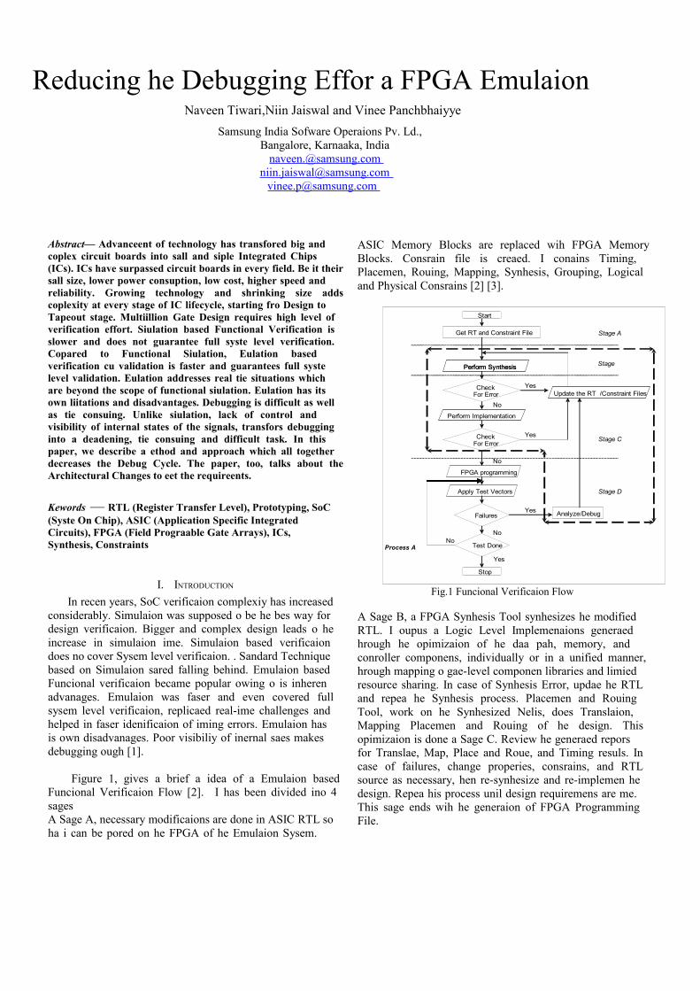
Reducing the Debugging Effort at FPGA EmulationNaveen Tiwari,Nitin Jaiswal and Vineet Panchbhaiyye
Samsung India Software Operations Pvt. Ltd.,Bangalore, Karnataka, India
[email protected]@samsung.com
Abstract— Advancement of technology has transformed big and complex circuit boards into small and simple Integrated Chips (ICs). ICs have surpassed circuit boards in every field. Be it their small size, lower power consumption, low cost, higher speed and reliability. Growing technology and shrinking size adds complexity at every stage of IC lifecycle, starting from Design to Tapeout stage. Multimillion Gate Design requires high level of verification effort. Simulation based Functional Verification is slower and does not guarantee full system level verification. Compared to Functional Simulation, Emulation based verification cum validation is faster and guarantees full system level validation. Emulation addresses real time situations which are beyond the scope of functional simulation. Emulation has its own limitations and disadvantages. Debugging is difficult as well as time consuming. Unlike simulation, lack of control and visibility of internal states of the signals, transforms debugging into a deadening, time consuming and difficult task. In this paper, we describe a method and approach which all together decreases the Debug Cycle. The paper, too, talks about the Architectural Changes to meet the requirements.
Keywords— RTL (Register Transfer Level), Prototyping, SoC (System On Chip), ASIC (Application Specific Integrated Circuits), FPGA (Field Programmable Gate Arrays), ICs, Synthesis, Constraints
I. INTRODUCTION
In recent years, SoC verification complexity has increased considerably. Simulation was supposed to be the best way for design verification. Bigger and complex design leads to the increase in simulation time. Simulation based verification does not cover System level verification. . Standard Technique based on Simulation started falling behind. Emulation based Functional verification became popular owing to its inherent advantages. Emulation was faster and even covered full system level verification, replicated real-time challenges and helped in faster identification of timing errors. Emulation has its own disadvantages. Poor visibility of internal states makes debugging tough [1].
Figure 1, gives a brief a idea of a Emulation based Functional Verification Flow [2]. It has been divided into 4 stages At Stage A, necessary modifications are done in ASIC RTL so that it can be ported on the FPGA of the Emulation System.
ASIC Memory Blocks are replaced with FPGA Memory Blocks. Constraint file is created. It contains Timing, Placement, Routing, Mapping, Synthesis, Grouping, Logical and Physical Constraints [2] [3].
Start
Get RTL and Constraint File
Perform SynthesisPerform Synthesis
CheckFor Error Update the RTL/Constraint Files
Perform Implementation
CheckFor Error
FPGA programming
Apply Test Vectors
Failures
Test Done
Stop
Analyze/Debug
Yes
No
Yes
Yes
Yes
No
NoNo
Stage A
Stage C
Stage D
Stage B
Process A
Fig.1 Functional Verification Flow
At Stage B, a FPGA Synthesis Tool synthesizes the modified RTL. It outputs a Logic Level Implementations generated through the optimization of the data path, memory, and controller components, individually or in a unified manner, through mapping to gate-level component libraries and limited resource sharing. In case of Synthesis Error, update the RTL and repeat the Synthesis process. Placement and Routing Tool, work on the Synthesized Netlist, does Translatiton, Mapping Placement and Routing of the design. This optimization is done at Stage C. Review the generated reports for Translate, Map, Place and Route, and Timing results. In case of failures, change properties, constraints, and RTL source as necessary, then re-synthesize and re-implement the design. Repeat this process until design requirements are met. This stage ends with the generation of FPGA Programming File.
1
A FinFET based robust sense amplifier for
process variations
Vivek Harshey1, A K Saxena
1, S K Manhas
1
Abstract
Process variations inducing transistor characteristics mismatch have emerged
as major challenge to nano-scale circuit design leading to failure of circuits,
such as sense amplifiers. In this paper, we propose a modified current latch
sense amplifier having high tolerance to process variations. The circuit
designed with double gate FINFET technology, utilizes an improved self
compensation technique to overcome variations in transistor characteristics.
The simulations of transistor mismatch (threshold voltage, Vt) using monte-carlo
technique show that, the proposed circuit performs correct circuit functionality
for worst case Vt mismatch of 50mV. This design offers up to 30% higher yield
compared to uncompensated circuit. The design has a minimal penalty for
circuit complexity and speed, and is easily implementable at 45nm/32nm
technology node.
Keywords: FinFET, DRAM, Sense Amplifier, Process Variations, Robustness.
1. Introduction
With the emerging nanoscale devices, SIA (Semiconductor Industry
Association) roadmap identifies FinFET as a candidate for post-planar end-of-
roadmap CMOS device. As the device dimension scales below 100nm, process
variation has emerged as a significant design concern [1, ITRS]. Embedded
memories use sense amplifier for fast sensing. Typically, sense amplifiers use a
pair of matched transistors in a positive feedback environment. A small
difference in voltage level of applied input signals to these matched transistors is
amplified and the resulting logic signals are latched.
Intra die variations due to lithography related critical dimension variations,
fluctuations in dopant density, oxide thickness and parametric variations of
devices causes mismatch in the threshold voltage between the sense transistors
that should ideally be identical structures. If this difference is sufficient to
overcome bit differential voltage developed on the bit-lines of the sense
amplifier then the sense amplifier may latch incorrect signal, and hence the
functionality of the circuit is affected. Since a typical chip may contain hundreds
of thousands of sense amplifiers and if some sense amplifier results in
malfunctioning then it causes loss of yield. This necessitates design of robust
sense amplifiers that have lower failure probability against process variations.
1 Dept. of ECE, IIT Roorkee, Roorkee, Uttarakhand, India-247667;
Design of a Novel CNTFET-Based 1-Bit Full Adder in Deep Submicron Technology
Aminul Islam1, Sachin Pable2, M.W. Akram2, Mohd. Hasan2
Abstract
Process imperfections due to sub-wavelength lithography and device level variations in small-geometry devices such as Random Dopant Fluctuations (RDF) and Line Edge Roughness (LER) cause large variations in their circuit parameters particularly threshold voltage (Vth). Therefore, this paper presents the analyses of various existing 1-bit full adder topologies in light of process, voltage and temperature (PVT) variations to verify their functionality and robustness. This comparison has been carried out in terms of ±3σ process parameters and temperature variations with respect to ± 10% supply voltage (VDD) variation by applying Gaussian distribution and Monte Carlo analysis at 22nm technology node using HSPICE. Transmission gate TG(MOS) topology is found to be the most robust against PVT variations. Hence, a novel Transmission Gate (TG)-Carbon Nano Tube Field Effect Transistor (CNTFET) – based 1-bit full adder called TG(CNT) has also been proposed in this work which is even better than TG(MOS) both in terms of performance and robustness. Keywords (Index): Carbon Nano Tube Field Effect Transistor (CNTFET); Transmission Gate (TG); Random Dopant Fluctuation (RDF); Line Edge Roughness (LER); Energy Delay Product (EDP).
1. Introduction Due to aggressive scaling, random variations in process, voltage and temperature (P, V, T) are posing a major challenge to high performance circuits and system design [1, 2, 3]. The process variations include variation in oxide thickness (∆Tox), channel length (∆L) in short channel devices, channel width (∆W) in narrow channel devices, substrate doping concentration (∆NSUB), channel doping concentration (∆NDEP), critical dimension of polysilicon gate (∆NGATE), source/drain sheet resistance (∆RSH). All these process parameters affect threshold voltage(Vth), which in turn modulates the drain to source current IDS. The Vth variation is normally distributed and its 3σ variation is about 30mV at 180nm technology node [2]. The ubiquitous portable devices demand for low power causing supply voltage scaling thereby making voltage variations a major
1 Dept. of ECE, Birla Institute of Technology (deemed university), Mesra, Ranchi-835215, Jharkhand, India; Email: [email protected].
2 Dept. of Electronics Engg., Aligarh Muslim University, Aligarh, U.P., India.
Design of Robust Subthreshold Circuits
S.D.Pable1, Aminul Islam2, M.W.Akram1, Mohd.Hasan1
Abstract
Subthreshold circuits have emerged as strong alternative for ultra low power applications. At same frequency, subthreshold circuits show orders of magnitude power saving over superthreshold circuits. In subthreshold operating region, leakage current is use as a switching current however, this minute current limits the performance of logic gate. This paper identifies suitable logic family for implementing robust subthreshold circuits. The performance characteristics of different logic families for XOR structure operating in subthreshold region has been compared in 65nm technology. The effect of threshold voltage and temperature variation is also observed for the XOR structure. Dynamic threshold MOS (DTMOS) and Swap body biasing (SBB) are employed to create a robust XOR structure which is much less prone to temperature and threshold voltage variations. Keyword (Index) -Subthreshold, Ultra-low power, Body biasing, Variability, sub-wavelength lithography 1. Introduction Minimizing power consumption is a vital design objective for portable devices. Due to aggressive scaling of transistor size for high performance applications, gate leakage, drain substrate junction band-to-band tunneling current and subthreshold current increases significantly [1]. Considerable work on limiting leakage current has been performed for super threshold circuits [2][3]. The primary motivation for using sub-threshold voltage is to reduce energy. Analysis of energy contours in [4] demonstrated that minimum energy operation occurs in the sub-threshold region. Once the voltage VDD supplied is less than Vth, delay increases exponentially with additional voltage scaling. Moreover, the leakage current integrates over the longer delay. Subthreshold circuits are well suited for certain ultra-low power applications. First, energy-constrained applications such as wireless sensor nodes, RFID tags, hearing aids or implants like pace maker require minimum energy operation. Speed is a secondary consideration for this class of applications, so sub-Vth circuits offer a good solution. Subthreshold circuits can minimize energy for computations executed during the low performance slots. Finally, the parallelism inherent in many signal processing and communication circuits can be exploited to scale voltages into sub-Vth,
1 Dept. of Electronics Engineering, Aligarh Muslim University, Aligarh,U.P.,India; Email: [email protected], [email protected] 2 Dept. of ECE, Birla Institute of Technology (Deemed university), Mesra, Ranchi, Jharkhand, India; Email: [email protected]
CMOS-LTE COMPARATOR AND 2:1 MULTIPLEXER IN FLASH ADC DESIGN
Meghana Kulkarni1, V. Sridhar2 , G.H. Kulkarni3
Abstract This paper proposes 1.8V, 4-bit Flash Analog to Digital converter design using CMOS Linear Tunable Transconductance Element (CMOS-LTE) Comparators and 2:1 multiplexers with 500 nm technology. In this approach the reference voltages are generated by systematically sizing the transistors of CMOS Linear Tunable Transconductance Element thus completely eliminating the resistive ladder network required for the purpose. The circuit of 2:1 multiplexers is implemented to convert thermometer code to binary code. It is observed that with the use CMOS-LTE Comparator Power Supply Rejection (PSR) is improved. The DC simulation result shows the DNL of +0.16/-0.16 LSB and INL of +0.16/-0.104 LSB. Keywords: CMOS-LTE, TIQ, ADC, Mux. 1. Introduction The most important component in the ADC architecture is the comparator. Its role is to convert an input voltage Vin into logic �1� or �0� by comparing the reference voltage Vref with Vin. Some of the comparator structures reported in the literature are differential amplifier latch type, auto zeroed sequentially sampled comparator, dynamic, TIQ (Threshold Inverter Quantizer) comparator and QV (Quantum Voltage) comparator [1-5]. The TIQ comparator has single ended input and is very sensitive to power supply noise [4, 5]. The reference voltages are changed when there is a noise in the power supply voltage. To overcome this problem the CMOS Linear Tunable Transconductance Element (CMOS-LTE) comparator has been proposed, which uses the TIQ comparator concept for the generation of reference voltages. ________________________ 1 Asst. Prof., Dept. of E & C, Gogte Institute of Technology, Belgaum, Karnataka, India; Email:[email protected]. 2 Principal, P.E.S. College of Engineering, Mandya, Karnataka, India; Email:[email protected] . 3 Professor, Dept. of E & E, Gogte Institute of Technology, Belgaum, Karnataka, India; Email:[email protected].
id541234 pdfMachine by Broadgun Software - a great PDF writer! - a great PDF creator! - http://www.pdfmachine.com http://www.broadgun.com


![Creating Polytope Srikanth Devanathan Representations of ......algorithms using polyhedral data structures [14]. Since - trees are prohibitively expensive for higher dimensions, the](https://img.pdfslide.us/doc/110x75/6045e94ea899ae61bc76e841/creating-polytope-srikanth-devanathan-representations-of-algorithms-using.jpg)