Embed Size (px)
Citation preview
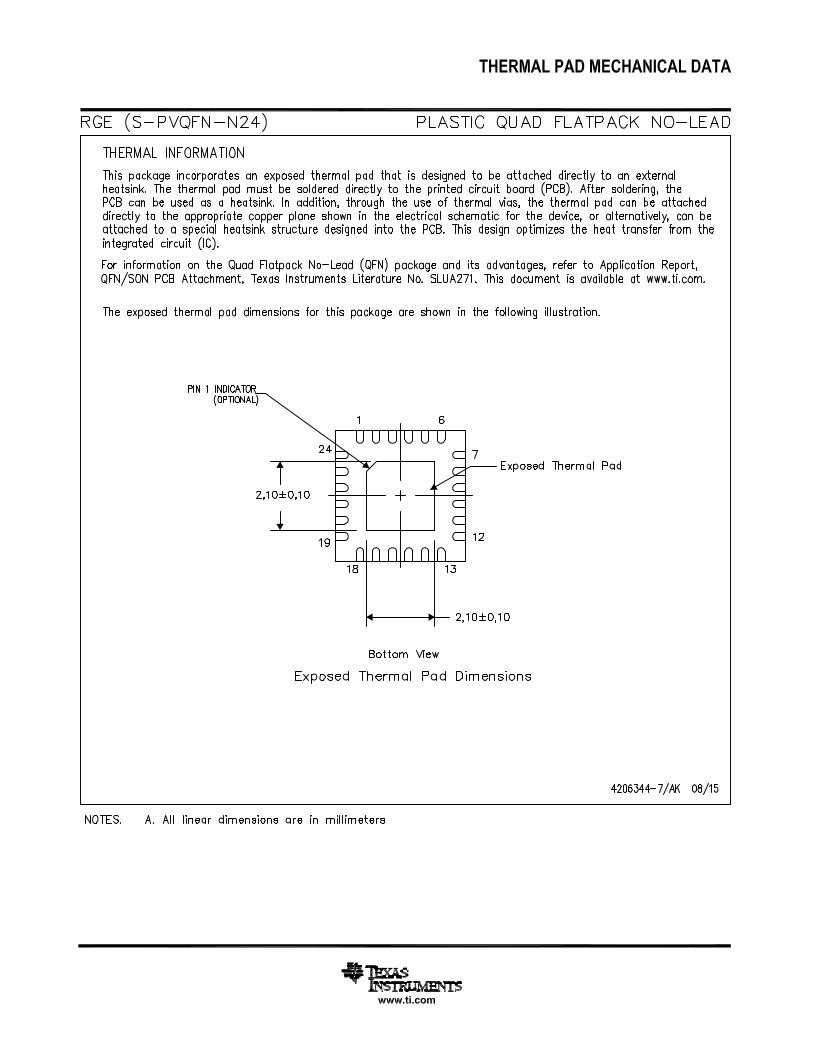
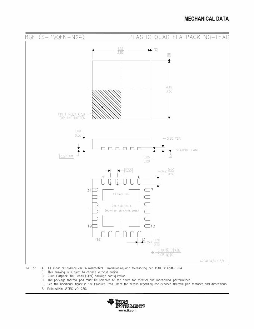
(1) Thermal pad must be connected to VSS.P0025-02
18
17
16
15
14
13
S0
VDD1
Y1
Y1
VDD1
VSS
1
2
3
4
5
6
7 8 9 10 11 12
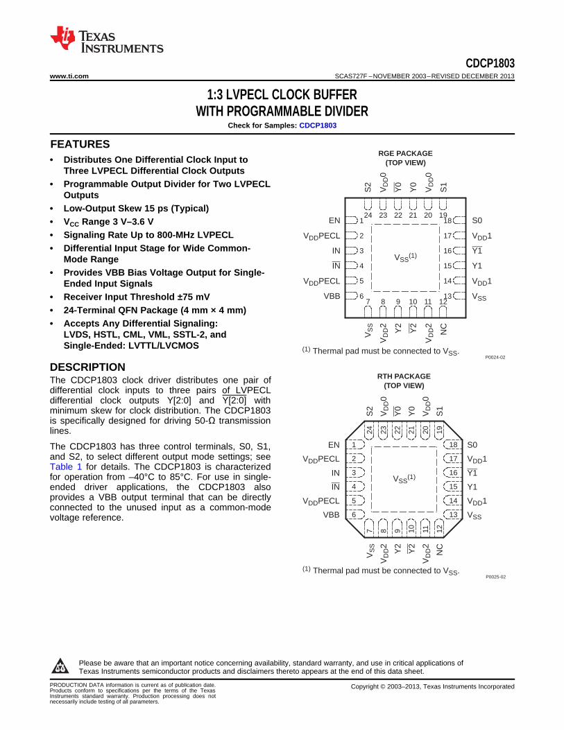
24 23 22 21 20 19EN
VDDPECL
IN
IN
VDDPECL
VBB
S2
VD
D0
Y0
Y0
VD
D0
S1
VS
S
VD
D2
Y2
Y2
VD
D2
NC
VSS(1)
RTH PACKAGE(TOP VIEW)
VSS(1)
S0
VDD1
Y1
Y1
VDD1
VSS
18
17
16
15
14
13
1
2
3
4
5
6
EN
VDDPECL
IN
IN
VDDPECL
VBB
24 23 22 21 20 19
7 8 9 10 11 12
S2
VD
D0
Y0
Y0
VD
D0
S1
VS
S
VD
D2
Y2
Y2
VD
D2
NC
RGE PACKAGE(TOP VIEW)
(1) Thermal pad must be connected to VSS.P0024-02
CDCP1803www.ti.com SCAS727F –NOVEMBER 2003–REVISED DECEMBER 2013
1:3 LVPECL CLOCK BUFFERWITH PROGRAMMABLE DIVIDER
Check for Samples: CDCP1803
1FEATURES• Distributes One Differential Clock Input to
Three LVPECL Differential Clock Outputs• Programmable Output Divider for Two LVPECL
Outputs• Low-Output Skew 15 ps (Typical)• VCC Range 3 V–3.6 V• Signaling Rate Up to 800-MHz LVPECL• Differential Input Stage for Wide Common-
Mode Range• Provides VBB Bias Voltage Output for Single-
Ended Input Signals• Receiver Input Threshold ±75 mV• 24-Terminal QFN Package (4 mm × 4 mm)• Accepts Any Differential Signaling:
LVDS, HSTL, CML, VML, SSTL-2, andSingle-Ended: LVTTL/LVCMOS
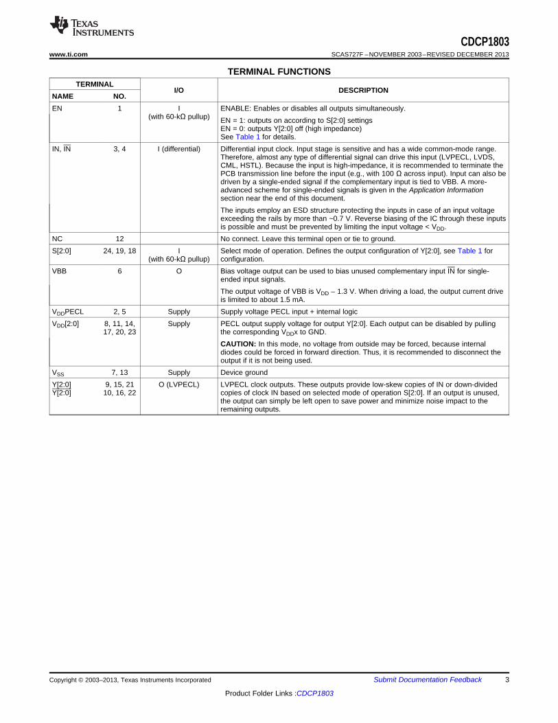
DESCRIPTIONThe CDCP1803 clock driver distributes one pair ofdifferential clock inputs to three pairs of LVPECLdifferential clock outputs Y[2:0] and Y[2:0] withminimum skew for clock distribution. The CDCP1803is specifically designed for driving 50-Ω transmissionlines.
The CDCP1803 has three control terminals, S0, S1,and S2, to select different output mode settings; seeTable 1 for details. The CDCP1803 is characterizedfor operation from –40°C to 85°C. For use in single-ended driver applications, the CDCP1803 alsoprovides a VBB output terminal that can be directlyconnected to the unused input as a common-modevoltage reference.
1
Please be aware that an important notice concerning availability, standard warranty, and use in critical applications ofTexas Instruments semiconductor products and disclaimers thereto appears at the end of this data sheet.
PRODUCTION DATA information is current as of publication date. Copyright © 2003–2013, Texas Instruments IncorporatedProducts conform to specifications per the terms of the TexasInstruments standard warranty. Production processing does notnecessarily include testing of all parameters.
Control
VBB
LVPECL
Y1
Y1
LVPECL
Y2
Y2
LVPECL
Y0
Y0
Div 1Div 2Div 4Div 8Div 16
BiasGeneratorVDD − 1.3 V
(Imax < 1.5 mA)
IN
IN
S2
ENS0
S1
B0059-02
CDCP1803SCAS727F –NOVEMBER 2003–REVISED DECEMBER 2013 www.ti.com
These devices have limited built-in ESD protection. The leads should be shorted together or the device placed in conductive foamduring storage or handling to prevent electrostatic damage to the MOS gates.
FUNCTIONAL BLOCK DIAGRAM
2 Submit Documentation Feedback Copyright © 2003–2013, Texas Instruments Incorporated
Product Folder Links :CDCP1803
CDCP1803www.ti.com SCAS727F –NOVEMBER 2003–REVISED DECEMBER 2013
TERMINAL FUNCTIONSTERMINAL
I/O DESCRIPTIONNAME NO.EN 1 I ENABLE: Enables or disables all outputs simultaneously.
(with 60-kΩ pullup) EN = 1: outputs on according to S[2:0] settingsEN = 0: outputs Y[2:0] off (high impedance)See Table 1 for details.
IN, IN 3, 4 I (differential) Differential input clock. Input stage is sensitive and has a wide common-mode range.Therefore, almost any type of differential signal can drive this input (LVPECL, LVDS,CML, HSTL). Because the input is high-impedance, it is recommended to terminate thePCB transmission line before the input (e.g., with 100 Ω across input). Input can also bedriven by a single-ended signal if the complementary input is tied to VBB. A more-advanced scheme for single-ended signals is given in the Application Informationsection near the end of this document.The inputs employ an ESD structure protecting the inputs in case of an input voltageexceeding the rails by more than ~0.7 V. Reverse biasing of the IC through these inputsis possible and must be prevented by limiting the input voltage < VDD.
NC 12 No connect. Leave this terminal open or tie to ground.S[2:0] 24, 19, 18 I Select mode of operation. Defines the output configuration of Y[2:0], see Table 1 for
(with 60-kΩ pullup) configuration.VBB 6 O Bias voltage output can be used to bias unused complementary input IN for single-
ended input signals.The output voltage of VBB is VDD – 1.3 V. When driving a load, the output current driveis limited to about 1.5 mA.
VDDPECL 2, 5 Supply Supply voltage PECL input + internal logicVDD[2:0] 8, 11, 14, Supply PECL output supply voltage for output Y[2:0]. Each output can be disabled by pulling
17, 20, 23 the corresponding VDDx to GND.CAUTION: In this mode, no voltage from outside may be forced, because internaldiodes could be forced in forward direction. Thus, it is recommended to disconnect theoutput if it is not being used.
VSS 7, 13 Supply Device groundY[2:0] 9, 15, 21 O (LVPECL) LVPECL clock outputs. These outputs provide low-skew copies of IN or down-dividedY[2:0] 10, 16, 22 copies of clock IN based on selected mode of operation S[2:0]. If an output is unused,
the output can simply be left open to save power and minimize noise impact to theremaining outputs.
Copyright © 2003–2013, Texas Instruments Incorporated Submit Documentation Feedback 3
Product Folder Links :CDCP1803
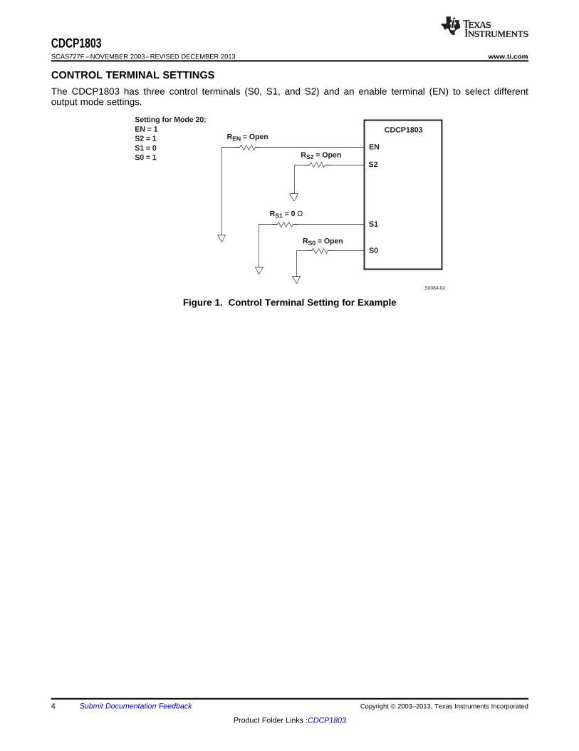
RS0 = Open
EN
CDCP1803
S1
S0
RS1 = 0 Ω
REN = Open
Setting for Mode 20:EN = 1S2 = 1S1 = 0S0 = 1 RS2 = Open
S2
S0084-02
CDCP1803SCAS727F –NOVEMBER 2003–REVISED DECEMBER 2013 www.ti.com
CONTROL TERMINAL SETTINGSThe CDCP1803 has three control terminals (S0, S1, and S2) and an enable terminal (EN) to select differentoutput mode settings.
Figure 1. Control Terminal Setting for Example
4 Submit Documentation Feedback Copyright © 2003–2013, Texas Instruments Incorporated
Product Folder Links :CDCP1803
CDCP1803www.ti.com SCAS727F –NOVEMBER 2003–REVISED DECEMBER 2013
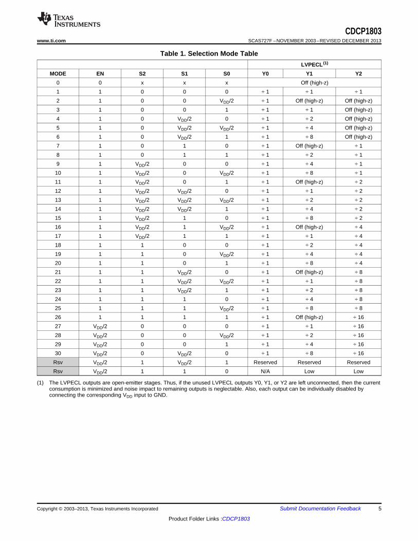
Table 1. Selection Mode TableLVPECL (1)
MODE EN S2 S1 S0 Y0 Y1 Y20 0 x x x Off (high-z)1 1 0 0 0 ÷ 1 ÷ 1 ÷ 12 1 0 0 VDD/2 ÷ 1 Off (high-z) Off (high-z)3 1 0 0 1 ÷ 1 ÷ 1 Off (high-z)4 1 0 VDD/2 0 ÷ 1 ÷ 2 Off (high-z)5 1 0 VDD/2 VDD/2 ÷ 1 ÷ 4 Off (high-z)6 1 0 VDD/2 1 ÷ 1 ÷ 8 Off (high-z)7 1 0 1 0 ÷ 1 Off (high-z) ÷ 18 1 0 1 1 ÷ 1 ÷ 2 ÷ 19 1 VDD/2 0 0 ÷ 1 ÷ 4 ÷ 110 1 VDD/2 0 VDD/2 ÷ 1 ÷ 8 ÷ 111 1 VDD/2 0 1 ÷ 1 Off (high-z) ÷ 212 1 VDD/2 VDD/2 0 ÷ 1 ÷ 1 ÷ 213 1 VDD/2 VDD/2 VDD/2 ÷ 1 ÷ 2 ÷ 214 1 VDD/2 VDD/2 1 ÷ 1 ÷ 4 ÷ 215 1 VDD/2 1 0 ÷ 1 ÷ 8 ÷ 216 1 VDD/2 1 VDD/2 ÷ 1 Off (high-z) ÷ 417 1 VDD/2 1 1 ÷ 1 ÷ 1 ÷ 418 1 1 0 0 ÷ 1 ÷ 2 ÷ 419 1 1 0 VDD/2 ÷ 1 ÷ 4 ÷ 420 1 1 0 1 ÷ 1 ÷ 8 ÷ 421 1 1 VDD/2 0 ÷ 1 Off (high-z) ÷ 822 1 1 VDD/2 VDD/2 ÷ 1 ÷ 1 ÷ 823 1 1 VDD/2 1 ÷ 1 ÷ 2 ÷ 824 1 1 1 0 ÷ 1 ÷ 4 ÷ 825 1 1 1 VDD/2 ÷ 1 ÷ 8 ÷ 826 1 1 1 1 ÷ 1 Off (high-z) ÷ 1627 VDD/2 0 0 0 ÷ 1 ÷ 1 ÷ 1628 VDD/2 0 0 VDD/2 ÷ 1 ÷ 2 ÷ 1629 VDD/2 0 0 1 ÷ 1 ÷ 4 ÷ 1630 VDD/2 0 VDD/2 0 ÷ 1 ÷ 8 ÷ 16
Rsv VDD/2 1 VDD/2 1 Reserved Reserved ReservedRsv VDD/2 1 1 0 N/A Low Low
(1) The LVPECL outputs are open-emitter stages. Thus, if the unused LVPECL outputs Y0, Y1, or Y2 are left unconnected, then the currentconsumption is minimized and noise impact to remaining outputs is neglectable. Also, each output can be individually disabled byconnecting the corresponding VDD input to GND.
Copyright © 2003–2013, Texas Instruments Incorporated Submit Documentation Feedback 5
Product Folder Links :CDCP1803
CDCP1803SCAS727F –NOVEMBER 2003–REVISED DECEMBER 2013 www.ti.com
ABSOLUTE MAXIMUM RATINGSover operating free-air temperature (unless otherwise noted) (1)
VDD Supply voltage –0.3 V to 3.8 VVI Input voltage –0.2 V to (VDD + 0.2 V)VO Output voltage –0.2 V to (VDD + 0.2 V)
Differential short-circuit current, Yn, Yn, IOSD ContinuousElectrostatic discharge (HBM 1.5 kΩ, 100 pF), ESD >2000 VMoisture level 24-terminal QFN package (solder reflow temperature of 235°C) MSL 2
Tstg Storage temperature –65°C to 150°CTJ Maximum junction temperature 125°C
(1) Stresses beyond those listed under absolute maximum ratings may cause permanent damage to the device. These are stress ratingsonly, and functional operation of the device at these or any other conditions beyond those indicated under recommended operatingconditions is not implied. Exposure to absolute-maximum-rated conditions for extended periods may affect device reliability.
RECOMMENDED OPERATING CONDITIONSMIN TYP MAX UNIT
VDD Supply voltage 3 3.3 3.6 VTA Operating free-air temperature –40 85 °C
ELECTRICAL CHARACTERISTICSover operating free-air temperature range (unless otherwise noted)
LVPECL INPUT IN, INPARAMETER TEST CONDITIONS MIN TYP MAX UNIT
fclk Input frequency 0 800 MHzVCM High-level input common mode 1 VDD – 0.3 V
Input voltage swing between IN and IN (1) 500 1300VIN mV
Input voltage swing between IN and IN (2) 125 1300IIN Input current VI = VDD or 0 V ±10 μARIN Input impedance 300 kΩCI Input capacitance at IN, IN 1 pF
(1) Is required to maintain ac specifications(2) Is required to maintain device functionality
6 Submit Documentation Feedback Copyright © 2003–2013, Texas Instruments Incorporated
Product Folder Links :CDCP1803
CDCP1803www.ti.com SCAS727F –NOVEMBER 2003–REVISED DECEMBER 2013
ELECTRICAL CHARACTERISTICS (continued)over operating free-air temperature range (unless otherwise noted)
LVPECL OUTPUT DRIVER Y[2:0], Y[2:0]PARAMETER TEST CONDITIONS MIN TYP MAX UNIT
fclk Output frequency, see Figure 3. 0 800 MHzVOH High-level output voltage Termination with 50 Ω to VDD – 2 V VDD – 1.18 VDD – 0.81 VVOL Low-level output voltage Termination with 50 Ω to VDD – 2 V VDD – 1.98 VDD – 1.55 V
Output voltage swing between Y and Y,VO Termination with 50 Ω to VDD – 2 V 500 mVsee Figure 3.IOZL VDD = 3.6 V, VO = 0 V 5
Output 3-state current μAIOZH VDD = 3.6 V, VO = VDD – 0.8 V 10tr/tf Rise and fall times 20% to 80% of VOUTPP, see Figure 7. 200 350 ps
Output skew between any LVPECLtskpecl(o) See Note A in Figure 6. 15 30 psoutput Y[2:0] and Y[2:0]Crossing point-to-crossing pointtDuty Output duty-cycle distortion (1) –50 50 psdistortion
tsk(pp) Part-to-part skew Any Y, see Note B in Figure 6. 50 300 psCO Output capacitance VO = VDD or GND 1 pFLOAD Expected output load 50 Ω
(1) For an 800-MHz signal, the 50-ps error would result in a duty cycle distortion of ±4% when driven by an ideal clock input signal.
LVPECL INPUT-TO-LVPECL OUTPUT PARAMETERSPARAMETER TEST CONDITIONS MIN TYP MAX UNIT
tpd(lh) Propagation delay, rising edge VOX to VOX 320 600 pstpd(hl) Propagation delay, falling edge VOX to VOX 320 600 pstsk(p) LVPECL pulse skew VOX to VOX, see Note C in Figure 6. 100 ps
JITTER CHARACTERISTICSPARAMETER TEST CONDITIONS MIN TYP MAX UNIT
JITTER CHARACTERISTICS12 kHz to 20 MHz,fout = 250 MHz to 800 MHz, 0.15divide-by-1 modeAdditive phase jitter from input totjitterLVPECL ps rmsLVPECL output Y[2:0], see Figure 2. 50 kHz to 40 MHz,fout = 250 MHz to 800 MHz, 0.25divide-by-1 mode
Copyright © 2003–2013, Texas Instruments Incorporated Submit Documentation Feedback 7
Product Folder Links :CDCP1803
−160
−155
−150
−145
−140
−135
−130
−125
−120
−115
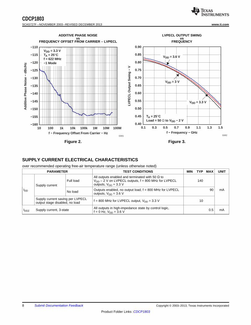
−110VDD = 3.3 VTA = 25°Cf = 622 MHz÷1 Mode
Add
itive
Pha
se N
oise
− d
Bc/
Hz
f − Frequency Offset From Carrier − Hz
10 100 1k 100M10k 100k 10M1M
G001
f − Frequency − GHz
0.40
0.45
0.50
0.55
0.60
0.65
0.70
0.75
0.80
0.85
0.90
0.1 0.3 0.5 0.7 0.9 1.1 1.3 1.5LV
PE
CL
Out
put S
win
g −
V
TA = 25°CLoad = 50 Ω to VDD − 2 V
VDD = 3.6 V
VDD = 3.3 V
VDD = 3 V
G002
CDCP1803SCAS727F –NOVEMBER 2003–REVISED DECEMBER 2013 www.ti.com
ADDITIVE PHASE NOISE LVPECL OUTPUT SWINGvs vs
FREQUENCY OFFSET FROM CARRIER – LVPECL FREQUENCY
Figure 2. Figure 3.
SUPPLY CURRENT ELECTRICAL CHARACTERISTICSover recommended operating free-air temperature range (unless otherwise noted)
PARAMETER TEST CONDITIONS MIN TYP MAX UNITAll outputs enabled and terminated with 50 Ω to
Full load VDD – 2 V on LVPECL outputs, f = 800 MHz for LVPECL 140outputs, VDD = 3.3 VSupply current
IDD Outputs enabled, no output load, f = 800 MHz for LVPECL 90 mANo load outputs, VDD = 3.6 VSupply current saving per LVPECL f = 800 MHz for LVPECL output, VDD = 3.3 V 10output stage disabled, no load
All outputs in high-impedance state by control logic,IDDZ Supply current, 3-state 0.5 mAf = 0 Hz, VDD = 3.6 V
8 Submit Documentation Feedback Copyright © 2003–2013, Texas Instruments Incorporated
Product Folder Links :CDCP1803
130
135
140
145
150
100 300 500 700 900 1100 1300 1500
f − Frequency − MHz
I DD
− S
uppl
y C
urre
nt −
mA
3 LVPECL Outputs 1) Running
VDD = 3.3 V,TA = 25C,50 to VDD −2 V for L VPECL
G003
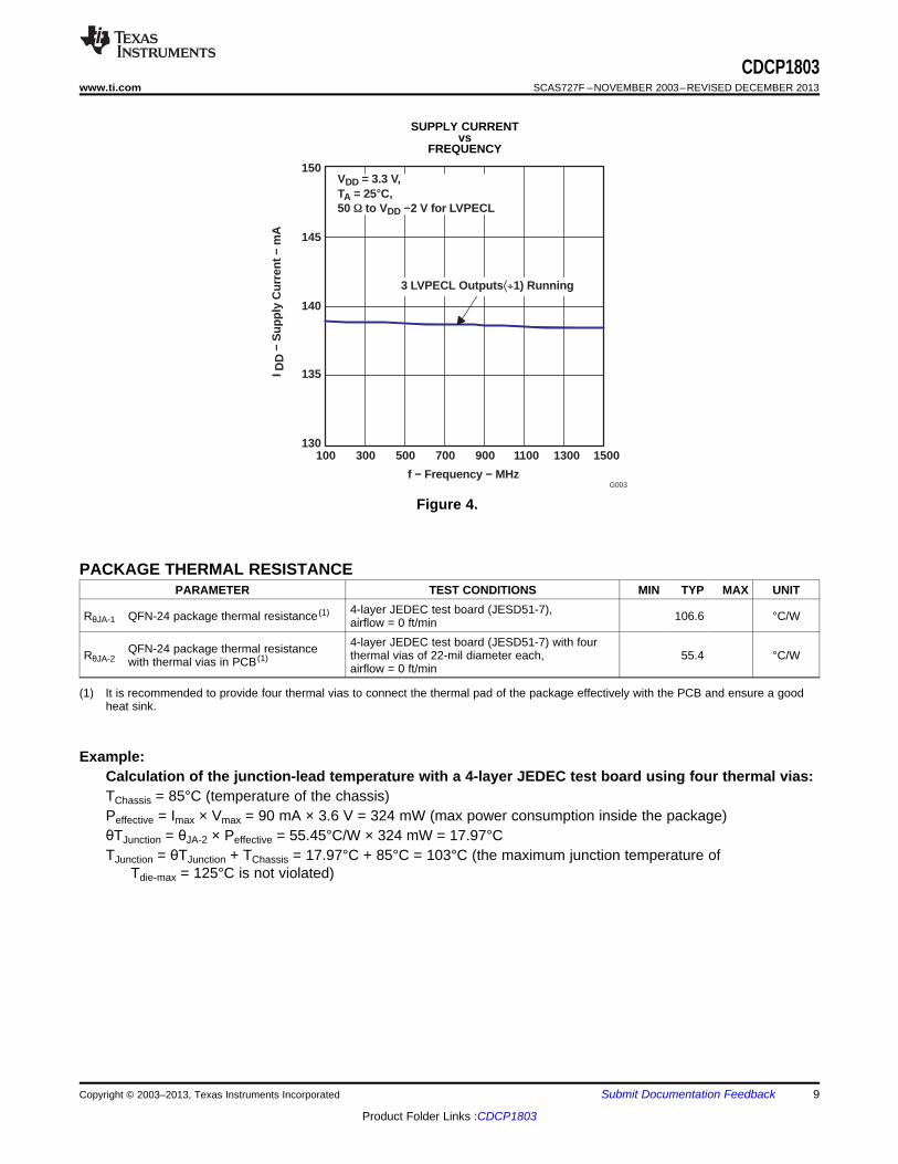
CDCP1803www.ti.com SCAS727F –NOVEMBER 2003–REVISED DECEMBER 2013
SUPPLY CURRENTvs
FREQUENCY
Figure 4.
PACKAGE THERMAL RESISTANCEPARAMETER TEST CONDITIONS MIN TYP MAX UNIT
4-layer JEDEC test board (JESD51-7),RθJA-1 QFN-24 package thermal resistance (1) 106.6 °C/Wairflow = 0 ft/min4-layer JEDEC test board (JESD51-7) with fourQFN-24 package thermal resistanceRθJA-2 thermal vias of 22-mil diameter each, 55.4 °C/Wwith thermal vias in PCB (1)airflow = 0 ft/min
(1) It is recommended to provide four thermal vias to connect the thermal pad of the package effectively with the PCB and ensure a goodheat sink.
Example:Calculation of the junction-lead temperature with a 4-layer JEDEC test board using four thermal vias:TChassis = 85°C (temperature of the chassis)Peffective = Imax × Vmax = 90 mA × 3.6 V = 324 mW (max power consumption inside the package)θTJunction = θJA-2 × Peffective = 55.45°C/W × 324 mW = 17.97°CTJunction = θTJunction + TChassis = 17.97°C + 85°C = 103°C (the maximum junction temperature of
Tdie-max = 125°C is not violated)
Copyright © 2003–2013, Texas Instruments Incorporated Submit Documentation Feedback 9
Product Folder Links :CDCP1803
I − Load − mA
0.0
0.5
1.0
1.5
2.0
2.5
3.0
3.5
4.0
−5 0 5 10 15 20 25 30 35
VDD = 3.3 V
VB
B −
Out
put R
efer
ence
Vol
tage
− V
G004
CDCP1803SCAS727F –NOVEMBER 2003–REVISED DECEMBER 2013 www.ti.com
CONTROL INPUT CHARACTERISTICSover recommended operating free-air temperature range
PARAMETER TEST CONDITIONS MIN TYP MAX UNITtsu Setup time, S0, S1, S2, and EN terminals before clock IN 25 nsth Hold time, S0, S1, S2, and EN terminals after clock IN 0 ns
Time between latching the EN low transition and when allt(disable) outputs are disabled (how much time is required until the 10 ns
outputs turn off)Time between latching the EN low-to-high transition and when
t(enable) outputs are enabled based on control settings (how much time 1 μspasses before the outputs carry valid signals)
Rpullup Internal pullup resistor on S[2:0] and EN input 42 60 78 kΩVIH(H) Three-level input high, S0, S1, S2, and EN terminals (1) 0.9 VDD VVIL(L) Three-level low, S0, S1, S2, and EN terminals 0.1 VDD VIIH VI = VDD –5 μA
Input current, S0, S1, S2, and EN terminalsIIL VI = GND 38 85 μA
(1) Leaving this terminal floating automatically pulls the logic level high to VDD through an internal pullup resistor of 60 kΩ.
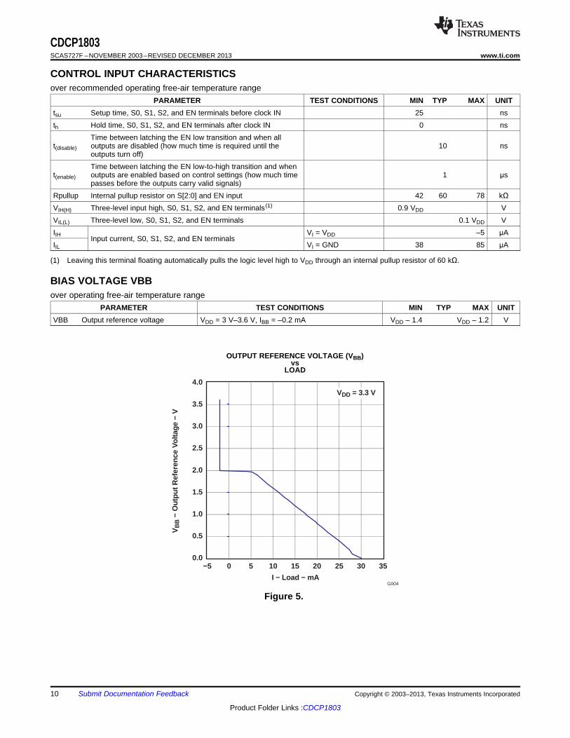
BIAS VOLTAGE VBBover operating free-air temperature range
PARAMETER TEST CONDITIONS MIN TYP MAX UNITVBB Output reference voltage VDD = 3 V–3.6 V, IBB = –0.2 mA VDD – 1.4 VDD – 1.2 V
OUTPUT REFERENCE VOLTAGE (VBB)vs
LOAD
Figure 5.
10 Submit Documentation Feedback Copyright © 2003–2013, Texas Instruments Incorporated
Product Folder Links :CDCP1803
|YnYn|
Yn
Yn
VOH
VOL
80%
20%
0 V
tr tf
VOUT(pp)
T0058-02
IN
IN
Y0
Y0
tpd(LH1)
Y1
Y1
tpd(LH2)
Y2
Y2
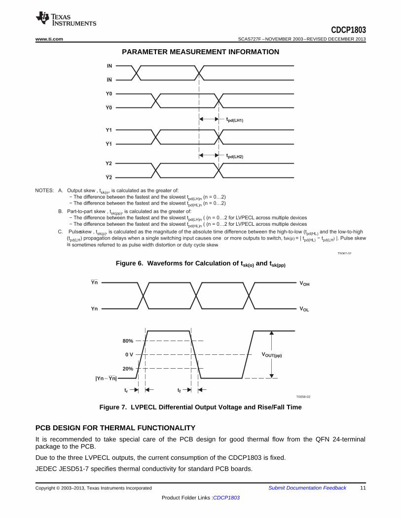
NOTES: A. Output skew , t , is calculated as the greater of:sk(o)
− The difference between the fastest and the slowest t (n = 0…2)pd(LH)n
− The difference between the fastest and the slowest t (n = 0…2)pd(HL)n
B. Part-to-part skew , t , is calculated as the greater of:sk(pp)
− The difference between the fastest and the slowest t ( (n = 0…2 for LVPECL across multiple devicespd(LH)n
− The difference between the fastest and the slowest t ( (n = 0…2 for LVPECL across multiple devicespd(HL)n
C. Pulseskew , t , is calculated as the magnitude of the absolute time difference between the high-to-low (t and the low-to-highsk(p) pd(HL)
(tpd(LH pd(HL) pd(LH) propagation delays when a single switching input causes one or more outputs to switch, t = | t − t |. Pulse skewsk(p) )
is sometimes referred to as pulse width distortion or duty cycle skew.
T0067-02
CDCP1803www.ti.com SCAS727F –NOVEMBER 2003–REVISED DECEMBER 2013
PARAMETER MEASUREMENT INFORMATION
Figure 6. Waveforms for Calculation of tsk(o) and tsk(pp)
Figure 7. LVPECL Differential Output Voltage and Rise/Fall Time
PCB DESIGN FOR THERMAL FUNCTIONALITYIt is recommended to take special care of the PCB design for good thermal flow from the QFN 24-terminalpackage to the PCB.
Due to the three LVPECL outputs, the current consumption of the CDCP1803 is fixed.
JEDEC JESD51-7 specifies thermal conductivity for standard PCB boards.
Copyright © 2003–2013, Texas Instruments Incorporated Submit Documentation Feedback 11
Product Folder Links :CDCP1803
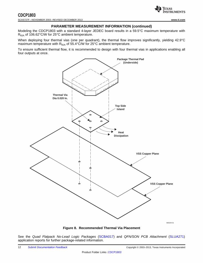
Package Thermal Pad(Underside)
Top SideIsland
Thermal ViaDia 0.020 In.
HeatDissipation
VSS Copper Plane
VSS Copper Plane
M0029-01
CDCP1803SCAS727F –NOVEMBER 2003–REVISED DECEMBER 2013 www.ti.com
PARAMETER MEASUREMENT INFORMATION (continued)Modeling the CDCP1803 with a standard 4-layer JEDEC board results in a 59.5°C maximum temperature withRθJA of 106.62°C/W for 25°C ambient temperature.
When deploying four thermal vias (one per quadrant), the thermal flow improves significantly, yielding 42.9°Cmaximum temperature with RθJA of 55.4°C/W for 25°C ambient temperature.
To ensure sufficient thermal flow, it is recommended to design with four thermal vias in applications enabling allfour outputs at once.
Figure 8. Recommended Thermal Via Placement
See the Quad Flatpack No-Lead Logic Packages (SCBA017) and QFN/SON PCB Attachment (SLUA271)application reports for further package-related information.
12 Submit Documentation Feedback Copyright © 2003–2013, Texas Instruments Incorporated
Product Folder Links :CDCP1803
LVPECL
130 Ω
83 Ω
CDCP1803
50 Ω
50 Ω
130 Ω
83 Ω
S0086-02
IN
IN
IN
150 Ω
150 Ω
CAC
CAC
50 Ω
50 Ω
IN
CDCP1803
C
VBB
50 Ω
50 Ω
S0085-02
LVPECL
CDCP1803www.ti.com SCAS727F –NOVEMBER 2003–REVISED DECEMBER 2013
APPLICATION INFORMATION
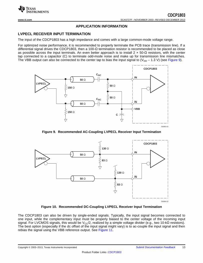
LVPECL RECEIVER INPUT TERMINATIONThe input of the CDCP1803 has a high impedance and comes with a large common-mode voltage range.
For optimized noise performance, it is recommended to properly terminate the PCB trace (transmission line). If adifferential signal drives the CDCP1803, then a 100-Ω termination resistor is recommended to be placed as closeas possible across the input terminals. An even better approach is to install 2 × 50-Ω resistors, with the centertap connected to a capacitor (C) to terminate odd-mode noise and make up for transmission line mismatches.The VBB output can also be connected to the center tap to bias the input signal to (VDD – 1.3 V) (see Figure 9).
Figure 9. Recommended AC-Coupling LVPECL Receiver Input Termination
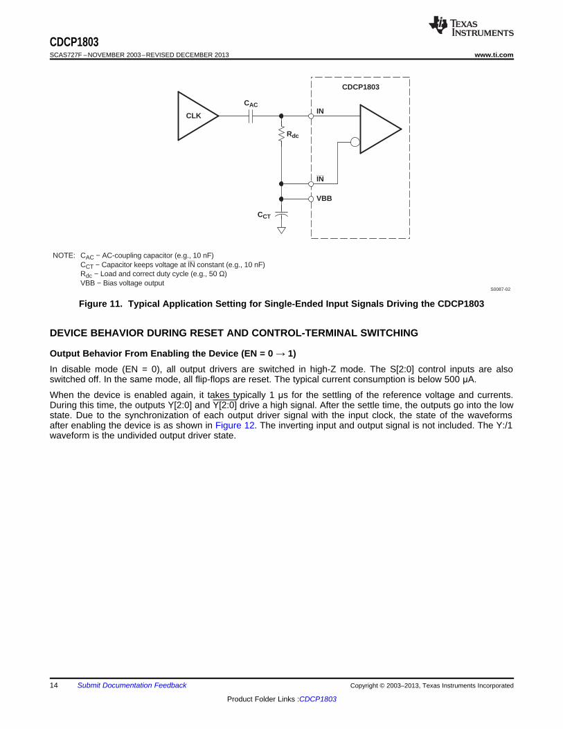
Figure 10. Recommended DC-Coupling LVPECL Receiver Input Termination
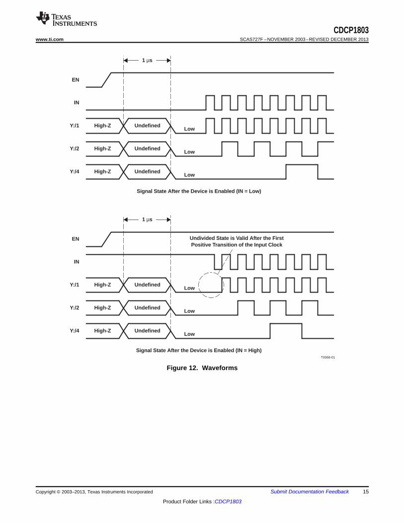
The CDCP1803 can also be driven by single-ended signals. Typically, the input signal becomes connected toone input, while the complementary input must be properly biased to the center voltage of the incoming inputsignal. For LVCMOS signals, this would be VCC/2, realized by a simple voltage divider (e.g., two 10-kΩ resistors).The best option (especially if the dc offset of the input signal might vary) is to ac-couple the input signal and thenrebias the signal using the VBB reference output. See Figure 11.
Copyright © 2003–2013, Texas Instruments Incorporated Submit Documentation Feedback 13
Product Folder Links :CDCP1803
INCLK
CAC
IN
CDCP1803
CCT
VBB
Rdc
NOTE: CAC − AC-coupling capacitor (e.g., 10 nF)CCT − Capacitor keeps voltage at IN constant (e.g., 10 nF)Rdc − Load and correct duty cycle (e.g., 50 Ω)VBB − Bias voltage output
S0087-02
CDCP1803SCAS727F –NOVEMBER 2003–REVISED DECEMBER 2013 www.ti.com
Figure 11. Typical Application Setting for Single-Ended Input Signals Driving the CDCP1803
DEVICE BEHAVIOR DURING RESET AND CONTROL-TERMINAL SWITCHING
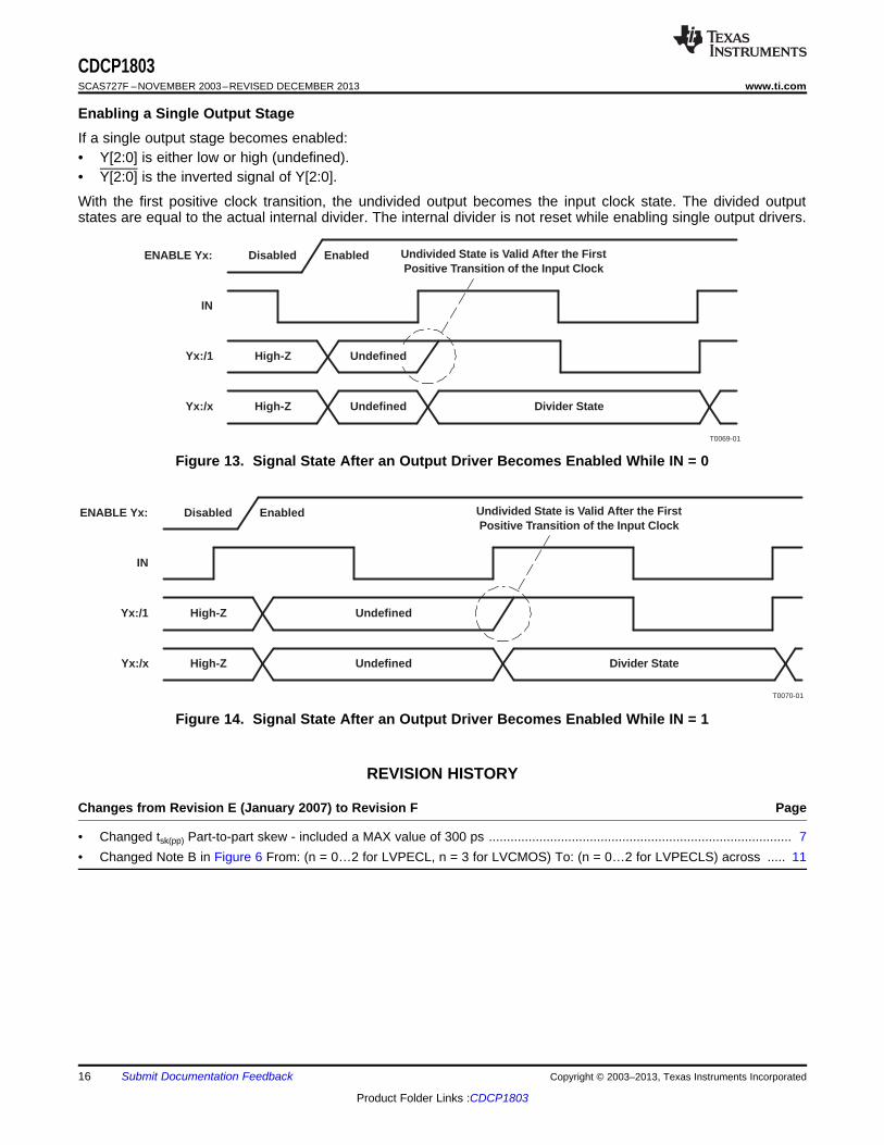
Output Behavior From Enabling the Device (EN = 0 → 1)In disable mode (EN = 0), all output drivers are switched in high-Z mode. The S[2:0] control inputs are alsoswitched off. In the same mode, all flip-flops are reset. The typical current consumption is below 500 μA.
When the device is enabled again, it takes typically 1 μs for the settling of the reference voltage and currents.During this time, the outputs Y[2:0] and Y[2:0] drive a high signal. After the settle time, the outputs go into the lowstate. Due to the synchronization of each output driver signal with the input clock, the state of the waveformsafter enabling the device is as shown in Figure 12. The inverting input and output signal is not included. The Y:/1waveform is the undivided output driver state.
14 Submit Documentation Feedback Copyright © 2003–2013, Texas Instruments Incorporated
Product Folder Links :CDCP1803
High-Z
EN
IN
Y:/1 UndefinedLow
High-ZY:/2 UndefinedLow
High-ZY:/4 UndefinedLow
1 µs
Signal State After the Device is Enabled (IN = Low)
High-Z
EN
IN
Y:/1 UndefinedLow
High-ZY:/2 UndefinedLow
High-ZY:/4 UndefinedLow
1 µs
Signal State After the Device is Enabled (IN = High)
Undivided State is V alid After the FirstPositive T ransition of the Input Clock
T0068-01
CDCP1803www.ti.com SCAS727F –NOVEMBER 2003–REVISED DECEMBER 2013
Figure 12. Waveforms
Copyright © 2003–2013, Texas Instruments Incorporated Submit Documentation Feedback 15
Product Folder Links :CDCP1803
High-Z
ENABLE Yx:
IN
Yx:/1 Undefined
High-ZYx:/x Undefined Divider State
EnabledDisabled Undivided State is V alid After the FirstPositive T ransition of the Input Clock
T0070-01
High-Z
ENABLE Yx:
IN
Yx:/1
High-ZYx:/x Undefined
EnabledDisabled
Divider State
Undivided State is V alid After the FirstPositive T ransition of the Input Clock
Undefined
T0069-01
CDCP1803SCAS727F –NOVEMBER 2003–REVISED DECEMBER 2013 www.ti.com
Enabling a Single Output StageIf a single output stage becomes enabled:• Y[2:0] is either low or high (undefined).• Y[2:0] is the inverted signal of Y[2:0].
With the first positive clock transition, the undivided output becomes the input clock state. The divided outputstates are equal to the actual internal divider. The internal divider is not reset while enabling single output drivers.
Figure 13. Signal State After an Output Driver Becomes Enabled While IN = 0
Figure 14. Signal State After an Output Driver Becomes Enabled While IN = 1
spacerREVISION HISTORY
Changes from Revision E (January 2007) to Revision F Page
• Changed tsk(pp) Part-to-part skew - included a MAX value of 300 ps .................................................................................... 7• Changed Note B in Figure 6 From: (n = 0…2 for LVPECL, n = 3 for LVCMOS) To: (n = 0…2 for LVPECLS) across ..... 11
16 Submit Documentation Feedback Copyright © 2003–2013, Texas Instruments Incorporated
Product Folder Links :CDCP1803
PACKAGE OPTION ADDENDUM
www.ti.com 15-Apr-2017
Addendum-Page 1
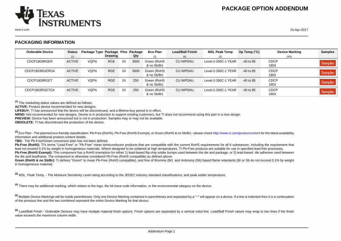
PACKAGING INFORMATION
Orderable Device Status(1)
Package Type PackageDrawing
Pins PackageQty
Eco Plan(2)
Lead/Ball Finish(6)
MSL Peak Temp(3)
Op Temp (°C) Device Marking(4/5)
Samples
CDCP1803RGER ACTIVE VQFN RGE 24 3000 Green (RoHS& no Sb/Br)
CU NIPDAU Level-2-260C-1 YEAR -40 to 85 CDCP1803
CDCP1803RGERG4 ACTIVE VQFN RGE 24 3000 Green (RoHS& no Sb/Br)
CU NIPDAU Level-2-260C-1 YEAR -40 to 85 CDCP1803
CDCP1803RGET ACTIVE VQFN RGE 24 250 Green (RoHS& no Sb/Br)
CU NIPDAU Level-2-260C-1 YEAR -40 to 85 CDCP1803
CDCP1803RGETG4 ACTIVE VQFN RGE 24 250 Green (RoHS& no Sb/Br)
CU NIPDAU Level-2-260C-1 YEAR -40 to 85 CDCP1803
(1) The marketing status values are defined as follows:ACTIVE: Product device recommended for new designs.LIFEBUY: TI has announced that the device will be discontinued, and a lifetime-buy period is in effect.NRND: Not recommended for new designs. Device is in production to support existing customers, but TI does not recommend using this part in a new design.PREVIEW: Device has been announced but is not in production. Samples may or may not be available.OBSOLETE: TI has discontinued the production of the device.
(2) Eco Plan - The planned eco-friendly classification: Pb-Free (RoHS), Pb-Free (RoHS Exempt), or Green (RoHS & no Sb/Br) - please check http://www.ti.com/productcontent for the latest availabilityinformation and additional product content details.TBD: The Pb-Free/Green conversion plan has not been defined.Pb-Free (RoHS): TI's terms "Lead-Free" or "Pb-Free" mean semiconductor products that are compatible with the current RoHS requirements for all 6 substances, including the requirement thatlead not exceed 0.1% by weight in homogeneous materials. Where designed to be soldered at high temperatures, TI Pb-Free products are suitable for use in specified lead-free processes.Pb-Free (RoHS Exempt): This component has a RoHS exemption for either 1) lead-based flip-chip solder bumps used between the die and package, or 2) lead-based die adhesive used betweenthe die and leadframe. The component is otherwise considered Pb-Free (RoHS compatible) as defined above.Green (RoHS & no Sb/Br): TI defines "Green" to mean Pb-Free (RoHS compatible), and free of Bromine (Br) and Antimony (Sb) based flame retardants (Br or Sb do not exceed 0.1% by weightin homogeneous material)
(3) MSL, Peak Temp. - The Moisture Sensitivity Level rating according to the JEDEC industry standard classifications, and peak solder temperature.
(4) There may be additional marking, which relates to the logo, the lot trace code information, or the environmental category on the device.
(5) Multiple Device Markings will be inside parentheses. Only one Device Marking contained in parentheses and separated by a "~" will appear on a device. If a line is indented then it is a continuationof the previous line and the two combined represent the entire Device Marking for that device.
(6) Lead/Ball Finish - Orderable Devices may have multiple material finish options. Finish options are separated by a vertical ruled line. Lead/Ball Finish values may wrap to two lines if the finishvalue exceeds the maximum column width.
PACKAGE OPTION ADDENDUM
www.ti.com 15-Apr-2017
Addendum-Page 2
Important Information and Disclaimer:The information provided on this page represents TI's knowledge and belief as of the date that it is provided. TI bases its knowledge and belief on informationprovided by third parties, and makes no representation or warranty as to the accuracy of such information. Efforts are underway to better integrate information from third parties. TI has taken andcontinues to take reasonable steps to provide representative and accurate information but may not have conducted destructive testing or chemical analysis on incoming materials and chemicals.TI and TI suppliers consider certain information to be proprietary, and thus CAS numbers and other limited information may not be available for release.
In no event shall TI's liability arising out of such information exceed the total purchase price of the TI part(s) at issue in this document sold by TI to Customer on an annual basis.
OTHER QUALIFIED VERSIONS OF CDCP1803 :
• Enhanced Product: CDCP1803-EP
NOTE: Qualified Version Definitions:
• Enhanced Product - Supports Defense, Aerospace and Medical Applications
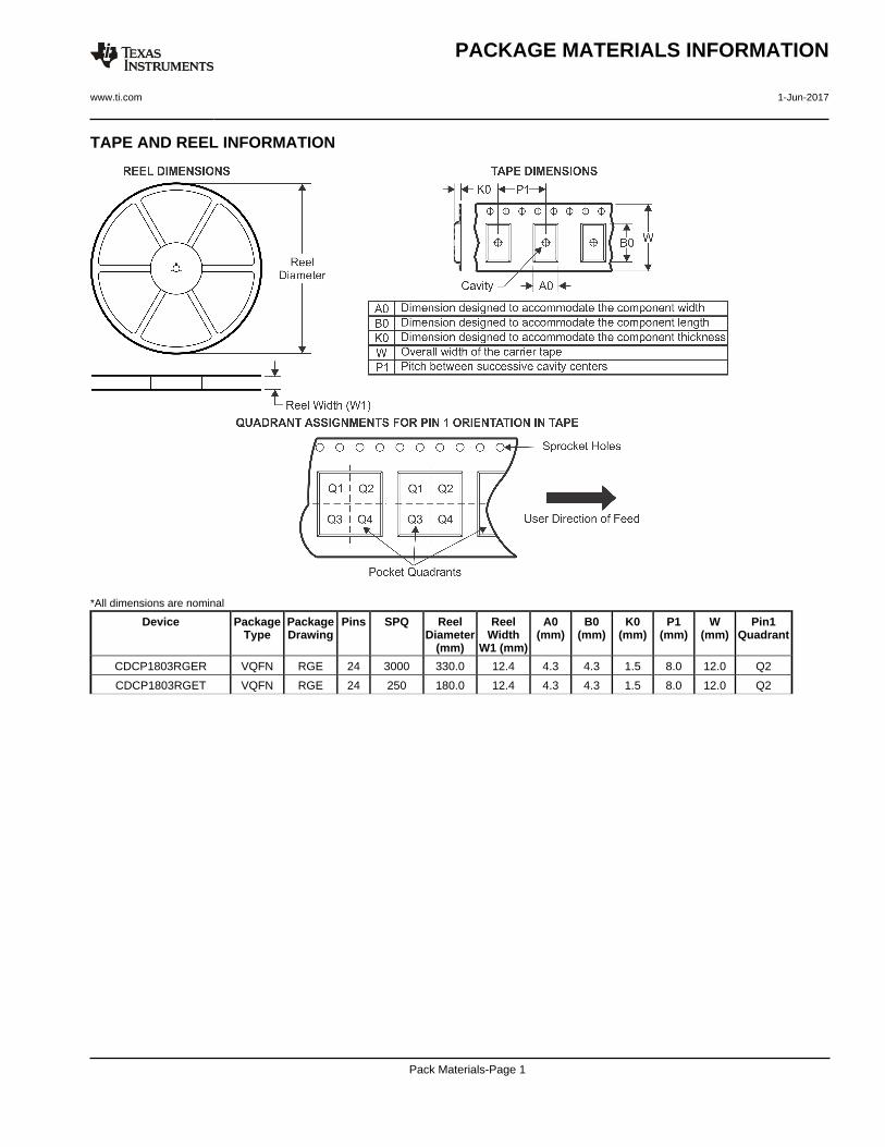
TAPE AND REEL INFORMATION
*All dimensions are nominal
Device PackageType
PackageDrawing
Pins SPQ ReelDiameter
(mm)
ReelWidth
W1 (mm)
A0(mm)
B0(mm)
K0(mm)
P1(mm)
W(mm)
Pin1Quadrant
CDCP1803RGER VQFN RGE 24 3000 330.0 12.4 4.3 4.3 1.5 8.0 12.0 Q2
CDCP1803RGET VQFN RGE 24 250 180.0 12.4 4.3 4.3 1.5 8.0 12.0 Q2
PACKAGE MATERIALS INFORMATION
www.ti.com 1-Jun-2017
Pack Materials-Page 1
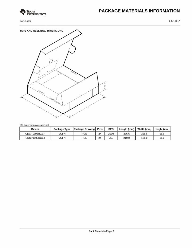
*All dimensions are nominal
Device Package Type Package Drawing Pins SPQ Length (mm) Width (mm) Height (mm)
CDCP1803RGER VQFN RGE 24 3000 336.6 336.6 28.6
CDCP1803RGET VQFN RGE 24 250 210.0 185.0 35.0
PACKAGE MATERIALS INFORMATION
www.ti.com 1-Jun-2017
Pack Materials-Page 2
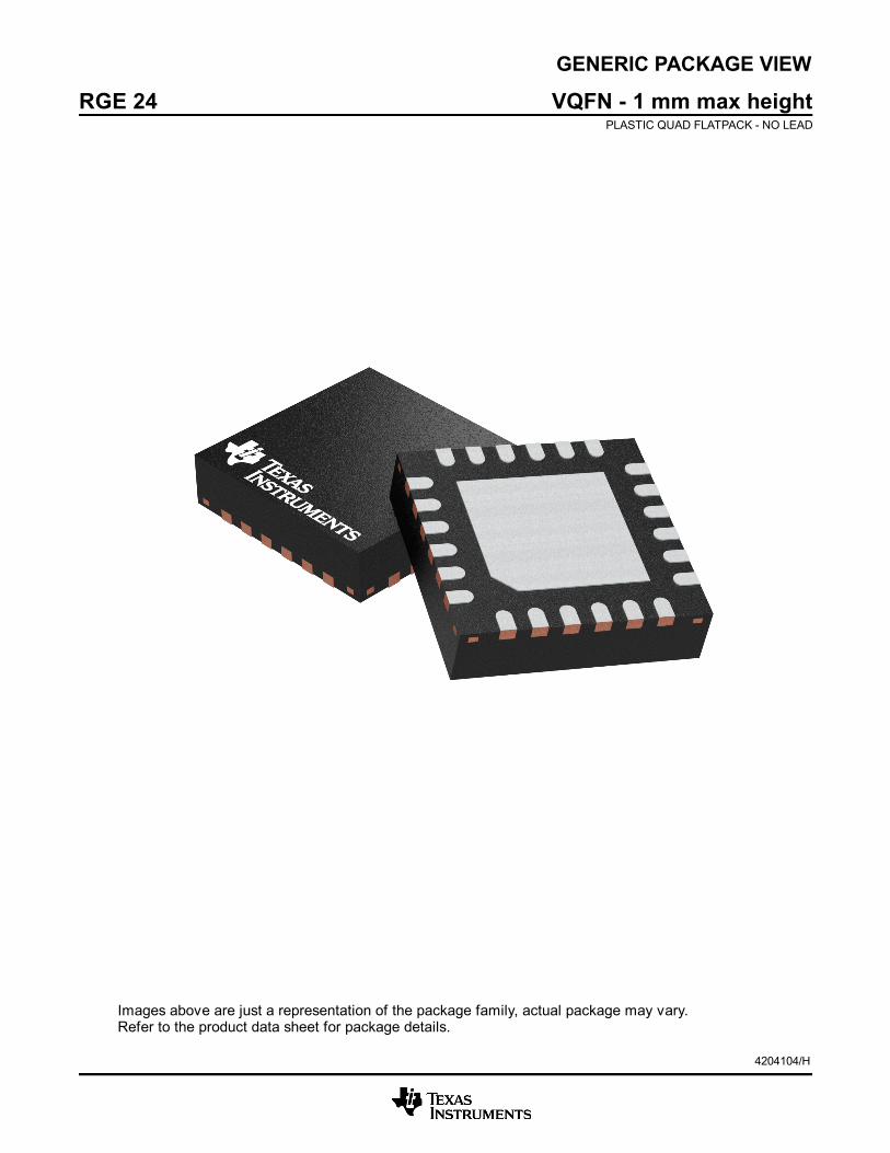
GENERIC PACKAGE VIEW
Images above are just a representation of the package family, actual package may vary.Refer to the product data sheet for package details.
RGE 24 VQFN - 1 mm max heightPLASTIC QUAD FLATPACK - NO LEAD
4204104/H
IMPORTANT NOTICE
Texas Instruments Incorporated (TI) reserves the right to make corrections, enhancements, improvements and other changes to itssemiconductor products and services per JESD46, latest issue, and to discontinue any product or service per JESD48, latest issue. Buyersshould obtain the latest relevant information before placing orders and should verify that such information is current and complete.TI’s published terms of sale for semiconductor products (http://www.ti.com/sc/docs/stdterms.htm) apply to the sale of packaged integratedcircuit products that TI has qualified and released to market. Additional terms may apply to the use or sale of other types of TI products andservices.Reproduction of significant portions of TI information in TI data sheets is permissible only if reproduction is without alteration and isaccompanied by all associated warranties, conditions, limitations, and notices. TI is not responsible or liable for such reproduceddocumentation. Information of third parties may be subject to additional restrictions. Resale of TI products or services with statementsdifferent from or beyond the parameters stated by TI for that product or service voids all express and any implied warranties for theassociated TI product or service and is an unfair and deceptive business practice. TI is not responsible or liable for any such statements.Buyers and others who are developing systems that incorporate TI products (collectively, “Designers”) understand and agree that Designersremain responsible for using their independent analysis, evaluation and judgment in designing their applications and that Designers havefull and exclusive responsibility to assure the safety of Designers' applications and compliance of their applications (and of all TI productsused in or for Designers’ applications) with all applicable regulations, laws and other applicable requirements. Designer represents that, withrespect to their applications, Designer has all the necessary expertise to create and implement safeguards that (1) anticipate dangerousconsequences of failures, (2) monitor failures and their consequences, and (3) lessen the likelihood of failures that might cause harm andtake appropriate actions. Designer agrees that prior to using or distributing any applications that include TI products, Designer willthoroughly test such applications and the functionality of such TI products as used in such applications.TI’s provision of technical, application or other design advice, quality characterization, reliability data or other services or information,including, but not limited to, reference designs and materials relating to evaluation modules, (collectively, “TI Resources”) are intended toassist designers who are developing applications that incorporate TI products; by downloading, accessing or using TI Resources in anyway, Designer (individually or, if Designer is acting on behalf of a company, Designer’s company) agrees to use any particular TI Resourcesolely for this purpose and subject to the terms of this Notice.TI’s provision of TI Resources does not expand or otherwise alter TI’s applicable published warranties or warranty disclaimers for TIproducts, and no additional obligations or liabilities arise from TI providing such TI Resources. TI reserves the right to make corrections,enhancements, improvements and other changes to its TI Resources. TI has not conducted any testing other than that specificallydescribed in the published documentation for a particular TI Resource.Designer is authorized to use, copy and modify any individual TI Resource only in connection with the development of applications thatinclude the TI product(s) identified in such TI Resource. NO OTHER LICENSE, EXPRESS OR IMPLIED, BY ESTOPPEL OR OTHERWISETO ANY OTHER TI INTELLECTUAL PROPERTY RIGHT, AND NO LICENSE TO ANY TECHNOLOGY OR INTELLECTUAL PROPERTYRIGHT OF TI OR ANY THIRD PARTY IS GRANTED HEREIN, including but not limited to any patent right, copyright, mask work right, orother intellectual property right relating to any combination, machine, or process in which TI products or services are used. Informationregarding or referencing third-party products or services does not constitute a license to use such products or services, or a warranty orendorsement thereof. Use of TI Resources may require a license from a third party under the patents or other intellectual property of thethird party, or a license from TI under the patents or other intellectual property of TI.TI RESOURCES ARE PROVIDED “AS IS” AND WITH ALL FAULTS. TI DISCLAIMS ALL OTHER WARRANTIES ORREPRESENTATIONS, EXPRESS OR IMPLIED, REGARDING RESOURCES OR USE THEREOF, INCLUDING BUT NOT LIMITED TOACCURACY OR COMPLETENESS, TITLE, ANY EPIDEMIC FAILURE WARRANTY AND ANY IMPLIED WARRANTIES OFMERCHANTABILITY, FITNESS FOR A PARTICULAR PURPOSE, AND NON-INFRINGEMENT OF ANY THIRD PARTY INTELLECTUALPROPERTY RIGHTS. TI SHALL NOT BE LIABLE FOR AND SHALL NOT DEFEND OR INDEMNIFY DESIGNER AGAINST ANY CLAIM,INCLUDING BUT NOT LIMITED TO ANY INFRINGEMENT CLAIM THAT RELATES TO OR IS BASED ON ANY COMBINATION OFPRODUCTS EVEN IF DESCRIBED IN TI RESOURCES OR OTHERWISE. IN NO EVENT SHALL TI BE LIABLE FOR ANY ACTUAL,DIRECT, SPECIAL, COLLATERAL, INDIRECT, PUNITIVE, INCIDENTAL, CONSEQUENTIAL OR EXEMPLARY DAMAGES INCONNECTION WITH OR ARISING OUT OF TI RESOURCES OR USE THEREOF, AND REGARDLESS OF WHETHER TI HAS BEENADVISED OF THE POSSIBILITY OF SUCH DAMAGES.Unless TI has explicitly designated an individual product as meeting the requirements of a particular industry standard (e.g., ISO/TS 16949and ISO 26262), TI is not responsible for any failure to meet such industry standard requirements.Where TI specifically promotes products as facilitating functional safety or as compliant with industry functional safety standards, suchproducts are intended to help enable customers to design and create their own applications that meet applicable functional safety standardsand requirements. Using products in an application does not by itself establish any safety features in the application. Designers mustensure compliance with safety-related requirements and standards applicable to their applications. Designer may not use any TI products inlife-critical medical equipment unless authorized officers of the parties have executed a special contract specifically governing such use.Life-critical medical equipment is medical equipment where failure of such equipment would cause serious bodily injury or death (e.g., lifesupport, pacemakers, defibrillators, heart pumps, neurostimulators, and implantables). Such equipment includes, without limitation, allmedical devices identified by the U.S. Food and Drug Administration as Class III devices and equivalent classifications outside the U.S.TI may expressly designate certain products as completing a particular qualification (e.g., Q100, Military Grade, or Enhanced Product).Designers agree that it has the necessary expertise to select the product with the appropriate qualification designation for their applicationsand that proper product selection is at Designers’ own risk. Designers are solely responsible for compliance with all legal and regulatoryrequirements in connection with such selection.Designer will fully indemnify TI and its representatives against any damages, costs, losses, and/or liabilities arising out of Designer’s non-compliance with the terms and provisions of this Notice.
Mailing Address: Texas Instruments, Post Office Box 655303, Dallas, Texas 75265Copyright © 2018, Texas Instruments Incorporated