Embed Size (px)
Citation preview
www.ti.com
FEATURES
APPLICATIONS
RELATED PRODUCTS
DESCRIPTION
ADS5440-EPSGLS359–AUGUST 2006
13-BIT 210-MSPS ANALOG-TO-DIGITAL CONVERTER
• TQFP-80 PowerPAD™ Package• Controlled Baseline • Pin Compatible With the ADS5444
– One Assembly • Military Temperature Range = –55°C to 125°C– One Test Site (1) Component qualification in accordance with JEDEC and
industry standards to ensure reliable operation over an– One Fabrication Site extended temperature range. This includes, but is not limitedto, Highly Accelerated Stress Test (HAST) or biased 85/85,• Extended Temperature Performance of –55°Ctemperature cycle, autoclave or unbiased HAST,to 125°Celectromigration, bond intermetallic life, and mold compoundlife. Such qualification testing should not be viewed as• Enhanced Diminishing Manufacturingjustifying use of this component beyond specifiedSources (DMS) Supportperformance and environmental limits.
• Enhanced Product-Change Notification• Qualification Pedigree(1)
• Test and Measurement• 13-Bit Resolution• Software-Defined Radio• 210-MSPS Sample Rate• Multichannel Base Station Receivers• SNR = 69 dBc at 100-MHz IF and 210 MSPS• Base Station Tx Digital Predistortion• SFDR = 76 dBc at 100-MHz IF and 210 MSPS• Communications Instrumentation• SNR = 68.1 dBc at 230-MHz IF and 210 MSPS
• SFDR = 74 dBc at 230-MHz IF and 210 MSPS• 2.2-VPP Differential Input Voltage • ADS5424 - 14-Bit, 105-MSPS ADC• Fully Buffered Analog Inputs • ADS5423 - 14-Bit, 80-MSPS ADC• 5-V Analog Supply Voltage • ADS5444 - 13-Bit, 250-MSPS ADC• LVDS Compatible Outputs• Total Power Dissipation: 2 W• Offset Binary Output Format
The ADS5440 is a 13-bit 210-MSPS analog-to-digital converter (ADC) that operates from a 5-V supply, whileproviding LVDS-compatible digital outputs from a 3.3-V supply. The ADS5440 input buffer isolates the internalswitching of the onboard track and hold (T&H) from disturbing the signal source. An internal reference generatoris also provided to further simplify the system design. The ADS5440 has outstanding low noise and linearity overinput frequency.
Please be aware that an important notice concerning availability, standard warranty, and use in critical applications of TexasInstruments semiconductor products and disclaimers thereto appears at the end of this data sheet.
PowerPAD is a trademark of Texas Instruments.
PRODUCTION DATA information is current as of publication date. Copyright © 2006, Texas Instruments IncorporatedProducts conform to specifications per the terms of the TexasInstruments standard warranty. Production processing does notnecessarily include testing of all parameters.
www.ti.com
Reference
TimingCLK
OVR D[12:0]
CLK
5
DRY
VREF
AINAIN
TH1
5 5
Σ
DAC2ADC2
ADC3Σ
DAC1ADC1
AVDD DVDD
GND
Digital Error Correction
+
−
+
−
B0061-01
DRYOVR
A1 TH2 A2 A3TH3
ADS5440-EPSGLS359–AUGUST 2006
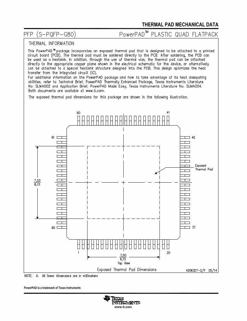
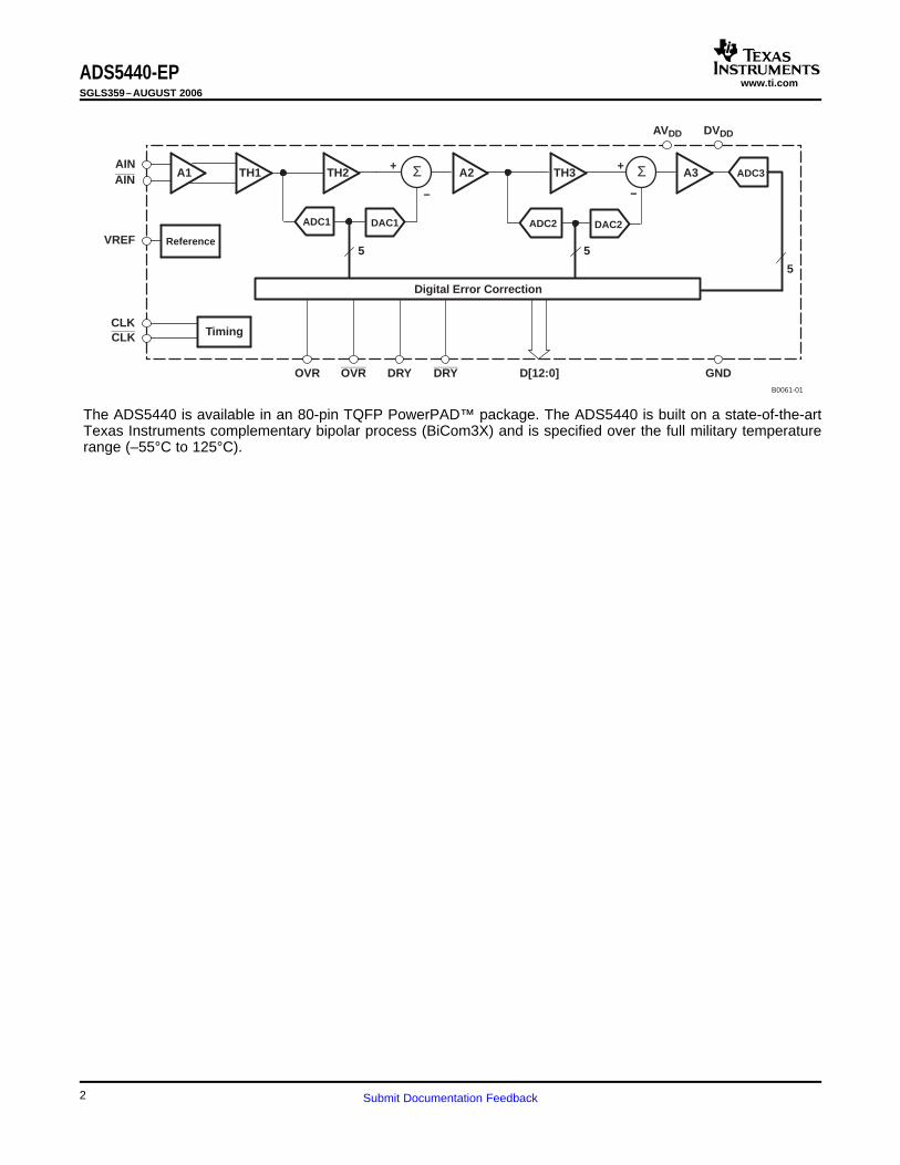
The ADS5440 is available in an 80-pin TQFP PowerPAD™ package. The ADS5440 is built on a state-of-the-artTexas Instruments complementary bipolar process (BiCom3X) and is specified over the full military temperaturerange (–55°C to 125°C).
2 Submit Documentation Feedback
www.ti.com
ABSOLUTE MAXIMUM RATINGS
0.1
1
10
100
1000
120 130 140 150 160 170 180
Wirebond V oiding Fail Mode
Electromigration Fail Mode
Continuous TJ − C
Yea
rs E
stim
ated
Life
ADS5440-EPSGLS359–AUGUST 2006
This integrated circuit can be damaged by ESD. Texas Instruments recommends that all integrated circuits be handled withappropriate precautions. Failure to observe proper handling and installation procedures can cause damage.
ESD damage can range from subtle performance degradation to complete device failure. Precision integrated circuits may bemore susceptible to damage because very small parametric changes could cause the device not to meet its publishedspecifications.
PACKAGING/ORDERING INFORMATION (1)
Product Package Package Specified Package Ordering TransportLead Designator (1) Temperature Marking Number Media,
Range Quantity
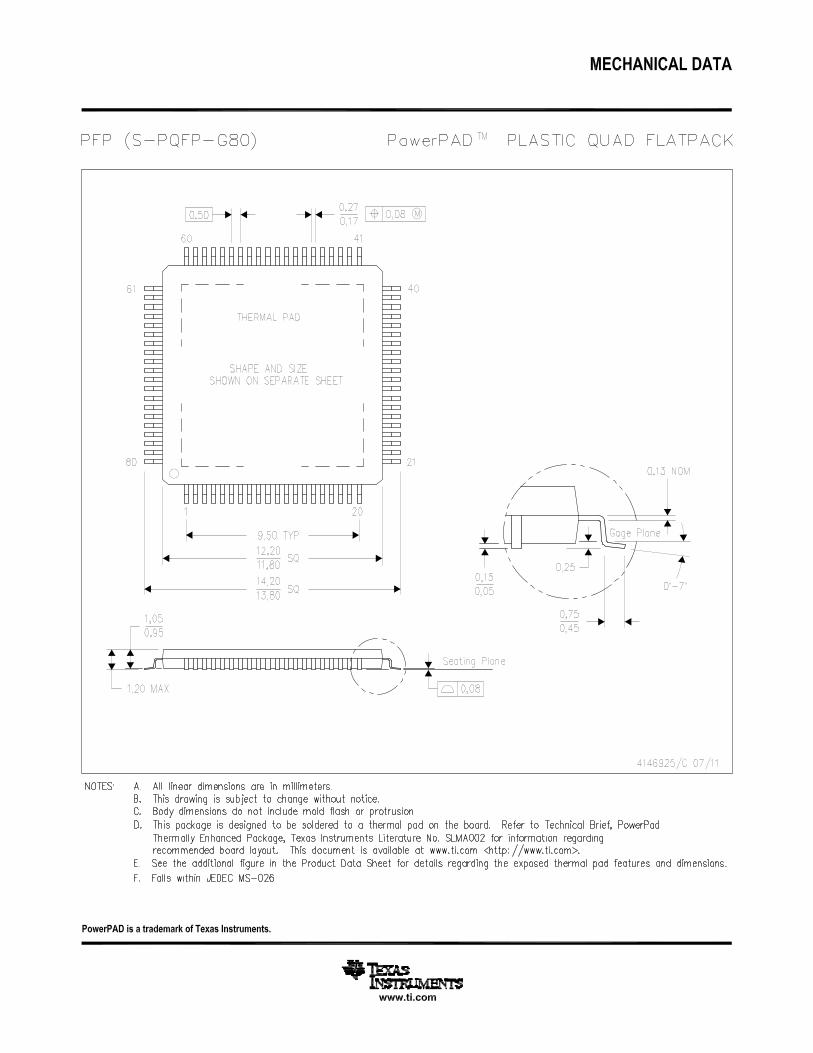
HTQFP-80 (2) ADS5440MPFPEP Tray, 96ADS5440 PFP –55°C to 125°C ADS5440M-EPPowerPAD
(1) For the most current product and ordering information, see the Package Option Addendum located at the end of this data sheet.(2) Thermal pad size: 7,5 mm x 7,5 mm (typ)
over operating free-air temperature range (unless otherwise noted) (1)
VALUE/UNIT
AVDD to GND 6 VSupply voltage
DRVDD to GND 5 V
Analog input to GND –0.3 V to AVDD + 0.3 V
Clock input to GND –0.3 V to AVDD + 0.3 V
CLK to CLK ±2.5 V
Digital data output to GND –0.3 V to DRVDD + 0.3 V
Operating temperature range –55°C to 125°C
Maximum junction temperature 150°C
Storage temperature range –65°C to 150°C
ESD Human Body Model (HBM) 2.5 kV
(1) Stresses above these ratings may cause permanent damage. Exposure to absolute maximum conditions for extended periods maydegrade device reliability. These are stress ratings only and functional operation of the device at these or any other conditions beyondthose specified is not implied.
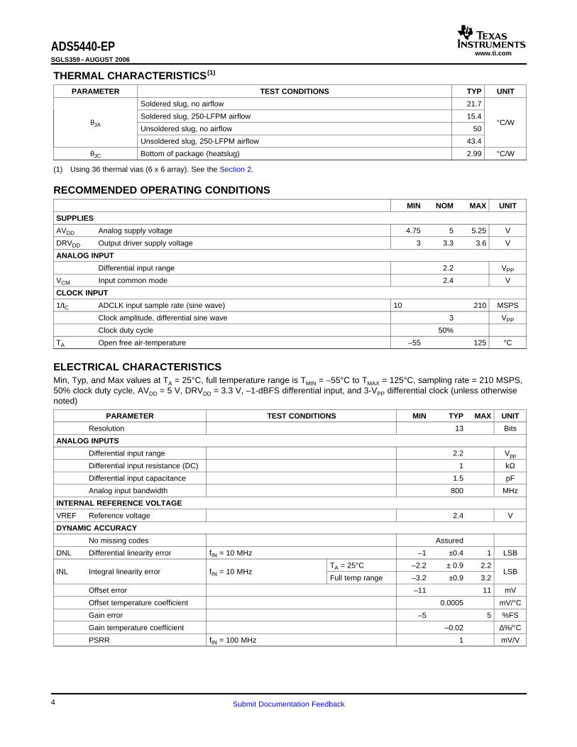
Figure 1. ADS5440MPFPEP Operating Life Derating Chart
3Submit Documentation Feedback
www.ti.com
THERMAL CHARACTERISTICS (1)
RECOMMENDED OPERATING CONDITIONS
ELECTRICAL CHARACTERISTICS
ADS5440-EPSGLS359–AUGUST 2006
PARAMETER TEST CONDITIONS TYP UNIT
Soldered slug, no airflow 21.7
Soldered slug, 250-LFPM airflow 15.4θJA °C/W
Unsoldered slug, no airflow 50
Unsoldered slug, 250-LFPM airflow 43.4
θJC Bottom of package (heatslug) 2.99 °C/W
(1) Using 36 thermal vias (6 x 6 array). See the Section 2.
MIN NOM MAX UNIT
SUPPLIES
AVDD Analog supply voltage 4.75 5 5.25 V
DRVDD Output driver supply voltage 3 3.3 3.6 V
ANALOG INPUT
Differential input range 2.2 VPP
VCM Input common mode 2.4 V
CLOCK INPUT
1/tC ADCLK input sample rate (sine wave) 10 210 MSPS
Clock amplitude, differential sine wave 3 VPP
Clock duty cycle 50%
TA Open free air-temperature –55 125 °C
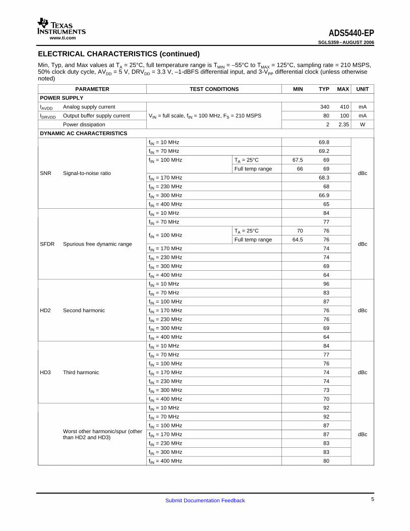
Min, Typ, and Max values at TA = 25°C, full temperature range is TMIN = –55°C to TMAX = 125°C, sampling rate = 210 MSPS,50% clock duty cycle, AVDD = 5 V, DRVDD = 3.3 V, –1-dBFS differential input, and 3-VPP differential clock (unless otherwisenoted)
PARAMETER TEST CONDITIONS MIN TYP MAX UNIT
Resolution 13 Bits
ANALOG INPUTS
Differential input range 2.2 Vpp
Differential input resistance (DC) 1 kΩ
Differential input capacitance 1.5 pF
Analog input bandwidth 800 MHz
INTERNAL REFERENCE VOLTAGE
VREF Reference voltage 2.4 V
DYNAMIC ACCURACY
No missing codes Assured
DNL Differential linearity error fIN = 10 MHz –1 ±0.4 1 LSB
TA = 25°C –2.2 ± 0.9 2.2INL Integral linearity error fIN = 10 MHz LSB
Full temp range –3.2 ±0.9 3.2
Offset error –11 11 mV
Offset temperature coefficient 0.0005 mV/°C
Gain error –5 5 %FS
Gain temperature coefficient –0.02 ∆%/°C
PSRR fIN = 100 MHz 1 mV/V
4 Submit Documentation Feedback
www.ti.comADS5440-EP
SGLS359–AUGUST 2006
ELECTRICAL CHARACTERISTICS (continued)Min, Typ, and Max values at TA = 25°C, full temperature range is TMIN = –55°C to TMAX = 125°C, sampling rate = 210 MSPS,50% clock duty cycle, AVDD = 5 V, DRVDD = 3.3 V, –1-dBFS differential input, and 3-VPP differential clock (unless otherwisenoted)
PARAMETER TEST CONDITIONS MIN TYP MAX UNIT
POWER SUPPLY
IAVDD Analog supply current 340 410 mA
IDRVDD Output buffer supply current VIN = full scale, fIN = 100 MHz, FS = 210 MSPS 80 100 mA
Power dissipation 2 2.35 W
DYNAMIC AC CHARACTERISTICS
fIN = 10 MHz 69.8
fIN = 70 MHz 69.2
fIN = 100 MHz TA = 25°C 67.5 69
Full temp range 66 69SNR Signal-to-noise ratio dBc
fIN = 170 MHz 68.3
fIN = 230 MHz 68
fIN = 300 MHz 66.9
fIN = 400 MHz 65
fIN = 10 MHz 84
fIN = 70 MHz 77
TA = 25°C 70 76fIN = 100 MHz
Full temp range 64.5 76SFDR Spurious free dynamic range dBc
fIN = 170 MHz 74
fIN = 230 MHz 74
fIN = 300 MHz 69
fIN = 400 MHz 64
fIN = 10 MHz 96
fIN = 70 MHz 83
fIN = 100 MHz 87
HD2 Second harmonic fIN = 170 MHz 76 dBc
fIN = 230 MHz 76
fIN = 300 MHz 69
fIN = 400 MHz 64
fIN = 10 MHz 84
fIN = 70 MHz 77
fIN = 100 MHz 76
HD3 Third harmonic fIN = 170 MHz 74 dBc
fIN = 230 MHz 74
fIN = 300 MHz 73
fIN = 400 MHz 70
fIN = 10 MHz 92
fIN = 70 MHz 92
fIN = 100 MHz 87Worst other harmonic/spur (other fIN = 170 MHz 87 dBcthan HD2 and HD3)
fIN = 230 MHz 83
fIN = 300 MHz 83
fIN = 400 MHz 80
5Submit Documentation Feedback
www.ti.comADS5440-EPSGLS359–AUGUST 2006
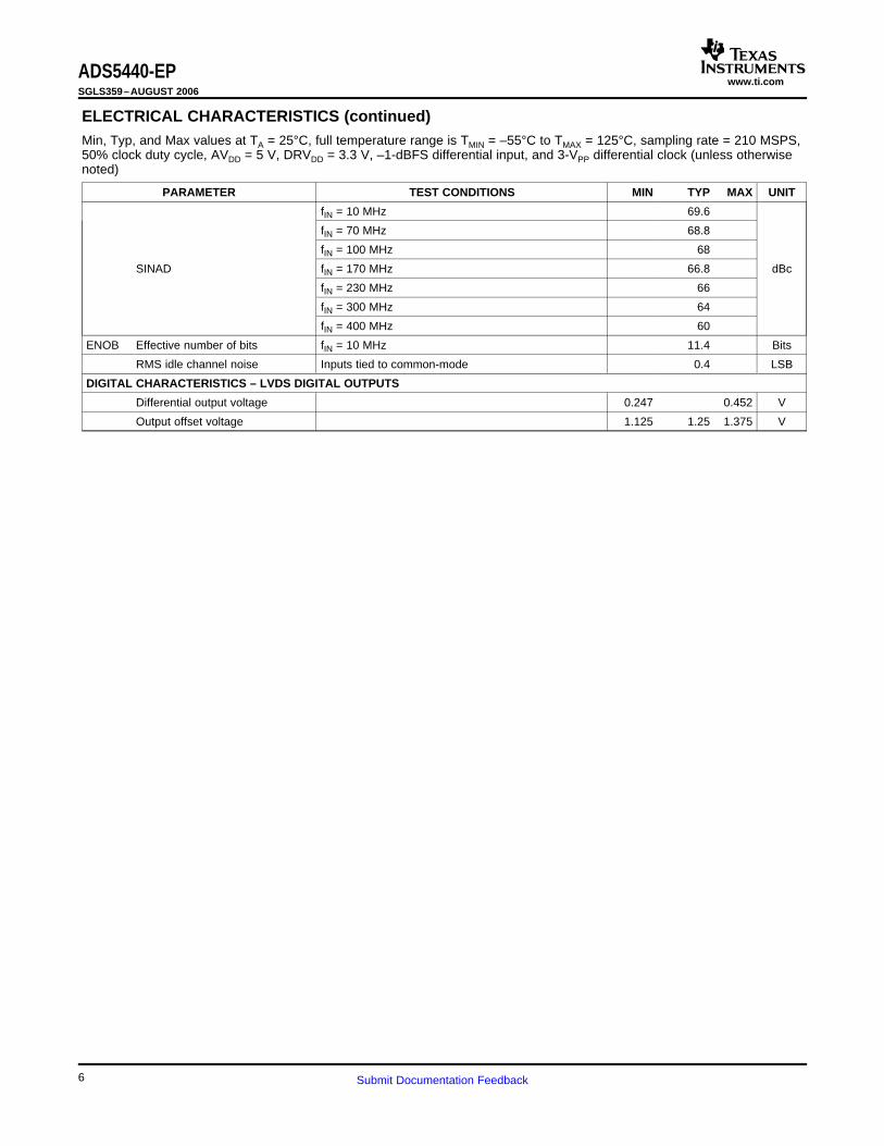
ELECTRICAL CHARACTERISTICS (continued)Min, Typ, and Max values at TA = 25°C, full temperature range is TMIN = –55°C to TMAX = 125°C, sampling rate = 210 MSPS,50% clock duty cycle, AVDD = 5 V, DRVDD = 3.3 V, –1-dBFS differential input, and 3-VPP differential clock (unless otherwisenoted)
PARAMETER TEST CONDITIONS MIN TYP MAX UNIT
fIN = 10 MHz 69.6
fIN = 70 MHz 68.8
fIN = 100 MHz 68
SINAD fIN = 170 MHz 66.8 dBc
fIN = 230 MHz 66
fIN = 300 MHz 64
fIN = 400 MHz 60
ENOB Effective number of bits fIN = 10 MHz 11.4 Bits
RMS idle channel noise Inputs tied to common-mode 0.4 LSB
DIGITAL CHARACTERISTICS – LVDS DIGITAL OUTPUTS
Differential output voltage 0.247 0.452 V
Output offset voltage 1.125 1.25 1.375 V
6 Submit Documentation Feedback
www.ti.com
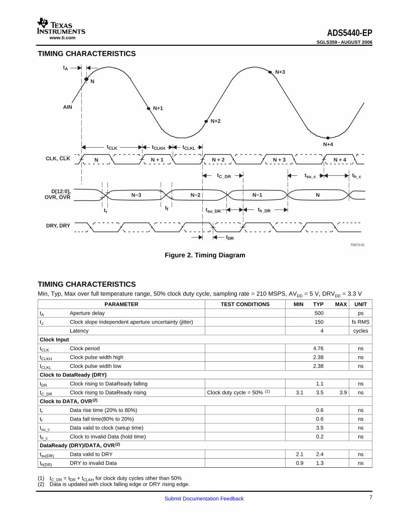
TIMING CHARACTERISTICS
N
N+1
N+2
N+3
N+4
NN−1N−2N−3
tA
tsu_c th_c
th_DR
N + 1N N + 2 N + 3 N + 4
tC_DR
tCLK tCLKL
CLK, CLK
D[12:0],OVR, OVR
DRY, DRY
AIN
tCLKH
tDR
tsu_DR
T0073-01
trtf
TIMING CHARACTERISTICS
ADS5440-EPSGLS359–AUGUST 2006
Figure 2. Timing Diagram
Min, Typ, Max over full temperature range, 50% clock duty cycle, sampling rate = 210 MSPS, AVDD = 5 V, DRVDD = 3.3 V
PARAMETER TEST CONDITIONS MIN TYP MAX UNIT
tA Aperture delay 500 ps
tJ Clock slope independent aperture uncertainty (jitter) 150 fs RMS
Latency 4 cycles
Clock Input
tCLK Clock period 4.76 ns
tCLKH Clock pulse width high 2.38 ns
tCLKL Clock pulse width low 2.38 ns
Clock to DataReady (DRY)
tDR Clock rising to DataReady falling 1.1 ns
tC_DR Clock rising to DataReady rising Clock duty cycle = 50% (1) 3.1 3.5 3.9 ns
Clock to DATA, OVR (2)
tr Data rise time (20% to 80%) 0.6 ns
tf Data fall time(80% to 20%) 0.6 ns
tsu_c Data valid to clock (setup time) 3.5 ns
th_c Clock to invalid Data (hold time) 0.2 ns
DataReady (DRY)/DATA, OVR (2)
tsu(DR) Data valid to DRY 2.1 2.4 ns
th(DR) DRY to invalid Data 0.9 1.3 ns
(1) tC_DR = tDR + tCLKH for clock duty cycles other than 50%(2) Data is updated with clock falling edge or DRY rising edge.
7Submit Documentation Feedback
www.ti.com
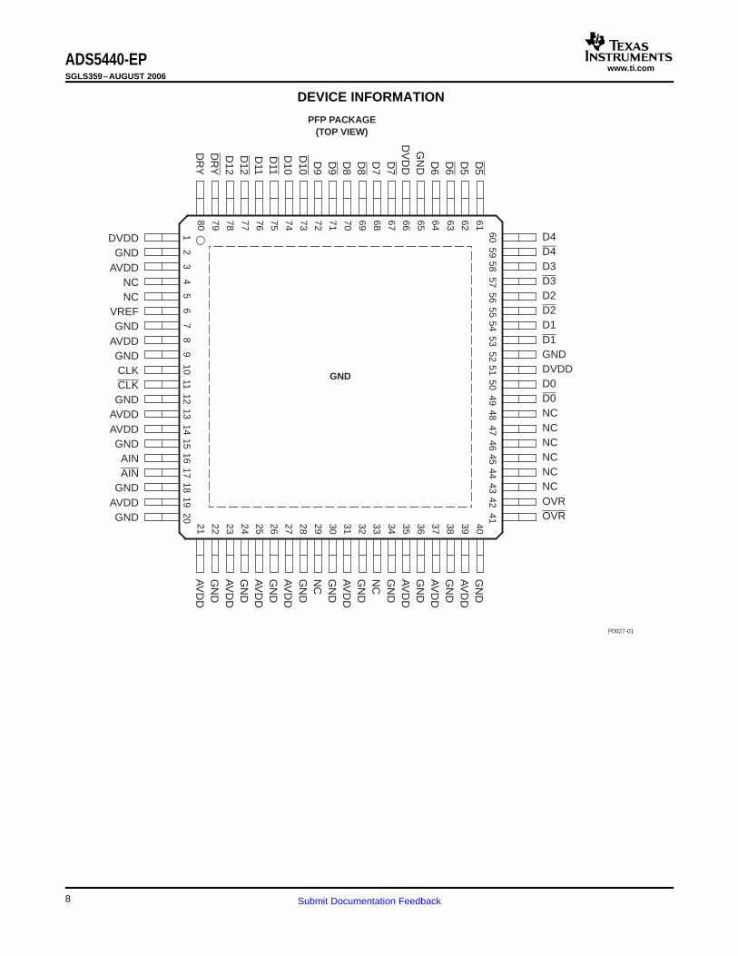
DEVICE INFORMATION
23
GN
DA
VD
DG
ND
AV
DD
GN
DA
VD
DG
ND
NC
GN
DA
VD
DG
ND
NC
GN
DA
VD
DG
ND
AV
DD
GN
DA
VD
DG
ND
AV
DD
40393837363534333231302928272625242322214
6162636465666768697071727374757677787980
D5
D5
D6
D6
GN
DD
VD
DD7
D7
D8
D8
D9
D9
D10
D10
D11
D11
D12
D12
DR
YD
RY
56
78
PFP PACKAGE(TOP VIEW)
5958
5756
5560
5452
5150
53
910
1112
13
4948
1
4746
4544
1415
1617
1819
20
4342
41D4D4D3D3D2D2D1D1GNDDVDDD0D0NCNCNCNCNCNCOVROVR
DVDDGND
AVDDNCNC
VREFGND
AVDDGNDCLKCLKGND
AVDDAVDDGND
AINAIN
GNDAVDDGND
GND
P0027-01
ADS5440-EPSGLS359–AUGUST 2006
8 Submit Documentation Feedback
www.ti.com
DEFINITION OF SPECIFICATIONS
ADS5440-EPSGLS359–AUGUST 2006
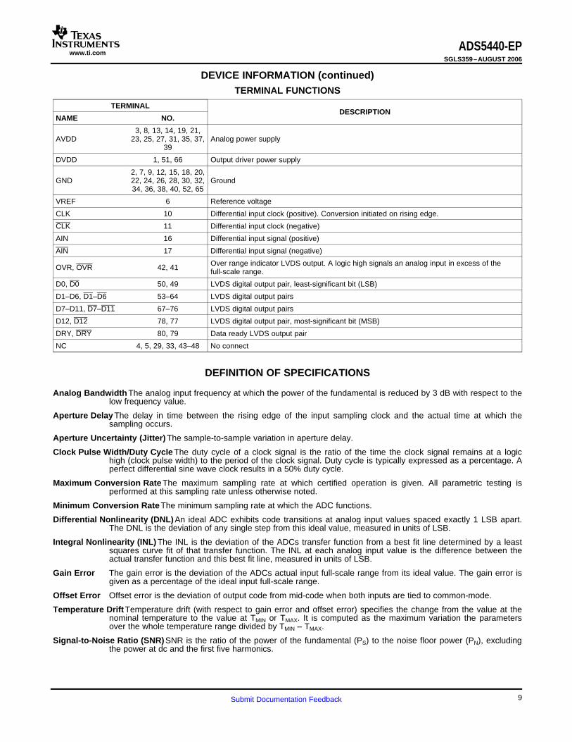
DEVICE INFORMATION (continued)TERMINAL FUNCTIONS
TERMINALDESCRIPTION
NAME NO.
3, 8, 13, 14, 19, 21,AVDD 23, 25, 27, 31, 35, 37, Analog power supply
39
DVDD 1, 51, 66 Output driver power supply
2, 7, 9, 12, 15, 18, 20,GND 22, 24, 26, 28, 30, 32, Ground
34, 36, 38, 40, 52, 65
VREF 6 Reference voltage
CLK 10 Differential input clock (positive). Conversion initiated on rising edge.
CLK 11 Differential input clock (negative)
AIN 16 Differential input signal (positive)
AIN 17 Differential input signal (negative)
Over range indicator LVDS output. A logic high signals an analog input in excess of theOVR, OVR 42, 41 full-scale range.
D0, D0 50, 49 LVDS digital output pair, least-significant bit (LSB)
D1–D6, D1–D6 53–64 LVDS digital output pairs
D7–D11, D7–D11 67–76 LVDS digital output pairs
D12, D12 78, 77 LVDS digital output pair, most-significant bit (MSB)
DRY, DRY 80, 79 Data ready LVDS output pair
NC 4, 5, 29, 33, 43–48 No connect
Analog Bandwidth The analog input frequency at which the power of the fundamental is reduced by 3 dB with respect to thelow frequency value.
Aperture Delay The delay in time between the rising edge of the input sampling clock and the actual time at which thesampling occurs.
Aperture Uncertainty (Jitter) The sample-to-sample variation in aperture delay.
Clock Pulse Width/Duty Cycle The duty cycle of a clock signal is the ratio of the time the clock signal remains at a logichigh (clock pulse width) to the period of the clock signal. Duty cycle is typically expressed as a percentage. Aperfect differential sine wave clock results in a 50% duty cycle.
Maximum Conversion Rate The maximum sampling rate at which certified operation is given. All parametric testing isperformed at this sampling rate unless otherwise noted.
Minimum Conversion Rate The minimum sampling rate at which the ADC functions.
Differential Nonlinearity (DNL) An ideal ADC exhibits code transitions at analog input values spaced exactly 1 LSB apart.The DNL is the deviation of any single step from this ideal value, measured in units of LSB.
Integral Nonlinearity (INL) The INL is the deviation of the ADCs transfer function from a best fit line determined by a leastsquares curve fit of that transfer function. The INL at each analog input value is the difference between theactual transfer function and this best fit line, measured in units of LSB.
Gain Error The gain error is the deviation of the ADCs actual input full-scale range from its ideal value. The gain error isgiven as a percentage of the ideal input full-scale range.
Offset Error Offset error is the deviation of output code from mid-code when both inputs are tied to common-mode.
Temperature Drift Temperature drift (with respect to gain error and offset error) specifies the change from the value at thenominal temperature to the value at TMIN or TMAX. It is computed as the maximum variation the parametersover the whole temperature range divided by TMIN – TMAX.
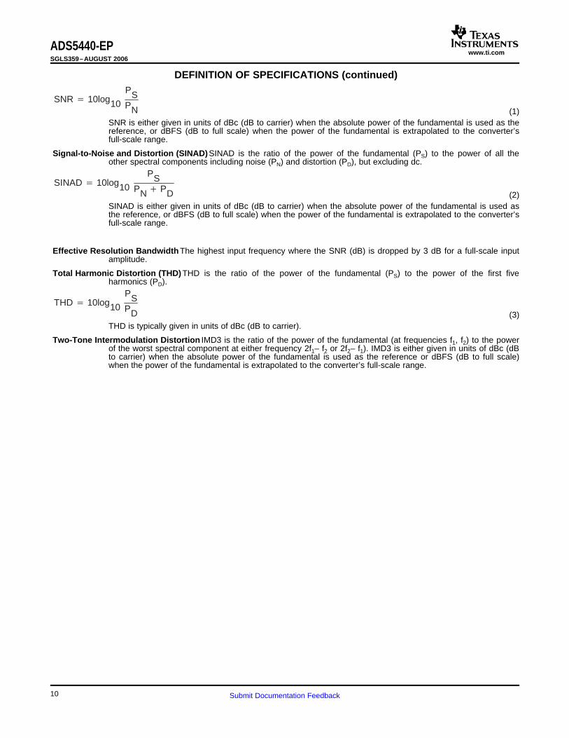
Signal-to-Noise Ratio (SNR)SNR is the ratio of the power of the fundamental (PS) to the noise floor power (PN), excludingthe power at dc and the first five harmonics.
9Submit Documentation Feedback
www.ti.com
SNR 10log10
PSPN (1)
SINAD 10log10
PSPN PD (2)
THD 10log10
PSPD (3)
ADS5440-EPSGLS359–AUGUST 2006
DEFINITION OF SPECIFICATIONS (continued)
SNR is either given in units of dBc (dB to carrier) when the absolute power of the fundamental is used as thereference, or dBFS (dB to full scale) when the power of the fundamental is extrapolated to the converter’sfull-scale range.
Signal-to-Noise and Distortion (SINAD)SINAD is the ratio of the power of the fundamental (PS) to the power of all theother spectral components including noise (PN) and distortion (PD), but excluding dc.
SINAD is either given in units of dBc (dB to carrier) when the absolute power of the fundamental is used asthe reference, or dBFS (dB to full scale) when the power of the fundamental is extrapolated to the converter’sfull-scale range.
Effective Resolution Bandwidth The highest input frequency where the SNR (dB) is dropped by 3 dB for a full-scale inputamplitude.
Total Harmonic Distortion (THD)THD is the ratio of the power of the fundamental (PS) to the power of the first fiveharmonics (PD).
THD is typically given in units of dBc (dB to carrier).
Two-Tone Intermodulation Distortion IMD3 is the ratio of the power of the fundamental (at frequencies f1, f2) to the powerof the worst spectral component at either frequency 2f1– f2 or 2f2– f1). IMD3 is either given in units of dBc (dBto carrier) when the absolute power of the fundamental is used as the reference or dBFS (dB to full scale)when the power of the fundamental is extrapolated to the converter’s full-scale range.
10 Submit Documentation Feedback
www.ti.com
TYPICAL CHARACTERISTICS
f − Frequency − MHz
−120
−100
−80
−60
−40
−20
0
0 10 20 30 40 50 60 70 80 90 100
Am
plitu
de −
dB
G001
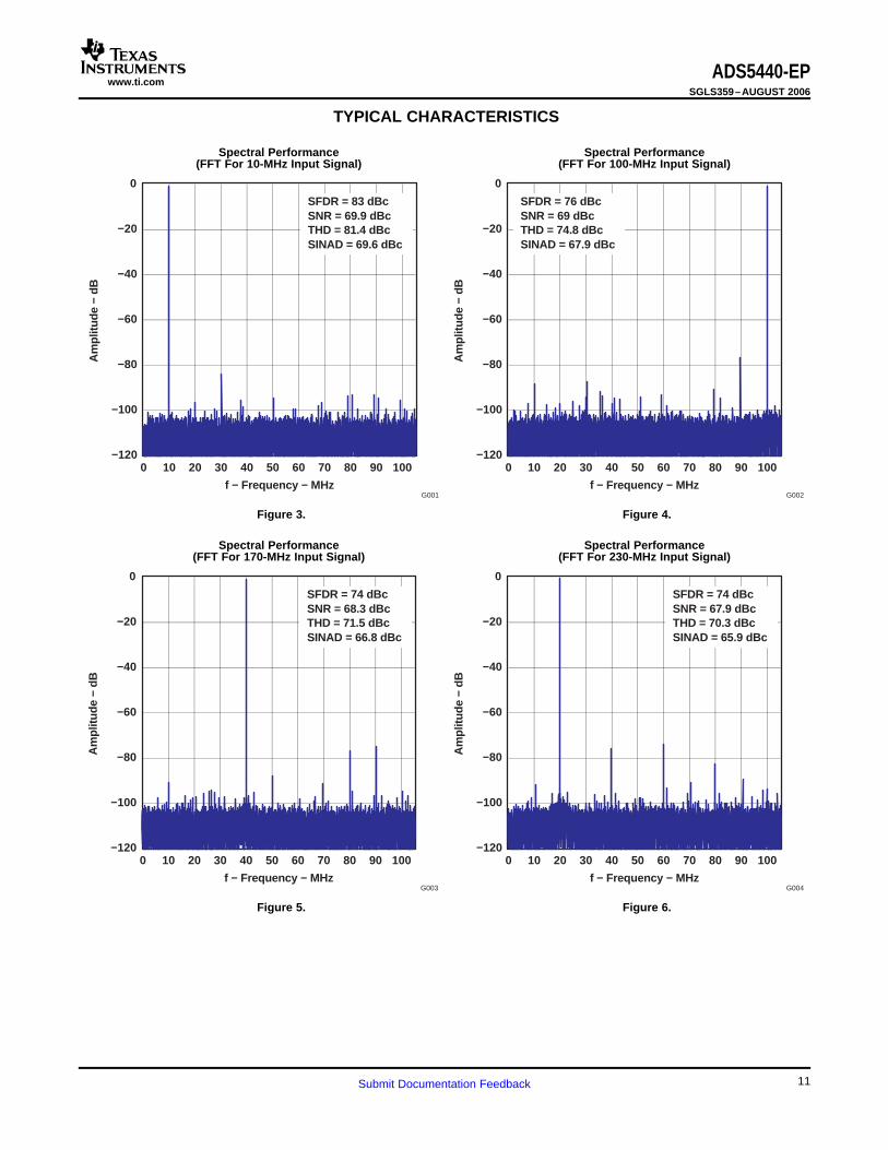
SFDR = 83 dBcSNR = 69.9 dBcTHD = 81.4 dBcSINAD = 69.6 dBc
f − Frequency − MHz
−120
−100
−80
−60
−40
−20
0
0 10 20 30 40 50 60 70 80 90 100
SFDR = 76 dBcSNR = 69 dBcTHD = 74.8 dBcSINAD = 67.9 dBc
Am
plitu
de −
dB
G002
f − Frequency − MHz
−120
−100
−80
−60
−40
−20
0
0 10 20 30 40 50 60 70 80 90 100
Am
plitu
de −
dB
G003
SFDR = 74 dBcSNR = 68.3 dBcTHD = 71.5 dBcSINAD = 66.8 dBc
f − Frequency − MHz
−120
−100
−80
−60
−40
−20
0
0 10 20 30 40 50 60 70 80 90 100
Am
plitu
de −
dB
G004
SFDR = 74 dBcSNR = 67.9 dBcTHD = 70.3 dBcSINAD = 65.9 dBc
ADS5440-EPSGLS359–AUGUST 2006
Spectral Performance Spectral Performance(FFT For 10-MHz Input Signal) (FFT For 100-MHz Input Signal)
Figure 3. Figure 4.
Spectral Performance Spectral Performance(FFT For 170-MHz Input Signal) (FFT For 230-MHz Input Signal)
Figure 5. Figure 6.
11Submit Documentation Feedback
www.ti.com
f − Frequency − MHz
−120
−100
−80
−60
−40
−20
0
0 10 20 30 40 50 60 70 80 90 100
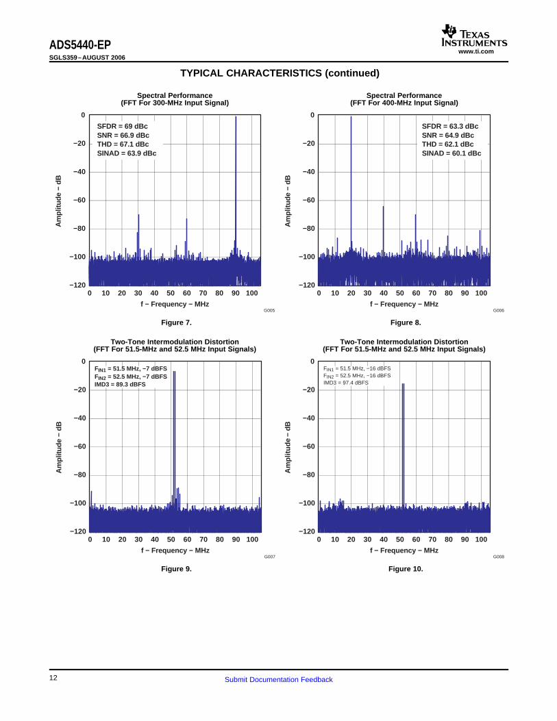
SFDR = 69 dBcSNR = 66.9 dBcTHD = 67.1 dBcSINAD = 63.9 dBc
Am
plitu
de −
dB
G005f − Frequency − MHz
−120
−100
−80
−60
−40
−20
0
0 10 20 30 40 50 60 70 80 90 100A
mpl
itude
− d
B
G006
SFDR = 63.3 dBcSNR = 64.9 dBcTHD = 62.1 dBcSINAD = 60.1 dBc
f − Frequency − MHz
−120
−100
−80
−60
−40
−20
0
0 10 20 30 40 50 60 70 80 90 100
FIN1 = 51.5 MHz, −7 dBFSFIN2 = 52.5 MHz, −7 dBFSIMD3 = 89.3 dBFS
Am
plitu
de −
dB
G007f − Frequency − MHz
−120
−100
−80
−60
−40
−20
0
0 10 20 30 40 50 60 70 80 90 100
FIN1 = 51.5 MHz, −16 dBFSFIN2 = 52.5 MHz, −16 dBFSIMD3 = 97.4 dBFS
Am
plitu
de −
dB
G008
ADS5440-EPSGLS359–AUGUST 2006
TYPICAL CHARACTERISTICS (continued)
Spectral Performance Spectral Performance(FFT For 300-MHz Input Signal) (FFT For 400-MHz Input Signal)
Figure 7. Figure 8.
Two-Tone Intermodulation Distortion Two-Tone Intermodulation Distortion(FFT For 51.5-MHz and 52.5 MHz Input Signals) (FFT For 51.5-MHz and 52.5 MHz Input Signals)
Figure 9. Figure 10.
12 Submit Documentation Feedback
www.ti.com
f − Frequency − MHz
−120
−100
−80
−60
−40
−20
0
0 10 20 30 40 50 60 70 80 90 100
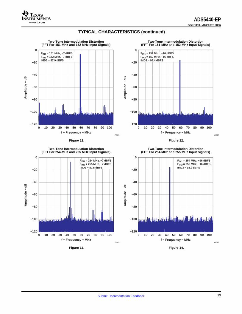
FIN1 = 151 MHz, −7 dBFSFIN2 = 152 MHz, −7 dBFSIMD3 = 87.9 dBFS
Am
plitu
de −
dB
G009f − Frequency − MHz
−120
−100
−80
−60
−40
−20
0
0 10 20 30 40 50 60 70 80 90 100
FIN1 = 151 MHz, −16 dBFSFIN2 = 152 MHz, −16 dBFSIMD3 = 99.4 dBFS
Am
plitu
de −
dB
G010
f − Frequency − MHz
−120
−100
−80
−60
−40
−20
0
0 10 20 30 40 50 60 70 80 90 100
Am
plitu
de −
dB
G011
FIN1 = 254 MHz, −7 dBFSFIN2 = 255 MHz, −7 dBFSIMD3 = 80.5 dBFS
f − Frequency − MHz
−120
−100
−80
−60
−40
−20
0
0 10 20 30 40 50 60 70 80 90 100
Am
plitu
de −
dB
G012
FIN1 = 254 MHz, −16 dBFSFIN2 = 255 MHz, −16 dBFSIMD3 = 93.9 dBFS
ADS5440-EPSGLS359–AUGUST 2006
TYPICAL CHARACTERISTICS (continued)
Two-Tone Intermodulation Distortion Two-Tone Intermodulation Distortion(FFT For 151-MHz and 152 MHz Input Signals) (FFT For 151-MHz and 152 MHz Input Signals)
Figure 11. Figure 12.
Two-Tone Intermodulation Distortion Two-Tone Intermodulation Distortion(FFT For 254-MHz and 255 MHz Input Signals) (FFT For 254-MHz and 255 MHz Input Signals)
Figure 13. Figure 14.
13Submit Documentation Feedback
www.ti.com
f − Frequency − MHz
−120
−100
−80
−60
−40
−20
0
0 10 20 30 40 50 60 70 80 90 100
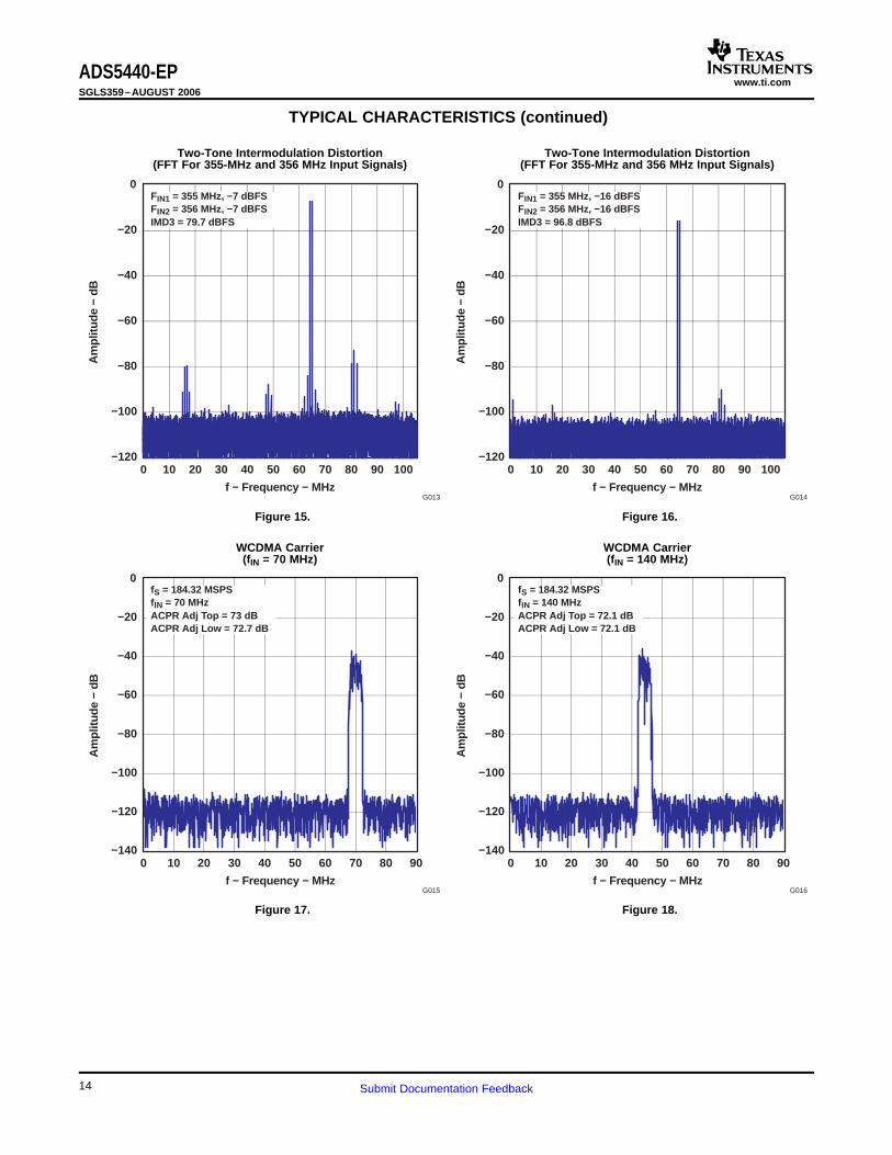
FIN1 = 355 MHz, −7 dBFSFIN2 = 356 MHz, −7 dBFSIMD3 = 79.7 dBFS
Am
plitu
de −
dB
G013f − Frequency − MHz
−120
−100
−80
−60
−40
−20
0
0 10 20 30 40 50 60 70 80 90 100
FIN1 = 355 MHz, −16 dBFSFIN2 = 356 MHz, −16 dBFSIMD3 = 96.8 dBFS
Am
plitu
de −
dB
G014
f − Frequency − MHz
−140
−120
−100
−80
−60
−40
−20
0
0 10 20 30 40 50 60 70 80 90
fS = 184.32 MSPSfIN = 70 MHzACPR Adj T op = 73 dBACPR Adj Low = 72.7 dB
Am
plitu
de −
dB
G015f − Frequency − MHz
−140
−120
−100
−80
−60
−40
−20
0
0 10 20 30 40 50 60 70 80 90
Am
plitu
de −
dB
G016
fS = 184.32 MSPSfIN = 140 MHzACPR Adj T op = 72.1 dBACPR Adj Low = 72.1 dB
ADS5440-EPSGLS359–AUGUST 2006
TYPICAL CHARACTERISTICS (continued)
Two-Tone Intermodulation Distortion Two-Tone Intermodulation Distortion(FFT For 355-MHz and 356 MHz Input Signals) (FFT For 355-MHz and 356 MHz Input Signals)
Figure 15. Figure 16.
WCDMA Carrier WCDMA Carrier(fIN = 70 MHz) (fIN = 140 MHz)
Figure 17. Figure 18.
14 Submit Documentation Feedback
www.ti.com
fIN − Input Frequency − MHz
−10
−9
−8
−7
−6
−5
−4
−3
−2
−1
0
fS = 210 MSPSAIN = −1 dBFS
Inpu
t Am
plitu
de −
dB
G017
1 10 1k100
Code
−0.4
−0.3
−0.2
−0.1
0.0
0.1
0.2
0.3
0.4
0 1024 2048 3072 4096 5120 6144 7168 8192
fS = 210 MSPSfIN = 10 MHz
Diff
eren
tial N
onlin
earit
y −
LSB
G018
Code
−1.0
−0.8
−0.6
−0.4
−0.2
0.0
0.2
0.4
0.6
0.8
1.0
0 1024 2048 3072 4096 5120 6144 7168 8192
fS = 210 MSPSfIN = 10 MHz
INL
− In
tegr
al N
onlin
earit
y −
LSB
G019Code Number
0
5
10
15
20
25
30
35
40
45
4101 4102 4103 4104 4105 4106
Per
cent
age
− %
G020
ADS5440-EPSGLS359–AUGUST 2006
TYPICAL CHARACTERISTICS (continued)
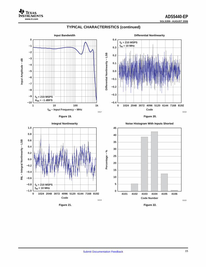
Input Bandwidth Differential Nonlinearity
Figure 19. Figure 20.
Integral Nonlinearity Noise Histogram With Inputs Shorted
Figure 21. Figure 22.
15Submit Documentation Feedback
www.ti.com
Input Amplitude − dBFS
−20
0
20
40
60
80
100
−100 −90 −80 −70 −60 −50 −40 −30 −20 −10 0
fS = 210 MSPSfIN = 100 MHz
Per
form
ance
− d
B
G021
SFDR (dBFS)
SNR (dBFS)
SNR (dBc)
SFDR (dBc)
Input Amplitude − dBFS
−20
0
20
40
60
80
100
−100 −90 −80 −70 −60 −50 −40 −30 −20 −10 0
fS = 210 MSPSfIN = 230 MHz
Per
form
ance
− d
B
G022
SFDR (dBFS)
SNR (dBFS)
SNR (dBc)
SFDR (dBc)
Input Amplitude − dBFS
−20
0
20
40
60
80
100
120
−110−100 −90 −80 −70 −60 −50 −40 −30 −20 −10 0
fS = 210 MSPSf1 = 151 MHzf2 = 152 MHzS
FD
R −
Spu
rious
-Fre
e D
ynam
ic R
ange
− d
B
G023
SFDR (dBFS)
90 dBFS Line
SFDR (dBc)
Duty Cycle − %
60.0
62.5
65.0
67.5
70.0
72.5
75.0
77.5
80.0
40 45 50 55 60
fS = 210 MSPS Square Wave
SF
DR
− S
purio
us-F
ree
Dyn
amic
Ran
ge −
dB
c
G024
fIN = 100.33 MHz
fIN = 230.13 MHz
ADS5440-EPSGLS359–AUGUST 2006
TYPICAL CHARACTERISTICS (continued)
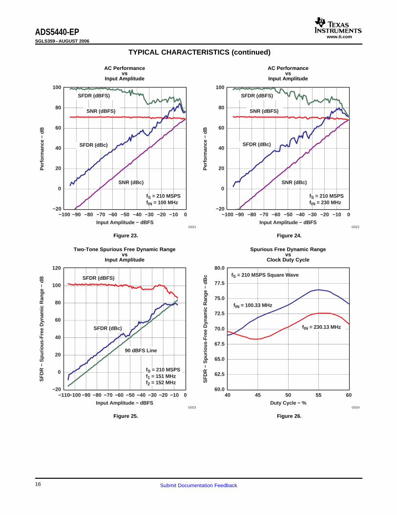
AC Performance AC Performancevs vs
Input Amplitude Input Amplitude
Figure 23. Figure 24.
Two-Tone Spurious Free Dynamic Range Spurious Free Dynamic Rangevs vs
Input Amplitude Clock Duty Cycle
Figure 25. Figure 26.
16 Submit Documentation Feedback
www.ti.com
Clock Amplitude − V P−P
60
61
62
63
64
65
66
67
68
69
70
0.0 0.5 1.0 1.5 2.0 2.5 3.0 3.5 4.0
SN
R −
Sig
nal-t
o-N
oise
Rat
io −
dB
c
G026
fS = 210 MSPS fIN = 100.33 MHz
fIN = 230.13 MHz
Clock Amplitude − V P−P
60
62
64
66
68
70
72
74
76
78
0.0 0.5 1.0 1.5 2.0 2.5 3.0 3.5 4.0
SF
DR
− S
purio
us-F
ree
Dyn
amic
Ran
ge −
dB
c
G025
fS = 210 MSPSfIN = 100.33 MHz
fIN = 230.13 MHz
Clock Common-Mode V oltage − V
10
20
30
40
50
60
70
80
0 1 2 3 4 5
Per
form
ance
− d
Bc
G027
SFDR
SNR
fs = 210 MSPSfin = 100 MHz
AVDD − Supply V oltage − V
70
72
74
76
78
80
82
84
4.65 4.75 4.85 4.95 5.05 5.15 5.25 5.35
SF
DR
− S
purio
us-F
ree
Dyn
amic
Ran
ge −
dB
c
G028
fS = 210 MSPSfIN = 100 MHz
TA = −40°C
TA = 0°CTA = 25°C
TA = 65°C
TA = 85°C
ADS5440-EPSGLS359–AUGUST 2006
TYPICAL CHARACTERISTICS (continued)
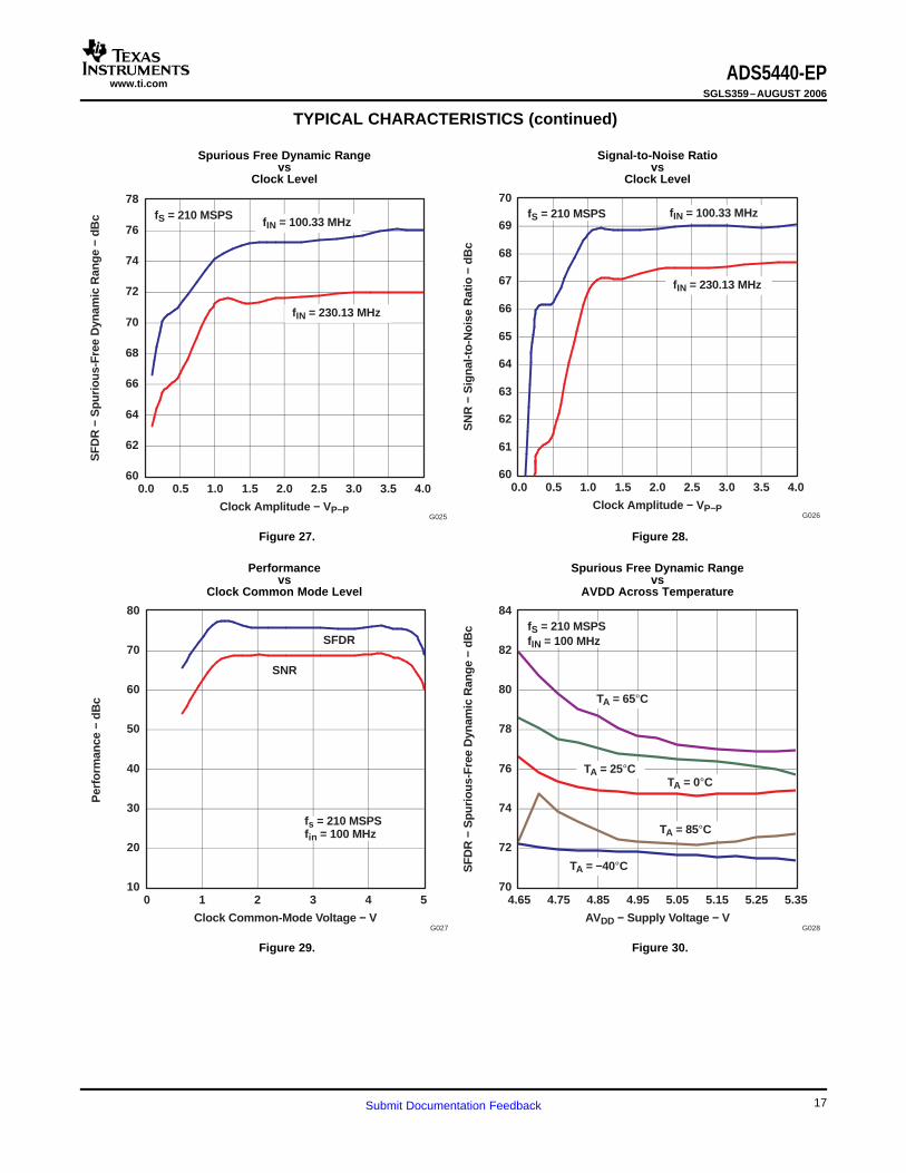
Spurious Free Dynamic Range Signal-to-Noise Ratiovs vs
Clock Level Clock Level
Figure 27. Figure 28.
Performance Spurious Free Dynamic Rangevs vs
Clock Common Mode Level AVDD Across Temperature
Figure 29. Figure 30.
17Submit Documentation Feedback
www.ti.com
AVDD − Supply V oltage − V
65
66
67
68
69
70
4.70 4.80 4.90 5.00 5.10 5.20 5.30
SN
R −
Sig
nal-t
o-N
oise
Rat
io −
dB
c
G029
fS = 210 MSPSfIN = 100 MHz
TA = 0°C
TA = 65°C
TA = 85°CTA = 25°C
TA = −40°C
DRVDD − Supply V oltage − V
70
71
72
73
74
75
76
77
78
79
80
2.9 3.1 3.3 3.5 3.7
SF
DR
− S
purio
us-F
ree
Dyn
amic
Ran
ge −
dB
c
G030
fS = 210 MSPSfIN = 100 MHz
TA = −40°C
TA = 0°C
TA = 25°C
TA = 65°C
TA = 85°C
DRVDD − Supply V oltage − V
65
66
67
68
69
70
3.0 3.1 3.2 3.3 3.4 3.5 3.6 3.7
SN
R −
Sig
nal-t
o-N
oise
Rat
io −
dB
c
G031
fS = 210 MSPSfIN = 100 MHz
TA = 0°C
TA = 65°C
TA = 85°CTA = 25°C
TA = −40°C
ADS5440-EPSGLS359–AUGUST 2006
TYPICAL CHARACTERISTICS (continued)
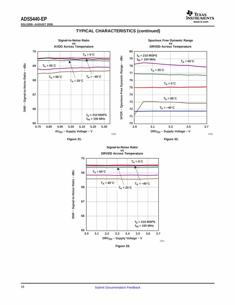
Signal-to-Noise Ratio Spurious Free Dynamic Rangevs vs
AVDD Across Temperature DRVDD Across Temperature
Figure 31. Figure 32.
Signal-to-Noise Ratiovs
DRVDD Across Temperature
Figure 33.
18 Submit Documentation Feedback
www.ti.com
54 56 58 60 62 64 70
SNR − dBc
f S −
Sam
plin
g F
requ
ency
− M
Hz
120
80
60
40
20
fIN − Input Frequency − MHz
10 50 250 300 350 400200100 150
100
M0048−01
10
140
160
200
180
220
240
66 68
69
6969
69
68
68
68
68
67
67
67
6766
66
66
66
6665
65
65
65
65 64
64
6463
6363 62
62
6261
61 6060 59
59 58 58 57 56
ADS5440-EPSGLS359–AUGUST 2006
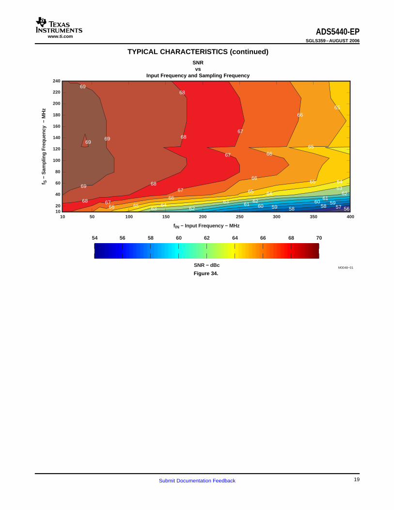
TYPICAL CHARACTERISTICS (continued)SNRvs
Input Frequency and Sampling Frequency
Figure 34.
19Submit Documentation Feedback
www.ti.com
55 60 65 70 75 85
SFDR − dBc
f S −
Sam
plin
g F
requ
ency
− M
Hz
120
80
60
40
20
fIN − Input Frequency − MHz
10 50 250 300 350 400200100 150
100
M0048−02
10
140
160
200
180
220
240
80
72 72
72
72 7068
66
64 62 6058
62
6466
68
6866
70
70
747678808282
84
86
76
76
74
74
7476
78
78
78
80
80
80
82
82
84
84
848482
82
84
82
ADS5440-EPSGLS359–AUGUST 2006
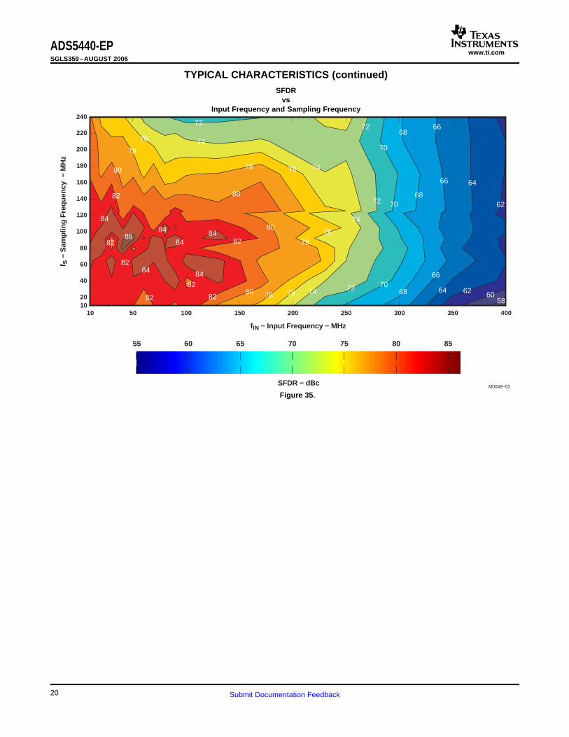
TYPICAL CHARACTERISTICS (continued)SFDR
vsInput Frequency and Sampling Frequency
Figure 35.
20 Submit Documentation Feedback
www.ti.com
APPLICATION INFORMATION
Theory of Operation
Input Configuration
R 0
50Z0
50
1:1
ADT1−1W T
R50
AC Signal
Source
ADS5440
AIN
AIN
RT100 Ω
+
−OPA695
5 V
R1400 Ω
ADS5440CINRIN
0.1 µF1:1
−5 V
R257.5 Ω
VIN
AV = 8V/V(18 dB)
RS100 Ω
1000 µF
RINAIN
AIN
ADS5440-EPSGLS359–AUGUST 2006
The ADS5440 is a 13-bit, 210-MSPS, monolithic pipeline analog-to-digital converter (ADC). Its bipolar analogcore operates from a 5-V supply, while the output uses a 3.3 V supply to provide LVDS compatible outputs. Theconversion process is initiated by the rising edge of the external input clock. At that instant, the differential inputsignal is captured by the input track and hold (T&H) and the input sample is sequentially converted by a seriesof small resolution stages, with the outputs combined in a digital correction logic block. Both the rising and thefalling clock edges are used to propagate the sample through the pipeline every half clock cycle. This processresults in a data latency of four clock cycles, after which the output data is available as a 13-bit parallel word,coded in offset binary format.
The analog input for the ADS5440 consists of an analog differential buffer followed by a bipolar T&H. Theanalog buffer isolates the source driving the input of the ADC from any internal switching. The input commonmode is set internally through a 500-Ω resistor connected from 2.4 V to each of the inputs. This results in adifferential input impedance of 1 kΩ.
For a full-scale differential input, each of the differential lines of the input signal (pins 16 and 17) swingssymmetrically between 2.4 + 0.55 V and 2.4 – 0.55 V. This means that each input has a maximum signal swingof 1.1 VPP for a total differential input signal swing of 2.2 VPP. The maximum swing is determined by the internalreference voltage generator eliminating the need for any external circuitry for this purpose.
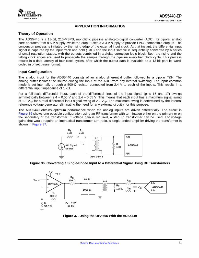
The ADS5440 obtains optimum performance when the analog inputs are driven differentially. The circuit inFigure 36 shows one possible configuration using an RF transformer with termination either on the primary or onthe secondary of the transformer. If voltage gain is required, a step up transformer can be used. For voltagegains that would require an impractical transformer turn ratio, a single-ended amplifier driving the transformer isshown in Figure 37.
Figure 36. Converting a Single-Ended Input to a Differential Signal Using RF Transformers
Figure 37. Using the OPA695 With the ADS5440
21Submit Documentation Feedback
www.ti.com
18 pF
13-Bit210 MSPS
AIN
AIN VREF
ADS5440
+ 5 V
THS4509
CM
348 Ω
348 Ω
100 Ω
100 Ω
78.9 Ω
VINFrom50 Ω
Source
49.9 Ω
49.9 Ω
78.9 Ω 49.9 Ω49.9 Ω
0.22 µF 0.22 µF 0.1 µF 0.1 µF
0.22 µF
Clock Inputs
CLK
ADS5440
CLK
Square Wave or Sine Wave
0.01 µF
0.01 µF
ADS5440-EPSGLS359–AUGUST 2006
Application Information (continued)
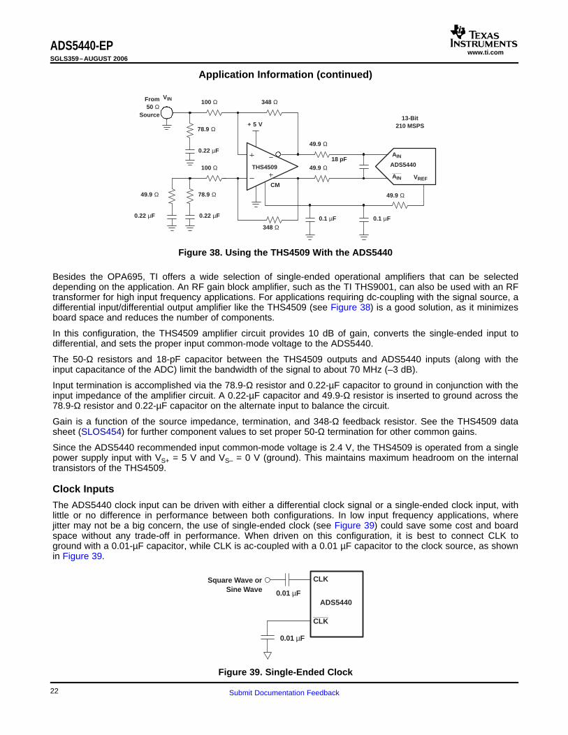
Figure 38. Using the THS4509 With the ADS5440
Besides the OPA695, TI offers a wide selection of single-ended operational amplifiers that can be selecteddepending on the application. An RF gain block amplifier, such as the TI THS9001, can also be used with an RFtransformer for high input frequency applications. For applications requiring dc-coupling with the signal source, adifferential input/differential output amplifier like the THS4509 (see Figure 38) is a good solution, as it minimizesboard space and reduces the number of components.
In this configuration, the THS4509 amplifier circuit provides 10 dB of gain, converts the single-ended input todifferential, and sets the proper input common-mode voltage to the ADS5440.
The 50-Ω resistors and 18-pF capacitor between the THS4509 outputs and ADS5440 inputs (along with theinput capacitance of the ADC) limit the bandwidth of the signal to about 70 MHz (–3 dB).
Input termination is accomplished via the 78.9-Ω resistor and 0.22-µF capacitor to ground in conjunction with theinput impedance of the amplifier circuit. A 0.22-µF capacitor and 49.9-Ω resistor is inserted to ground across the78.9-Ω resistor and 0.22-µF capacitor on the alternate input to balance the circuit.
Gain is a function of the source impedance, termination, and 348-Ω feedback resistor. See the THS4509 datasheet (SLOS454) for further component values to set proper 50-Ω termination for other common gains.
Since the ADS5440 recommended input common-mode voltage is 2.4 V, the THS4509 is operated from a singlepower supply input with VS+ = 5 V and VS– = 0 V (ground). This maintains maximum headroom on the internaltransistors of the THS4509.
The ADS5440 clock input can be driven with either a differential clock signal or a single-ended clock input, withlittle or no difference in performance between both configurations. In low input frequency applications, wherejitter may not be a big concern, the use of single-ended clock (see Figure 39) could save some cost and boardspace without any trade-off in performance. When driven on this configuration, it is best to connect CLK toground with a 0.01-µF capacitor, while CLK is ac-coupled with a 0.01 µF capacitor to the clock source, as shownin Figure 39.
Figure 39. Single-Ended Clock
22 Submit Documentation Feedback
www.ti.com
CLK
ADS5440
CLK
0.1 µF1:4Clock
Source
MA3X71600LCT−ND
CLK
ADS5440
CLK
D
VBB
MC100EP16DT
50 Ω
100 nF
100 nF
50 Ω
113 Ω
Q
Q
D
100 nF
100 nF
100 nF
499 499
Digital Outputs
ADS5440-EPSGLS359–AUGUST 2006
Application Information (continued)
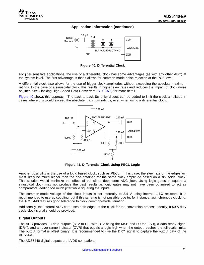
Figure 40. Differential Clock
For jitter-sensitive applications, the use of a differential clock has some advantages (as with any other ADC) atthe system level. The first advantage is that it allows for common-mode noise rejection at the PCB level.
A differential clock also allows for the use of bigger clock amplitudes without exceeding the absolute maximumratings. In the case of a sinusoidal clock, this results in higher slew rates and reduces the impact of clock noiseon jitter. See Clocking High Speed Data Converters (SLYT075) for more detail.
Figure 40 shows this approach. The back-to-back Schottky diodes can be added to limit the clock amplitude incases where this would exceed the absolute maximum ratings, even when using a differential clock.
Figure 41. Differential Clock Using PECL Logic
Another possibility is the use of a logic based clock, such as PECL. In this case, the slew rate of the edges willmost likely be much higher than the one obtained for the same clock amplitude based on a sinusoidal clock.This solution would minimize the effect of the slope dependent ADC jitter. Using logic gates to square asinusoidal clock may not produce the best results as logic gates may not have been optimized to act ascomparators, adding too much jitter while squaring the inputs.
The common-mode voltage of the clock inputs is set internally to 2.4 V using internal 1-kΩ resistors. It isrecommended to use ac coupling, but if this scheme is not possible due to, for instance, asynchronous clocking,the ADS5440 features good tolerance to clock common-mode variation.
Additionally, the internal ADC core uses both edges of the clock for the conversion process. Ideally, a 50% dutycycle clock signal should be provided.
The ADC provides 13 data outputs (D12 to D0, with D12 being the MSB and D0 the LSB), a data-ready signal(DRY), and an over-range indicator (OVR) that equals a logic high when the output reaches the full-scale limits.The output format is offset binary. It is recommended to use the DRY signal to capture the output data of theADS5440.
The ADS5440 digital outputs are LVDS compatible.
23Submit Documentation Feedback
www.ti.com
Power Supplies
Layout Information
PowerPAD™ Package
Assembly Process
ADS5440-EPSGLS359–AUGUST 2006
Application Information (continued)
The use of low noise power supplies with adequate decoupling is recommended. Linear supplies are thepreferred choice versus switched ones, which tend to generate more noise components that can be coupled tothe ADS5440.
The ADS5440 uses two power supplies. For the analog portion of the design, a 5-V AVDD is used, while for thedigital outputs supply (DRVDD) we recommend the use of 3.3 V. All the ground pins are marked as GND,although AGND pins and DRGND pins are not tied together inside the package.
The evaluation board represents a good guideline of how to layout the board to obtain the maximumperformance out of the ADS5440. General design rules as the use of multilayer boards, single ground plane forADC ground connections and local decoupling ceramic chip capacitors should be applied. The input tracesshould be isolated from any external source of interference or noise including the digital outputs, as well as theclock traces. The clock signal traces should also be isolated from other signals, especially in applications wherelow jitter is required as high IF sampling.
Besides performance oriented rules, care has to be taken when considering the heat dissipation out of thedevice. The thermal heatsink should be soldered to the board as described in the PowerPad Package section.
The PowerPAD package is a thermally-enhanced standard size IC package designed to eliminate the use ofbulky heatsinks and slugs traditionally used in thermal packages. This package can be easily mounted usingstandard printed circuit board (PCB) assembly techniques, and can be removed and replaced using standardrepair procedures.
The PowerPAD package is designed so that the leadframe die pad (or thermal pad) is exposed on the bottom ofthe IC. This provides an extremely low thermal resistance path between the die and the exterior of the package.The thermal pad on the bottom of the IC can then be soldered directly to the PCB using the PCB as a heatsink.
1. Prepare the PCB top-side etch pattern including etch for the leads, as well as the thermal pad as illustratedin the Mechanical Data section.
2. Place a 6-by-6 array of thermal vias in the thermal pad area. These holes should be 13 mils in diameter.The small size prevents wicking of the solder through the holes.
3. It is recommended to place a small number of 25-mil diameter holes under the package, but outside thethermal pad area to provide an additional heat path.
4. Connect all holes (both those inside and outside the thermal pad area) to an internal copper plane (such asa ground plane).
5. Do not use the typical web or spoke via connection pattern when connecting the thermal vias to the groundplane. The spoke pattern increases the thermal resistance to the ground plane.
6. The top-side solder mask should leave exposed the terminals of the package and the thermal pad area.7. Cover the entire bottom side of the PowerPAD vias to prevent solder wicking.8. Apply solder paste to the exposed thermal pad area and all of the package terminals.
For more detailed information regarding the PowerPAD package and its thermal properties, see either theSLMA004 application brief, PowerPAD Made Easy, or the technical brief, PowerPAD Thermally EnhancedPackage SLMA002.
24 Submit Documentation Feedback
PACKAGE OPTION ADDENDUM
www.ti.com 31-May-2014
Addendum-Page 1
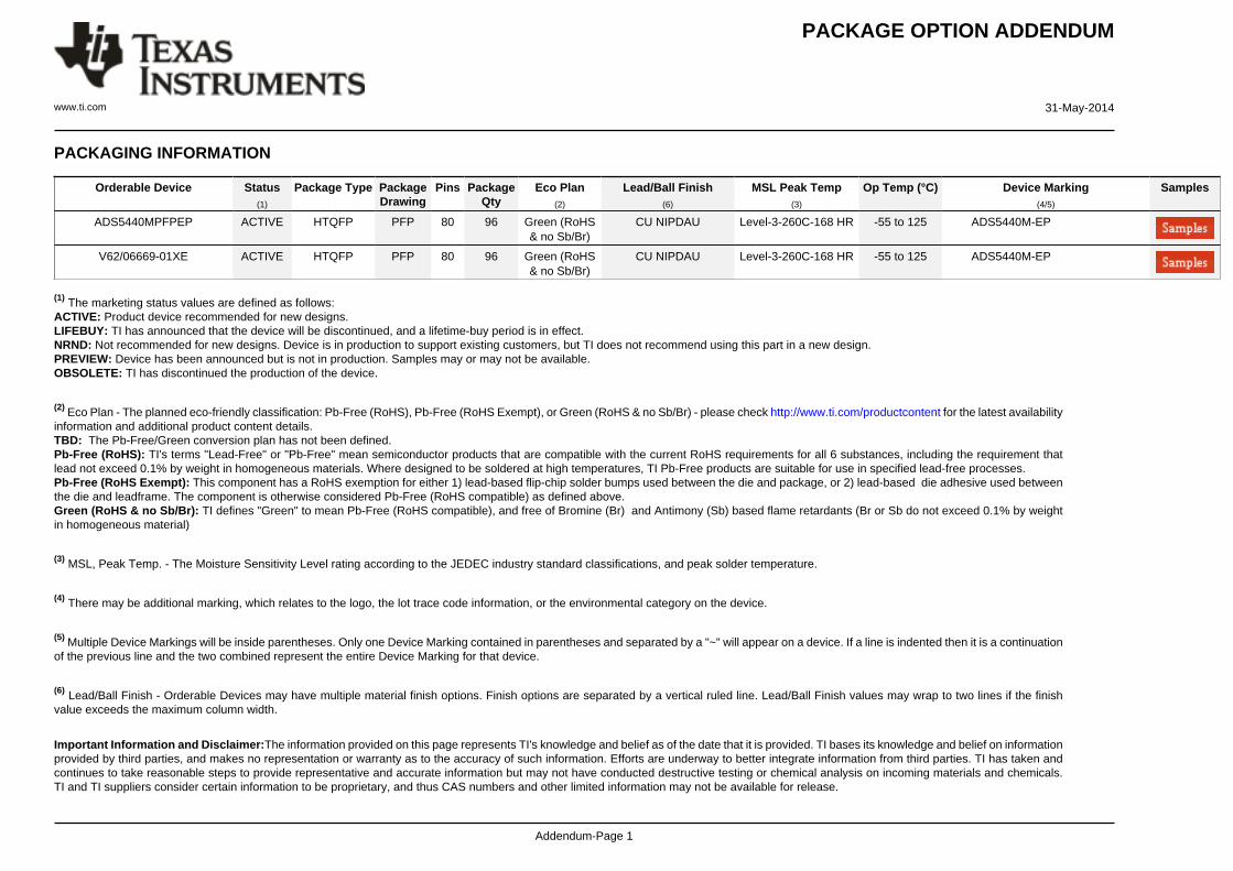
PACKAGING INFORMATION
Orderable Device Status(1)
Package Type PackageDrawing
Pins PackageQty
Eco Plan(2)
Lead/Ball Finish(6)
MSL Peak Temp(3)
Op Temp (°C) Device Marking(4/5)
Samples
ADS5440MPFPEP ACTIVE HTQFP PFP 80 96 Green (RoHS& no Sb/Br)
CU NIPDAU Level-3-260C-168 HR -55 to 125 ADS5440M-EP
V62/06669-01XE ACTIVE HTQFP PFP 80 96 Green (RoHS& no Sb/Br)
CU NIPDAU Level-3-260C-168 HR -55 to 125 ADS5440M-EP
(1) The marketing status values are defined as follows:ACTIVE: Product device recommended for new designs.LIFEBUY: TI has announced that the device will be discontinued, and a lifetime-buy period is in effect.NRND: Not recommended for new designs. Device is in production to support existing customers, but TI does not recommend using this part in a new design.PREVIEW: Device has been announced but is not in production. Samples may or may not be available.OBSOLETE: TI has discontinued the production of the device.
(2) Eco Plan - The planned eco-friendly classification: Pb-Free (RoHS), Pb-Free (RoHS Exempt), or Green (RoHS & no Sb/Br) - please check http://www.ti.com/productcontent for the latest availabilityinformation and additional product content details.TBD: The Pb-Free/Green conversion plan has not been defined.Pb-Free (RoHS): TI's terms "Lead-Free" or "Pb-Free" mean semiconductor products that are compatible with the current RoHS requirements for all 6 substances, including the requirement thatlead not exceed 0.1% by weight in homogeneous materials. Where designed to be soldered at high temperatures, TI Pb-Free products are suitable for use in specified lead-free processes.Pb-Free (RoHS Exempt): This component has a RoHS exemption for either 1) lead-based flip-chip solder bumps used between the die and package, or 2) lead-based die adhesive used betweenthe die and leadframe. The component is otherwise considered Pb-Free (RoHS compatible) as defined above.Green (RoHS & no Sb/Br): TI defines "Green" to mean Pb-Free (RoHS compatible), and free of Bromine (Br) and Antimony (Sb) based flame retardants (Br or Sb do not exceed 0.1% by weightin homogeneous material)
(3) MSL, Peak Temp. - The Moisture Sensitivity Level rating according to the JEDEC industry standard classifications, and peak solder temperature.
(4) There may be additional marking, which relates to the logo, the lot trace code information, or the environmental category on the device.
(5) Multiple Device Markings will be inside parentheses. Only one Device Marking contained in parentheses and separated by a "~" will appear on a device. If a line is indented then it is a continuationof the previous line and the two combined represent the entire Device Marking for that device.
(6) Lead/Ball Finish - Orderable Devices may have multiple material finish options. Finish options are separated by a vertical ruled line. Lead/Ball Finish values may wrap to two lines if the finishvalue exceeds the maximum column width.
Important Information and Disclaimer:The information provided on this page represents TI's knowledge and belief as of the date that it is provided. TI bases its knowledge and belief on informationprovided by third parties, and makes no representation or warranty as to the accuracy of such information. Efforts are underway to better integrate information from third parties. TI has taken andcontinues to take reasonable steps to provide representative and accurate information but may not have conducted destructive testing or chemical analysis on incoming materials and chemicals.TI and TI suppliers consider certain information to be proprietary, and thus CAS numbers and other limited information may not be available for release.
PACKAGE OPTION ADDENDUM
www.ti.com 31-May-2014
Addendum-Page 2
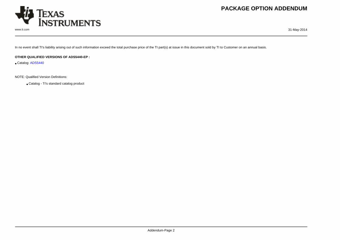
In no event shall TI's liability arising out of such information exceed the total purchase price of the TI part(s) at issue in this document sold by TI to Customer on an annual basis.
OTHER QUALIFIED VERSIONS OF ADS5440-EP :
• Catalog: ADS5440
NOTE: Qualified Version Definitions:
• Catalog - TI's standard catalog product
IMPORTANT NOTICE
Texas Instruments Incorporated and its subsidiaries (TI) reserve the right to make corrections, enhancements, improvements and otherchanges to its semiconductor products and services per JESD46, latest issue, and to discontinue any product or service per JESD48, latestissue. Buyers should obtain the latest relevant information before placing orders and should verify that such information is current andcomplete. All semiconductor products (also referred to herein as “components”) are sold subject to TI’s terms and conditions of salesupplied at the time of order acknowledgment.TI warrants performance of its components to the specifications applicable at the time of sale, in accordance with the warranty in TI’s termsand conditions of sale of semiconductor products. Testing and other quality control techniques are used to the extent TI deems necessaryto support this warranty. Except where mandated by applicable law, testing of all parameters of each component is not necessarilyperformed.TI assumes no liability for applications assistance or the design of Buyers’ products. Buyers are responsible for their products andapplications using TI components. To minimize the risks associated with Buyers’ products and applications, Buyers should provideadequate design and operating safeguards.TI does not warrant or represent that any license, either express or implied, is granted under any patent right, copyright, mask work right, orother intellectual property right relating to any combination, machine, or process in which TI components or services are used. Informationpublished by TI regarding third-party products or services does not constitute a license to use such products or services or a warranty orendorsement thereof. Use of such information may require a license from a third party under the patents or other intellectual property of thethird party, or a license from TI under the patents or other intellectual property of TI.Reproduction of significant portions of TI information in TI data books or data sheets is permissible only if reproduction is without alterationand is accompanied by all associated warranties, conditions, limitations, and notices. TI is not responsible or liable for such altereddocumentation. Information of third parties may be subject to additional restrictions.Resale of TI components or services with statements different from or beyond the parameters stated by TI for that component or servicevoids all express and any implied warranties for the associated TI component or service and is an unfair and deceptive business practice.TI is not responsible or liable for any such statements.Buyer acknowledges and agrees that it is solely responsible for compliance with all legal, regulatory and safety-related requirementsconcerning its products, and any use of TI components in its applications, notwithstanding any applications-related information or supportthat may be provided by TI. Buyer represents and agrees that it has all the necessary expertise to create and implement safeguards whichanticipate dangerous consequences of failures, monitor failures and their consequences, lessen the likelihood of failures that might causeharm and take appropriate remedial actions. Buyer will fully indemnify TI and its representatives against any damages arising out of the useof any TI components in safety-critical applications.In some cases, TI components may be promoted specifically to facilitate safety-related applications. With such components, TI’s goal is tohelp enable customers to design and create their own end-product solutions that meet applicable functional safety standards andrequirements. Nonetheless, such components are subject to these terms.No TI components are authorized for use in FDA Class III (or similar life-critical medical equipment) unless authorized officers of the partieshave executed a special agreement specifically governing such use.Only those TI components which TI has specifically designated as military grade or “enhanced plastic” are designed and intended for use inmilitary/aerospace applications or environments. Buyer acknowledges and agrees that any military or aerospace use of TI componentswhich have not been so designated is solely at the Buyer's risk, and that Buyer is solely responsible for compliance with all legal andregulatory requirements in connection with such use.TI has specifically designated certain components as meeting ISO/TS16949 requirements, mainly for automotive use. In any case of use ofnon-designated products, TI will not be responsible for any failure to meet ISO/TS16949.
Products ApplicationsAudio www.ti.com/audio Automotive and Transportation www.ti.com/automotiveAmplifiers amplifier.ti.com Communications and Telecom www.ti.com/communicationsData Converters dataconverter.ti.com Computers and Peripherals www.ti.com/computersDLP® Products www.dlp.com Consumer Electronics www.ti.com/consumer-appsDSP dsp.ti.com Energy and Lighting www.ti.com/energyClocks and Timers www.ti.com/clocks Industrial www.ti.com/industrialInterface interface.ti.com Medical www.ti.com/medicalLogic logic.ti.com Security www.ti.com/securityPower Mgmt power.ti.com Space, Avionics and Defense www.ti.com/space-avionics-defenseMicrocontrollers microcontroller.ti.com Video and Imaging www.ti.com/videoRFID www.ti-rfid.comOMAP Applications Processors www.ti.com/omap TI E2E Community e2e.ti.comWireless Connectivity www.ti.com/wirelessconnectivity
Mailing Address: Texas Instruments, Post Office Box 655303, Dallas, Texas 75265Copyright © 2016, Texas Instruments Incorporated