Embed Size (px)
Citation preview
Institute of Solid State PhysicsTechnische Universität Graz
13. Bipolar transistors
Jan. 16, 2019
Institute of Solid State Physics
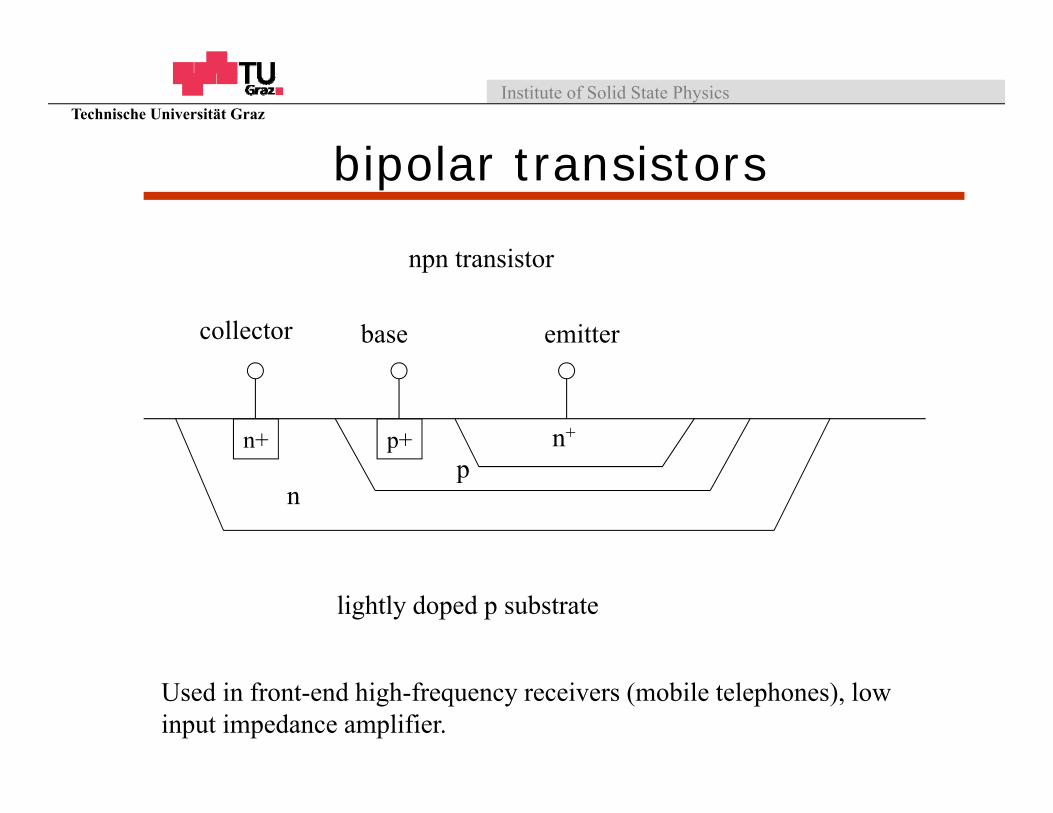
bipolar transistorsTechnische Universität Graz
collector base emitter
np
n+
lightly doped p substrate
npn transistor
Used in front-end high-frequency receivers (mobile telephones), low input impedance amplifier.
p+n+
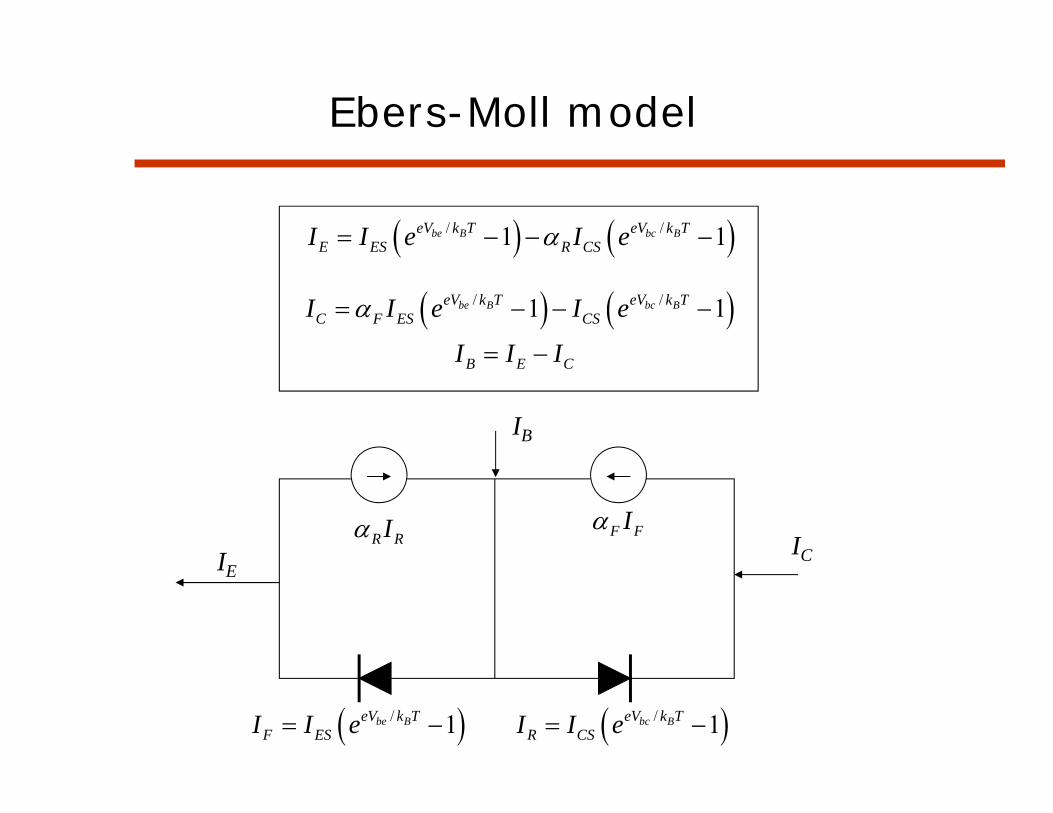
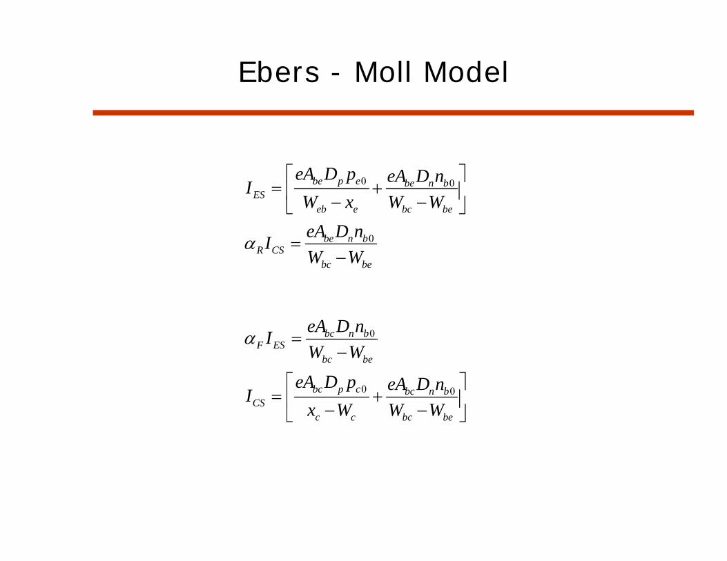
Ebers-Moll model
/ /1 1be B bc BeV k T eV k TC F ES CSI I e I e
/ /1 1be B bc BeV k T eV k TE ES R CSI I e I e
IE
IB
IC
/ 1be BeV k TF ESI I e / 1bc BeV k T
R CSI I e
R RI F FI
B E CI I I
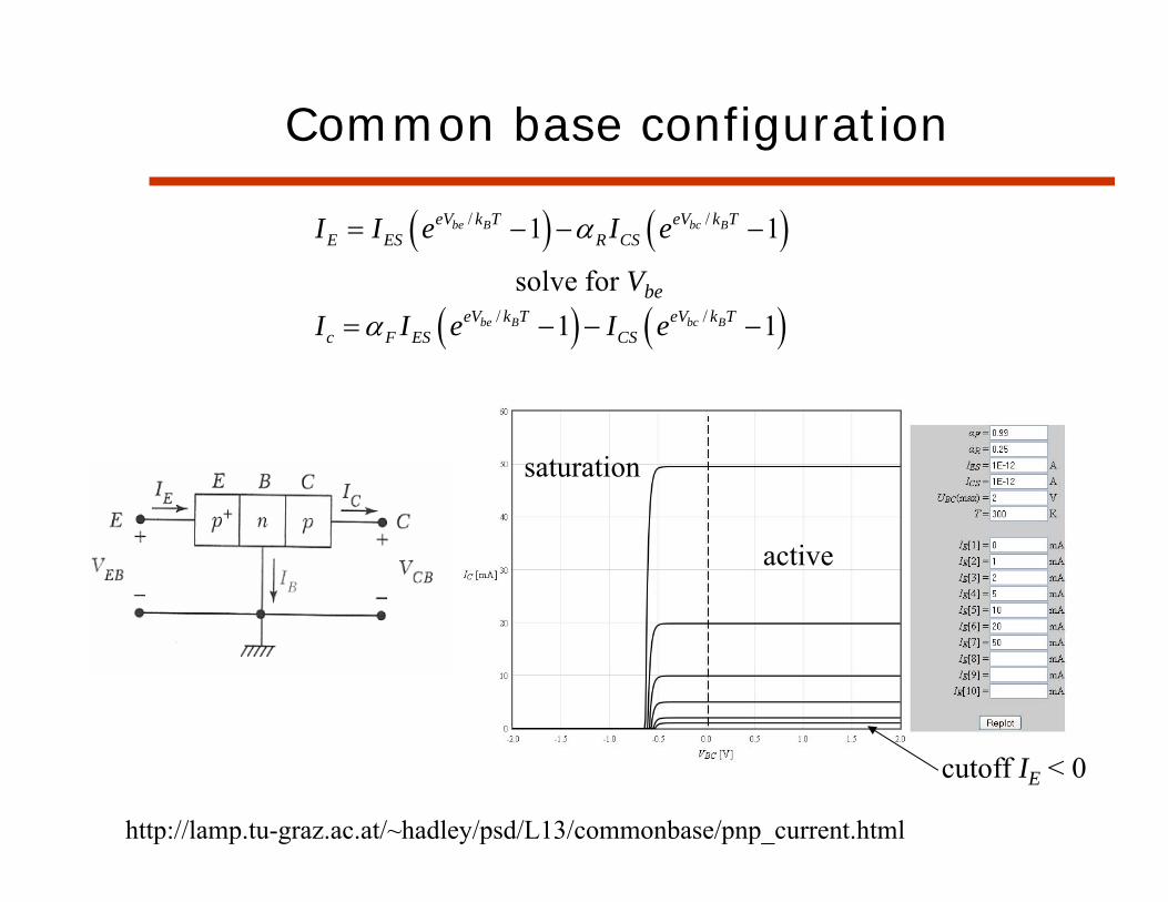
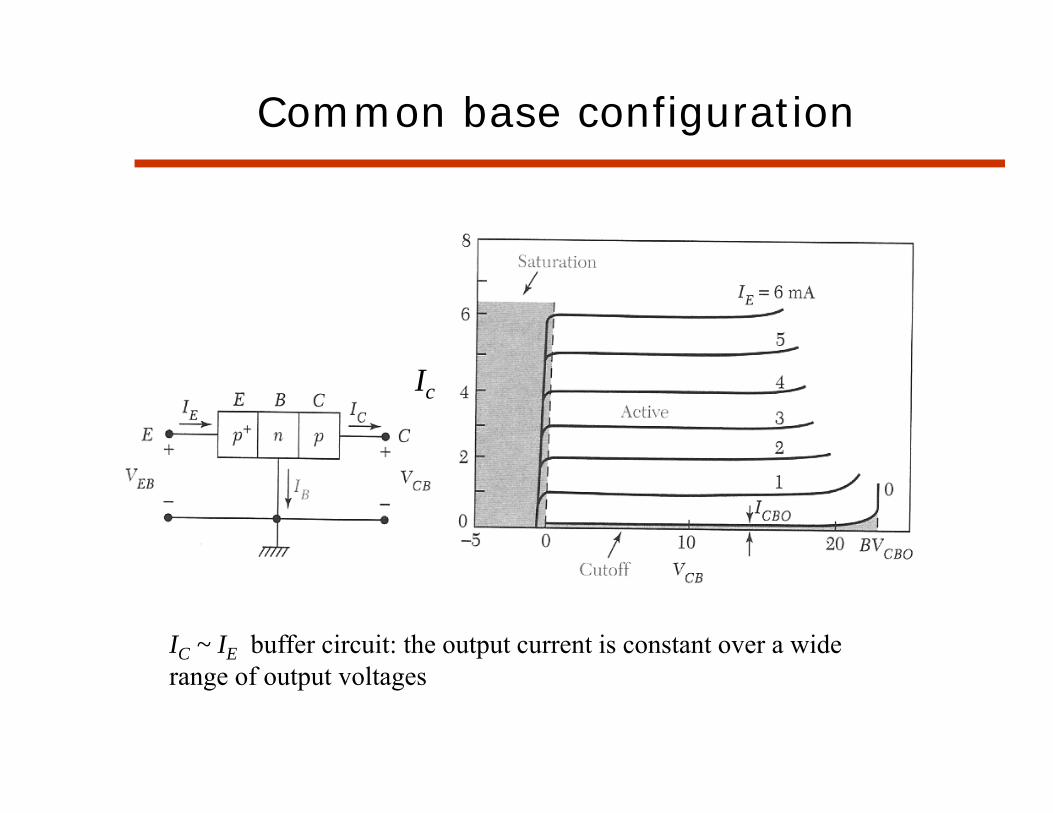
Common base configuration
/ /1 1be B bc BeV k T eV k Tc F ES CSI I e I e
/ /1 1be B bc BeV k T eV k TE ES R CSI I e I e
solve for Vbe
saturation
active
cutoff IE < 0
http://lamp.tu-graz.ac.at/~hadley/psd/L13/commonbase/pnp_current.html
Common base configuration
Ic
IC ~ IE buffer circuit: the output current is constant over a wide range of output voltages
0 0
0
be p e be n bES
eb e bc be
be n bR CS
bc be
eA D p eA D nIW x W WeA D nIW W
Ebers - Moll Model
0
0 0
bc n bF ES
bc be
bc p c bc n bCS
c c bc be
eA D nIW W
eA D p eA D nIx W W W
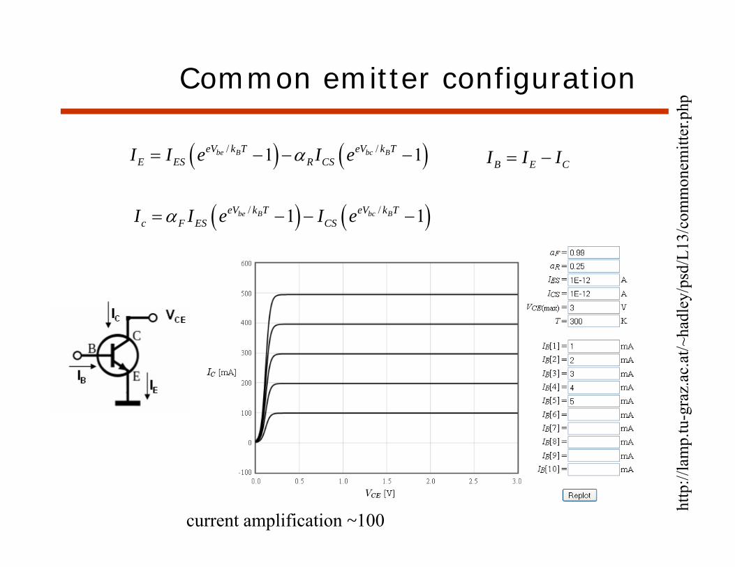
Common emitter configuration
/ /1 1be B bc BeV k T eV k TE ES R CSI I e I e
/ /1 1be B bc BeV k T eV k Tc F ES CSI I e I e
B E CI I I
http
://la
mp.
tu-g
raz.
ac.a
t/~ha
dley
/psd
/L13
/com
mon
emitt
er.p
hp
current amplification ~100
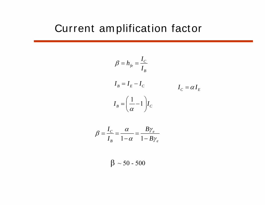
Current amplification factor
Cfe
B
IhI
B E CI I I
1 1B CI I
1 1C e
B e
I BI B
~ 50 - 500
C EI I
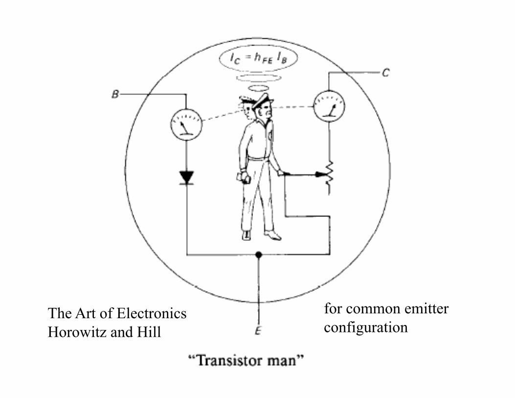
for common emitter configuration
The Art of ElectronicsHorowitz and Hill
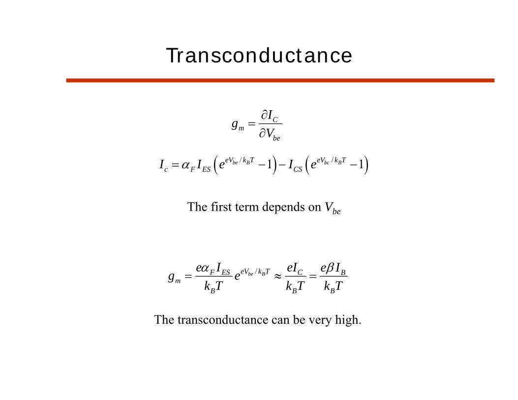
Transconductance
Cm
be
IgV
The transconductance can be very high.
/ /1 1be B bc BeV k T eV k Tc F ES CSI I e I e
/be BeV k TF ES C Bm
B B B
e I eI e Ig ek T k T k T
The first term depends on Vbe
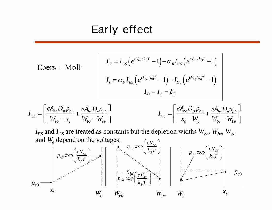
Early effect
/ /1 1be B bc BeV k T eV k Tc F ES CSI I e I e
/ /1 1be B bc BeV k T eV k TE ES R CSI I e I e
B E CI I I
Ebers - Moll:
0 0be p e be n bES
eb e bc be
eA D p eA D nIW x W W
0 0bc p c bc n bCS
c c bc be
eA D p eA D nIx W W W
IES and ICS are treated as constants but the depletion widths Wbc, Wbe, Wc,and We depend on the voltages.
pe0
nb0 pc0
xe We Web WbcxcWc
0 exp beb
B
eVnk T
0 exp bcb
B
eVnk T
0 exp bee
B
eVpk T
0 exp bcc
B
eVpk T
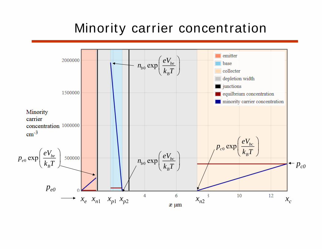
Minority carrier concentration
pe0
pc0
xe xc
0 exp beb
B
eVnk T
0 exp bcb
B
eVnk T
0 exp bee
B
eVpk T
0 exp bcc
B
eVpk T
xn1 xp1 xn2xp2
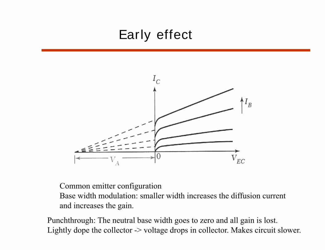
Early effect
Common emitter configurationBase width modulation: smaller width increases the diffusion current and increases the gain.
Punchthrough: The neutral base width goes to zero and all gain is lost.Lightly dope the collector -> voltage drops in collector. Makes circuit slower.
http
://la
mpx
.tugr
az.a
t/~ha
dley
/psd
/L13
/com
mon
_e_e
arly
.php
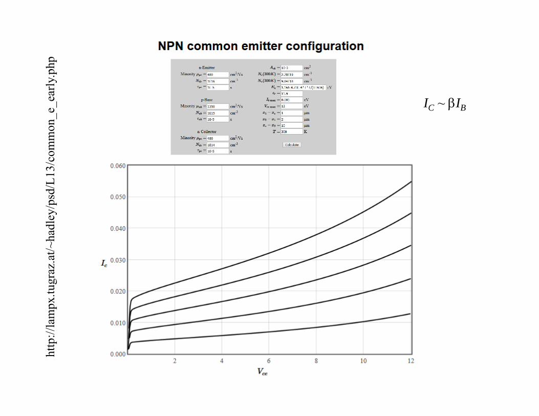
IC ~ IB
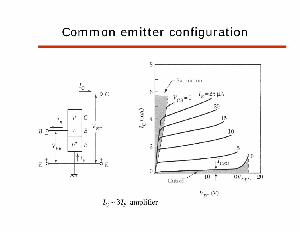
Common emitter configuration
IC ~ IB amplifier
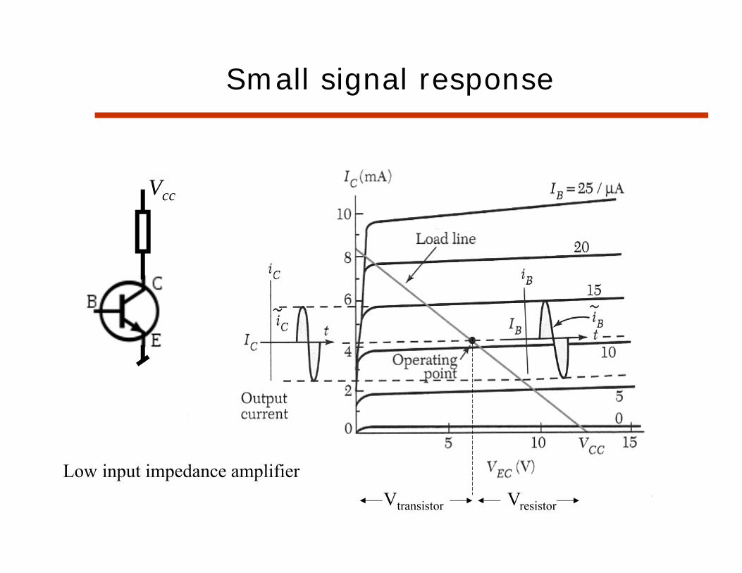
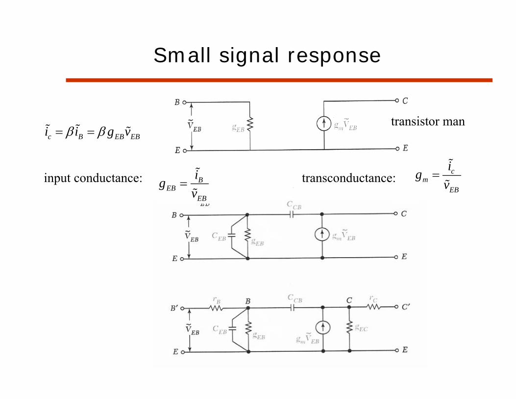
Small signal response
Low input impedance amplifier
Vcc
VresistorVtransistor
Small signal response
input conductance: cm
EB
igv
transconductance:
c B EB EBi i g v transistor man
BEB
EB
igv
Small signal response
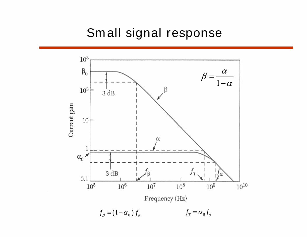
01f f 0Tf f
1
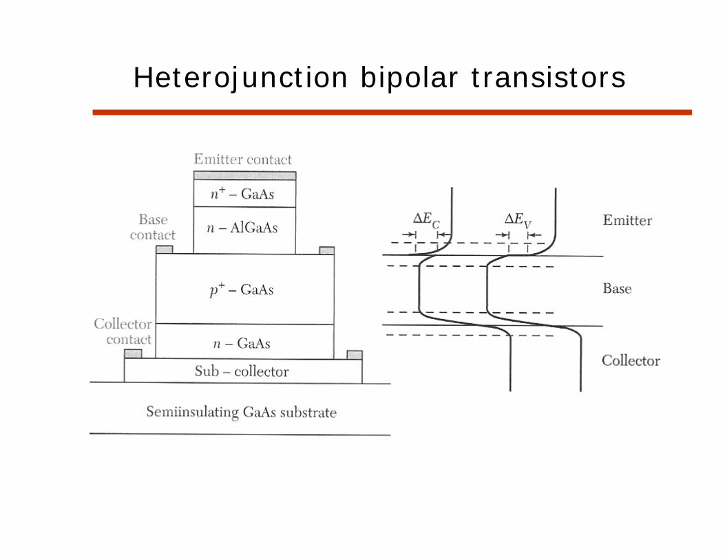
Heterojunction bipolar transistors
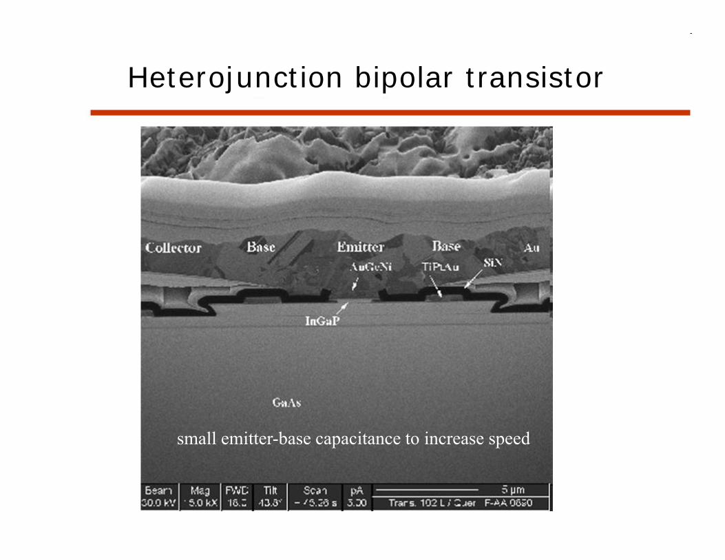
Heterojunction bipolar transistor
small emitter-base capacitance to increase speed
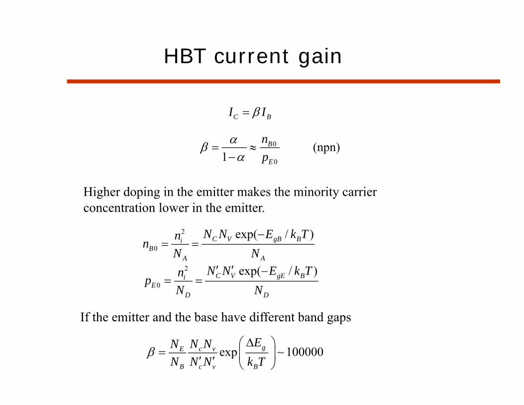
HBT current gain
0
0
(npn)1
B
E
np
C BI I
Higher doping in the emitter makes the minority carrier concentration lower in the emitter.
2
0
exp( / )C V gB BiB
A A
N N E k TnnN N
2
0
exp( / )C V gE BiE
D D
N N E k TnpN N
If the emitter and the base have different band gaps
exp 100000gc vE
B c v B
EN NNN N N k T
HBT current gain
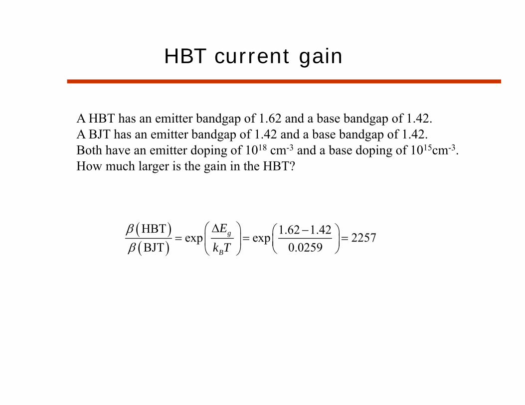
A HBT has an emitter bandgap of 1.62 and a base bandgap of 1.42.A BJT has an emitter bandgap of 1.42 and a base bandgap of 1.42.Both have an emitter doping of 1018 cm-3 and a base doping of 1015cm-3. How much larger is the gain in the HBT?
HBT 1.62 1.42exp exp 2257BJT 0.0259
g
B
Ek T
HBT
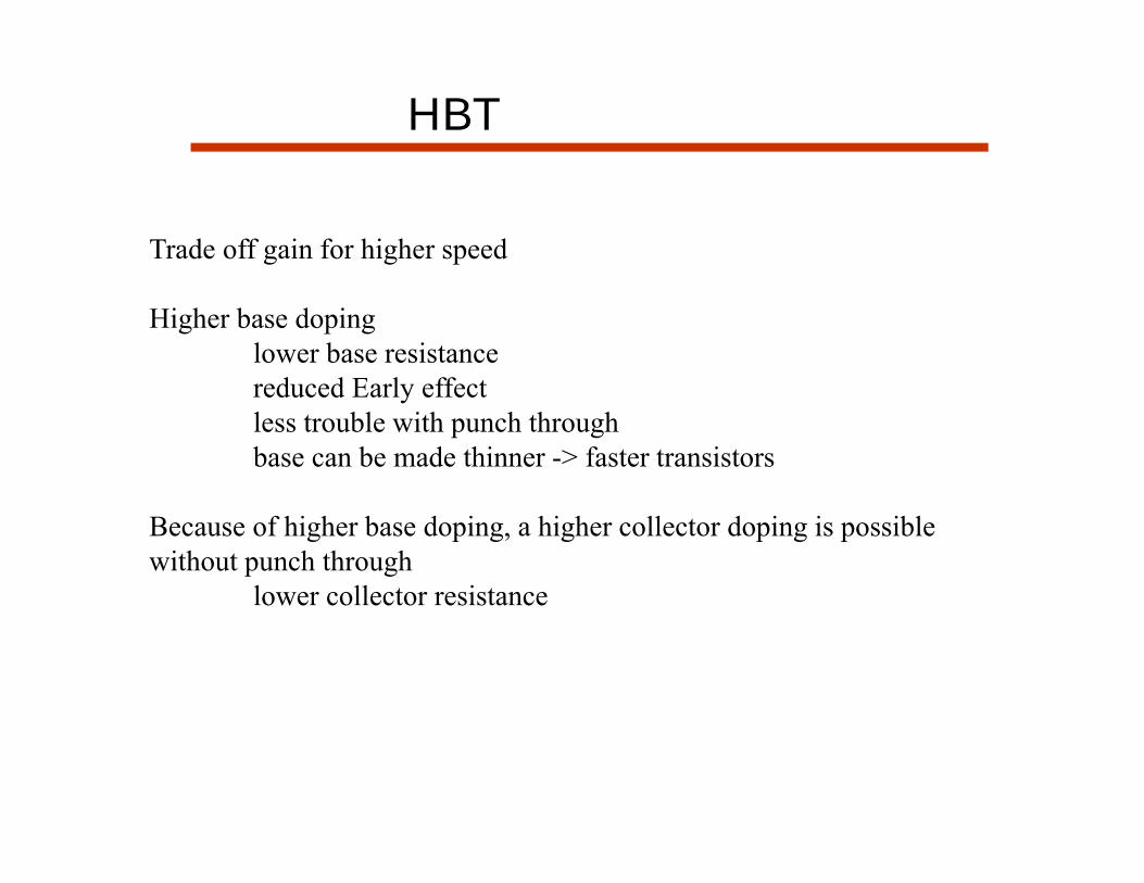
Trade off gain for higher speed
Higher base dopinglower base resistancereduced Early effectless trouble with punch throughbase can be made thinner -> faster transistors
Because of higher base doping, a higher collector doping is possible without punch through
lower collector resistance
HBT current gain
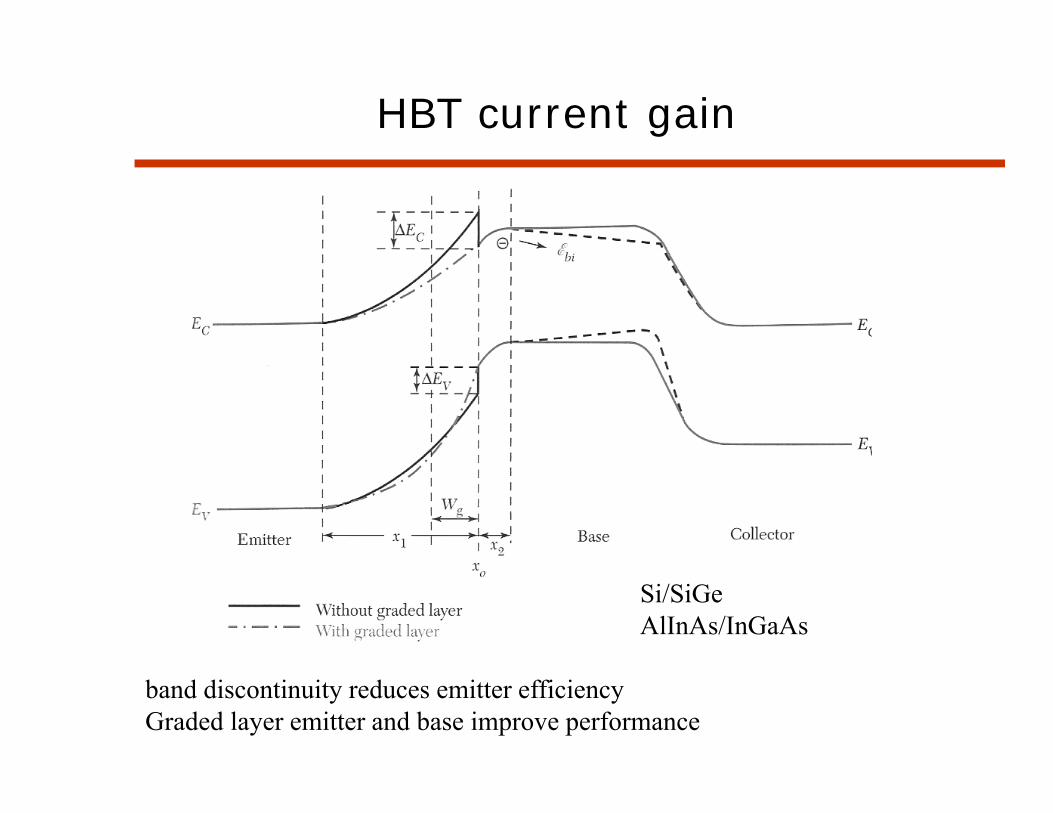
band discontinuity reduces emitter efficiencyGraded layer emitter and base improve performance
Si/SiGeAlInAs/InGaAs
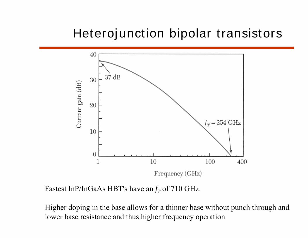
Heterojunction bipolar transistors
Fastest InP/InGaAs HBT's have an fT of 710 GHz.
Higher doping in the base allows for a thinner base without punch through and lower base resistance and thus higher frequency operation
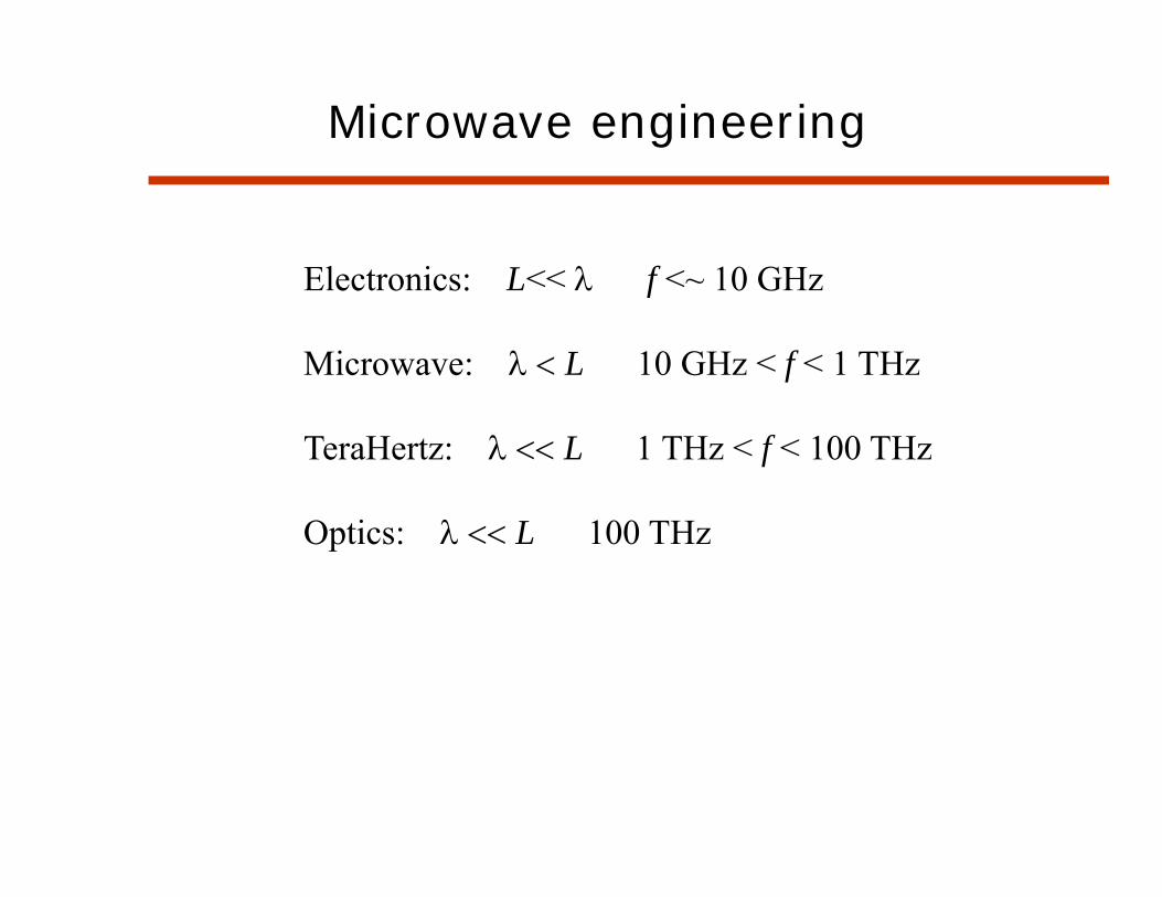
Microwave engineering
Electronics: L<< f <~ 10 GHz
Microwave: L 10 GHz < f < 1 THz
TeraHertz: L 1 THz < f < 100 THz
Optics: L 100 THz
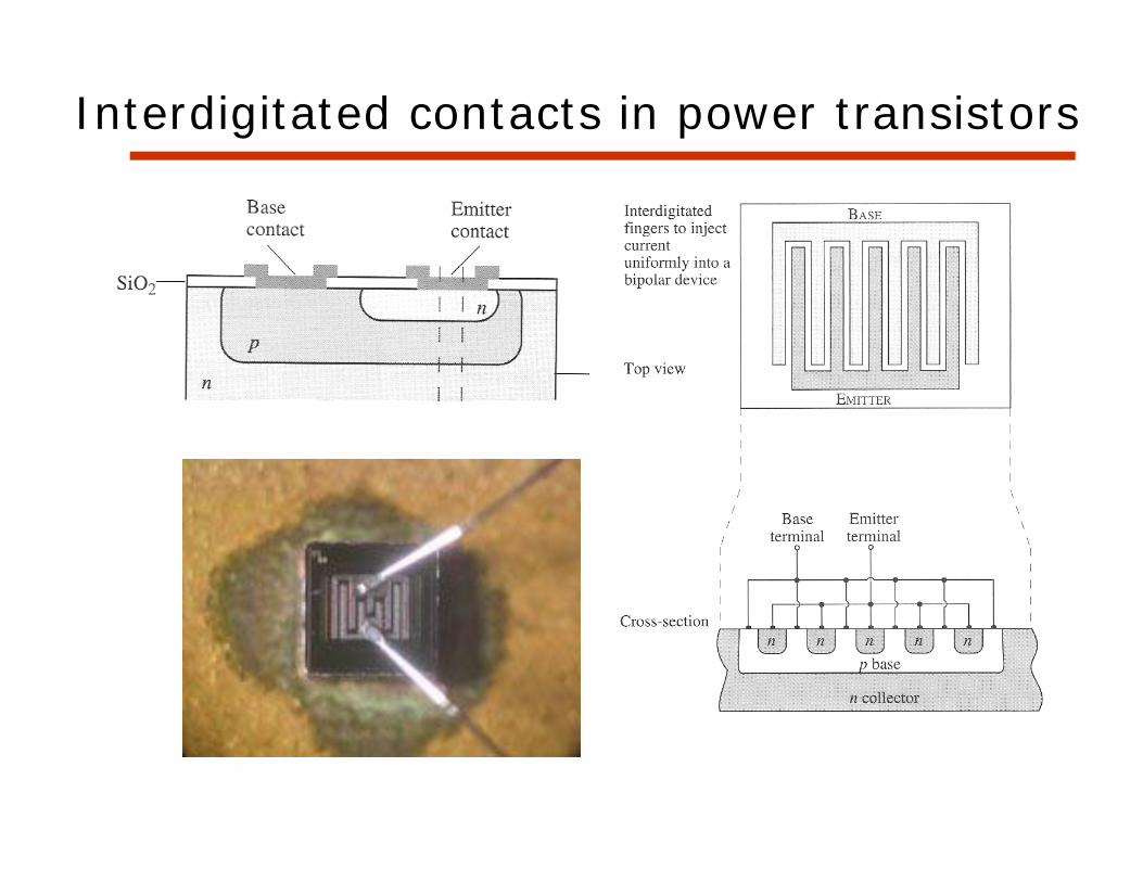
Interdigitated contacts in power transistors
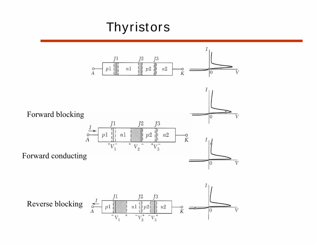
Thyristors
Reverse blocking
Forward blocking
Forward conducting
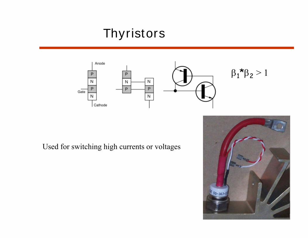
Thyristors
Used for switching high currents or voltages
1*2 > 1
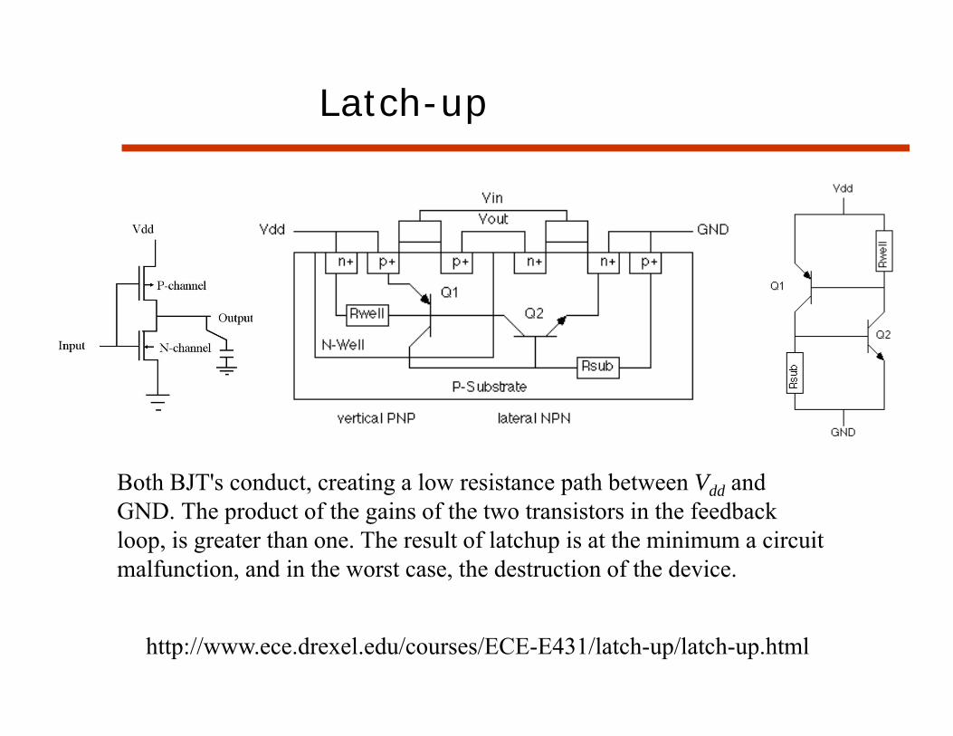
Latch-up
http://www.ece.drexel.edu/courses/ECE-E431/latch-up/latch-up.html
Both BJT's conduct, creating a low resistance path between Vdd and GND. The product of the gains of the two transistors in the feedback loop, is greater than one. The result of latchup is at the minimum a circuit malfunction, and in the worst case, the destruction of the device.
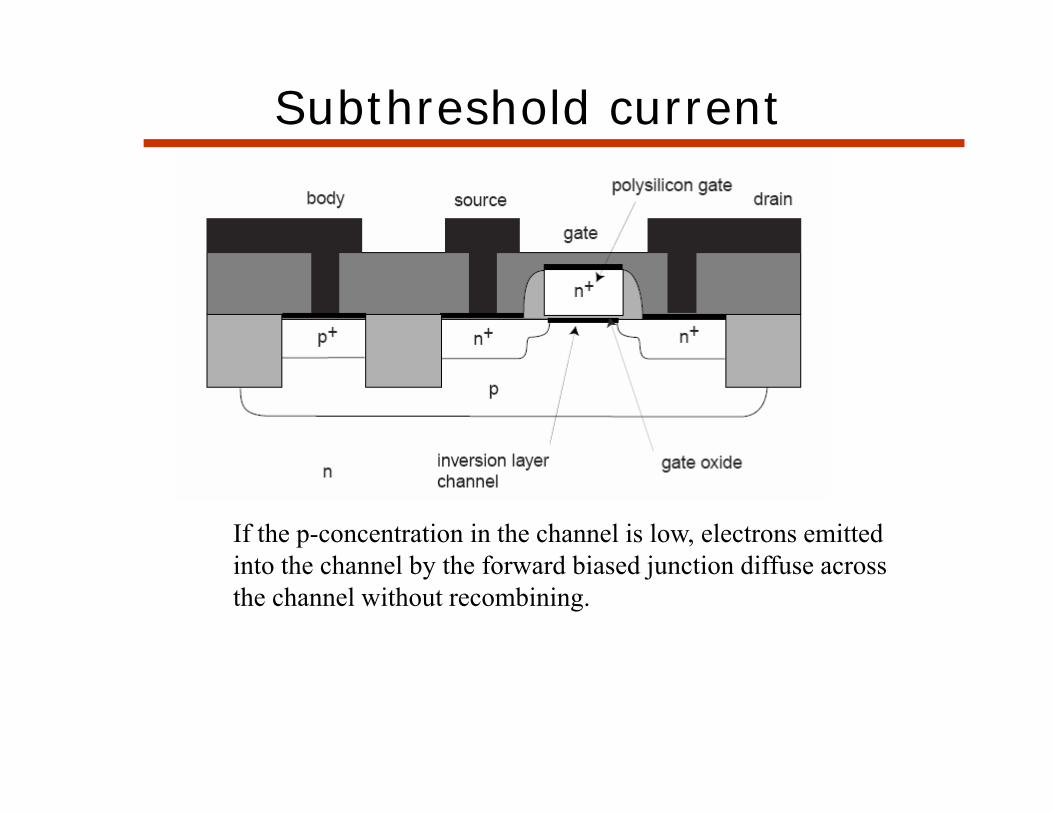
Subthreshold current
If the p-concentration in the channel is low, electrons emitted into the channel by the forward biased junction diffuse across the channel without recombining.