Embed Size (px)
Citation preview
- 1 -
K4S280832O
Rev. 1.0, May. 2010
SAMSUNG ELECTRONICS RESERVES THE RIGHT TO CHANGE PRODUCTS, INFORMATION AND SPECIFICATIONS WITHOUT NOTICE.
Products and specifications discussed herein are for reference purposes only. All information discussed herein is provided on an "AS IS" basis, without warranties of any kind.
This document and all information discussed herein remain the sole and exclusive property of Samsung Electronics. No license of any patent, copyright, mask work, trademark or any other intellectual property right is granted by one party to the other party under this document, by implication, estoppel or other-wise.
Samsung products are not intended for use in life support, critical care, medical, safety equipment, or similar applications where product failure could result in loss of life or personal or physical harm, or any military or defense application, or any governmental procurement to which special terms or provisions may apply.
For updates or additional information about Samsung products, contact your nearest Samsung office.
All brand names, trademarks and registered trademarks belong to their respective owners.
ⓒ 2010 Samsung Electronics Co., Ltd. All rights reserved.
K4S281632O
128Mb O-die SDRAM54TSOP(II) with Lead-Free & Halogen-Free(RoHS compliant)
datasheet
- 2 -
K4S281632O datasheet SDRAMRev. 1.0
K4S280832O
Revision History
Revision No. History Draft Date Remark Editor
1.0 - First Spec. Release May. 2010 - S.H.Kim
- 3 -
K4S281632O datasheet SDRAMRev. 1.0
K4S280832O
Table Of Contents
128Mb O-die SDRAM
1. KEY FEATURES........................................................................................................................................................... 4
2. GENERAL DESCRIPTION ........................................................................................................................................... 4
3. ORDERING INFORMATION ........................................................................................................................................ 4
4. PACKAGE PHYSICAL DIMENSION ............................................................................................................................5
5. FUNCTIONAL BLOCK DIAGRAM ................................................................................................................................ 6
6. PIN CONFIGURATION (TOP VIEW)............................................................................................................................7
7. INPUT/OUTPUT FUNCTION DESCRIPTION ..............................................................................................................7
8. ABSOLUTE MAXIMUM RATINGS ...............................................................................................................................8
9. DC OPERATING CONDITIONS ...................................................................................................................................8
10. CAPACITANCE ..........................................................................................................................................................8
11. DC CHARACTERISTICS (x8)..................................................................................................................................... 9
12. DC CHARACTERISTICS (x16)...................................................................................................................................10
13. AC OPERATING TEST CONDITIONS ....................................................................................................................... 11
14. OPERATING AC PARAMETER ................................................................................................................................. 12
15. AC CHARACTERISTICS ............................................................................................................................................13
16. DQ BUFFER OUTPUT DRIVE CHARACTERISTICS................................................................................................. 13
17. IBIS SPECIFICATION.................................................................................................................................................14
18. SIMPLIFIED TRUTH TABLE ......................................................................................................................................18
- 4 -
K4S281632O datasheet SDRAMRev. 1.0
K4S280832O
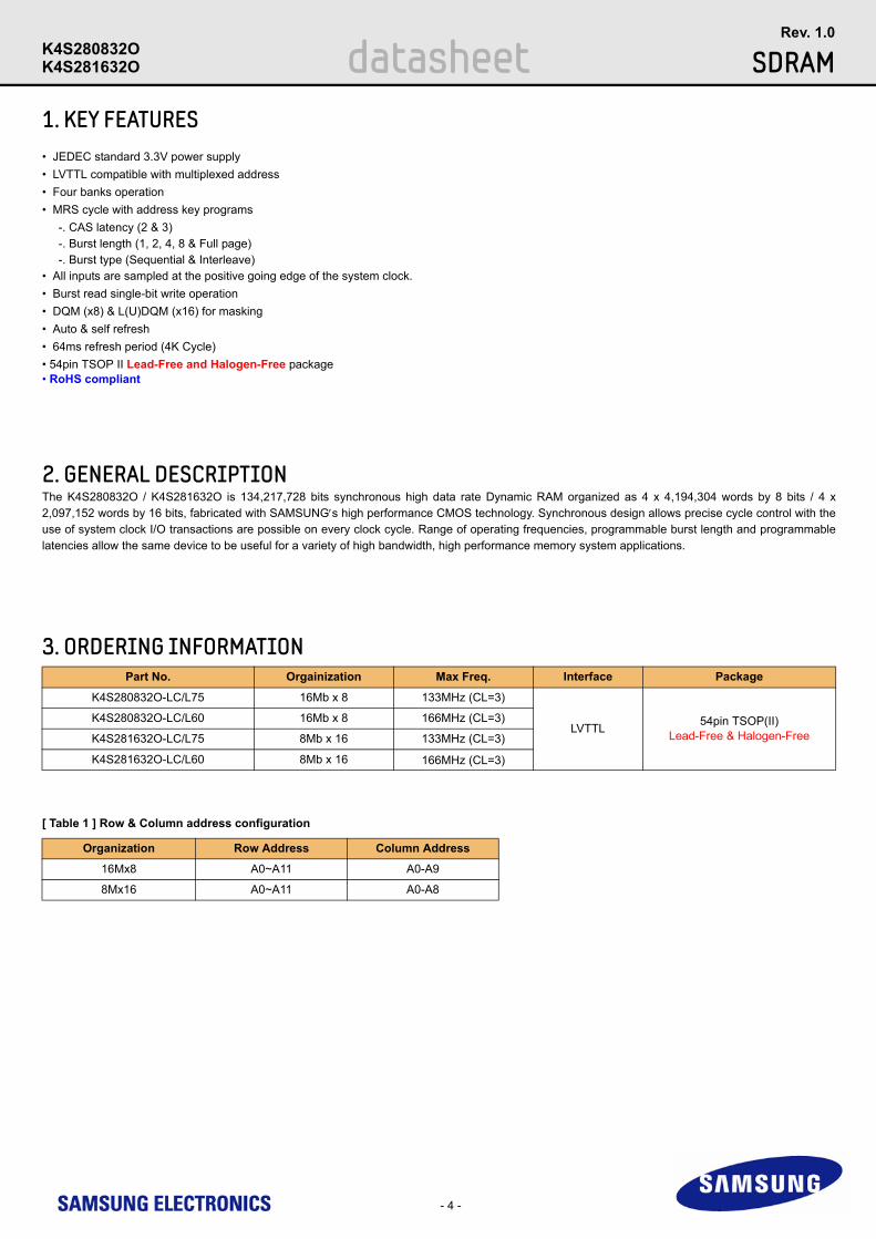
1. KEY FEATURES• JEDEC standard 3.3V power supply• LVTTL compatible with multiplexed address• Four banks operation • MRS cycle with address key programs -. CAS latency (2 & 3) -. Burst length (1, 2, 4, 8 & Full page) -. Burst type (Sequential & Interleave)• All inputs are sampled at the positive going edge of the system clock. • Burst read single-bit write operation• DQM (x8) & L(U)DQM (x16) for masking• Auto & self refresh• 64ms refresh period (4K Cycle)• 54pin TSOP II Lead-Free and Halogen-Free package• RoHS compliant
2. GENERAL DESCRIPTIONThe K4S280832O / K4S281632O is 134,217,728 bits synchronous high data rate Dynamic RAM organized as 4 x 4,194,304 words by 8 bits / 4 x 2,097,152 words by 16 bits, fabricated with SAMSUNG′s high performance CMOS technology. Synchronous design allows precise cycle control with the use of system clock I/O transactions are possible on every clock cycle. Range of operating frequencies, programmable burst length and programmable latencies allow the same device to be useful for a variety of high bandwidth, high performance memory system applications.
3. ORDERING INFORMATION
[ Table 1 ] Row & Column address configuration
Part No. Orgainization Max Freq. Interface Package
K4S280832O-LC/L75 16Mb x 8 133MHz (CL=3)
LVTTL 54pin TSOP(II)Lead-Free & Halogen-Free
K4S280832O-LC/L60 16Mb x 8 166MHz (CL=3)
K4S281632O-LC/L75 8Mb x 16 133MHz (CL=3)
K4S281632O-LC/L60 8Mb x 16 166MHz (CL=3)
Organization Row Address Column Address
16Mx8 A0~A11 A0-A9
8Mx16 A0~A11 A0-A8
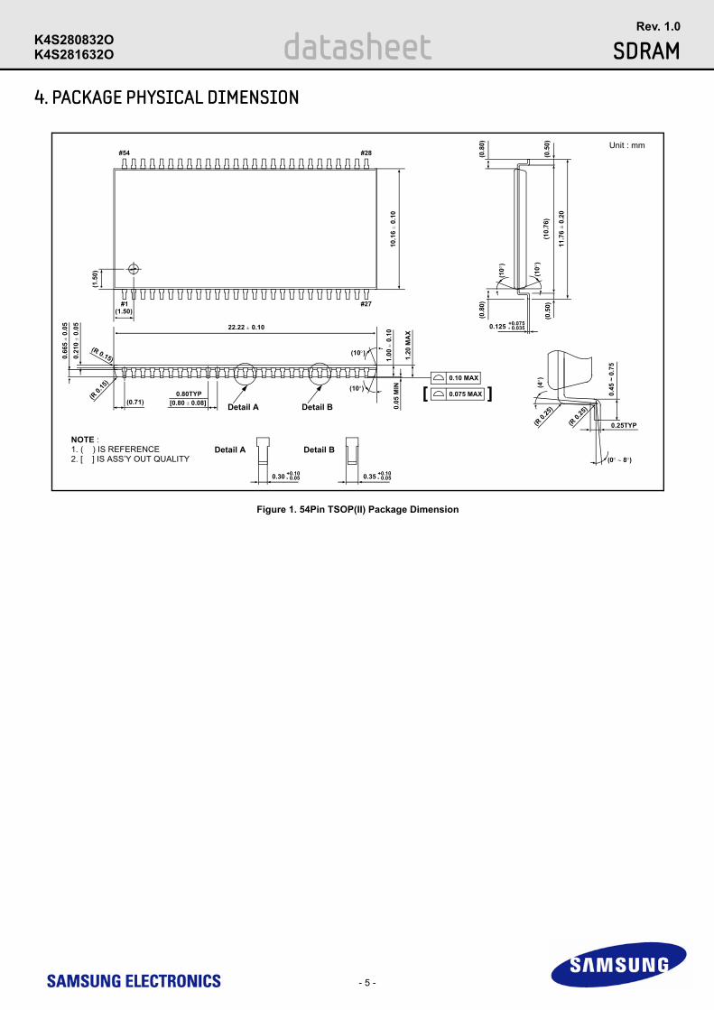
Figure 1. 54Pin TSOP(II) Package Dimension
- 5 -
K4S281632O datasheet SDRAMRev. 1.0
K4S280832O
4. PACKAGE PHYSICAL DIMENSION
#1(1.50)
(1.5
0)
#54 #28
#27
10.1
6 ± 0
.10
(R 0.15)
22.22 ± 0.10
0.21
0 ± 0
.05
0.66
5 ± 0
.05
(R 0.
15)
(0.71) [0.80 ± 0.08]0.80TYP
(10°)
1.00
± 0.
100.
05 M
IN(10°)
1.20
MA
X
0.10 MAX
0.075 MAX[ [
(10.
76)
0.125 +0.075- 0.035
(10°
)
(10°
)
11.7
6 ±
0.20
(0.8
0)(0
.80)
(0.5
0)(4
°)
0.45
~ 0
.75
(0° ∼ 8°)
0.25TYP(R 0.
25)
(R 0.
25)
(0.5
0)
Unit : mm
NOTE :1. ( ) IS REFERENCE2. [ ] IS ASS’Y OUT QUALITY
Detail A
0.30 +0.10- 0.05
Detail B
0.35 +0.10- 0.05
Detail BDetail A
- 6 -
K4S281632O datasheet SDRAMRev. 1.0
K4S280832O
5. FUNCTIONAL BLOCK DIAGRAM
Bank Select
Data Input Register
4M x 8 / 2M x 16
4M x 8 / 2M x 16
Sense AMP
Output B
ufferI/O
Control
Column Decoder
Latency & Burst Length
Programming Register
Address R
egister
Row
BufferR
efresh Counter
Row
Decoder
Col. Buffer
LRA
S
LCB
R
LCKE
LRAS LCBR LWE LDQM
CLK CKE CS RAS CAS WE L(U)DQM
LWE
LDQM
DQi
CLK
ADD
LCAS LWCBR
4M x 8 / 2M x 16
4M x 8 / 2M x 16
Timing Register
* Samsung Electronics reserves the right to change products or specification without notice.
- 7 -
K4S281632O datasheet SDRAMRev. 1.0
K4S280832O
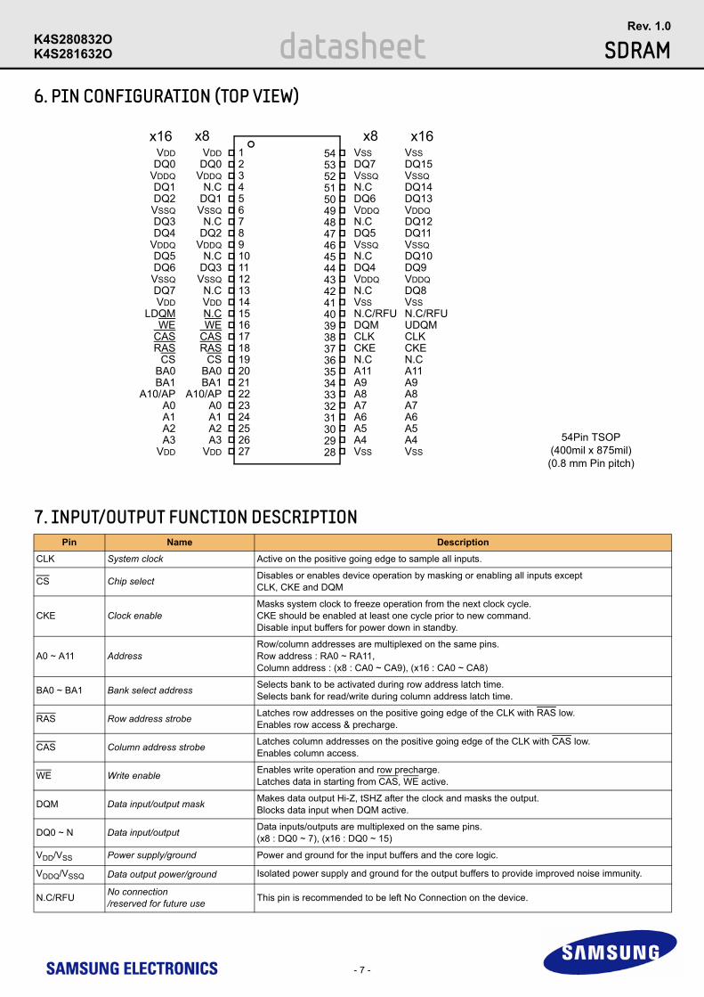
6. PIN CONFIGURATION (TOP VIEW)
7. INPUT/OUTPUT FUNCTION DESCRIPTIONPin Name Description
CLK System clock Active on the positive going edge to sample all inputs.
CS Chip select Disables or enables device operation by masking or enabling all inputs except CLK, CKE and DQM
CKE Clock enableMasks system clock to freeze operation from the next clock cycle.CKE should be enabled at least one cycle prior to new command.Disable input buffers for power down in standby.
A0 ~ A11 AddressRow/column addresses are multiplexed on the same pins.Row address : RA0 ~ RA11, Column address : (x8 : CA0 ~ CA9), (x16 : CA0 ~ CA8)
BA0 ~ BA1 Bank select address Selects bank to be activated during row address latch time.Selects bank for read/write during column address latch time.
RAS Row address strobe Latches row addresses on the positive going edge of the CLK with RAS low.Enables row access & precharge.
CAS Column address strobe Latches column addresses on the positive going edge of the CLK with CAS low.Enables column access.
WE Write enable Enables write operation and row precharge.Latches data in starting from CAS, WE active.
DQM Data input/output mask Makes data output Hi-Z, tSHZ after the clock and masks the output.Blocks data input when DQM active.
DQ0 ~ N Data input/output Data inputs/outputs are multiplexed on the same pins.(x8 : DQ0 ~ 7), (x16 : DQ0 ~ 15)
VDD/VSS Power supply/ground Power and ground for the input buffers and the core logic.
VDDQ/VSSQ Data output power/ground Isolated power supply and ground for the output buffers to provide improved noise immunity.
N.C/RFU No connection/reserved for future use This pin is recommended to be left No Connection on the device.
54Pin TSOP(400mil x 875mil)(0.8 mm Pin pitch)
123456789101112131415161718192021222324252627
545352515049484746454443424140393837363534333231302928
VDDDQ0
VDDQN.C
DQ1VSSQ
N.CDQ2
VDDQN.C
DQ3VSSQ
N.CVDDN.CWE
CASRAS
CSBA0BA1
A10/APA0A1A2A3
VDD
VSSDQ7VSSQN.CDQ6VDDQN.CDQ5VSSQN.CDQ4VDDQN.CVSSN.C/RFUDQMCLKCKEN.CA11A9A8A7A6A5A4VSS
VDDDQ0
VDDQDQ1DQ2VSSQDQ3DQ4
VDDQDQ5DQ6VSSQDQ7VDD
LDQMWE
CASRAS
CSBA0BA1
A10/APA0A1A2A3
VDD
VSSDQ15VSSQDQ14DQ13VDDQDQ12DQ11VSSQDQ10DQ9VDDQDQ8VSSN.C/RFUUDQMCLKCKEN.CA11A9A8A7A6A5A4VSS
x16 x8 x16x8
- 8 -
K4S281632O datasheet SDRAMRev. 1.0
K4S280832O
8. ABSOLUTE MAXIMUM RATINGS
NOTE : Permanent device damage may occur if "ABSOLUTE MAXIMUM RATINGS" are exceeded.Functional operation should be restricted to recommended operating condition.Exposure to higher than recommended voltage for extended periods of time could affect device reliability.
9. DC OPERATING CONDITIONSRecommended operating conditions (Voltage referenced to VSS = 0V, TA = 0 to 70°C)
NOTE :1. VIH (max) = 5.6V AC. The overshoot voltage duration is ≤ 3ns.2. VIL (min) = -2.0V AC. The undershoot voltage duration is ≤ 3ns.3. Any input 0V ≤ VIN ≤ VDDQ. Input leakage currents include Hi-Z output leakage for all bi-directional buffers with Tri-State outputs.
10. CAPACITANCE(VDD = 3.3V, TA = 23°C, f = 1MHz, VREF =1.4V ± 200 mV)
Parameter Symbol Value Unit
Voltage on any pin relative to VSS VIN, VOUT -1.0 ~ 4.6 V
Voltage on VDD supply relative to VSS VDD, VDDQ -1.0 ~ 4.6 V
Storage temperature TSTG -55 ~ +150 °C
Power dissipation PD 1 W
Short circuit current IOS 50 mA
Parameter Symbol Min Typ Max Unit NOTE
Supply voltage VDD, VDDQ 3.0 3.3 3.6 V
Input logic high voltage VIH 2.0 3.0 VDD+0.3 V 1
Input logic low voltage VIL -0.3 0 0.8 V 2
Output logic high voltage VOH 2.4 - - V IOH = -2mA
Output logic low voltage VOL - - 0.4 V IOL = 2mA
Input leakage current ILI -10 - 10 uA 3
Pin Symbol Min Max Unit
Clock CCLK 2.5 3.5 pF
RAS, CAS, WE, CS, CKE, DQM CIN 2.5 3.8 pF
Address CADD 2.5 3.8 pF
(x8 : DQ0 ~ DQ7), (x16 : DQ0 ~ DQ15) COUT 4.0 6.0 pF

- 9 -
K4S281632O datasheet SDRAMRev. 1.0
K4S280832O
11. DC CHARACTERISTICS (x8)(Recommended operating condition unless otherwise noted, TA = 0 to 70°C)
NOTE :1. Measured with outputs open.2. Refresh period is 64ms.3. K4S280832O-LC4. K4S280832O-LL5. Unless otherwise noticed, input swing level is CMOS(VIH/VIL=VDDQ/VSSQ).
Parameter Symbol Test ConditionVersion
Unit NOTE60 75
Operating current(One bank active) ICC1
Burst length = 1 tRC ≥ tRC(min) IO = 0 mA
40 40 mA 1
Precharge standby current in power-down mode
ICC2P CKE ≤ VIL(max), tCC = 10ns 2 2mA
ICC2PS CKE & CLK ≤ VIL(max), tCC = ∞ 2 2
Precharge standby current in non power-down mode
ICC2NCKE ≥ VIH(min), CS ≥ VIH(min), tCC = 10nsInput signals are changed one time during 20ns
15 15mA
ICC2NSCKE ≥ VIH(min), CLK ≤ VIL(max), tCC = ∞Input signals are stable
10 10
Active standby current in power-down mode
ICC3P CKE ≤ VIL(max), tCC = 10ns 5 5mA
ICC3PS CKE & CLK ≤ VIL(max), tCC = ∞ 5 5
Active standby current in non power-down mode(One bank active)
ICC3NCKE ≥ VIH(min), CS ≥ VIH(min), tCC = 10nsInput signals are changed one time during 20ns
25 25 mA
ICC3NSCKE ≥ VIH(min), CLK ≤ VIL(max), tCC = ∞Input signals are stable
20 20 mA
Operating current(Burst mode) ICC4
IO = 0 mA Page burst4Banks ActivatedtCCD = 2CLKs
60 60 mA 1
Refresh current ICC5 tRC ≥ tRC(min) 100 100 mA 2
Self refresh current ICC6 CKE ≤ 0.2VC 2 2 mA 3
L 0.8 0.8 mA 4
- 10 -
K4S281632O datasheet SDRAMRev. 1.0
K4S280832O
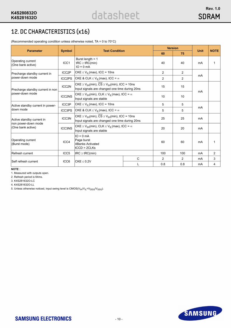
12. DC CHARACTERISTICS (x16)(Recommended operating condition unless otherwise noted, TA = 0 to 70°C)
NOTE :1. Measured with outputs open.2. Refresh period is 64ms.3. K4S281632O-LC4. K4S281632O-LL5. Unless otherwise noticed, input swing level is CMOS(VIH/VIL=VDDQ/VSSQ).
Parameter Symbol Test ConditionVersion
Unit NOTE60 75
Operating current(One bank active) ICC1
Burst length = 1 tRC ≥ tRC(min) IO = 0 mA
40 40 mA 1
Precharge standby current in power-down mode
ICC2P CKE ≤ VIL(max), tCC = 10ns 2 2mA
ICC2PS CKE & CLK ≤ VIL(max), tCC = ∞ 2 2
Precharge standby current in non power-down mode
ICC2NCKE ≥ VIH(min), CS ≥ VIH(min), tCC = 10nsInput signals are changed one time during 20ns
15 15mA
ICC2NSCKE ≥ VIH(min), CLK ≤ VIL(max), tCC = ∞Input signals are stable
10 10
Active standby current in power-down mode
ICC3P CKE ≤ VIL(max), tCC = 10ns 5 5mA
ICC3PS CKE & CLK ≤ VIL(max), tCC = ∞ 5 5
Active standby current in non power-down mode(One bank active)
ICC3NCKE ≥ VIH(min), CS ≥ VIH(min), tCC = 10nsInput signals are changed one time during 20ns
25 25 mA
ICC3NSCKE ≥ VIH(min), CLK ≤ VIL(max), tCC = ∞Input signals are stable
20 20 mA
Operating current(Burst mode) ICC4
IO = 0 mA Page burst4Banks ActivatedtCCD = 2CLKs
60 60 mA 1
Refresh current ICC5 tRC ≥ tRC(min) 100 100 mA 2
Self refresh current ICC6 CKE ≤ 0.2VC 2 2 mA 3
L 0.8 0.8 mA 4
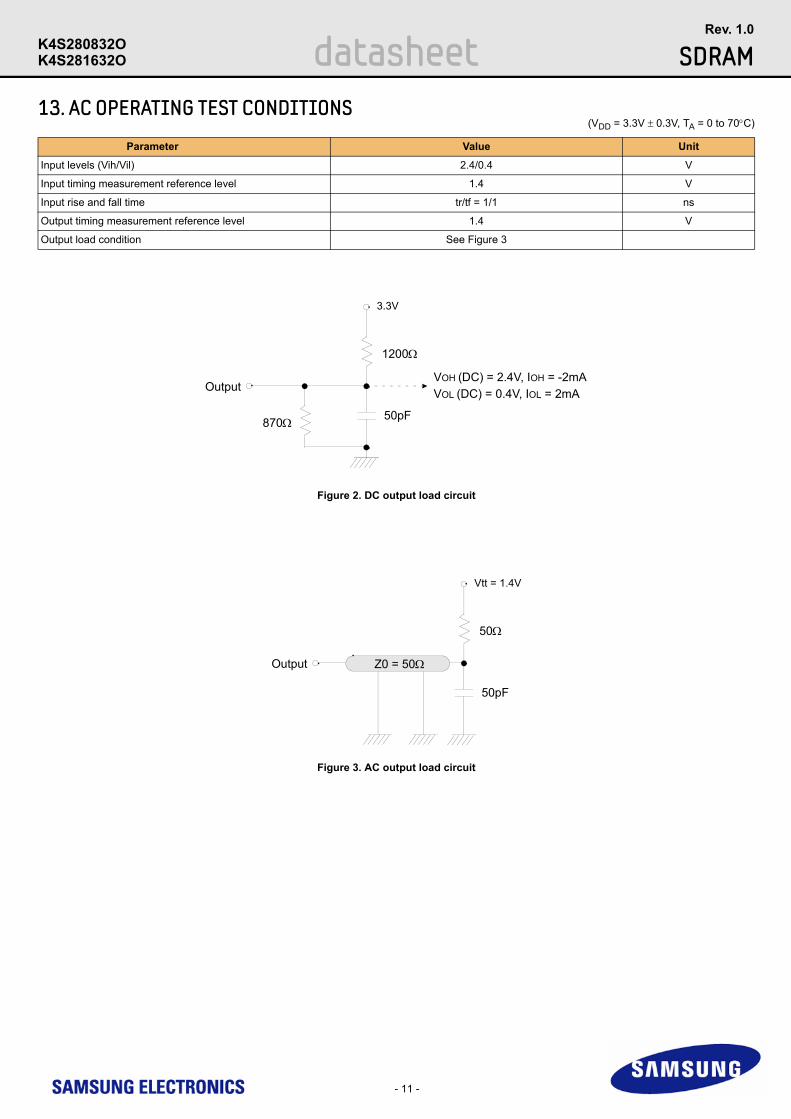
Figure 3. AC output load circuit
Figure 2. DC output load circuit
- 11 -
K4S281632O datasheet SDRAMRev. 1.0
K4S280832O
13. AC OPERATING TEST CONDITIONS (VDD = 3.3V ± 0.3V, TA = 0 to 70°C)
Parameter Value Unit
Input levels (Vih/Vil) 2.4/0.4 V
Input timing measurement reference level 1.4 V
Input rise and fall time tr/tf = 1/1 ns
Output timing measurement reference level 1.4 V
Output load condition See Figure 3
3.3V
1200Ω
870Ω
Output
50pF
VOH (DC) = 2.4V, IOH = -2mAVOL (DC) = 0.4V, IOL = 2mA
Vtt = 1.4V
50Ω
Output
50pF
Z0 = 50Ω
- 12 -
K4S281632O datasheet SDRAMRev. 1.0
K4S280832O
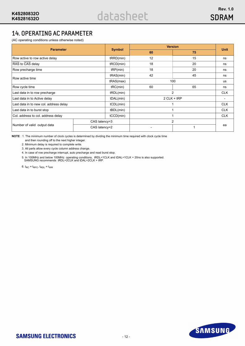
14. OPERATING AC PARAMETER(AC operating conditions unless otherwise noted)
NOTE : 1. The minimum number of clock cycles is determined by dividing the minimum time required with clock cycle time and then rounding off to the next higher integer.2. Minimum delay is required to complete write.3. All parts allow every cycle column address change.4. In case of row precharge interrupt, auto precharge and read burst stop.
5. In 100MHz and below 100MHz operating conditions, tRDL=1CLK and tDAL=1CLK + 20ns is also supported. SAMSUNG recommends tRDL=2CLK and tDAL=2CLK + tRP.
6. tRC = tRFC, tRDL = tWR
Parameter SymbolVersion
Unit60 75
Row active to row active delay tRRD(min) 12 15 ns
RAS to CAS delay tRCD(min) 18 20 ns
Row precharge time tRP(min) 18 20 ns
Row active timetRAS(min) 42 45 ns
tRAS(max) 100 us
Row cycle time tRC(min) 60 65 ns
Last data in to row precharge tRDL(min) 2 CLK
Last data in to Active delay tDAL(min) 2 CLK + tRP -
Last data in to new col. address delay tCDL(min) 1 CLK
Last data in to burst stop tBDL(min) 1 CLK
Col. address to col. address delay tCCD(min) 1 CLK
Number of valid output dataCAS latency=3 2
eaCAS latency=2 - 1
- 13 -
K4S281632O datasheet SDRAMRev. 1.0
K4S280832O
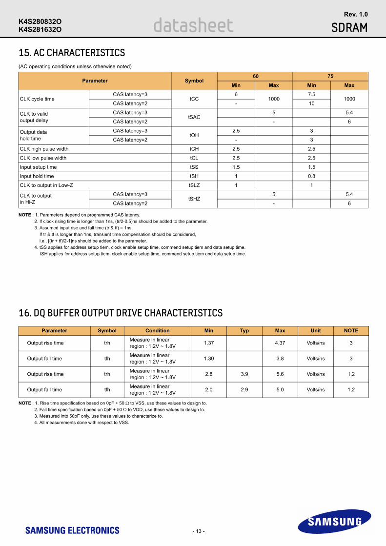
15. AC CHARACTERISTICS(AC operating conditions unless otherwise noted)
NOTE : 1. Parameters depend on programmed CAS latency.2. If clock rising time is longer than 1ns, (tr/2-0.5)ns should be added to the parameter.3. Assumed input rise and fall time (tr & tf) = 1ns. If tr & tf is longer than 1ns, transient time compensation should be considered, i.e., [(tr + tf)/2-1]ns should be added to the parameter.4. tSS applies for address setup tiem, clock enable setup time, commend setup tiem and data setup time.
tSH applies for address setup tiem, clock enable setup time, commend setup tiem and data setup time.
16. DQ BUFFER OUTPUT DRIVE CHARACTERISTICS
NOTE : 1. Rise time specification based on 0pF + 50 Ω to VSS, use these values to design to.2. Fall time specification based on 0pF + 50 Ω to VDD, use these values to design to.3. Measured into 50pF only, use these values to characterize to.4. All measurements done with respect to VSS.
Parameter Symbol 60 75
Min Max Min Max
CLK cycle timeCAS latency=3
tCC6
10007.5
1000CAS latency=2 - 10
CLK to validoutput delay
CAS latency=3tSAC
5 5.4
CAS latency=2 - 6
Output datahold time
CAS latency=3tOH
2.5 3
CAS latency=2 - 3
CLK high pulse width tCH 2.5 2.5
CLK low pulse width tCL 2.5 2.5
Input setup time tSS 1.5 1.5
Input hold time tSH 1 0.8
CLK to output in Low-Z tSLZ 1 1
CLK to output in Hi-Z
CAS latency=3tSHZ
5 5.4
CAS latency=2 - 6
Parameter Symbol Condition Min Typ Max Unit NOTE
Output rise time trh Measure in linear region : 1.2V ~ 1.8V 1.37 4.37 Volts/ns 3
Output fall time tfh Measure in linear region : 1.2V ~ 1.8V 1.30 3.8 Volts/ns 3
Output rise time trh Measure in linear region : 1.2V ~ 1.8V 2.8 3.9 5.6 Volts/ns 1,2
Output fall time tfh Measure in linear region : 1.2V ~ 1.8V 2.0 2.9 5.0 Volts/ns 1,2
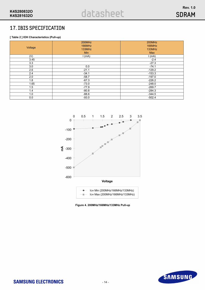
Figure 4. 200MHz/166MHz/133MHz Pull-up
- 14 -
K4S281632O datasheet SDRAMRev. 1.0
K4S280832O
17. IBIS SPECIFICATION[ Table 2 ] IOH Characteristics (Pull-up)
Voltage
200MHz166MHz133MHz
Min
200MHz166MHz133MHz
Max(V) I (mA) I (mA)
3.45 -2.43.3 -27.33.0 0.0 -74.12.6 -21.1 -129.22.4 -34.1 -153.32.0 -58.7 -197.01.8 -67.3 -226.2
1.65 -73.0 -248.01.5 -77.9 -269.71.4 -80.8 -284.31.0 -88.6 -344.50.0 -93.0 -502.4
0
-100
-200
-300
-400
-500
-600
0 30.5 1 1.5 2 2.5 3.5
Voltage
mA
IOH Min (200MHz/166MHz/133MHz)IOH Max (200MHz/166MHz/133MHz)
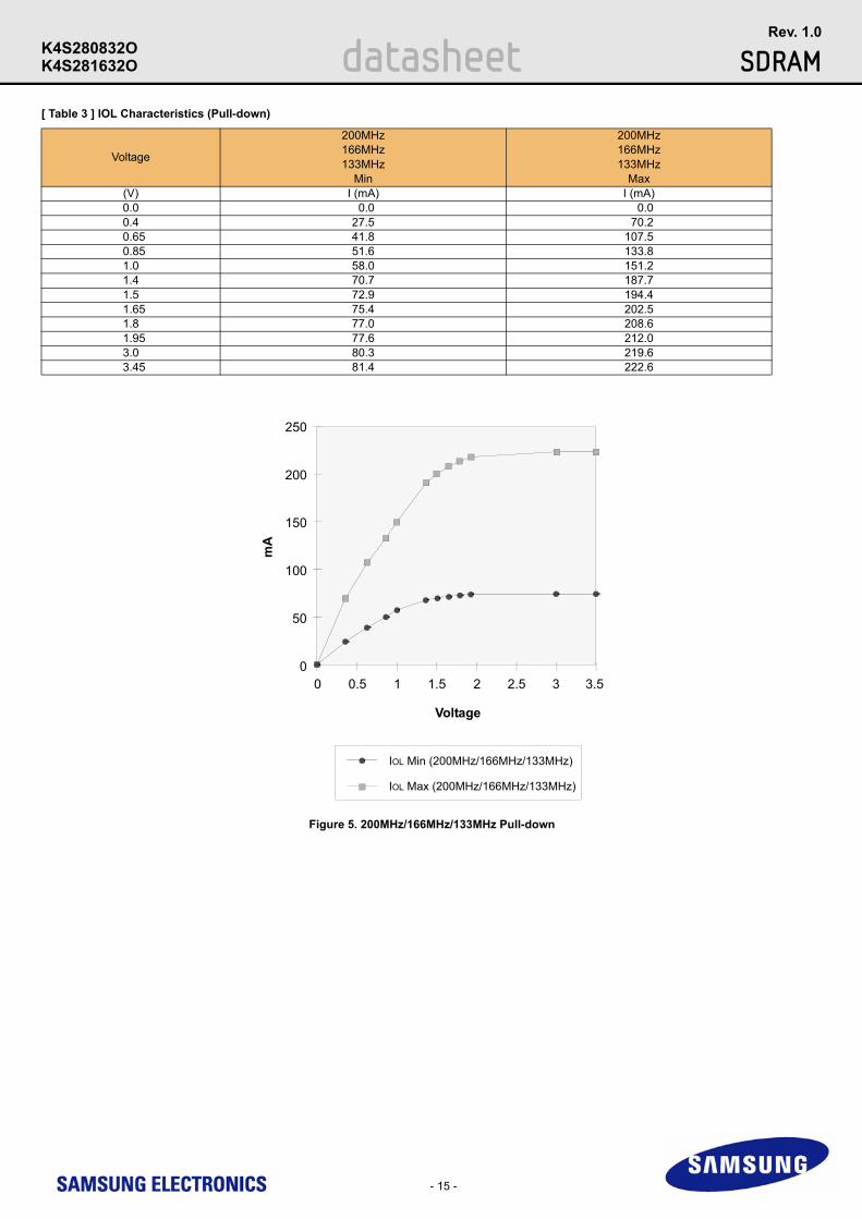
Figure 5. 200MHz/166MHz/133MHz Pull-down
- 15 -
K4S281632O datasheet SDRAMRev. 1.0
K4S280832O
[ Table 3 ] IOL Characteristics (Pull-down)
Voltage
200MHz166MHz133MHz
Min
200MHz166MHz133MHz
Max(V) I (mA) I (mA)0.0 0.0 0.00.4 27.5 70.2
0.65 41.8 107.5 0.85 51.6 133.8
1.0 58.0 151.21.4 70.7 187.71.5 72.9 194.4
1.65 75.4 202.51.8 77.0 208.6
1.95 77.6 212.03.0 80.3 219.6
3.45 81.4 222.6
250
200
150
100
50
00 30.5 1 1.5 2 2.5 3.5
Voltage
mA
IOL Min (200MHz/166MHz/133MHz)
IOL Max (200MHz/166MHz/133MHz)

Figure 6. Minimum VDD clamp current (Referenced to VDD)
- 16 -
K4S281632O datasheet SDRAMRev. 1.0
K4S280832O
[ Table 4 ] VDD Clamp @ CLK, CKE, CS, DQM & DQ
VDD (V) I (mA)0.0 0.00.2 0.00.4 0.00.6 0.00.7 0.00.8 0.00.9 0.01.0 0.231.2 1.341.4 3.021.6 5.061.8 7.352.0 9.832.2 12.482.4 15.302.6 18.31
20
15
10
5
00 31 2
Voltage
mA
I (mA)
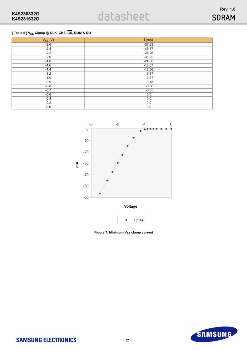
Figure 7. Minimum VSS clamp current
- 17 -
K4S281632O datasheet SDRAMRev. 1.0
K4S280832O
[ Table 5 ] VSS Clamp @ CLK, CKE, CS, DQM & DQ
VSS (V) I (mA)-2.6 -57.23-2.4 -45.77-2.2 -38.26-2.0 -31.22-1.8 -24.58-1.6 -18.37-1.4 -12.56-1.2 -7.57-1.0 -3.37-0.9 -1.75-0.8 -0.58-0.7 -0.05-0.6 0.0-0.4 0.0-0.2 0.0 0.0 0.0
mA
I (mA)
0
-10
-20
-30
-40
-3 0-2 -1
-50
-60
Voltage
- 18 -
K4S281632O datasheet SDRAMRev. 1.0
K4S280832O
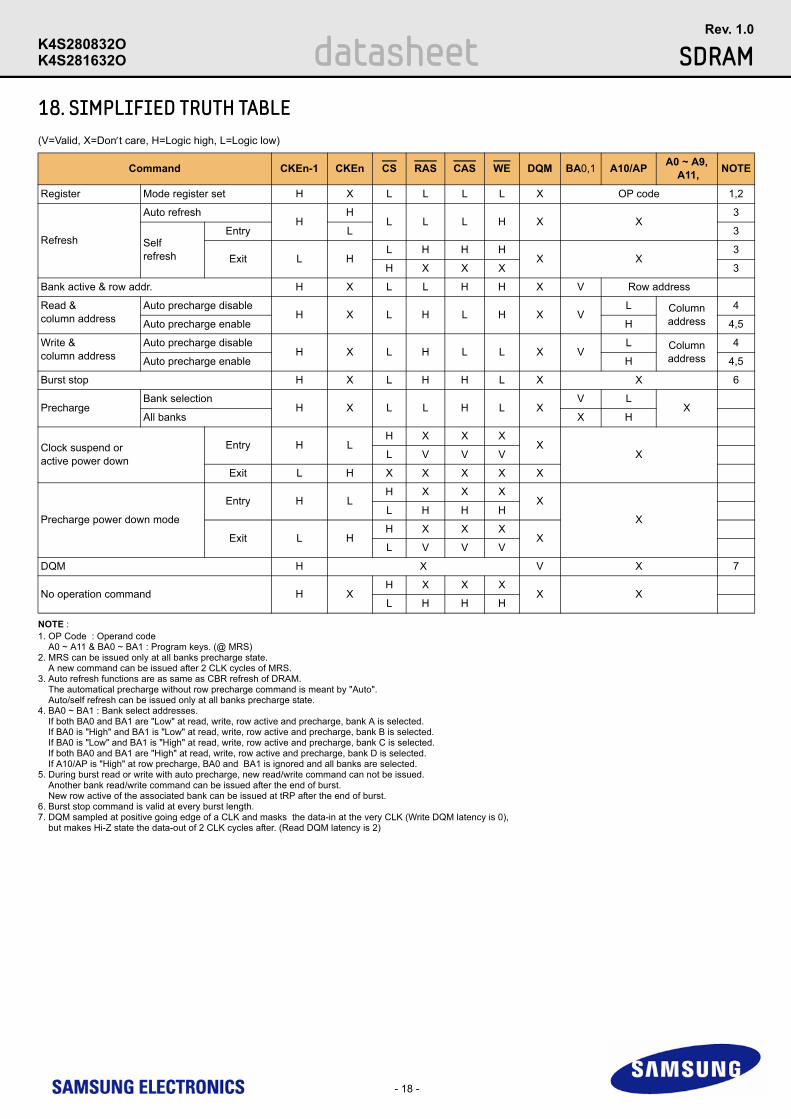
18. SIMPLIFIED TRUTH TABLE(V=Valid, X=Don′t care, H=Logic high, L=Logic low)
NOTE :1. OP Code : Operand code A0 ~ A11 & BA0 ~ BA1 : Program keys. (@ MRS)2. MRS can be issued only at all banks precharge state. A new command can be issued after 2 CLK cycles of MRS.3. Auto refresh functions are as same as CBR refresh of DRAM. The automatical precharge without row precharge command is meant by "Auto". Auto/self refresh can be issued only at all banks precharge state.4. BA0 ~ BA1 : Bank select addresses. If both BA0 and BA1 are "Low" at read, write, row active and precharge, bank A is selected. If BA0 is "High" and BA1 is "Low" at read, write, row active and precharge, bank B is selected. If BA0 is "Low" and BA1 is "High" at read, write, row active and precharge, bank C is selected. If both BA0 and BA1 are "High" at read, write, row active and precharge, bank D is selected. If A10/AP is "High" at row precharge, BA0 and BA1 is ignored and all banks are selected.5. During burst read or write with auto precharge, new read/write command can not be issued. Another bank read/write command can be issued after the end of burst. New row active of the associated bank can be issued at tRP after the end of burst.6. Burst stop command is valid at every burst length.7. DQM sampled at positive going edge of a CLK and masks the data-in at the very CLK (Write DQM latency is 0), but makes Hi-Z state the data-out of 2 CLK cycles after. (Read DQM latency is 2)
Command CKEn-1 CKEn CS RAS CAS WE DQM BA0,1 A10/AP A0 ~ A9, A11, NOTE
Register Mode register set H X L L L L X OP code 1,2
Refresh
Auto refreshH
HL L L H X X
3
Self refresh
Entry L 3
Exit L HL H H H
X X3
H X X X 3
Bank active & row addr. H X L L H H X V Row address
Read &column address
Auto precharge disableH X L H L H X V
L Columnaddress
4
Auto precharge enable H 4,5
Write &column address
Auto precharge disableH X L H L L X V
L Columnaddress
4
Auto precharge enable H 4,5
Burst stop H X L H H L X X 6
PrechargeBank selection
H X L L H L XV L
XAll banks X H
Clock suspend oractive power down
Entry H LH X X X
XXL V V V
Exit L H X X X X X
Precharge power down mode
Entry H LH X X X
X
XL H H H
Exit L HH X X X
XL V V V
DQM H X V X 7
No operation command H XH X X X
X XL H H H
![4Gb A-die DDR3 SDRAM - МТ System · DDR3 SDRAM Addressing ... 11. 4Gb DDR3 SDRAM A-die IDD Specification Table ... [ Table 1 ] Samsung 4Gb DDR3 A-die ordering information table](https://img.pdfslide.us/doc/110x75/5ad5dbf67f8b9a5c638d9a55/4gb-a-die-ddr3-sdram-sdram-addressing-11-4gb-ddr3-sdram-a-die-idd-specification.jpg)
![4Gb E-die DDR3 SDRAM x16 - samsung.com · - 5 - K4B4G1646E datasheet DDR3 SDRAM Rev. 1.01 1. Ordering Information [ Table 1 ] Samsung 4Gb DDR3 E-die ordering information table NOTE:](https://img.pdfslide.us/doc/110x75/5e15e846c6296e58e6146f8b/4gb-e-die-ddr3-sdram-x16-5-k4b4g1646e-datasheet-ddr3-sdram-rev-101-1-ordering.jpg)
![4Gb D-die DDR3 SDRAM- 5 - K4B4G0846D datasheet DDR3 SDRAM Rev. 1.23 K4B4G0446D 1. Ordering Information [ Table 1 ] Samsung 4Gb DDR3 D-die ordering information table NOTE: 1. Speed](https://img.pdfslide.us/doc/110x75/5e73e86eb6f1e10b075d492a/4gb-d-die-ddr3-sdram-5-k4b4g0846d-datasheet-ddr3-sdram-rev-123-k4b4g0446d.jpg)
![1Gb F-die DDR3 SDRAM...- 5 - K4B1G0846F datasheet DDR3 SDRAM Rev. 1.21 K4B1G0446F 1. Ordering Information [ Table 1 ] Samsung 1Gb DDR3 F-die ordering information table NOTE: 1. Speed](https://img.pdfslide.us/doc/110x75/6118fdb29861ea1e5e6a2225/1gb-f-die-ddr3-5-k4b1g0846f-datasheet-ddr3-sdram-rev-121-k4b1g0446f-1.jpg)
![2Gb C-die DDR3 SDRAM Industrial€¦ · datasheet DDR3 SDRAM Rev. 1.0 K4B2G1646C Industrial 1. Ordering Information [ Table 1 ] Samsung 2Gb DDR3 C-die ordering information table NOTE:](https://img.pdfslide.us/doc/110x75/5ecc8b7cc35ff9103a633f0f/2gb-c-die-ddr3-sdram-datasheet-ddr3-sdram-rev-10-k4b2g1646c-industrial-1-ordering.jpg)
![4Gb E-die DDR3L SDRAM Only x16...- 5 - K4B4G1646E datasheet DDR3L SDRAM Rev. 1.1 1. Ordering Information [ Table 1 ] Samsung 4Gb DDR3L E-die ordering information table NOTE: 1. Speed](https://img.pdfslide.us/doc/110x75/5e61d9961906103bcb7627ba/4gb-e-die-ddr3l-sdram-only-x16-5-k4b4g1646e-datasheet-ddr3l-sdram-rev-11.jpg)


![8Gb C-die DDR4 SDRAM - Amazon S3 · - 5 - K4A8G085WC datasheet DDR4 SDRAM K4A8G045WC Rev. 1.31 1. Ordering Information [ Table 1 ] Samsung 8Gb DDR4 C-die Ordering Information Table](https://img.pdfslide.us/doc/110x75/5e7d528f729206196d614aad/8gb-c-die-ddr4-sdram-amazon-s3-5-k4a8g085wc-datasheet-ddr4-sdram-k4a8g045wc.jpg)
![4Gb D-die DDR3L SDRAM - Samsung US | Mobile | TV...- 5 - K4B4G0846D datasheet DDR3L SDRAM Rev. 1.3 K4B4G0446D 1. Ordering Information [ Table 1 ] Samsung 4Gb DDR3L D-die ordering information](https://img.pdfslide.us/doc/110x75/5fe2bb5ed9f5085cb36d4a6d/4gb-d-die-ddr3l-sdram-samsung-us-mobile-tv-5-k4b4g0846d-datasheet.jpg)