Embed Size (px)
Citation preview

128Mb: 8 Meg x 16 Async/Page/Burst CellularRAM 1.5 Async/Page/Burst CellularRAM 1.5 Memory
Async/Page/Burst CellularRAMTM 1.5MT45W8MW16BGX
Features• Single device supports asynchronous, page, and
burst operations• VCC, VCCQ voltages
– 1.70–1.95V VCC – 1.7–3.6V1 VCCQ
• Random access time: 70ns• Burst mode READ and WRITE access
– 4, 8, 16, or 32 words, or continuous burst– Burst wrap or sequential– MAX clock rate: 133 MHz (tCLK = 7.5ns)– Burst initial latency: 35ns (5 clocks) at 133 MHz– tACLK: 5.5ns at 133 MHz
• Page mode READ access– Sixteen-word page size– Interpage READ access: 70ns– Intrapage READ access: 20ns
• Low power consumption– Asynchronous READ: <25mA– Intrapage READ: <15mA– Initial access, burst READ:
(37.5ns [5 clocks] at 133 MHz) <45mA– Continuous burst READ: <40mA– Standby: <50µA (TYP at 25°C)– Deep power-down: <3µA (TYP)
• Low-power features– On-chip temperature-compensated refresh (TCR)– Partial-array refresh (PAR)– Deep power-down (DPD) mode
Options Designator
• Configuration– 8 Meg x 16 MT45W8MW16B– VCC core voltage: 1.70–1.95V– VCCQ I/O voltage: 1.7–3.6V1
• Package– 54-ball VFBGA—“green” GX
• Timing– 70ns access –70 – 85ns access –85
Products and specifications discussed herein are
PDF: 09005aef80ec6f79/Source: 09005aef80ec6f65128mb_burst_cr1_5_p26z__1.fm - Rev. H 9/07 EN 1
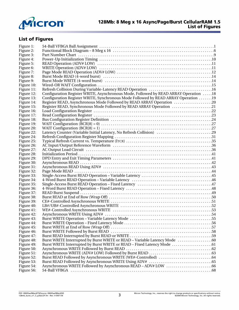
Figure 1: 54-Ball VFBGA Ball Assignment
Notes: 1. The 3.6V I/O and the 133MHz clock fre-quency exceed the CellularRAM 1.5 Work-group specification.
Part Number Example:
MT45W8MW16BGX-7013LWT
Options (continued) Designator
• Frequency– 66 MHz 6– 80 MHz 8– 104 MHz 1– 133 MHz 13
• Standby power at 85°C– Standard: 200µA (MAX) None– Low power: 160µA (MAX) L
• Operating temperature range– Wireless (–30°C to +85°C) WT– Industrial (–40°C to +85°C) IT
A
B
C
D
E
F
G
H
J
1 2 3 4 5 6
Top View(Ball Down)
LB#
DQ8
DQ9
VSSQ
VCCQ
DQ14
DQ15
A18
WAIT
OE#
UB#
DQ10
DQ11
DQ12
DQ13
A19
A8
CLK
A0
A3
A5
A17
A21
A14
A12
A9
ADV#
A2
CE#
DQ1
DQ3
DQ4
DQ5
WE#
A11
RFU
CRE
DQ0
DQ2
VCC
VSS
DQ6
DQ7
A20
RFU
A1
A4
A6
A7
A16
A15
A13
A10
A22
subject to change by Micron without notice.
Micron Technology, Inc., reserves the right to change products or specifications without notice.©2004 Micron Technology, Inc. All rights reserved.

PDF: 09005aef80ec6f79/Source: 09005aef80ec6f65 Micron Technology, Inc., reserves the right to change products or specifications without notice.128mb_burst_cr1_5_p26zTOC.fm - Rev. H 9/07 EN 2 ©2004 Micron Technology, Inc. All rights reserved.
128Mb: 8 Meg x 16 Async/Page/Burst CellularRAM 1.5Table of Contents
Table of Contents Features . . . . . . . . . . . . . . . . . . . . . . . . . . . . . . . . . . . . . . . . . . . . . . . . . . . . . . . . . . . . . . . . . . . . . . . . . . . . . . . . . . . . . . . . . . . . . .1General Description . . . . . . . . . . . . . . . . . . . . . . . . . . . . . . . . . . . . . . . . . . . . . . . . . . . . . . . . . . . . . . . . . . . . . . . . . . . . . . . . . . .5Part-Numbering Information. . . . . . . . . . . . . . . . . . . . . . . . . . . . . . . . . . . . . . . . . . . . . . . . . . . . . . . . . . . . . . . . . . . . . . . . . . .9Functional Description . . . . . . . . . . . . . . . . . . . . . . . . . . . . . . . . . . . . . . . . . . . . . . . . . . . . . . . . . . . . . . . . . . . . . . . . . . . . . . .10
Power-Up Initialization . . . . . . . . . . . . . . . . . . . . . . . . . . . . . . . . . . . . . . . . . . . . . . . . . . . . . . . . . . . . . . . . . . . . . . . . . . . .10Bus Operating Modes . . . . . . . . . . . . . . . . . . . . . . . . . . . . . . . . . . . . . . . . . . . . . . . . . . . . . . . . . . . . . . . . . . . . . . . . . . . . . . . . .10
Asynchronous Mode . . . . . . . . . . . . . . . . . . . . . . . . . . . . . . . . . . . . . . . . . . . . . . . . . . . . . . . . . . . . . . . . . . . . . . . . . . . . . . .10Page Mode READ Operation . . . . . . . . . . . . . . . . . . . . . . . . . . . . . . . . . . . . . . . . . . . . . . . . . . . . . . . . . . . . . . . . . . . . . . . .12Burst Mode Operation. . . . . . . . . . . . . . . . . . . . . . . . . . . . . . . . . . . . . . . . . . . . . . . . . . . . . . . . . . . . . . . . . . . . . . . . . . . . . .13Mixed-Mode Operation . . . . . . . . . . . . . . . . . . . . . . . . . . . . . . . . . . . . . . . . . . . . . . . . . . . . . . . . . . . . . . . . . . . . . . . . . . . .15WAIT Operation . . . . . . . . . . . . . . . . . . . . . . . . . . . . . . . . . . . . . . . . . . . . . . . . . . . . . . . . . . . . . . . . . . . . . . . . . . . . . . . . . . .15LB#/UB# Operation . . . . . . . . . . . . . . . . . . . . . . . . . . . . . . . . . . . . . . . . . . . . . . . . . . . . . . . . . . . . . . . . . . . . . . . . . . . . . . . .16
Low-Power Operation . . . . . . . . . . . . . . . . . . . . . . . . . . . . . . . . . . . . . . . . . . . . . . . . . . . . . . . . . . . . . . . . . . . . . . . . . . . . . . . .17Standby Mode . . . . . . . . . . . . . . . . . . . . . . . . . . . . . . . . . . . . . . . . . . . . . . . . . . . . . . . . . . . . . . . . . . . . . . . . . . . . . . . . . . . . .17Temperature-Compensated Refresh (TCR) . . . . . . . . . . . . . . . . . . . . . . . . . . . . . . . . . . . . . . . . . . . . . . . . . . . . . . . . . . .17Partial-Array Refresh (PAR) . . . . . . . . . . . . . . . . . . . . . . . . . . . . . . . . . . . . . . . . . . . . . . . . . . . . . . . . . . . . . . . . . . . . . . . . .17Deep Power-Down Mode (DPD). . . . . . . . . . . . . . . . . . . . . . . . . . . . . . . . . . . . . . . . . . . . . . . . . . . . . . . . . . . . . . . . . . . . .17
Registers . . . . . . . . . . . . . . . . . . . . . . . . . . . . . . . . . . . . . . . . . . . . . . . . . . . . . . . . . . . . . . . . . . . . . . . . . . . . . . . . . . . . . . . . . . . .17Access Using CRE . . . . . . . . . . . . . . . . . . . . . . . . . . . . . . . . . . . . . . . . . . . . . . . . . . . . . . . . . . . . . . . . . . . . . . . . . . . . . . . . . .18Software Access. . . . . . . . . . . . . . . . . . . . . . . . . . . . . . . . . . . . . . . . . . . . . . . . . . . . . . . . . . . . . . . . . . . . . . . . . . . . . . . . . . . .22Bus Configuration Register (BCR). . . . . . . . . . . . . . . . . . . . . . . . . . . . . . . . . . . . . . . . . . . . . . . . . . . . . . . . . . . . . . . . . . . .24
Burst Length (BCR[2:0]) Default = Continuous Burst . . . . . . . . . . . . . . . . . . . . . . . . . . . . . . . . . . . . . . . . . . . . . . . .25Burst Wrap (BCR[3]) Default = No Wrap . . . . . . . . . . . . . . . . . . . . . . . . . . . . . . . . . . . . . . . . . . . . . . . . . . . . . . . . . . .25Drive Strength (BCR[5:4]) Default = Outputs Use Half-Drive Strength . . . . . . . . . . . . . . . . . . . . . . . . . . . . . . . . .26WAIT Configuration (BCR[8]) Default = WAIT Transitions One Clock Before Data Valid/Invalid . . . . . . . . .27WAIT Polarity (BCR[10]) Default = WAIT Active HIGH . . . . . . . . . . . . . . . . . . . . . . . . . . . . . . . . . . . . . . . . . . . . . . .27Latency Counter (BCR[13:11]) Default = Three Clock Latency . . . . . . . . . . . . . . . . . . . . . . . . . . . . . . . . . . . . . . . .28Initial Access Latency (BCR[14]) Default = Variable . . . . . . . . . . . . . . . . . . . . . . . . . . . . . . . . . . . . . . . . . . . . . . . . .28Operating Mode (BCR[15]) Default = Asynchronous Operation. . . . . . . . . . . . . . . . . . . . . . . . . . . . . . . . . . . . . . .30
Refresh Configuration Register (RCR) . . . . . . . . . . . . . . . . . . . . . . . . . . . . . . . . . . . . . . . . . . . . . . . . . . . . . . . . . . . . . . . .31PAR (RCR[2:0]) Default = Full Array Refresh . . . . . . . . . . . . . . . . . . . . . . . . . . . . . . . . . . . . . . . . . . . . . . . . . . . . . . . .31DPD (RCR[4]) Default = DPD Disabled. . . . . . . . . . . . . . . . . . . . . . . . . . . . . . . . . . . . . . . . . . . . . . . . . . . . . . . . . . . . .32Page Mode Operation (RCR[7]) Default = Disabled. . . . . . . . . . . . . . . . . . . . . . . . . . . . . . . . . . . . . . . . . . . . . . . . . .32
Device Identification Register (DIDR) . . . . . . . . . . . . . . . . . . . . . . . . . . . . . . . . . . . . . . . . . . . . . . . . . . . . . . . . . . . . . . . .32Electrical Specifications. . . . . . . . . . . . . . . . . . . . . . . . . . . . . . . . . . . . . . . . . . . . . . . . . . . . . . . . . . . . . . . . . . . . . . . . . . . . . . .33Timing Requirements. . . . . . . . . . . . . . . . . . . . . . . . . . . . . . . . . . . . . . . . . . . . . . . . . . . . . . . . . . . . . . . . . . . . . . . . . . . . . . . . .37Timing Diagrams. . . . . . . . . . . . . . . . . . . . . . . . . . . . . . . . . . . . . . . . . . . . . . . . . . . . . . . . . . . . . . . . . . . . . . . . . . . . . . . . . . . . .41Package Information . . . . . . . . . . . . . . . . . . . . . . . . . . . . . . . . . . . . . . . . . . . . . . . . . . . . . . . . . . . . . . . . . . . . . . . . . . . . . . . . .68
PDF: 09005aef80ec6f79/Source: 09005aef80ec6f65 Micron Technology, Inc., reserves the right to change products or specifications without notice.128mb_burst_cr1_5_p26zLOF.fm - Rev. H 9/07 EN 3 ©2004 Micron Technology, Inc. All rights reserved.
128Mb: 8 Meg x 16 Async/Page/Burst CellularRAM 1.5List of Figures
List of FiguresFigure 1: 54-Ball VFBGA Ball Assignment . . . . . . . . . . . . . . . . . . . . . . . . . . . . . . . . . . . . . . . . . . . . . . . . . . . . . . . . . . . .1Figure 2: Functional Block Diagram – 8 Meg x 16 . . . . . . . . . . . . . . . . . . . . . . . . . . . . . . . . . . . . . . . . . . . . . . . . . . . . .6Figure 3: Part Number Chart . . . . . . . . . . . . . . . . . . . . . . . . . . . . . . . . . . . . . . . . . . . . . . . . . . . . . . . . . . . . . . . . . . . . . . .9Figure 4: Power-Up Initialization Timing . . . . . . . . . . . . . . . . . . . . . . . . . . . . . . . . . . . . . . . . . . . . . . . . . . . . . . . . . . .10Figure 5: READ Operation (ADV# LOW) . . . . . . . . . . . . . . . . . . . . . . . . . . . . . . . . . . . . . . . . . . . . . . . . . . . . . . . . . . . .11Figure 6: WRITE Operation (ADV# LOW) . . . . . . . . . . . . . . . . . . . . . . . . . . . . . . . . . . . . . . . . . . . . . . . . . . . . . . . . . . .11Figure 7: Page Mode READ Operation (ADV# LOW) . . . . . . . . . . . . . . . . . . . . . . . . . . . . . . . . . . . . . . . . . . . . . . . . . .12Figure 8: Burst Mode READ (4-word burst) . . . . . . . . . . . . . . . . . . . . . . . . . . . . . . . . . . . . . . . . . . . . . . . . . . . . . . . . .14Figure 9: Burst Mode WRITE (4-word burst) . . . . . . . . . . . . . . . . . . . . . . . . . . . . . . . . . . . . . . . . . . . . . . . . . . . . . . . .14Figure 10: Wired-OR WAIT Configuration . . . . . . . . . . . . . . . . . . . . . . . . . . . . . . . . . . . . . . . . . . . . . . . . . . . . . . . . . . . .15Figure 11: Refresh Collision During Variable-Latency READ Operation . . . . . . . . . . . . . . . . . . . . . . . . . . . . . . . . .16Figure 12: Configuration Register WRITE, Asynchronous Mode, Followed by READ ARRAY Operation . . . . .18Figure 13: Configuration Register WRITE, Synchronous Mode Followed by READ ARRAY Operation . . . . . . .19Figure 14: Register READ, Asynchronous Mode Followed by READ ARRAY Operation . . . . . . . . . . . . . . . . . . . .20Figure 15: Register READ, Synchronous Mode Followed by READ ARRAY Operation . . . . . . . . . . . . . . . . . . . . .21Figure 16: Load Configuration Register . . . . . . . . . . . . . . . . . . . . . . . . . . . . . . . . . . . . . . . . . . . . . . . . . . . . . . . . . . . . . .22Figure 17: Read Configuration Register . . . . . . . . . . . . . . . . . . . . . . . . . . . . . . . . . . . . . . . . . . . . . . . . . . . . . . . . . . . . . .23Figure 18: Bus Configuration Register Definition . . . . . . . . . . . . . . . . . . . . . . . . . . . . . . . . . . . . . . . . . . . . . . . . . . . . .24Figure 19: WAIT Configuration (BCR[8] = 0) . . . . . . . . . . . . . . . . . . . . . . . . . . . . . . . . . . . . . . . . . . . . . . . . . . . . . . . . . .27Figure 20: WAIT Configuration (BCR[8] = 1) . . . . . . . . . . . . . . . . . . . . . . . . . . . . . . . . . . . . . . . . . . . . . . . . . . . . . . . . . .27Figure 22: Latency Counter (Variable Initial Latency, No Refresh Collision) . . . . . . . . . . . . . . . . . . . . . . . . . . . . .29Figure 24: Refresh Configuration Register Mapping . . . . . . . . . . . . . . . . . . . . . . . . . . . . . . . . . . . . . . . . . . . . . . . . . . .31Figure 25: Typical Refresh Current vs. Temperature (ITCR) . . . . . . . . . . . . . . . . . . . . . . . . . . . . . . . . . . . . . . . . . . . . .35Figure 26: AC Input/Output Reference Waveform . . . . . . . . . . . . . . . . . . . . . . . . . . . . . . . . . . . . . . . . . . . . . . . . . . . .36Figure 27: AC Output Load Circuit . . . . . . . . . . . . . . . . . . . . . . . . . . . . . . . . . . . . . . . . . . . . . . . . . . . . . . . . . . . . . . . . . .36Figure 28: Initialization Period . . . . . . . . . . . . . . . . . . . . . . . . . . . . . . . . . . . . . . . . . . . . . . . . . . . . . . . . . . . . . . . . . . . . . .41Figure 29: DPD Entry and Exit Timing Parameters . . . . . . . . . . . . . . . . . . . . . . . . . . . . . . . . . . . . . . . . . . . . . . . . . . . .41Figure 30: Asynchronous READ . . . . . . . . . . . . . . . . . . . . . . . . . . . . . . . . . . . . . . . . . . . . . . . . . . . . . . . . . . . . . . . . . . . . .42Figure 31: Asynchronous READ Using ADV# . . . . . . . . . . . . . . . . . . . . . . . . . . . . . . . . . . . . . . . . . . . . . . . . . . . . . . . . .43Figure 32: Page Mode READ . . . . . . . . . . . . . . . . . . . . . . . . . . . . . . . . . . . . . . . . . . . . . . . . . . . . . . . . . . . . . . . . . . . . . . . .44Figure 33: Single-Access Burst READ Operation – Variable Latency . . . . . . . . . . . . . . . . . . . . . . . . . . . . . . . . . . . . .45Figure 34: 4-Word Burst READ Operation – Variable Latency . . . . . . . . . . . . . . . . . . . . . . . . . . . . . . . . . . . . . . . . . .46Figure 35: Single-Access Burst READ Operation – Fixed Latency . . . . . . . . . . . . . . . . . . . . . . . . . . . . . . . . . . . . . . .47Figure 36: 4-Word Burst READ Operation – Fixed Latency . . . . . . . . . . . . . . . . . . . . . . . . . . . . . . . . . . . . . . . . . . . . .48Figure 37: READ Burst Suspend . . . . . . . . . . . . . . . . . . . . . . . . . . . . . . . . . . . . . . . . . . . . . . . . . . . . . . . . . . . . . . . . . . . . .49Figure 38: Burst READ at End of Row (Wrap Off) . . . . . . . . . . . . . . . . . . . . . . . . . . . . . . . . . . . . . . . . . . . . . . . . . . . . . .50Figure 39: CE#-Controlled Asynchronous WRITE . . . . . . . . . . . . . . . . . . . . . . . . . . . . . . . . . . . . . . . . . . . . . . . . . . . . .51Figure 40: LB#/UB#-Controlled Asynchronous WRITE . . . . . . . . . . . . . . . . . . . . . . . . . . . . . . . . . . . . . . . . . . . . . . . .52Figure 41: WE#-Controlled Asynchronous WRITE . . . . . . . . . . . . . . . . . . . . . . . . . . . . . . . . . . . . . . . . . . . . . . . . . . . .53Figure 42: Asynchronous WRITE Using ADV# . . . . . . . . . . . . . . . . . . . . . . . . . . . . . . . . . . . . . . . . . . . . . . . . . . . . . . . .54Figure 43: Burst WRITE Operation – Variable Latency Mode . . . . . . . . . . . . . . . . . . . . . . . . . . . . . . . . . . . . . . . . . . .55Figure 44: Burst WRITE Operation – Fixed Latency Mode . . . . . . . . . . . . . . . . . . . . . . . . . . . . . . . . . . . . . . . . . . . . . .56Figure 45: Burst WRITE at End of Row (Wrap Off) . . . . . . . . . . . . . . . . . . . . . . . . . . . . . . . . . . . . . . . . . . . . . . . . . . . . .57Figure 46: Burst WRITE Followed by Burst READ . . . . . . . . . . . . . . . . . . . . . . . . . . . . . . . . . . . . . . . . . . . . . . . . . . . . .58Figure 47: Burst READ Interrupted by Burst READ or WRITE . . . . . . . . . . . . . . . . . . . . . . . . . . . . . . . . . . . . . . . . . . .59Figure 48: Burst WRITE Interrupted by Burst WRITE or READ – Variable Latency Mode . . . . . . . . . . . . . . . . . .60Figure 49: Burst WRITE Interrupted by Burst WRITE or READ – Fixed Latency Mode . . . . . . . . . . . . . . . . . . . . .61Figure 50: Asynchronous WRITE Followed by Burst READ . . . . . . . . . . . . . . . . . . . . . . . . . . . . . . . . . . . . . . . . . . . . .62Figure 51: Asynchronous WRITE (ADV# LOW) Followed by Burst READ . . . . . . . . . . . . . . . . . . . . . . . . . . . . . . . . .63Figure 52: Burst READ Followed by Asynchronous WRITE (WE#-Controlled) . . . . . . . . . . . . . . . . . . . . . . . . . . . .64Figure 53: Burst READ Followed by Asynchronous WRITE Using ADV# . . . . . . . . . . . . . . . . . . . . . . . . . . . . . . . . .65Figure 54: Asynchronous WRITE Followed by Asynchronous READ – ADV# LOW . . . . . . . . . . . . . . . . . . . . . . . .66Figure 56: 54-Ball VFBGA . . . . . . . . . . . . . . . . . . . . . . . . . . . . . . . . . . . . . . . . . . . . . . . . . . . . . . . . . . . . . . . . . . . . . . . . . .68
PDF: 09005aef80ec6f79/Source: 09005aef80ec6f65 Micron Technology, Inc., reserves the right to change products or specifications without notice.128mb_burst_cr1_5_p26zLOT.fm - Rev. H 9/07 EN 4 ©2004 Micron Technology, Inc. All rights reserved.
128Mb: 8 Meg x 16 Async/Page/Burst CellularRAM 1.5List of Tables
List of TablesTable 1: VFBGA Ball Descriptions. . . . . . . . . . . . . . . . . . . . . . . . . . . . . . . . . . . . . . . . . . . . . . . . . . . . . . . . . . . . . . . . . . .7Table 2: Bus Operations . . . . . . . . . . . . . . . . . . . . . . . . . . . . . . . . . . . . . . . . . . . . . . . . . . . . . . . . . . . . . . . . . . . . . . . . . . .8Table 3: Sequence and Burst Length . . . . . . . . . . . . . . . . . . . . . . . . . . . . . . . . . . . . . . . . . . . . . . . . . . . . . . . . . . . . . . .25Table 4: Drive Strength . . . . . . . . . . . . . . . . . . . . . . . . . . . . . . . . . . . . . . . . . . . . . . . . . . . . . . . . . . . . . . . . . . . . . . . . . . .26Table 5: Variable Latency Configuration Codes . . . . . . . . . . . . . . . . . . . . . . . . . . . . . . . . . . . . . . . . . . . . . . . . . . . . .28Table 6: Fixed Latency Configuration Codes . . . . . . . . . . . . . . . . . . . . . . . . . . . . . . . . . . . . . . . . . . . . . . . . . . . . . . . .29Table 7: 128Mb Address Patterns for PAR (RCR[4] = 1) . . . . . . . . . . . . . . . . . . . . . . . . . . . . . . . . . . . . . . . . . . . . . . .32Table 8: Device Identification Register Mapping . . . . . . . . . . . . . . . . . . . . . . . . . . . . . . . . . . . . . . . . . . . . . . . . . . . .32Table 9: Absolute Maximum Ratings . . . . . . . . . . . . . . . . . . . . . . . . . . . . . . . . . . . . . . . . . . . . . . . . . . . . . . . . . . . . . . .33Table 10: Electrical Characteristics and Operating Conditions . . . . . . . . . . . . . . . . . . . . . . . . . . . . . . . . . . . . . . . . .34Table 11: PAR Specifications and Conditions . . . . . . . . . . . . . . . . . . . . . . . . . . . . . . . . . . . . . . . . . . . . . . . . . . . . . . . .35Table 12: Deep Power-Down Specifications . . . . . . . . . . . . . . . . . . . . . . . . . . . . . . . . . . . . . . . . . . . . . . . . . . . . . . . . .36Table 13: Capacitance . . . . . . . . . . . . . . . . . . . . . . . . . . . . . . . . . . . . . . . . . . . . . . . . . . . . . . . . . . . . . . . . . . . . . . . . . . . . .36Table 14: Asynchronous READ Cycle Timing Requirements . . . . . . . . . . . . . . . . . . . . . . . . . . . . . . . . . . . . . . . . . . .37Table 15: Burst READ Cycle Timing Requirements . . . . . . . . . . . . . . . . . . . . . . . . . . . . . . . . . . . . . . . . . . . . . . . . . . .38Table 16: Asynchronous WRITE Cycle Timing Requirements . . . . . . . . . . . . . . . . . . . . . . . . . . . . . . . . . . . . . . . . . .39Table 17: Burst WRITE Cycle Timing Requirements . . . . . . . . . . . . . . . . . . . . . . . . . . . . . . . . . . . . . . . . . . . . . . . . . .40Table 18: Initialization and DPD Timing Parameters. . . . . . . . . . . . . . . . . . . . . . . . . . . . . . . . . . . . . . . . . . . . . . . . . .41
128Mb: 8 Meg x 16 Async/Page/Burst CellularRAM 1.5 Async/Page/Burst CellularRAM 1.5 Memory
General DescriptionMicron® CellularRAM™ is a high-speed, CMOS pseudo-static random access memory developed for low-power, portable applications. The MT45W8MW16BGX device has a 128Mb DRAM core, organized as 8 Meg x 16 bits. These devices include an industry-standard burst mode Flash interface that dramatically increases read/write bandwidth compared with other low-power SRAM or pseudo-SRAM offerings.
To operate seamlessly on a burst Flash bus, CellularRAM products incorporate a trans-parent self refresh mechanism. The hidden refresh requires no additional support from the system memory controller and has no significant impact on device read/write performance.
Two user-accessible control registers define device operation. The bus configuration register (BCR) defines how the CellularRAM device interacts with the system memory bus and is nearly identical to its counterpart on burst mode Flash devices. The refresh configuration register (RCR) is used to control how refresh is performed on the DRAM array. These registers are automatically loaded with default settings during power-up and can be updated anytime during normal operation.
Special attention has been focused on standby current consumption during self refresh. CellularRAM products include three mechanisms to minimize standby current. Partial-array refresh (PAR) enables the system to limit refresh to only that part of the DRAM array that contains essential data. Temperature-compensated refresh (TCR) uses an on-chip sensor to adjust the refresh rate to match the device temperature—the refresh rate decreases at lower temperatures to minimize current consumption during standby. Deep power-down (DPD) enables the system to halt the refresh operation altogether when no vital information is stored in the device. The system-configurable refresh mechanisms are accessed through the RCR.
This CellularRAM device is compliant with the industry-standard CellularRAM 1.5 feature set established by the CellularRAM Workgroup. It includes support for both vari-able and fixed latency, with three output-device drive-strength settings, additional wrap options, and a device ID register (DIDR).
PDF: 09005aef80ec6f79/Source: 09005aef80ec6f65 Micron Technology, Inc., reserves the right to change products or specifications without notice.128mb_burst_cr1_5_p26z__2.fm - Rev. H 9/07 EN 5 ©2004 Micron Technology, Inc. All rights reserved.
128Mb: 8 Meg x 16 Async/Page/Burst CellularRAM 1.5 Async/Page/Burst CellularRAM 1.5 Memory
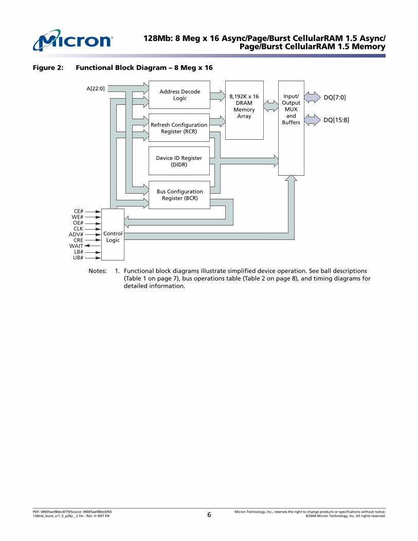
Figure 2: Functional Block Diagram – 8 Meg x 16
Notes: 1. Functional block diagrams illustrate simplified device operation. See ball descriptions (Table 1 on page 7), bus operations table (Table 2 on page 8), and timing diagrams for detailed information.
A[22:0]Input/
OutputMUXand
Buffers
ControlLogic
8,192K x 16DRAM
MemoryArray
CE#WE#OE#CLK
ADV#CRE
WAITLB#UB#
DQ[7:0]
DQ[15:8]Refresh Configuration
Register (RCR)
Device ID Register(DIDR)
Bus ConfigurationRegister (BCR)
Address DecodeLogic
PDF: 09005aef80ec6f79/Source: 09005aef80ec6f65 Micron Technology, Inc., reserves the right to change products or specifications without notice.128mb_burst_cr1_5_p26z__2.fm - Rev. H 9/07 EN 6 ©2004 Micron Technology, Inc. All rights reserved.
128Mb: 8 Meg x 16 Async/Page/Burst CellularRAM 1.5 Async/Page/Burst CellularRAM 1.5 Memory
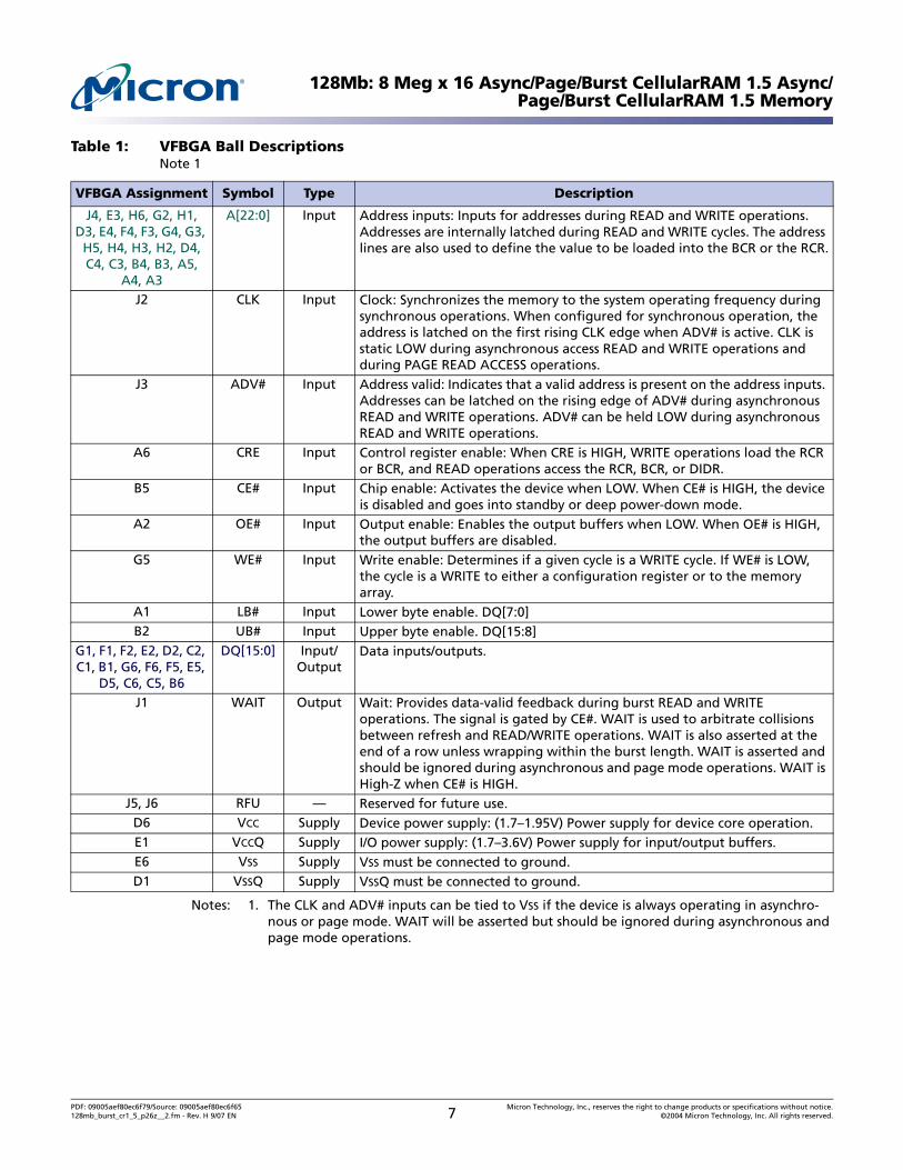
Notes: 1. The CLK and ADV# inputs can be tied to VSS if the device is always operating in asynchro-nous or page mode. WAIT will be asserted but should be ignored during asynchronous and page mode operations.
Table 1: VFBGA Ball Descriptions Note 1
VFBGA Assignment Symbol Type Description
J4, E3, H6, G2, H1, D3, E4, F4, F3, G4, G3,
H5, H4, H3, H2, D4, C4, C3, B4, B3, A5,
A4, A3
A[22:0] Input Address inputs: Inputs for addresses during READ and WRITE operations. Addresses are internally latched during READ and WRITE cycles. The address lines are also used to define the value to be loaded into the BCR or the RCR.
J2 CLK Input Clock: Synchronizes the memory to the system operating frequency during synchronous operations. When configured for synchronous operation, the address is latched on the first rising CLK edge when ADV# is active. CLK is static LOW during asynchronous access READ and WRITE operations and during PAGE READ ACCESS operations.
J3 ADV# Input Address valid: Indicates that a valid address is present on the address inputs. Addresses can be latched on the rising edge of ADV# during asynchronous READ and WRITE operations. ADV# can be held LOW during asynchronous READ and WRITE operations.
A6 CRE Input Control register enable: When CRE is HIGH, WRITE operations load the RCR or BCR, and READ operations access the RCR, BCR, or DIDR.
B5 CE# Input Chip enable: Activates the device when LOW. When CE# is HIGH, the device is disabled and goes into standby or deep power-down mode.
A2 OE# Input Output enable: Enables the output buffers when LOW. When OE# is HIGH, the output buffers are disabled.
G5 WE# Input Write enable: Determines if a given cycle is a WRITE cycle. If WE# is LOW, the cycle is a WRITE to either a configuration register or to the memory array.
A1 LB# Input Lower byte enable. DQ[7:0]B2 UB# Input Upper byte enable. DQ[15:8]
G1, F1, F2, E2, D2, C2, C1, B1, G6, F6, F5, E5,
D5, C6, C5, B6
DQ[15:0] Input/Output
Data inputs/outputs.
J1 WAIT Output Wait: Provides data-valid feedback during burst READ and WRITE operations. The signal is gated by CE#. WAIT is used to arbitrate collisions between refresh and READ/WRITE operations. WAIT is also asserted at the end of a row unless wrapping within the burst length. WAIT is asserted and should be ignored during asynchronous and page mode operations. WAIT is High-Z when CE# is HIGH.
J5, J6 RFU — Reserved for future use.D6 VCC Supply Device power supply: (1.7–1.95V) Power supply for device core operation.E1 VCCQ Supply I/O power supply: (1.7–3.6V) Power supply for input/output buffers.E6 VSS Supply VSS must be connected to ground.D1 VSSQ Supply VSSQ must be connected to ground.
PDF: 09005aef80ec6f79/Source: 09005aef80ec6f65 Micron Technology, Inc., reserves the right to change products or specifications without notice.128mb_burst_cr1_5_p26z__2.fm - Rev. H 9/07 EN 7 ©2004 Micron Technology, Inc. All rights reserved.
128Mb: 8 Meg x 16 Async/Page/Burst CellularRAM 1.5 Async/Page/Burst CellularRAM 1.5 Memory
Notes: 1. CLK must be LOW during async read and async write modes; and to achieve standby power during standby and DPD modes. CLK must be static (HIGH or LOW) during burst suspend.
2. The WAIT polarity is configured through the bus configuration register (BCR[10]).3. When LB# and UB# are in select mode (LOW), DQ[15:0] are affected. When only LB# is in
select mode, DQ[7:0] are affected. When only UB# is in the select mode, DQ[15:8] are affected.
4. The device will consume active power in this mode whenever addresses are changed.5. When the device is in standby mode, address inputs and data inputs/outputs are internally
isolated from any external influence.6. VIN = VCCQ or 0V; all device balls must be static (unswitched) in order to achieve standby cur-
rent.7. DPD is initiated when CE# transitions from LOW to HIGH after writing RCR[4] to 0. DPD is
maintained until CE# transitions from HIGH to LOW.8. Burst mode operation is initialized through the bus configuration register (BCR[15]).9. Initial cycle. Following cycles are the same as BURST CONTINUE. CE# must stay LOW for the
equivalent of a single-word burst (as indicated by WAIT).
Table 2: Bus Operations
Asynchronous ModeBCR[15] = 1 Power CLK1 ADV# CE# OE# WE# CRE
LB#/UB# WAIT2 DQ[15:0]3 Notes
Read Active L L L L H L L Low-Z Data-out 4
Write Active L L L X L L L Low-Z Data-in 4
Standby Standby L X H X X L X High-Z High-Z 5, 6
No operation Idle L X L X X L X Low-Z X 4, 6
Configuration register write
Active L L L H L H X Low-Z High-Z
Configuration register read
Active L L L L H H L Low-Z Config. reg. out
DPD Deeppower-down
L X H X X X X High-Z High-Z 7
Burst ModeBCR[15] = 0 Power CLK1 ADV# CE# OE# WE# CRE
LB#/UB# WAIT2 DQ[15:0]3 Notes
Async read Active L L L L H L L Low-Z Data-out 4
Async write Active L L L X L L L Low-Z Data-in 4
Standby Standby L X H X X L X High-Z High-Z 5, 6
No operation Idle L X L X X L X Low-Z X 4, 6
Initial burst read Active L L X H L L Low-Z X 4, 8
Initial burst write Active L L H L L X Low-Z X 4, 8
Burst continue Active H L X X X L Low-Z Data-in or Data-out
4, 8
Burst suspend Active X X L H X X X Low-Z High-Z 4, 8
Configuration register write
Active L L H L H X Low-Z High-Z 8, 9
Configuration register read
Active L L L H H L Low-Z Config. reg. out
8, 9
DPD Deeppower-down
L X H X X X X High-Z High-Z 7
PDF: 09005aef80ec6f79/Source: 09005aef80ec6f65 Micron Technology, Inc., reserves the right to change products or specifications without notice.128mb_burst_cr1_5_p26z__2.fm - Rev. H 9/07 EN 8 ©2004 Micron Technology, Inc. All rights reserved.
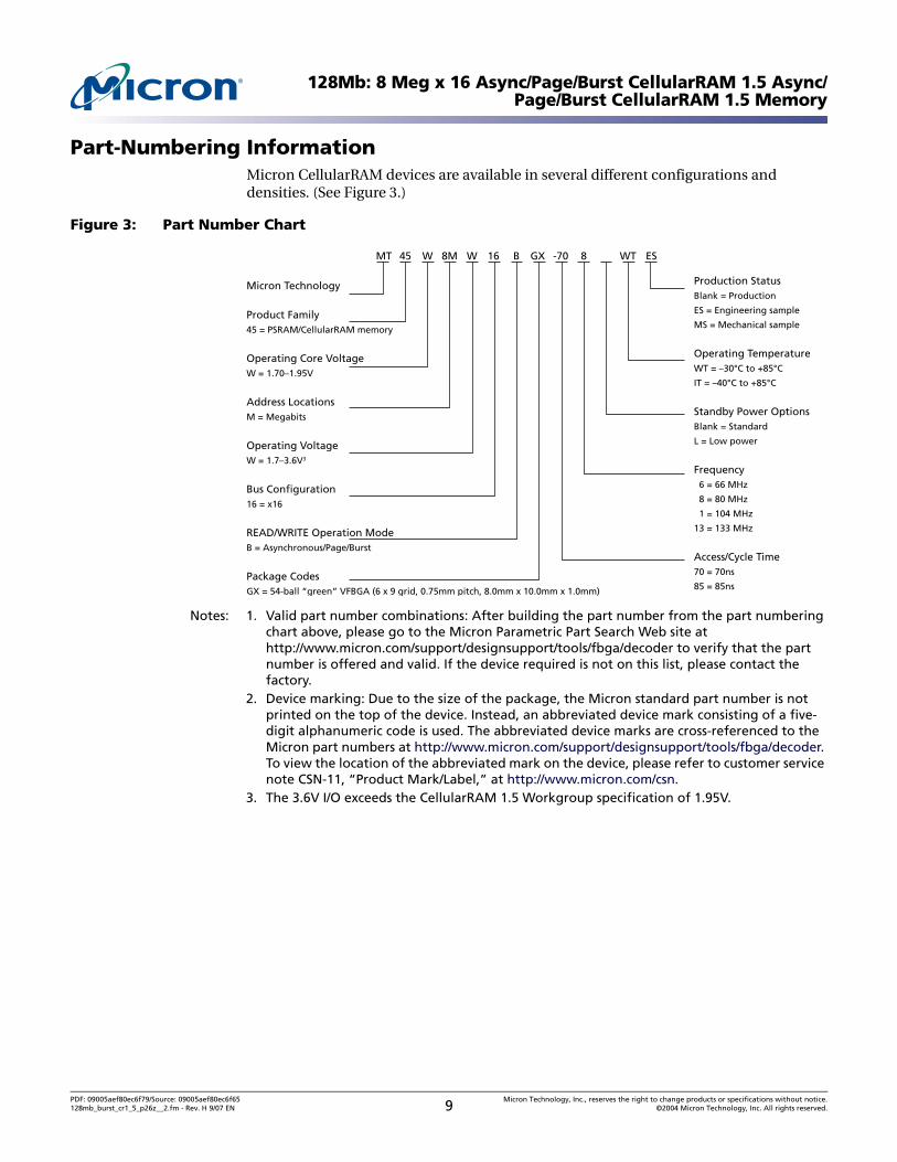
128Mb: 8 Meg x 16 Async/Page/Burst CellularRAM 1.5 Async/Page/Burst CellularRAM 1.5 Memory
Part-Numbering InformationMicron CellularRAM devices are available in several different configurations and densities. (See Figure 3.)
Figure 3: Part Number Chart
Notes: 1. Valid part number combinations: After building the part number from the part numbering chart above, please go to the Micron Parametric Part Search Web site athttp://www.micron.com/support/designsupport/tools/fbga/decoder to verify that the part number is offered and valid. If the device required is not on this list, please contact the factory.
2. Device marking: Due to the size of the package, the Micron standard part number is not printed on the top of the device. Instead, an abbreviated device mark consisting of a five-digit alphanumeric code is used. The abbreviated device marks are cross-referenced to the Micron part numbers at http://www.micron.com/support/designsupport/tools/fbga/decoder. To view the location of the abbreviated mark on the device, please refer to customer service note CSN-11, “Product Mark/Label,” at http://www.micron.com/csn.
3. The 3.6V I/O exceeds the CellularRAM 1.5 Workgroup specification of 1.95V.
MT 45 W 8M W 16 B GX -70 8 WT ES
Micron Technology
Product Family45 = PSRAM/CellularRAM memory
Operating Core VoltageW = 1.70–1.95V
Address LocationsM = Megabits
Operating VoltageW = 1.7–3.6V3
Bus Configuration16 = x16
READ/WRITE Operation ModeB = Asynchronous/Page/Burst
Package CodesGX = 54-ball “green” VFBGA (6 x 9 grid, 0.75mm pitch, 8.0mm x 10.0mm x 1.0mm)
Production StatusBlank = Production
ES = Engineering sample
MS = Mechanical sample
Operating TemperatureWT = –30°C to +85°C
IT = –40°C to +85°C
Standby Power OptionsBlank = Standard
L = Low power
Frequency 6 = 66 MHz
8 = 80 MHz
1 = 104 MHz
13 = 133 MHz
Access/Cycle Time70 = 70ns
85 = 85ns
PDF: 09005aef80ec6f79/Source: 09005aef80ec6f65 Micron Technology, Inc., reserves the right to change products or specifications without notice.128mb_burst_cr1_5_p26z__2.fm - Rev. H 9/07 EN 9 ©2004 Micron Technology, Inc. All rights reserved.
128Mb: 8 Meg x 16 Async/Page/Burst CellularRAM 1.5 Async/Page/Burst CellularRAM 1.5 Memory
Functional DescriptionIn general, the MT45W8MW16BGX device is a high-density alternative to SRAM and pseudo-SRAM products, popular in low-power, portable applications.
The MT45W8MW16BGX contains a 134,217,728-bit DRAM core, organized as 8,388,608 addresses by 16 bits. The device implements the same high-speed bus interface found on burst mode Flash products.
The CellularRAM bus interface supports both asynchronous and burst mode transfers. Page mode accesses are also included as a bandwidth-enhancing extension to the asyn-chronous read protocol.
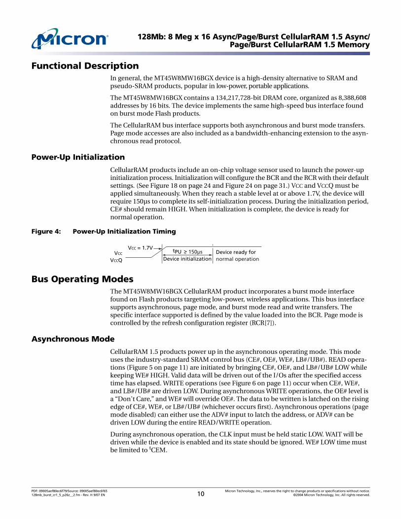
Power-Up Initialization
CellularRAM products include an on-chip voltage sensor used to launch the power-up initialization process. Initialization will configure the BCR and the RCR with their default settings. (See Figure 18 on page 24 and Figure 24 on page 31.) VCC and VCCQ must be applied simultaneously. When they reach a stable level at or above 1.7V, the device will require 150µs to complete its self-initialization process. During the initialization period, CE# should remain HIGH. When initialization is complete, the device is ready for normal operation.
Figure 4: Power-Up Initialization Timing
Bus Operating ModesThe MT45W8MW16BGX CellularRAM product incorporates a burst mode interface found on Flash products targeting low-power, wireless applications. This bus interface supports asynchronous, page mode, and burst mode read and write transfers. The specific interface supported is defined by the value loaded into the BCR. Page mode is controlled by the refresh configuration register (RCR[7]).
Asynchronous Mode
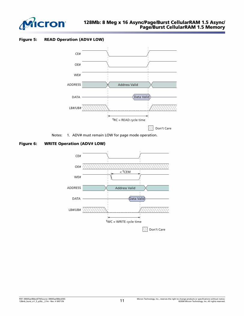
CellularRAM 1.5 products power up in the asynchronous operating mode. This mode uses the industry-standard SRAM control bus (CE#, OE#, WE#, LB#/UB#). READ opera-tions (Figure 5 on page 11) are initiated by bringing CE#, OE#, and LB#/UB# LOW while keeping WE# HIGH. Valid data will be driven out of the I/Os after the specified access time has elapsed. WRITE operations (see Figure 6 on page 11) occur when CE#, WE#, and LB#/UB# are driven LOW. During asynchronous WRITE operations, the OE# level is a “Don't Care,” and WE# will override OE#. The data to be written is latched on the rising edge of CE#, WE#, or LB#/UB# (whichever occurs first). Asynchronous operations (page mode disabled) can either use the ADV# input to latch the address, or ADV# can be driven LOW during the entire READ/WRITE operation.
During asynchronous operation, the CLK input must be held static LOW. WAIT will be driven while the device is enabled and its state should be ignored. WE# LOW time must be limited to tCEM.
VCC
VCCQ Device initialization
VCC = 1.7VDevice ready fornormal operation
tPU > 150µs
PDF: 09005aef80ec6f79/Source: 09005aef80ec6f65 Micron Technology, Inc., reserves the right to change products or specifications without notice.128mb_burst_cr1_5_p26z__2.fm - Rev. H 9/07 EN 10 ©2004 Micron Technology, Inc. All rights reserved.
128Mb: 8 Meg x 16 Async/Page/Burst CellularRAM 1.5 Async/Page/Burst CellularRAM 1.5 Memory
Figure 5: READ Operation (ADV# LOW)
Notes: 1. ADV# must remain LOW for page mode operation.
Figure 6: WRITE Operation (ADV# LOW)
Address Valid
DATA
CE#
Don’t Care
Data Valid
OE#
WE#
LB#/UB#
tRC = READ cycle time
ADDRESS
Address Valid
DATA
CE#
Don’t Care
Data Valid
OE#
WE#
LB#/UB#
tWC = WRITE cycle time
ADDRESS
< tCEM
PDF: 09005aef80ec6f79/Source: 09005aef80ec6f65 Micron Technology, Inc., reserves the right to change products or specifications without notice.128mb_burst_cr1_5_p26z__2.fm - Rev. H 9/07 EN 11 ©2004 Micron Technology, Inc. All rights reserved.
128Mb: 8 Meg x 16 Async/Page/Burst CellularRAM 1.5 Async/Page/Burst CellularRAM 1.5 Memory
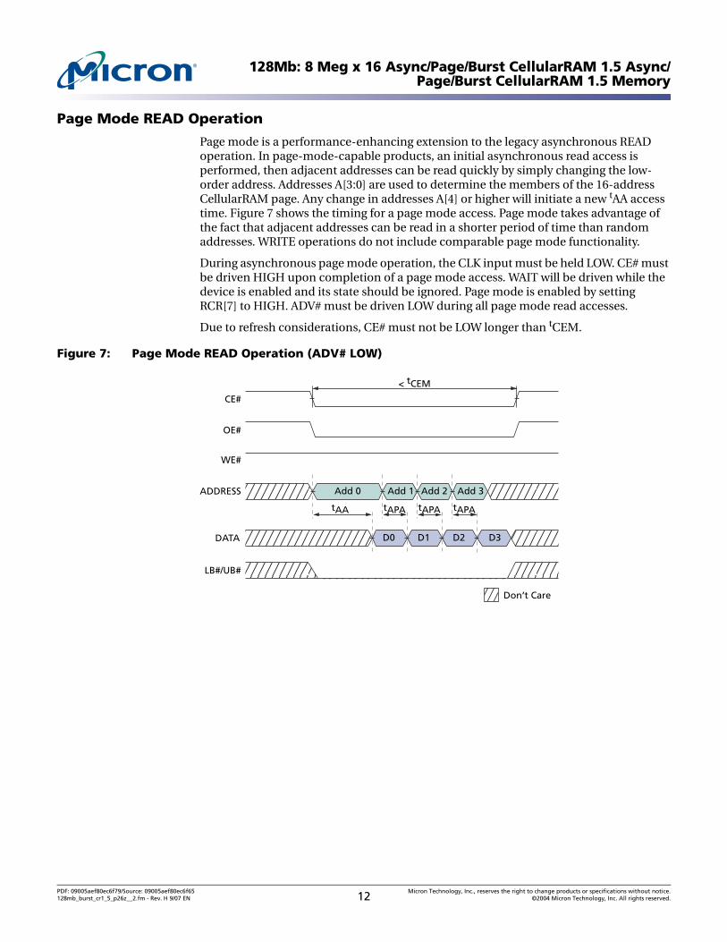
Page Mode READ Operation
Page mode is a performance-enhancing extension to the legacy asynchronous READ operation. In page-mode-capable products, an initial asynchronous read access is performed, then adjacent addresses can be read quickly by simply changing the low-order address. Addresses A[3:0] are used to determine the members of the 16-address CellularRAM page. Any change in addresses A[4] or higher will initiate a new tAA access time. Figure 7 shows the timing for a page mode access. Page mode takes advantage of the fact that adjacent addresses can be read in a shorter period of time than random addresses. WRITE operations do not include comparable page mode functionality.
During asynchronous page mode operation, the CLK input must be held LOW. CE# must be driven HIGH upon completion of a page mode access. WAIT will be driven while the device is enabled and its state should be ignored. Page mode is enabled by setting RCR[7] to HIGH. ADV# must be driven LOW during all page mode read accesses.
Due to refresh considerations, CE# must not be LOW longer than tCEM.
Figure 7: Page Mode READ Operation (ADV# LOW)
DATA
CE#
Don’t Care
OE#
WE#
LB#/UB#
ADDRESS Add 0 Add 1 Add 2 Add 3
D1 D2 D3
tAA tAPA
< tCEM
tAPA tAPA
D0
PDF: 09005aef80ec6f79/Source: 09005aef80ec6f65 Micron Technology, Inc., reserves the right to change products or specifications without notice.128mb_burst_cr1_5_p26z__2.fm - Rev. H 9/07 EN 12 ©2004 Micron Technology, Inc. All rights reserved.
128Mb: 8 Meg x 16 Async/Page/Burst CellularRAM 1.5 Async/Page/Burst CellularRAM 1.5 Memory
Burst Mode Operation
Burst mode operations enable high-speed synchronous READ and WRITE operations. Burst operations consist of a multi-clock sequence that must be performed in an ordered fashion. After CE# goes LOW, the address to access is latched on the rising edge of the next clock that ADV# is LOW. During this first clock rising edge, WE# indicates whether the operation is going to be a READ (WE# = HIGH, in Figure 8 on page 14) or WRITE (WE# = LOW, in Figure 9 on page 14).
The size of a burst can be specified in the BCR either as a fixed length or as continuous. Fixed-length bursts consist of four, eight, sixteen, or thirty-two words. Continuous bursts have the ability to start at a specified address and burst to the end of the 128-word row.
The latency count stored in the BCR defines the number of clock cycles that elapse before the initial data value is transferred between the processor and CellularRAM device. The initial latency for READ operations can be configured as fixed or variable (WRITE operations always use fixed latency). Variable latency enables the CellularRAM to be configured for minimum latency at high clock frequencies, but the controller must monitor WAIT to detect any conflict with refresh cycles.
Fixed latency outputs the first data word after the worst-case access delay, including allowance for refresh collisions. The initial latency time and clock speed determine the latency count setting. Fixed latency is used when the controller cannot monitor WAIT. Fixed latency also provides improved performance at lower clock frequencies.
The WAIT output asserts when a burst is initiated and de-asserts to indicate when data is to be transferred into (or out of) the memory. WAIT will again be asserted at the boundary of the 128-word row unless wrapping within the burst length.
To access other devices on the same bus without the timing penalty of the initial latency for a new burst, burst mode can be suspended. Bursts are suspended by stopping CLK. CLK can be stopped HIGH or LOW. If another device will use the data bus while the burst is suspended, OE# should be taken HIGH to disable the CellularRAM outputs; otherwise, OE# can remain LOW. Note that the WAIT output will continue to be active, and as a result, no other devices should directly share the WAIT connection to the controller. To continue the burst sequence, OE# is taken LOW, then CLK is restarted after valid data is available on the bus.
The CE# LOW time is limited by refresh considerations. CE# must not stay LOW longer than tCEM. If a burst suspension will cause CE# to remain LOW for longer than tCEM, CE# should be taken HIGH and the burst restarted with a new CE# LOW/ADV# LOW cycle.
PDF: 09005aef80ec6f79/Source: 09005aef80ec6f65 Micron Technology, Inc., reserves the right to change products or specifications without notice.128mb_burst_cr1_5_p26z__2.fm - Rev. H 9/07 EN 13 ©2004 Micron Technology, Inc. All rights reserved.

128Mb: 8 Meg x 16 Async/Page/Burst CellularRAM 1.5 Async/Page/Burst CellularRAM 1.5 Memory
Figure 8: Burst Mode READ (4-word burst)
Notes: 1. Non-default BCR settings for burst mode READ (4-word burst): Fixed or variable latency; latency code two (three clocks); WAIT active LOW; WAIT asserted during delay. The diagram above is representative of variable latency with no refresh collision or fixed-latency access.
Figure 9: Burst Mode WRITE (4-word burst)
Notes: 1. Non-default BCR settings for burst mode WRITE (4-word burst): Fixed or variable latency; latency code two (three clocks); WAIT active LOW; WAIT asserted during delay.
A[22:0]
D0
ADV#
CE#
OE#
D1 D2 D3
WE#
WAIT
DQ[15:0]
LB#/UB#
Latency Code 2 (3 clocks)
CLK
UndefinedDon’t CareREAD Burst Identified(WE# = HIGH)
AddressValid
A[22:0]
D0
ADV#
CE#
OE#
D1 D2 D3
WE#
WAIT
DQ[15:0]
LB#/UB#
AddressValid
Latency Code 2 (3 clocks)
CLK
Don’t CareWRITE Burst Identified(WE# = LOW)
PDF: 09005aef80ec6f79/Source: 09005aef80ec6f65 Micron Technology, Inc., reserves the right to change products or specifications without notice.128mb_burst_cr1_5_p26z__2.fm - Rev. H 9/07 EN 14 ©2004 Micron Technology, Inc. All rights reserved.
128Mb: 8 Meg x 16 Async/Page/Burst CellularRAM 1.5 Async/Page/Burst CellularRAM 1.5 Memory
Mixed-Mode Operation
The device supports a combination of synchronous READ and asynchronous READ and WRITE operations when the BCR is configured for synchronous operation. The asyn-chronous READ and WRITE operations require that the clock (CLK) remain LOW during the entire sequence. The ADV# signal can be used to latch the target address, or it can remain LOW during the entire WRITE operation. CE# can remain LOW when transi-tioning between mixed-mode operations with fixed latency enabled; however, the CE# LOW time must not exceed tCEM. Mixed-mode operation facilitates a seamless interface to legacy burst mode Flash memory controllers. See Figure 50 on page 62 for the “Asyn-chronous WRITE Followed by Burst READ” timing diagram.
WAIT Operation
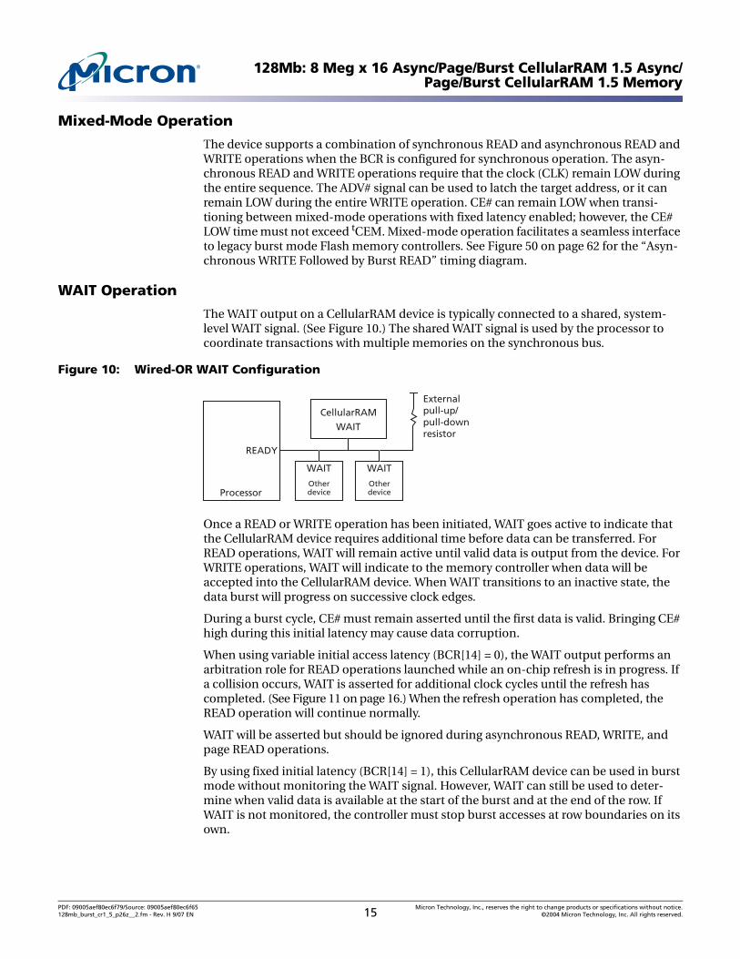
The WAIT output on a CellularRAM device is typically connected to a shared, system-level WAIT signal. (See Figure 10.) The shared WAIT signal is used by the processor to coordinate transactions with multiple memories on the synchronous bus.
Figure 10: Wired-OR WAIT Configuration
Once a READ or WRITE operation has been initiated, WAIT goes active to indicate that the CellularRAM device requires additional time before data can be transferred. For READ operations, WAIT will remain active until valid data is output from the device. For WRITE operations, WAIT will indicate to the memory controller when data will be accepted into the CellularRAM device. When WAIT transitions to an inactive state, the data burst will progress on successive clock edges.
During a burst cycle, CE# must remain asserted until the first data is valid. Bringing CE# high during this initial latency may cause data corruption.
When using variable initial access latency (BCR[14] = 0), the WAIT output performs an arbitration role for READ operations launched while an on-chip refresh is in progress. If a collision occurs, WAIT is asserted for additional clock cycles until the refresh has completed. (See Figure 11 on page 16.) When the refresh operation has completed, the READ operation will continue normally.
WAIT will be asserted but should be ignored during asynchronous READ, WRITE, and page READ operations.
By using fixed initial latency (BCR[14] = 1), this CellularRAM device can be used in burst mode without monitoring the WAIT signal. However, WAIT can still be used to deter-mine when valid data is available at the start of the burst and at the end of the row. If WAIT is not monitored, the controller must stop burst accesses at row boundaries on its own.
CellularRAM External pull-up/pull-downresistor
Processor
READY
Otherdevice
WAIT
Otherdevice
WAIT
WAIT
PDF: 09005aef80ec6f79/Source: 09005aef80ec6f65 Micron Technology, Inc., reserves the right to change products or specifications without notice.128mb_burst_cr1_5_p26z__2.fm - Rev. H 9/07 EN 15 ©2004 Micron Technology, Inc. All rights reserved.

128Mb: 8 Meg x 16 Async/Page/Burst CellularRAM 1.5 Async/Page/Burst CellularRAM 1.5 Memory
LB#/UB# Operation
The LB# enable and UB# enable signals support byte-wide data WRITEs. During WRITE operations, any disabled bytes will not be transferred to the RAM array and the internal value will remain unchanged. During an asynchronous WRITE cycle, the data to be written is latched on the rising edge of CE#, WE#, LB#, or UB#, whichever occurs first. LB# and UB# must be LOW during READ cycles.
When both the LB# and UB# are disabled (HIGH) during an operation, the device will disable the data bus from receiving or transmitting data. Although the device will seem to be deselected, it remains in an active mode as long as CE# remains LOW.
Figure 11: Refresh Collision During Variable-Latency READ Operation
Notes: 1. Non-default BCR settings for refresh collision during variable-latency READ operation: Latency code two (three clocks); WAIT active LOW; WAIT asserted during delay.
A[22:0]
ADV#
CE#
OE#
WE#
WAIT
DQ[15:0]
CLKVIH
VIL
VIH
VIL
VIH
VIL
VIH
VIL
VIH
VIL
VIH
VIL
VIH
VIL
VOH
VOL
VOH
VOL
D2D1 D3
ValidAddress
Additional WAIT states inserted to allow refresh completion.
LB#/UB#
Undefined Don’t Care
D0
High-Z
PDF: 09005aef80ec6f79/Source: 09005aef80ec6f65 Micron Technology, Inc., reserves the right to change products or specifications without notice.128mb_burst_cr1_5_p26z__2.fm - Rev. H 9/07 EN 16 ©2004 Micron Technology, Inc. All rights reserved.
128Mb: 8 Meg x 16 Async/Page/Burst CellularRAM 1.5 Async/Page/Burst CellularRAM 1.5 Memory
Low-Power Operation
Standby Mode
During standby, the device current consumption is reduced to the level necessary to perform the DRAM refresh operation. Standby operation occurs when CE# is HIGH.
The device will enter a reduced power state upon completion of a READ or WRITE oper-ation, or when the address and control inputs remain static for an extended period of time. This mode will continue until a change occurs to the address or control inputs.
Temperature-Compensated Refresh (TCR)
TCR allows for adequate refresh at different temperatures. This CellularRAM device includes an on-chip temperature sensor that automatically adjusts the refresh rate according to the operating temperature. The device continually adjusts the refresh rate to match that temperature.
Partial-Array Refresh (PAR)
PAR restricts refresh operation to a portion of the total memory array. This feature enables the device to reduce standby current by refreshing only that part of the memory array required by the host system. The refresh options are full array, one-half array, one-quarter array, one-eighth array, or none of the array. The mapping of these partitions can start at either the beginning or the end of the address map. (See Table 7 on page 32.) READ and WRITE operations to address ranges receiving refresh will not be affected. Data stored in addresses not receiving refresh will become corrupted. When re-enabling additional portions of the array, the new portions are available immediately upon writing to the RCR.
Deep Power-Down Mode (DPD)
DPD mode disables all refresh-related activity. This mode is used if the system does not require the storage provided by the CellularRAM device. Any stored data will become corrupted when DPD is enabled. When refresh activity has been re-enabled, the Cellu-larRAM device will require 150µs to perform an initialization procedure before normal operations can resume. During this 150µs period, the current consumption will be higher than the specified standby levels, but considerably lower than the active current specification.
DPD can be enabled by writing to the RCR using CRE or the software access sequence; DPD starts when CE# goes HIGH. DPD is disabled the next time CE# goes LOW and stays LOW for at least 10µs.
RegistersTwo user-accessible configuration registers define the device operation. The BCR defines how the CellularRAM interacts with the system memory bus and is nearly identical to its counterpart on burst mode Flash devices. The RCR is used to control how refresh is performed on the DRAM array. These registers are automatically loaded with default settings during power-up, and can be updated any time the devices are operating in a standby state.
A DIDR provides information on the device manufacturer, CellularRAM generation, and the specific device configuration. The DIDR is read-only.
PDF: 09005aef80ec6f79/Source: 09005aef80ec6f65 Micron Technology, Inc., reserves the right to change products or specifications without notice.128mb_burst_cr1_5_p26z__2.fm - Rev. H 9/07 EN 17 ©2004 Micron Technology, Inc. All rights reserved.

128Mb: 8 Meg x 16 Async/Page/Burst CellularRAM 1.5 Async/Page/Burst CellularRAM 1.5 Memory
Access Using CRE
The registers can be accessed using either a synchronous or an asynchronous operation when the control register enable (CRE) input is HIGH. (See Figures 12 through 15 on pages 18 through 21.) When CRE is LOW, a READ or WRITE operation will access the memory array. The configuration register values are written via addresses A[22:0]. In an asynchronous WRITE, the values are latched into the configuration register on the rising edge of ADV#, CE#, or WE#, whichever occurs first; LB# and UB# are “Don’t Care.” The BCR is accessed when A[19:18] are 10b; the RCR is accessed when A[19:18] are 00b. The DIDR is read when A[19:18] are 01b. For reads, address inputs other than A[19:18] are “Don’t Care,” and register bits 15:0 are output on DQ[15:0]. Micron strongly recommends reading the memory array immediately after performing a configuration register READ or WRITE operation.
Figure 12: Configuration Register WRITE, Asynchronous Mode, Followed by READ ARRAY Operation
Notes: 1. A[19:18] = 00b to load RCR, and 10b to load BCR.
A[22:0](except A[19:18]) OPCODE Address
Address
Data Valid
A[19:18]1
ADV#
CE#
OE#
WE#
LB#/UB#
DQ[15:0]
Initiate Control Register Access
Write Address Bus Valueto Control Register
CRE
tAVStAVH
tAVH
tAVS
tVP tCPH
tWP
tCW
Don’t Care
Select Control Register
PDF: 09005aef80ec6f79/Source: 09005aef80ec6f65 Micron Technology, Inc., reserves the right to change products or specifications without notice.128mb_burst_cr1_5_p26z__2.fm - Rev. H 9/07 EN 18 ©2004 Micron Technology, Inc. All rights reserved.
128Mb: 8 Meg x 16 Async/Page/Burst CellularRAM 1.5 Async/Page/Burst CellularRAM 1.5 Memory
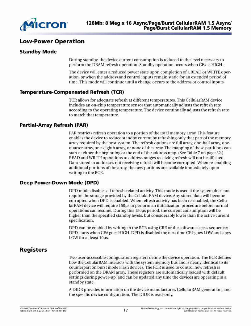
Figure 13: Configuration Register WRITE, Synchronous Mode Followed by READ ARRAY Operation
Notes: 1. Non-default BCR settings for synchronous mode configuration register WRITE followed by READ ARRAY operation: Latency code two (three clocks); WAIT active LOW; WAIT asserted during delay.
2. A[19:18] = 00b to load RCR, and 10b to load BCR.3. CE# must remain LOW to complete a burst-of-one WRITE. WAIT must be monitored—addi-
tional WAIT cycles caused by refresh collisions require a corresponding number of addi-tional CE# LOW cycles.
CLK
A[22:0](except A[19:18])
A[19:18]2
CRE
ADV#
CE#
OE#
WE#
LB#/UB#
WAIT
DQ[15:0]
tSP
tSP
tSP
tHD
tHD
tHD
tCSP
tSP
tHD
High-Z
Don’t Care
OPCODE Address
High-ZtCEW
Latch Control Register Address
tCBPH3
DataValid
Address
Latch Control Register Value
PDF: 09005aef80ec6f79/Source: 09005aef80ec6f65 Micron Technology, Inc., reserves the right to change products or specifications without notice.128mb_burst_cr1_5_p26z__2.fm - Rev. H 9/07 EN 19 ©2004 Micron Technology, Inc. All rights reserved.
128Mb: 8 Meg x 16 Async/Page/Burst CellularRAM 1.5 Async/Page/Burst CellularRAM 1.5 Memory
Figure 14: Register READ, Asynchronous Mode Followed by READ ARRAY Operation
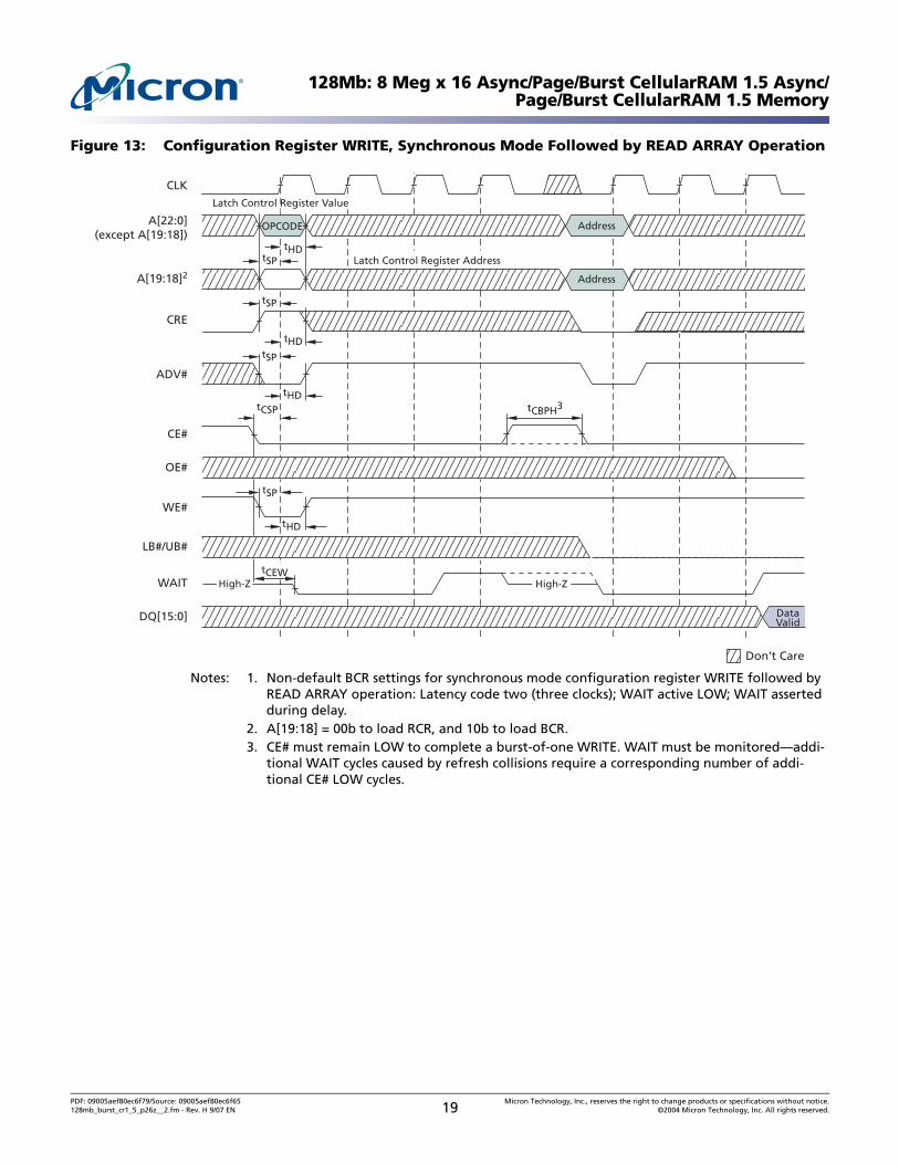
Notes: 1. A[19:18] = 00b to read RCR, 10b to read BCR, and 01b to read DIDR.
A[22:0](except A[19:18]) Address
Address
Data ValidCR Valid
A[19:18]1
ADV#
CE#
OE#
WE#
LB#/UB#
DQ[15:0]
Initiate Register Access
CRE
tAVH
tAVS
tAA
tVP
tCPH
tCO
tOLZ
tBA
tLZ
tOE
tLZ
UndefinedDon’t Care
Select Register
tAAVD
tAVS
tAA
tHZ
tOHZ
tBHZ
tAVH
PDF: 09005aef80ec6f79/Source: 09005aef80ec6f65 Micron Technology, Inc., reserves the right to change products or specifications without notice.128mb_burst_cr1_5_p26z__2.fm - Rev. H 9/07 EN 20 ©2004 Micron Technology, Inc. All rights reserved.
128Mb: 8 Meg x 16 Async/Page/Burst CellularRAM 1.5 Async/Page/Burst CellularRAM 1.5 Memory
Figure 15: Register READ, Synchronous Mode Followed by READ ARRAY Operation
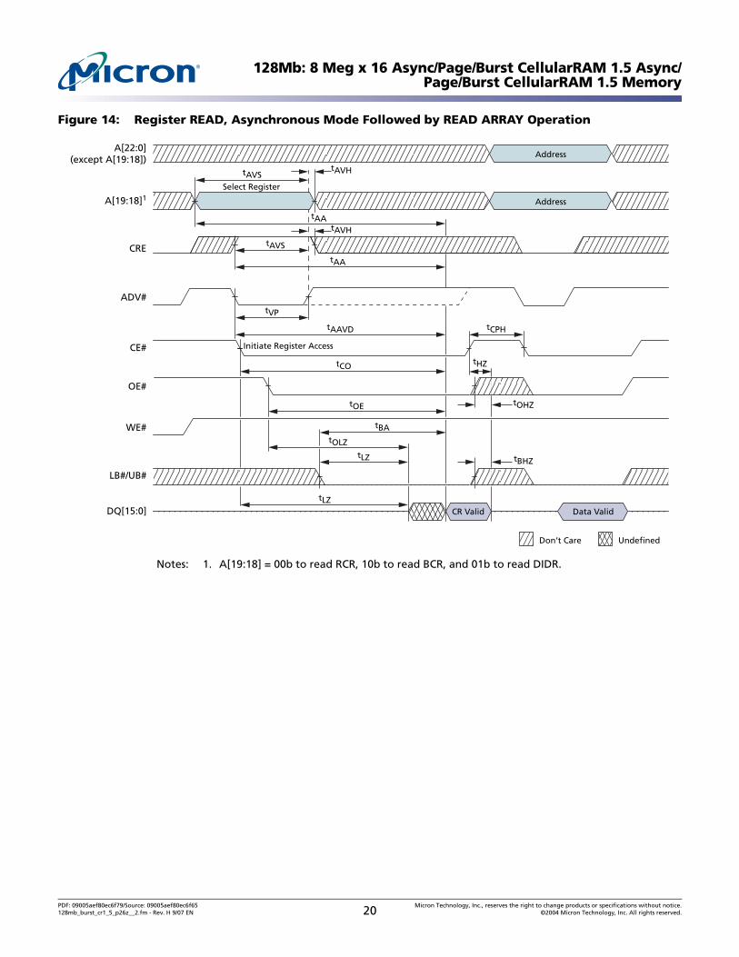
Notes: 1. Non-default BCR settings for synchronous mode register READ followed by READ ARRAY operation: Latency code two (three clocks); WAIT active LOW; WAIT asserted during delay.
2. A[19:18] = 00b to read RCR, 10b to read BCR, and 01b to read DIDR.3. CE# must remain LOW to complete a burst-of-one READ. WAIT must be monitored—addi-
tional WAIT cycles caused by refresh collisions require a corresponding number of addi-tional CE# LOW cycles.
CLK
A[22:0] (except A[19:18])
A[19:18]2
CRE
ADV#
CE#
OE#
WE#
LB#/UB#
WAIT
DQ[15:0]
tSP
tSP
tSP
tHD
tHD
tHD
tHZ
tCSP
tKOH
UndefinedDon’t Care
tSP tHD
Address
tCEW
Latch Control Register Value
tOLZ
Latch Control Register Address
tCBPH3
tBOE
Data Valid
Address
tACLK
tOHZ
High-Z High-Z
tABA
CR Valid
PDF: 09005aef80ec6f79/Source: 09005aef80ec6f65 Micron Technology, Inc., reserves the right to change products or specifications without notice.128mb_burst_cr1_5_p26z__2.fm - Rev. H 9/07 EN 21 ©2004 Micron Technology, Inc. All rights reserved.
128Mb: 8 Meg x 16 Async/Page/Burst CellularRAM 1.5 Async/Page/Burst CellularRAM 1.5 Memory
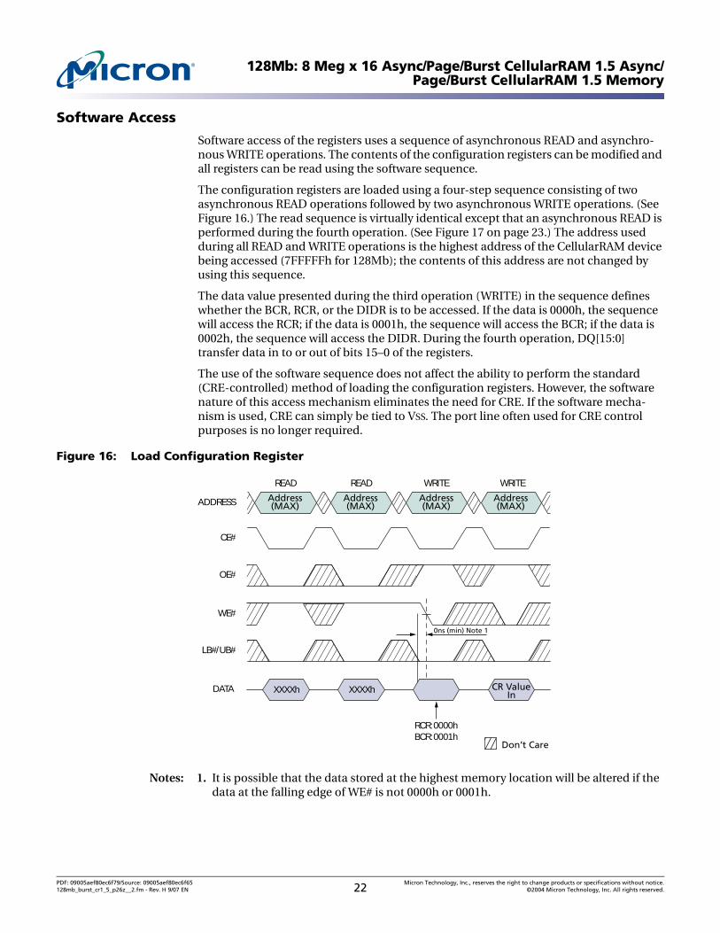
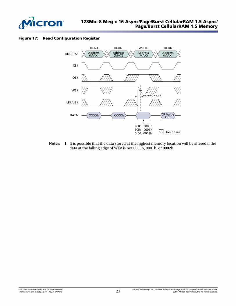
Software Access
Software access of the registers uses a sequence of asynchronous READ and asynchro-nous WRITE operations. The contents of the configuration registers can be modified and all registers can be read using the software sequence.
The configuration registers are loaded using a four-step sequence consisting of two asynchronous READ operations followed by two asynchronous WRITE operations. (See Figure 16.) The read sequence is virtually identical except that an asynchronous READ is performed during the fourth operation. (See Figure 17 on page 23.) The address used during all READ and WRITE operations is the highest address of the CellularRAM device being accessed (7FFFFFh for 128Mb); the contents of this address are not changed by using this sequence.
The data value presented during the third operation (WRITE) in the sequence defines whether the BCR, RCR, or the DIDR is to be accessed. If the data is 0000h, the sequence will access the RCR; if the data is 0001h, the sequence will access the BCR; if the data is 0002h, the sequence will access the DIDR. During the fourth operation, DQ[15:0] transfer data in to or out of bits 15–0 of the registers.
The use of the software sequence does not affect the ability to perform the standard (CRE-controlled) method of loading the configuration registers. However, the software nature of this access mechanism eliminates the need for CRE. If the software mecha-nism is used, CRE can simply be tied to VSS. The port line often used for CRE control purposes is no longer required.
Figure 16: Load Configuration Register
Notes: 1. It is possible that the data stored at the highest memory location will be altered if the data at the falling edge of WE# is not 0000h or 0001h.
Address (MAX)
Address (MAX)
Address (MAX)
Address (MAX)
XXXXh XXXXh
RCR: 0000h BCR: 0001h
CR Value In
ADDRESS
CE#
OE#
WE#
LB#/UB#
DATA
Don’t Care
READ READ WRITE WRITE
0ns (min) Note 1
PDF: 09005aef80ec6f79/Source: 09005aef80ec6f65 Micron Technology, Inc., reserves the right to change products or specifications without notice.128mb_burst_cr1_5_p26z__2.fm - Rev. H 9/07 EN 22 ©2004 Micron Technology, Inc. All rights reserved.
128Mb: 8 Meg x 16 Async/Page/Burst CellularRAM 1.5 Async/Page/Burst CellularRAM 1.5 Memory
Figure 17: Read Configuration Register
Notes: 1. It is possible that the data stored at the highest memory location will be altered if the data at the falling edge of WE# is not 0000h, 0001h, or 0002h.
Address (MAX)
Address (MAX)
Address (MAX)
Address (MAX)
XXXXh XXXXh CR Value Out
ADDRESS
CE#
OE#
WE#
LB#/UB#
DATA
Don't Care
READ READ WRITE READ
RCR: 0000h BCR: 0001h DIDR: 0002h
0ns (min) Note 1
PDF: 09005aef80ec6f79/Source: 09005aef80ec6f65 Micron Technology, Inc., reserves the right to change products or specifications without notice.128mb_burst_cr1_5_p26z__2.fm - Rev. H 9/07 EN 23 ©2004 Micron Technology, Inc. All rights reserved.

128Mb: 8 Meg x 16 Async/Page/Burst CellularRAM 1.5 Async/Page/Burst CellularRAM 1.5 Memory
Bus Configuration Register (BCR)
The BCR defines how the CellularRAM device interacts with the system memory bus. Page mode operation is enabled by a bit contained in the RCR. Figure 18 describes the control bits in the BCR. At power-up, the BCR is set to 9D1Fh.
The BCR is accessed with CRE HIGH and A[19:18] = 10b or through the register access software sequence with DQ = 0001h on the third cycle.
Figure 18: Bus Configuration Register Definition
Notes: 1. Burst wrap and length apply to both READ and WRITE operations.
A13
13 12 11 0 Latency Counter
Initial Latency
3 2 1 WAIT
Polarity
4 5 WAIT
Configuration (WC)
6 7 8
Drive Strength Burst
Wrap (BW)
14
A12 A11 A10 A9 A8 A7 A6 A5 A4 A3 A2 A1 A0
0 1
Operating Mode
Synchronous burst access mode Asynchronous access mode (default)
BCR[12] BCR[11] Latency Counter BCR[13]
0
0
0
0
1
1
1
1
0
0
1
1
0
0
1
1
0
1
0
1
0
1
0
1
Code 8
Code 1–Reserved
Code 2
Code 3 (Default)
Code 4
Code 5
Code 6
Code 7–Reserved
0
1
WAIT Polarity
Active LOW
Active HIGH (default)
BCR[10]
0 1
WAIT Configuration
Asserted during delay
Asserted one data cycle before delay (default)
Drive Strength
Full
1/2 (default)
1/4
Reserved
BCR[5]
0
0
1
1
BCR[4]
0
1
0
1
0
1
Initial Access Latency
Variable (default)
Fixed
BCR[14]
Burst Wrap (Note 1)
Burst wraps within the burst length
Burst no wrap (default)
BCR[3]
BCR[1] BCR[0] Burst Length (Note 1) BCR[2]
15 Burst
Length (BL)Reserved Reserved
9 10 Operating
Mode Reserved
22–20
A14 A15 A[17:16]
0 1
0
Register Select
Select RCR
Select BCR
Select DIDR
19–18 17–16 Register Select Reserved
A[19:18] A[22:20]
Reserved
Must be set to “0”Must be set to “0”Must be set to “0”All must be set to “0”
BCR[8]
BCR[15]
BCR[19]
0 0
1
BCR[18]
0
1
0
0
0
1
1
0
1
1
0
1
Others
1
0
1
0
1
4 words
8 words
16 words
32 words
Continuous burst (default)
Reserved
Setting is ignored(Default to “0”)
11
PDF: 09005aef80ec6f79/Source: 09005aef80ec6f65 Micron Technology, Inc., reserves the right to change products or specifications without notice.128mb_burst_cr1_5_p26z__2.fm - Rev. H 9/07 EN 24 ©2004 Micron Technology, Inc. All rights reserved.
128Mb: 8 Meg x 16 Async/Page/Burst CellularRAM 1.5 Async/Page/Burst CellularRAM 1.5 Memory
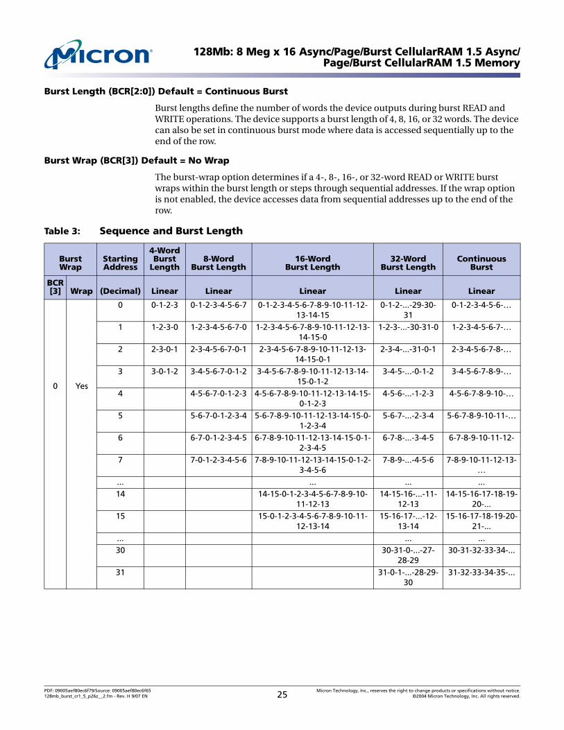
Burst Length (BCR[2:0]) Default = Continuous Burst
Burst lengths define the number of words the device outputs during burst READ and WRITE operations. The device supports a burst length of 4, 8, 16, or 32 words. The device can also be set in continuous burst mode where data is accessed sequentially up to the end of the row.
Burst Wrap (BCR[3]) Default = No Wrap
The burst-wrap option determines if a 4-, 8-, 16-, or 32-word READ or WRITE burst wraps within the burst length or steps through sequential addresses. If the wrap option is not enabled, the device accesses data from sequential addresses up to the end of the row.
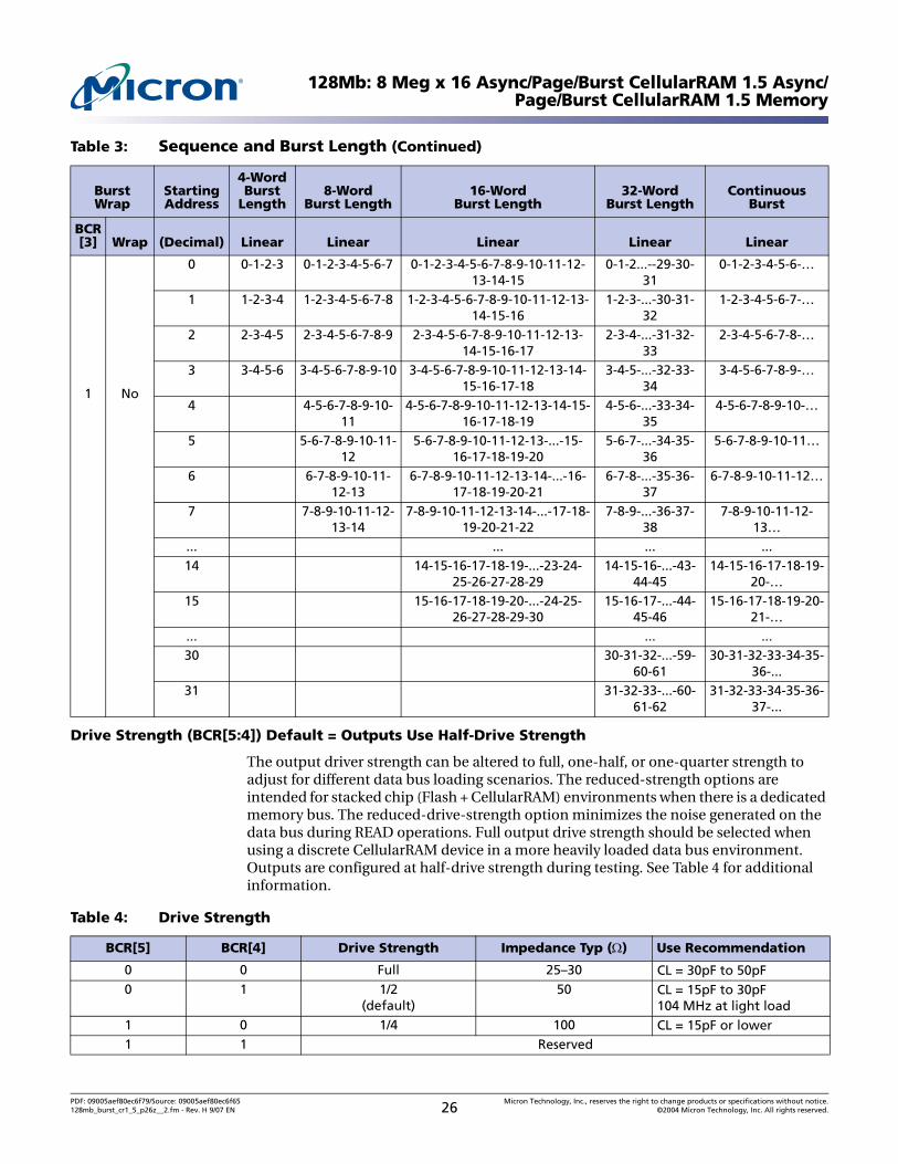
Table 3: Sequence and Burst Length
Burst Wrap
StartingAddress
4-Word Burst
Length8-Word
Burst Length16-Word
Burst Length32-Word
Burst LengthContinuous
Burst
BCR[3] Wrap (Decimal) Linear Linear Linear Linear Linear
0 Yes
0 0-1-2-3 0-1-2-3-4-5-6-7 0-1-2-3-4-5-6-7-8-9-10-11-12-13-14-15
0-1-2-...-29-30-31
0-1-2-3-4-5-6-…
1 1-2-3-0 1-2-3-4-5-6-7-0 1-2-3-4-5-6-7-8-9-10-11-12-13-14-15-0
1-2-3-...-30-31-0 1-2-3-4-5-6-7-…
2 2-3-0-1 2-3-4-5-6-7-0-1 2-3-4-5-6-7-8-9-10-11-12-13-14-15-0-1
2-3-4-...-31-0-1 2-3-4-5-6-7-8-…
3 3-0-1-2 3-4-5-6-7-0-1-2 3-4-5-6-7-8-9-10-11-12-13-14-15-0-1-2
3-4-5-...-0-1-2 3-4-5-6-7-8-9-…
4 4-5-6-7-0-1-2-3 4-5-6-7-8-9-10-11-12-13-14-15-0-1-2-3
4-5-6-...-1-2-3 4-5-6-7-8-9-10-…
5 5-6-7-0-1-2-3-4 5-6-7-8-9-10-11-12-13-14-15-0-1-2-3-4
5-6-7-...-2-3-4 5-6-7-8-9-10-11-…
6 6-7-0-1-2-3-4-5 6-7-8-9-10-11-12-13-14-15-0-1-2-3-4-5
6-7-8-...-3-4-5 6-7-8-9-10-11-12-
7 7-0-1-2-3-4-5-6 7-8-9-10-11-12-13-14-15-0-1-2-3-4-5-6
7-8-9-...-4-5-6 7-8-9-10-11-12-13-…
... ... ... ...14 14-15-0-1-2-3-4-5-6-7-8-9-10-
11-12-1314-15-16-...-11-
12-1314-15-16-17-18-19-
20-...15 15-0-1-2-3-4-5-6-7-8-9-10-11-
12-13-1415-16-17-...-12-
13-1415-16-17-18-19-20-
21-...... ... ...30 30-31-0-...-27-
28-2930-31-32-33-34-...
31 31-0-1-...-28-29-30
31-32-33-34-35-...
PDF: 09005aef80ec6f79/Source: 09005aef80ec6f65 Micron Technology, Inc., reserves the right to change products or specifications without notice.128mb_burst_cr1_5_p26z__2.fm - Rev. H 9/07 EN 25 ©2004 Micron Technology, Inc. All rights reserved.
128Mb: 8 Meg x 16 Async/Page/Burst CellularRAM 1.5 Async/Page/Burst CellularRAM 1.5 Memory
Drive Strength (BCR[5:4]) Default = Outputs Use Half-Drive Strength
The output driver strength can be altered to full, one-half, or one-quarter strength to adjust for different data bus loading scenarios. The reduced-strength options are intended for stacked chip (Flash + CellularRAM) environments when there is a dedicated memory bus. The reduced-drive-strength option minimizes the noise generated on the data bus during READ operations. Full output drive strength should be selected when using a discrete CellularRAM device in a more heavily loaded data bus environment. Outputs are configured at half-drive strength during testing. See Table 4 for additional information.
1 No
0 0-1-2-3 0-1-2-3-4-5-6-7 0-1-2-3-4-5-6-7-8-9-10-11-12-13-14-15
0-1-2...--29-30-31
0-1-2-3-4-5-6-…
1 1-2-3-4 1-2-3-4-5-6-7-8 1-2-3-4-5-6-7-8-9-10-11-12-13-14-15-16
1-2-3-...-30-31-32
1-2-3-4-5-6-7-…
2 2-3-4-5 2-3-4-5-6-7-8-9 2-3-4-5-6-7-8-9-10-11-12-13-14-15-16-17
2-3-4-...-31-32-33
2-3-4-5-6-7-8-…
3 3-4-5-6 3-4-5-6-7-8-9-10 3-4-5-6-7-8-9-10-11-12-13-14-15-16-17-18
3-4-5-...-32-33-34
3-4-5-6-7-8-9-…
4 4-5-6-7-8-9-10-11
4-5-6-7-8-9-10-11-12-13-14-15-16-17-18-19
4-5-6-...-33-34-35
4-5-6-7-8-9-10-…
5 5-6-7-8-9-10-11-12
5-6-7-8-9-10-11-12-13-...-15-16-17-18-19-20
5-6-7-...-34-35-36
5-6-7-8-9-10-11…
6 6-7-8-9-10-11-12-13
6-7-8-9-10-11-12-13-14-...-16-17-18-19-20-21
6-7-8-...-35-36-37
6-7-8-9-10-11-12…
7 7-8-9-10-11-12-13-14
7-8-9-10-11-12-13-14-...-17-18-19-20-21-22
7-8-9-...-36-37-38
7-8-9-10-11-12-13…
... ... ... ...14 14-15-16-17-18-19-...-23-24-
25-26-27-28-2914-15-16-...-43-
44-4514-15-16-17-18-19-
20-…15 15-16-17-18-19-20-...-24-25-
26-27-28-29-3015-16-17-...-44-
45-4615-16-17-18-19-20-
21-…... ... ...30 30-31-32-...-59-
60-6130-31-32-33-34-35-
36-...31 31-32-33-...-60-
61-6231-32-33-34-35-36-
37-...
Table 4: Drive Strength
BCR[5] BCR[4] Drive Strength Impedance Typ (Ω) Use Recommendation
0 0 Full 25–30 CL = 30pF to 50pF0 1 1/2
(default)50 CL = 15pF to 30pF
104 MHz at light load1 0 1/4 100 CL = 15pF or lower1 1 Reserved
Table 3: Sequence and Burst Length (Continued)
Burst Wrap
StartingAddress
4-Word Burst
Length8-Word
Burst Length16-Word
Burst Length32-Word
Burst LengthContinuous
Burst
BCR[3] Wrap (Decimal) Linear Linear Linear Linear Linear
PDF: 09005aef80ec6f79/Source: 09005aef80ec6f65 Micron Technology, Inc., reserves the right to change products or specifications without notice.128mb_burst_cr1_5_p26z__2.fm - Rev. H 9/07 EN 26 ©2004 Micron Technology, Inc. All rights reserved.
128Mb: 8 Meg x 16 Async/Page/Burst CellularRAM 1.5 Async/Page/Burst CellularRAM 1.5 Memory
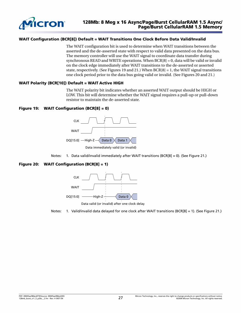
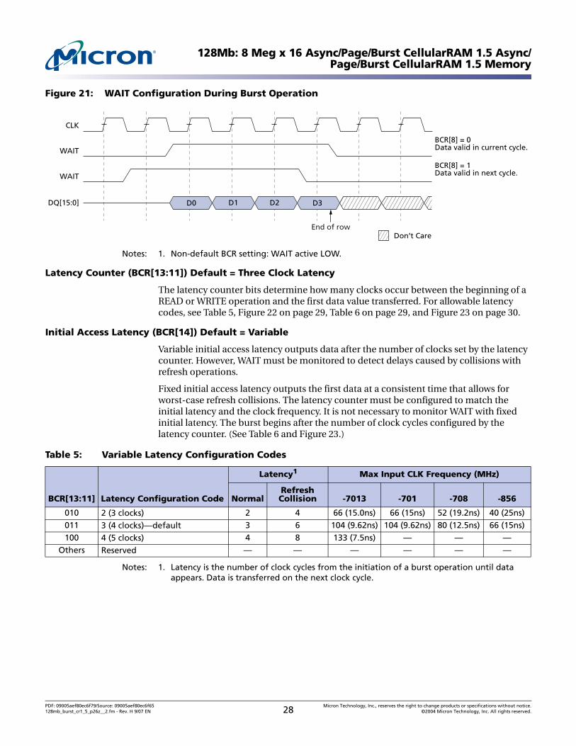
WAIT Configuration (BCR[8]) Default = WAIT Transitions One Clock Before Data Valid/Invalid
The WAIT configuration bit is used to determine when WAIT transitions between the asserted and the de-asserted state with respect to valid data presented on the data bus. The memory controller will use the WAIT signal to coordinate data transfer during synchronous READ and WRITE operations. When BCR[8] = 0, data will be valid or invalid on the clock edge immediately after WAIT transitions to the de-asserted or asserted state, respectively. (See Figures 19 and 21.) When BCR[8] = 1, the WAIT signal transitions one clock period prior to the data bus going valid or invalid. (See Figures 20 and 21.)
WAIT Polarity (BCR[10]) Default = WAIT Active HIGH
The WAIT polarity bit indicates whether an asserted WAIT output should be HIGH or LOW. This bit will determine whether the WAIT signal requires a pull-up or pull-down resistor to maintain the de-asserted state.
Figure 19: WAIT Configuration (BCR[8] = 0)
Notes: 1. Data valid/invalid immediately after WAIT transitions (BCR[8] = 0). (See Figure 21.)
Figure 20: WAIT Configuration (BCR[8] = 1)
Notes: 1. Valid/invalid data delayed for one clock after WAIT transitions (BCR[8] = 1). (See Figure 21.)
WAIT
DQ[15:0]
CLK
Data 0 Data 1
Data immediately valid (or invalid)
High-Z
WAIT
DQ[15:0]
CLK
Data 0
Data valid (or invalid) after one clock delay
High-Z
PDF: 09005aef80ec6f79/Source: 09005aef80ec6f65 Micron Technology, Inc., reserves the right to change products or specifications without notice.128mb_burst_cr1_5_p26z__2.fm - Rev. H 9/07 EN 27 ©2004 Micron Technology, Inc. All rights reserved.
128Mb: 8 Meg x 16 Async/Page/Burst CellularRAM 1.5 Async/Page/Burst CellularRAM 1.5 Memory
Figure 21: WAIT Configuration During Burst Operation
Notes: 1. Non-default BCR setting: WAIT active LOW.
Latency Counter (BCR[13:11]) Default = Three Clock Latency
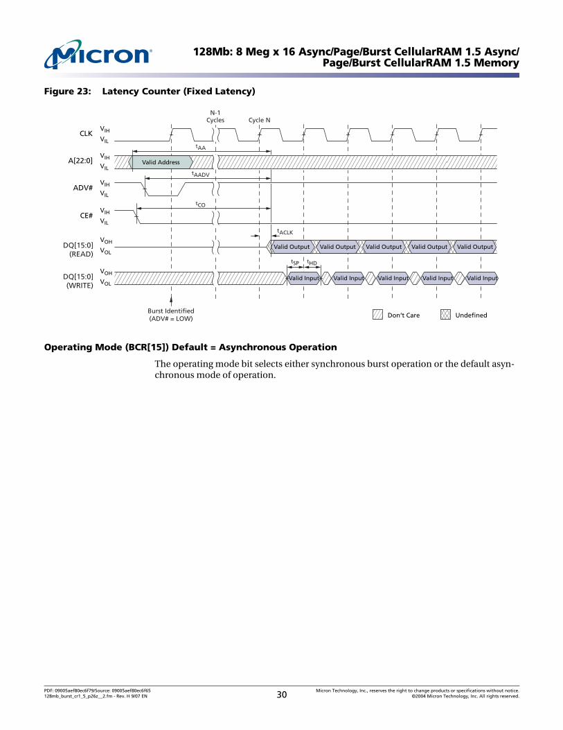
The latency counter bits determine how many clocks occur between the beginning of a READ or WRITE operation and the first data value transferred. For allowable latency codes, see Table 5, Figure 22 on page 29, Table 6 on page 29, and Figure 23 on page 30.
Initial Access Latency (BCR[14]) Default = Variable
Variable initial access latency outputs data after the number of clocks set by the latency counter. However, WAIT must be monitored to detect delays caused by collisions with refresh operations.
Fixed initial access latency outputs the first data at a consistent time that allows for worst-case refresh collisions. The latency counter must be configured to match the initial latency and the clock frequency. It is not necessary to monitor WAIT with fixed initial latency. The burst begins after the number of clock cycles configured by the latency counter. (See Table 6 and Figure 23.)
Notes: 1. Latency is the number of clock cycles from the initiation of a burst operation until data appears. Data is transferred on the next clock cycle.
Table 5: Variable Latency Configuration Codes
BCR[13:11] Latency Configuration Code
Latency1 Max Input CLK Frequency (MHz)
NormalRefresh Collision -7013 -701 -708 -856
010 2 (3 clocks) 2 4 66 (15.0ns) 66 (15ns) 52 (19.2ns) 40 (25ns)011 3 (4 clocks)—default 3 6 104 (9.62ns) 104 (9.62ns) 80 (12.5ns) 66 (15ns)100 4 (5 clocks) 4 8 133 (7.5ns) — — —
Others Reserved — — — — — —
WAIT
WAIT
DQ[15:0]
CLK
D0
BCR[8] = 0Data valid in current cycle.
BCR[8] = 1Data valid in next cycle.
Don’t Care
D1 D2 D3
End of row
PDF: 09005aef80ec6f79/Source: 09005aef80ec6f65 Micron Technology, Inc., reserves the right to change products or specifications without notice.128mb_burst_cr1_5_p26z__2.fm - Rev. H 9/07 EN 28 ©2004 Micron Technology, Inc. All rights reserved.

128Mb: 8 Meg x 16 Async/Page/Burst CellularRAM 1.5 Async/Page/Burst CellularRAM 1.5 Memory
Figure 22: Latency Counter (Variable Initial Latency, No Refresh Collision)
Table 6: Fixed Latency Configuration Codes
BCR[13:11] Latency Configuration Code Latency Count (N)
Max Input CLK Frequency (MHz)
-7013 -701 -708 -856
010 2 (3 clocks) 2 33 (30ns) 33 (30ns) 33 (30ns) 20 (50ns)011 3 (4 clocks)—default 3 52 (19.2ns) 52 (19.2ns) 52 (19.2ns) 33 (30ns)100 4 (5 clocks) 4 66 (15ns) 66 (15ns) 66 (15ns) 40 (25ns)101 5 (6 clocks) 5 75 (13.3ns) 75 (13.3ns) 75 (13.3ns) 52 (19.2ns)110 6 (7 clocks) 6 104 (9.62ns)
104 (9.62ns) 80 (12.5ns) 66 (15ns)000 8 (9 clocks) 8 133 (7.5ns)Others Reserved — — — — —
A[22:0]
ADV#
DQ[15:0]
CLK
Code 2
Valid Output Valid Output Valid OutputValid OutputValid Output
Valid Output Valid OutputValid OutputValid Output
Code 3 (Default)
DQ[15:0]
Don’t Care Undefined
VIH
VIL
VIH
VIL
VIH
VIL
VOH
VOL
VOH
VOL
Valid Address
PDF: 09005aef80ec6f79/Source: 09005aef80ec6f65 Micron Technology, Inc., reserves the right to change products or specifications without notice.128mb_burst_cr1_5_p26z__2.fm - Rev. H 9/07 EN 29 ©2004 Micron Technology, Inc. All rights reserved.
128Mb: 8 Meg x 16 Async/Page/Burst CellularRAM 1.5 Async/Page/Burst CellularRAM 1.5 Memory
Figure 23: Latency Counter (Fixed Latency)
Operating Mode (BCR[15]) Default = Asynchronous Operation
The operating mode bit selects either synchronous burst operation or the default asyn-chronous mode of operation.
A[22:0]
ADV#
DQ[15:0](READ)
CLK
Valid Output Valid Output Valid OutputValid OutputValid Output
Don’t Care Undefined
VIH
VIL
VIH
VIL
VIH
VIL
CE#VIH
VIL
VOH
VOL
tAADV
tAA
tCO
tACLK
tSP tHD
DQ[15:0](WRITE)
VOH
VOL
N-1Cycles Cycle N
Valid Input Valid Input Valid Input Valid Input Valid Input
Burst Identified(ADV# = LOW)
Valid Address
PDF: 09005aef80ec6f79/Source: 09005aef80ec6f65 Micron Technology, Inc., reserves the right to change products or specifications without notice.128mb_burst_cr1_5_p26z__2.fm - Rev. H 9/07 EN 30 ©2004 Micron Technology, Inc. All rights reserved.

128Mb: 8 Meg x 16 Async/Page/Burst CellularRAM 1.5 Async/Page/Burst CellularRAM 1.5 Memory
Refresh Configuration Register (RCR)
The RCR defines how the CellularRAM device performs its transparent self refresh. Altering the refresh parameters can dramatically reduce current consumption during standby mode. Page mode control is also embedded into the RCR. Figure 24 describes the control bits used in the RCR. At power-up, the RCR is set to 0010h.
The RCR is accessed with CRE HIGH and A[19:18] = 00b or through the register access software sequence with DQ = 0000h on the third cycle. (See “Registers” on page 17.)
PAR (RCR[2:0]) Default = Full Array Refresh
The PAR bits restrict refresh operation to a portion of the total memory array. This feature allows the device to reduce standby current by refreshing only that part of the memory array required by the host system. The refresh options are full array, one-half array, one-quarter array, one-eighth array, or none of the array. The mapping of these partitions can start at either the beginning or the end of the address map. (See Table 12 on page 36.)
Figure 24: Refresh Configuration Register Mapping
PAR
A4 A3 A2 A1 A0 Address Bus
45 123 06
A5
0
1
Deep Power-Down
DPD enable
DPD disable (default)
RCR[4]
A6
All must be set to “0”
A[17:8]
17–819–1822–20
RegisterSelectReserved Reserved ReservedReserved
A[22:20] A[19:18]
Register Select
Select RCR
Select BCR
Select DIDR
RCR[19]
All must be set to “0”
RCR[1]
0
0
1
1
RCR[0]
0
1
0
1
Refresh Coverage
Full array (default)
Bottom 1/2 array
Bottom 1/4 array
Bottom 1/8 array
RCR[2]
0
0
0
0
0 01
0 11
1 01
1 11
None of array
Top 1/2 array
Top 1/4 array
Top 1/8 array
DPD
Must be set to “0”Setting is ignored(Default 00b)
A7
7
Page
0
1
Page Mode Enable/Disable
Page mode disabled (default)
Page mode enable
RCR[7]
0
1
0
RCR[18]
0
0
1
PDF: 09005aef80ec6f79/Source: 09005aef80ec6f65 Micron Technology, Inc., reserves the right to change products or specifications without notice.128mb_burst_cr1_5_p26z__2.fm - Rev. H 9/07 EN 31 ©2004 Micron Technology, Inc. All rights reserved.

128Mb: 8 Meg x 16 Async/Page/Burst CellularRAM 1.5 Async/Page/Burst CellularRAM 1.5 Memory
DPD (RCR[4]) Default = DPD Disabled
The deep power-down bit enables and disables all refresh-related activity. This mode is used if the system does not require the storage provided by the CellularRAM device. Any stored data will become corrupted when DPD is enabled. When refresh activity has been re-enabled, the CellularRAM device will require 150µs to perform an initialization proce-dure before normal operations can resume.
Deep power-down is enabled by setting RCR[4] = 0 and taking CE# HIGH. DPD can be enabled using CRE or the software sequence to access the RCR. Taking CE# LOW for at least 10µs disables DPD and sets RCR[4] = 1; it is not necessary to write to the RCR to disable DPD. BCR and RCR values (other than BCR[4]) are preserved during DPD.
Page Mode Operation (RCR[7]) Default = Disabled
The page mode operation bit determines whether page mode is enabled for asynchro-nous READ operations. In the power-up default state, page mode is disabled.
Device Identification Register (DIDR)
The DIDR provides information on the device manufacturer, CellularRAM generation, and the specific device configuration. Table 8 describes the bit fields in the DIDR. This register is read-only.
The DIDR is accessed with CRE HIGH and A[19:18] = 01b, or through the register access software sequence with DQ = 0002h on the third cycle.
Notes: 1. Vendors with 256-word row lengths for CellularRAM 1.5 devices will set DIDR[15] to 1b.
Table 7: 128Mb Address Patterns for PAR (RCR[4] = 1)
RCR[2] RCR[1] RCR[0] Active Section Address Space Size Density
0 0 0 Full die 000000h–7FFFFFh 8 Meg x 16 128Mb0 0 1 One-half of die 000000h–3FFFFFh 4 Meg x 16 64Mb0 1 0 One-quarter of die 000000h–1FFFFFh 2 Meg x 16 32Mb0 1 1 One-eighth of die 000000h–0FFFFFh 1 Meg x 16 16Mb1 0 0 None of die 0 0 Meg x 16 0Mb1 0 1 One-half of die 400000h–7FFFFFh 4 Meg x 16 64Mb1 1 0 One-quarter of die 600000h–7FFFFFh 2 Meg x 16 32Mb1 1 1 One-eighth of die 700000h–7FFFFFh 1 Meg x 16 16Mb
Table 8: Device Identification Register Mapping
Bit Field DIDR[15] DIDR[14:11] DIDR[10:8] DIDR[7:5] DIDR[4:0]
Field nameRow length Device version Device density CellularRAM
generationVendor ID
Bit setting 0b Bit setting Version 011b 010b 00011b0000b 1st0001b 2nd0010b 3rd
(etc.) (etc.)
Meaning 128 words 128Mb CellularRAM 1.5 Micron
PDF: 09005aef80ec6f79/Source: 09005aef80ec6f65 Micron Technology, Inc., reserves the right to change products or specifications without notice.128mb_burst_cr1_5_p26z__2.fm - Rev. H 9/07 EN 32 ©2004 Micron Technology, Inc. All rights reserved.

128Mb: 8 Meg x 16 Async/Page/Burst CellularRAM 1.5 Async/Page/Burst CellularRAM 1.5 Memory
Electrical Specifications
Notes: 1. The 4.0V maximum VCCQ voltage exceeds the 2.45V CellularRAM 1.5 Workgroup specification.
Stresses greater than those listed may cause permanent damage to the device. This is a stress rating only, and functional operation of the device at these or any other conditions above those indicated in the operational sections of this specification is not implied. Exposure to absolute maximum rating conditions for extended periods may affect reli-ability.
Table 9: Absolute Maximum Ratings
Parameter Rating
Voltage to any ball except VCC, VCCQ relative to VSS –0.5V to (4.0V or VCCQ + 0.3V, whichever is less)
Voltage on VCC supply relative to VSS –0.2V to +2.45V
Voltage on VCCQ supply relative to VSS –0.2V to +4.0V1
Storage temperature (plastic) –55ºC to +150ºC
Operating temperature (case)Wireless –30ºC to +85ºC
Industrial –40ºC to +85ºC
Soldering temperature and time10s (solder ball only) +260ºC
PDF: 09005aef80ec6f79/Source: 09005aef80ec6f65 Micron Technology, Inc., reserves the right to change products or specifications without notice.128mb_burst_cr1_5_p26z__2.fm - Rev. H 9/07 EN 33 ©2004 Micron Technology, Inc. All rights reserved.
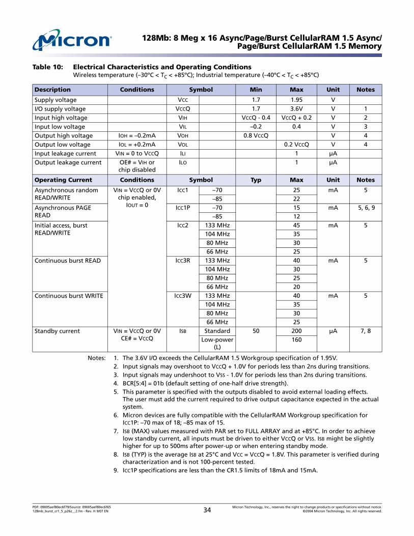
128Mb: 8 Meg x 16 Async/Page/Burst CellularRAM 1.5 Async/Page/Burst CellularRAM 1.5 Memory
Notes: 1. The 3.6V I/O exceeds the CellularRAM 1.5 Workgroup specification of 1.95V.2. Input signals may overshoot to VCCQ + 1.0V for periods less than 2ns during transitions.3. Input signals may undershoot to VSS - 1.0V for periods less than 2ns during transitions.4. BCR[5:4] = 01b (default setting of one-half drive strength).5. This parameter is specified with the outputs disabled to avoid external loading effects.
The user must add the current required to drive output capacitance expected in the actual system.
6. Micron devices are fully compatible with the CellularRAM Workgroup specification for ICC1P: –70 max of 18; –85 max of 15.
7. ISB (MAX) values measured with PAR set to FULL ARRAY and at +85°C. In order to achieve low standby current, all inputs must be driven to either VCCQ or VSS. ISB might be slightly higher for up to 500ms after power-up or when entering standby mode.
8. ISB (TYP) is the average ISB at 25°C and VCC = VCCQ = 1.8V. This parameter is verified during characterization and is not 100-percent tested.
9. ICC1P specifications are less than the CR1.5 limits of 18mA and 15mA.
Table 10: Electrical Characteristics and Operating ConditionsWireless temperature (–30ºC < TC < +85ºC); Industrial temperature (–40ºC < TC < +85ºC)
Description Conditions Symbol Min Max Unit Notes
Supply voltage VCC 1.7 1.95 V
I/O supply voltage VCCQ 1.7 3.6V V 1
Input high voltage VIH VCCQ - 0.4 VCCQ + 0.2 V 2
Input low voltage VIL –0.2 0.4 V 3
Output high voltage IOH = –0.2mA VOH 0.8 VCCQ V 4
Output low voltage IOL = +0.2mA VOL 0.2 VCCQ V 4
Input leakage current VIN = 0 to VCCQ ILI 1 µA
Output leakage current OE# = VIH or chip disabled
ILO 1 µA
Operating Current Conditions Symbol Typ Max Unit Notes
Asynchronous random READ/WRITE
VIN = VCCQ or 0Vchip enabled,
IOUT = 0
ICC1 –70 25 mA 5–85 22
Asynchronous PAGE READ
ICC1P –70 15 mA 5, 6, 9–85 12
Initial access, burst READ/WRITE
ICC2 133 MHz 45 mA 5104 MHz 3580 MHz 3066 MHz 25
Continuous burst READ ICC3R 133 MHz 40 mA 5104 MHz 3080 MHz 2566 MHz 20
Continuous burst WRITE ICC3W 133 MHz 40 mA 5104 MHz 3580 MHz 3066 MHz 25
Standby current VIN = VCCQ or 0V CE# = VCCQ
ISB Standard 50 200 µA 7, 8Low-power
(L)160
PDF: 09005aef80ec6f79/Source: 09005aef80ec6f65 Micron Technology, Inc., reserves the right to change products or specifications without notice.128mb_burst_cr1_5_p26z__2.fm - Rev. H 9/07 EN 34 ©2004 Micron Technology, Inc. All rights reserved.
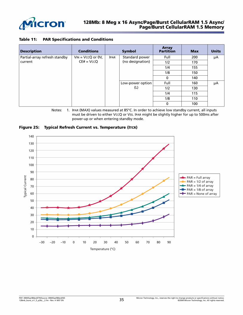
128Mb: 8 Meg x 16 Async/Page/Burst CellularRAM 1.5 Async/Page/Burst CellularRAM 1.5 Memory
Notes: 1. IPAR (MAX) values measured at 85°C. In order to achieve low standby current, all inputs must be driven to either VCCQ or VSS. IPAR might be slightly higher for up to 500ms after power-up or when entering standby mode.
Figure 25: Typical Refresh Current vs. Temperature (ITCR)
Table 11: PAR Specifications and Conditions
Description Conditions SymbolArray
Partition Max Units
Partial-array refresh standby current
VIN = VCCQ or 0V, CE# = VCCQ
IPAR Standard power(no designation)
Full 200 µA1/2 1701/4 1551/8 1500 140
Low-power option(L)
Full 160 µA1/2 1301/4 1151/8 1100 100
–30 –20 –10 0 10 20 30 40 50 60 70 80 90
Typ
ical
Cu
rren
t
Temperature (°C)
PAR = Full arrayPAR = 1/2 of arrayPAR = 1/4 of arrayPAR = 1/8 of arrayPAR = None of array
140
130
120
110
100
90
80
70
60
50
40
30
20
10
0
PDF: 09005aef80ec6f79/Source: 09005aef80ec6f65 Micron Technology, Inc., reserves the right to change products or specifications without notice.128mb_burst_cr1_5_p26z__2.fm - Rev. H 9/07 EN 35 ©2004 Micron Technology, Inc. All rights reserved.

128Mb: 8 Meg x 16 Async/Page/Burst CellularRAM 1.5 Async/Page/Burst CellularRAM 1.5 Memory
Figure 26: AC Input/Output Reference Waveform
Notes: 1. AC test inputs are driven at VCCQ for a logic 1 and VSSQ for a logic 0. Input rise and fall times (10 percent to 90 percent) <1.6ns.
2. Input timing begins at VCCQ/2. 3. Output timing ends at VCCQ/2.
Figure 27: AC Output Load Circuit
Notes: 1. All tests are performed with the outputs configured for default setting of half drive strength (BCR[5:4] = 01b).
Table 12: Deep Power-Down Specifications Typical (TYP) IZZ value applies across all operating temperatures and voltages
Description Conditions Symbol Typ Max Unit
Deep Power-Down VIN = VCCQ or 0V; VCC, VCCQ = 1.95V; +85°C
IZZ 3 10 µA
Table 13: Capacitance These parameters are verified in device characterization and are not 100-percent tested
Description Conditions Symbol Min Max Units
Input Capacitance TC = +25ºC; f = 1 MHz;VIN = 0V
CIN 2.0 6 pF
Input/Output Capacitance (DQ)
CIO 3.5 6 pF
OutputTest PointsInput1
VCCQ
VSSQ
VCCQ/23VCCQ/22
DUT VccQ/2
30pF
Test Point
50Ω
PDF: 09005aef80ec6f79/Source: 09005aef80ec6f65 Micron Technology, Inc., reserves the right to change products or specifications without notice.128mb_burst_cr1_5_p26z__2.fm - Rev. H 9/07 EN 36 ©2004 Micron Technology, Inc. All rights reserved.
128Mb: 8 Meg x 16 Async/Page/Burst CellularRAM 1.5 Async/Page/Burst CellularRAM 1.5 Memory
Timing Requirements
Notes: 1. Low-Z to High-Z timings are tested with the circuit shown in Figure 27 on page 36. The High-Z timings measure a 100mV transition from either VOH or VOL toward VCCQ/2.
2. High-Z to Low-Z timings are tested with the circuit shown in Figure 27 on page 36. The Low-Z timings measure a 100mV transition away from the High-Z (VCCQ/2) level toward either VOH or VOL.
3. Page mode enabled only.
Table 14: Asynchronous READ Cycle Timing RequirementsAll tests performed with outputs configured for default setting of one-half drive strength, (BCR[5:4] = 01b)
Parameter Symbol
70ns 85ns
Unit NotesMin Max Min Max
Address access time tAA 70 85 ns
ADV# access time tAADV 70 85 ns
Page access time tAPA 20 25 ns
Address hold from ADV# HIGH tAVH 2 2 ns
Address setup to ADV# HIGH tAVS 5 5 ns
LB#/UB# access time tBA 70 85 ns
LB#/UB# disable to DQ High-Z output tBHZ 8 8 ns 1
LB#/UB# enable to Low-Z output tBLZ 10 10 ns 2
Maximum CE# pulse width tCEM 4 4 µs 3
CE# LOW to WAIT valid tCEW 1 7.5 1 7.5 ns
Chip select access time tCO 70 85 ns
CE# LOW to ADV# HIGH tCVS 7 7 ns
Chip disable to DQ and WAIT High-Z output tHZ 8 8 ns 1
Chip enable to Low-Z output tLZ 10 10 ns 2
Output enable to valid output tOE 20 20 ns
Output hold from address change tOH 5 5 ns
Output disable to DQ High-Z output tOHZ 8 8 ns 1
Output enable to Low-Z output tOLZ 3 3 ns 2
Page READ cycle time tPC 20 25 ns
READ cycle time tRC 70 85 ns
ADV# pulse width LOW tVP 5 7 ns
PDF: 09005aef80ec6f79/Source: 09005aef80ec6f65 Micron Technology, Inc., reserves the right to change products or specifications without notice.128mb_burst_cr1_5_p26z__2.fm - Rev. H 9/07 EN 37 ©2004 Micron Technology, Inc. All rights reserved.
128Mb: 8 Meg x 16 Async/Page/Burst CellularRAM 1.5 Async/Page/Burst CellularRAM 1.5 Memory
Notes: 1. Values are valid for tCLK (MIN) with no refresh collision: LC= 4 for -7013; LC = 3 for -701,-708, and -856.
2. A refresh opportunity must be provided every tCEM. A refresh opportunity is satisfied by either of the following two conditions: a) clocked CE# HIGH, or b) CE# HIGH for longer than 15ns.
3. Low-Z to High-Z timings are tested with the circuit shown in Figure 27 on page 36. The High-Z timings measure a 100mV transition from either VOH or VOL toward VCCQ/2.
4. High-Z to Low-Z timings are tested with the circuit shown in Figure 27 on page 36. TheLow-Z timings measure a 100mV transition away from the High-Z (VCCQ/2) level toward either VOH or VOL.
Table 15: Burst READ Cycle Timing RequirementsAll tests performed with outputs configured for default setting of one-half drive strength (BCR[5:4] = 01b).
Parameter Symbol
-7013 (133 MHz)
-701 (104 MHz)
-708 (80 MHz)
-856(66 MHz)
Unit NotesMin Max Min Max Min Max Min Max
Address access time (fixed latency) tAA 70 70 70 85 ns
ADV# access time (fixed latency) tAADV 70 70 70 85 ns
Burst to READ access time (variable latency) tABA 35.5 35.9 46.5 55 ns 1
CLK to output delay
Variable LC = 4 Fixed LC = 8
tACLK 5.5 7 9 11 ns
All other LCs 7 7 9 11 ns
Address hold from ADV# HIGH (fixed latency)
tAVH 2 2 2 2 ns
Burst OE# LOW to output delay tBOE 20 20 20 20 ns
CE# HIGH between subsequent burst or mixed-mode operations
tCBPH 5 5 6 8 ns 2
Maximum CE# pulse width tCEM 4 4 4 4 µs 2
CE# LOW to WAIT valid tCEW 1 7.5 1 7.5 1 7.5 1 7.5 ns
CLK period tCLK 7.5 9.62 12.5 15 ns
Chip select access time (fixed latency) tCO 70 70 70 85 ns
CE# setup time to active CLK edge tCSP 2.5 3 4 5 ns
Hold time from active CLK Edge tHD 1.5 2 2 2 ns
Chip disable to DQ and WAIT High-Z output tHZ 7 8 8 8 ns 4
CLK rise or fall time tKHKL 1.2 1.6 1.8 2.0 ns
CLK to WAIT valid
Variable LC = 4 Fixed LC = 8 tKHTL
5.5 7 9 11 ns
All other LCs 7 7 9 11 ns
Output hold from CLK tKOH 2 2 2 2 ns
CLK HIGH or LOW time tKP 3 3 4 5 ns
Output disable to DQ High-Z output tOHZ 7 8 8 8 ns 3
Output enable to Low-Z output tOLZ 3 3 3 3 ns 4
Setup time to active CLK edge tSP 2 3 3 3 ns
PDF: 09005aef80ec6f79/Source: 09005aef80ec6f65 Micron Technology, Inc., reserves the right to change products or specifications without notice.128mb_burst_cr1_5_p26z__2.fm - Rev. H 9/07 EN 38 ©2004 Micron Technology, Inc. All rights reserved.
128Mb: 8 Meg x 16 Async/Page/Burst CellularRAM 1.5 Async/Page/Burst CellularRAM 1.5 Memory
Notes: 1. Low-Z to High-Z timings are tested with the circuit shown in Figure 27 on page 36. The High-Z timings measure a 100mV transition from either VOH or VOL toward VCCQ/2.
2. High-Z to Low-Z timings are tested with the circuit shown in Figure 27 on page 36. The Low-Z timings measure a 100mV transition away from the High-Z (VCCQ/2) level toward either VOH or VOL.
3. WE# LOW time must be limited to tCEM (4µs).
Table 16: Asynchronous WRITE Cycle Timing Requirements
Parameter Symbol
70ns 85ns
Unit NotesMin Max Min Max
Address and ADV# LOW setup time tAS 0 0 ns
Address HOLD from ADV# going HIGH tAVH 2 2 ns
Address setup to ADV# going HIGH tAVS 5 5 ns
Address valid to end of WRITE tAW 70 85 ns
LB#/UB# select to end of WRITE tBW 70 85 ns
CE# LOW to WAIT valid tCEW 1 7.5 1 7.5 ns
CE# HIGH between subsequent async operations tCPH 5 5 ns
CE# LOW to ADV# HIGH tCVS 7 7 ns
Chip enable to end of WRITE tCW 70 85 ns
Data HOLD from WRITE time tDH 0 0 ns
Data WRITE setup time tDW 20 20 ns
Chip disable to WAIT High-Z output tHZ 8 8 ns 1
Chip enable to Low-Z output tLZ 10 10 ns 2
End WRITE to Low-Z output tOW 5 5 ns 2
ADV# pulse width tVP 5 7 ns
ADV# setup to end of WRITE tVS 70 85 ns
WRITE cycle time tWC 70 85 ns
WRITE to DQ High-Z output tWHZ 8 8 ns 1
WRITE pulse width tWP 45 55 ns 3
WRITE pulse width HIGH tWPH 10 10 ns
WRITE recovery time tWR 0 0 ns
PDF: 09005aef80ec6f79/Source: 09005aef80ec6f65 Micron Technology, Inc., reserves the right to change products or specifications without notice.128mb_burst_cr1_5_p26z__2.fm - Rev. H 9/07 EN 39 ©2004 Micron Technology, Inc. All rights reserved.
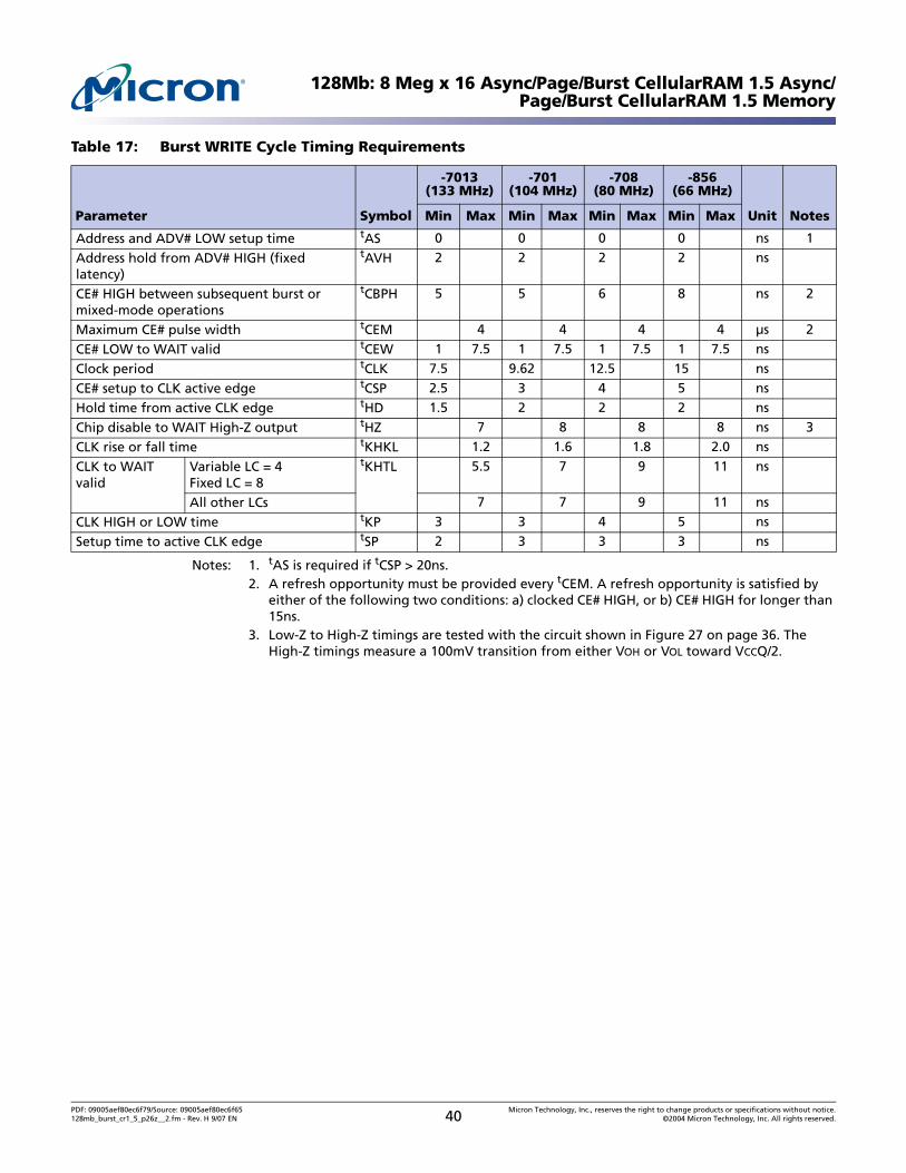
128Mb: 8 Meg x 16 Async/Page/Burst CellularRAM 1.5 Async/Page/Burst CellularRAM 1.5 Memory
.
Notes: 1. tAS is required if tCSP > 20ns.2. A refresh opportunity must be provided every tCEM. A refresh opportunity is satisfied by
either of the following two conditions: a) clocked CE# HIGH, or b) CE# HIGH for longer than 15ns.
3. Low-Z to High-Z timings are tested with the circuit shown in Figure 27 on page 36. The High-Z timings measure a 100mV transition from either VOH or VOL toward VCCQ/2.
Table 17: Burst WRITE Cycle Timing Requirements
Parameter Symbol
-7013 (133 MHz)
-701(104 MHz)
-708 (80 MHz)
-856(66 MHz)
Unit NotesMin Max Min Max Min Max Min Max
Address and ADV# LOW setup time tAS 0 0 0 0 ns 1
Address hold from ADV# HIGH (fixed latency)
tAVH 2 2 2 2 ns
CE# HIGH between subsequent burst or mixed-mode operations
tCBPH 5 5 6 8 ns 2
Maximum CE# pulse width tCEM 4 4 4 4 µs 2
CE# LOW to WAIT valid tCEW 1 7.5 1 7.5 1 7.5 1 7.5 ns
Clock period tCLK 7.5 9.62 12.5 15 ns
CE# setup to CLK active edge tCSP 2.5 3 4 5 ns
Hold time from active CLK edge tHD 1.5 2 2 2 ns
Chip disable to WAIT High-Z output tHZ 7 8 8 8 ns 3
CLK rise or fall time tKHKL 1.2 1.6 1.8 2.0 ns
CLK to WAIT valid
Variable LC = 4Fixed LC = 8
tKHTL 5.5 7 9 11 ns
All other LCs 7 7 9 11 ns
CLK HIGH or LOW time tKP 3 3 4 5 ns
Setup time to active CLK edge tSP 2 3 3 3 ns
PDF: 09005aef80ec6f79/Source: 09005aef80ec6f65 Micron Technology, Inc., reserves the right to change products or specifications without notice.128mb_burst_cr1_5_p26z__2.fm - Rev. H 9/07 EN 40 ©2004 Micron Technology, Inc. All rights reserved.
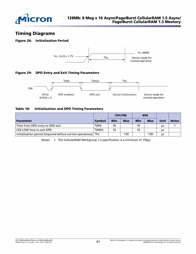
128Mb: 8 Meg x 16 Async/Page/Burst CellularRAM 1.5 Async/Page/Burst CellularRAM 1.5 Memory
Timing Diagrams
Figure 28: Initialization Period
Figure 29: DPD Entry and Exit Timing Parameters
Notes: 1. The CellularRAM Workgroup 1.5 specification is a minimum of 150µs.
Table 18: Initialization and DPD Timing Parameters
Parameter Symbol
-701/708 -856
Unit NotesMin Max Min Max
Time from DPD entry to DPD exit tDPD 10 10 µs 1
CE# LOW time to exit DPD tDPDX 10 10 µs
Initialization period (required before normal operations) tPU 150 150 µs
tPUVCC, VCCQ = 1.7V
VCC (MIN)
Device ready fornormal operation
CE#
DPD enabledWrite RCR[4] = 0
DPD exit Device initialization Device ready fornormal operation
tDPD tDPDX tPU
PDF: 09005aef80ec6f79/Source: 09005aef80ec6f65 Micron Technology, Inc., reserves the right to change products or specifications without notice.128mb_burst_cr1_5_p26z__2.fm - Rev. H 9/07 EN 41 ©2004 Micron Technology, Inc. All rights reserved.

128Mb: 8 Meg x 16 Async/Page/Burst CellularRAM 1.5 Async/Page/Burst CellularRAM 1.5 Memory
Figure 30: Asynchronous READ
VIH
VIL
VIH
VIL
VIH
VIL
VIH
VIL
VIH
VIL
VIH
VIL
VOH
VOL
VOH
VOL
A[22:0]
ADV#
CE#
LB#/UB#
OE#
WE#
WAIT
DQ[15:0]
Valid Address
tAA
tHZ
tBA
High-Z High-Z
tRC
tCOtBHZ
tOHZ
tHZ
tOE
tCEW
Valid OutputHigh-Z
UndefinedDon’t Care
tBLZtLZ
tOLZ
PDF: 09005aef80ec6f79/Source: 09005aef80ec6f65 Micron Technology, Inc., reserves the right to change products or specifications without notice.128mb_burst_cr1_5_p26z__2.fm - Rev. H 9/07 EN 42 ©2004 Micron Technology, Inc. All rights reserved.
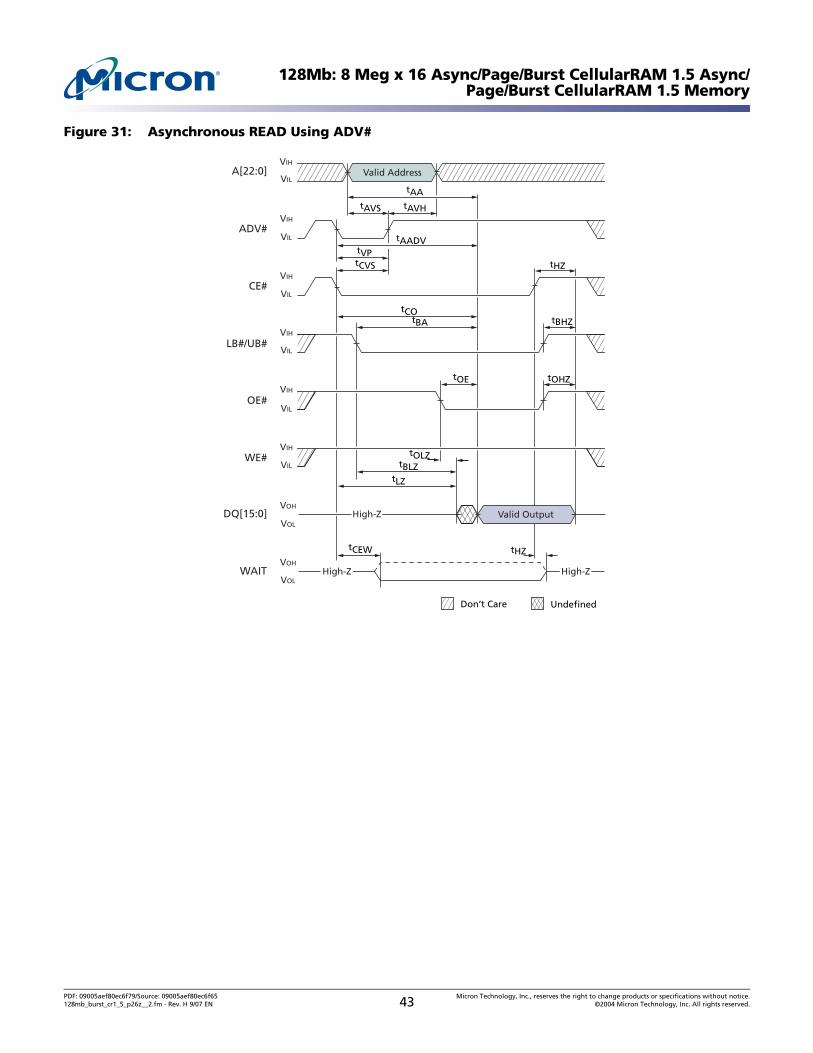
128Mb: 8 Meg x 16 Async/Page/Burst CellularRAM 1.5 Async/Page/Burst CellularRAM 1.5 Memory
Figure 31: Asynchronous READ Using ADV#
A[22:0]
ADV#
CE#
LB#/UB#
OE#
WE#
WAIT
DQ[15:0]
Valid Address
tAADV
tAA
tVPtHZ
tBA
High-Z High-Z
tCVS
tCO
tBLZ
tBHZ
tOHZ
tHZ
tLZ
tOE
tOLZ
Valid Output
tAVHtAVS
High-Z
UndefinedDon’t Care
tCEW
VIH
VIL
VIH
VIL
VIH
VIL
VIH
VIL
VIH
VIL
VIH
VIL
VOH
VOL
VOH
VOL
PDF: 09005aef80ec6f79/Source: 09005aef80ec6f65 Micron Technology, Inc., reserves the right to change products or specifications without notice.128mb_burst_cr1_5_p26z__2.fm - Rev. H 9/07 EN 43 ©2004 Micron Technology, Inc. All rights reserved.

128Mb: 8 Meg x 16 Async/Page/Burst CellularRAM 1.5 Async/Page/Burst CellularRAM 1.5 Memory
Figure 32: Page Mode READ
A[3:0]
ADV#
CE#
LB#/UB#
OE#
WE#
WAIT
DQ[15:0]
Valid Address
tAA
tHZ
tBA
High-Z High-Z
tCO
tCEM
tBLZ
tBHZ
tOHZ
tHZ
tLZ
tOE
tOLZ
tCEW
High-Z
Undefined Don’t Care
A[22:4] Valid Address
Valid Address
Valid Address
Valid Address
tRC
Valid Output
tAPA
tPC
VIH
VIL
VIH
VIL
VIH
VIL
VIH
VIL
VIH
VIL
VIH
VIL
VIH
VIL
VOH
VOL
VOH
VOL
tOH
Valid Output
Valid Output
Valid Output
PDF: 09005aef80ec6f79/Source: 09005aef80ec6f65 Micron Technology, Inc., reserves the right to change products or specifications without notice.128mb_burst_cr1_5_p26z__2.fm - Rev. H 9/07 EN 44 ©2004 Micron Technology, Inc. All rights reserved.

128Mb: 8 Meg x 16 Async/Page/Burst CellularRAM 1.5 Async/Page/Burst CellularRAM 1.5 Memory
Figure 33: Single-Access Burst READ Operation – Variable Latency
Notes: 1. Non-default BCR settings: Latency code two (three clocks); WAIT active LOW; WAIT asserted during delay.
A[22:0]VIH
VIL
ADV#VIH
VIL
CE#VIH
VIL
OE#VIH
VIL
WE#VIH
VIL
WAIT
DQ[15:0]
VOH
VOL
CLKVIH
VIL
VOH
VOL
tSP
tCLK
tCEW
tHD
tABA
tHD
ValidOutput
ValidAddress
High-Z
tKOH
tOHZ
tSP
LB#/UB#VIH
VIL
tCSP
tCEM
High-Z
tOLZtHD
tHDtSP
tHZ
tKP tKP
tKHKL
tHD
tSP
UndefinedDon’t CareREAD Burst Identified(WE# = HIGH)
tKHTL
tBOE
High-Z
tACLK
PDF: 09005aef80ec6f79/Source: 09005aef80ec6f65 Micron Technology, Inc., reserves the right to change products or specifications without notice.128mb_burst_cr1_5_p26z__2.fm - Rev. H 9/07 EN 45 ©2004 Micron Technology, Inc. All rights reserved.
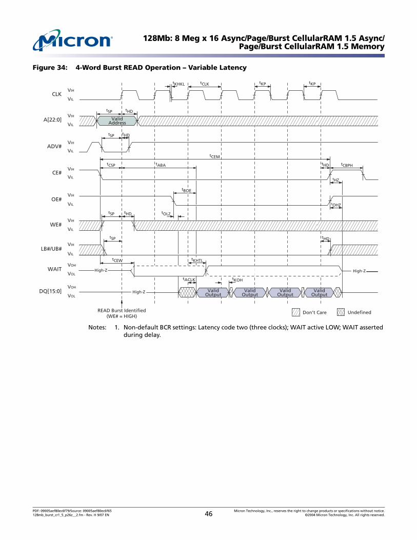
128Mb: 8 Meg x 16 Async/Page/Burst CellularRAM 1.5 Async/Page/Burst CellularRAM 1.5 Memory
Figure 34: 4-Word Burst READ Operation – Variable Latency
Notes: 1. Non-default BCR settings: Latency code two (three clocks); WAIT active LOW; WAIT asserted during delay.
A[22:0] VIH
VIL
ADV# VIH
VIL
CE# VIH
VIL
OE# VIH
VIL
WE# VIH
VIL
WAIT
DQ[15:0]
VOH
VOL
CLK VIH
VIL
VOH
VOL
tSP
tCLK tKHKL
tHD
tABA
Valid Address
High-Z
tKOH
tHZ
tHD
tSP
LB#/UB# VIH
VIL
High-Z
tOLZ
High-Z
tCBPH tCSP
tCEM
tSP tHD
tSP tHD
tOHZ
tHD
tKP tKP
Undefined Don’t Care READ Burst Identified (WE# = HIGH)
tCEW
tACLK
tKHTL
Valid Output
Valid Output
Valid Output
Valid Output
tBOE
PDF: 09005aef80ec6f79/Source: 09005aef80ec6f65 Micron Technology, Inc., reserves the right to change products or specifications without notice.128mb_burst_cr1_5_p26z__2.fm - Rev. H 9/07 EN 46 ©2004 Micron Technology, Inc. All rights reserved.
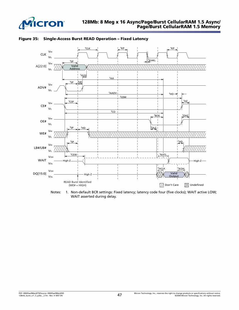
128Mb: 8 Meg x 16 Async/Page/Burst CellularRAM 1.5 Async/Page/Burst CellularRAM 1.5 Memory
Figure 35: Single-Access Burst READ Operation – Fixed Latency
Notes: 1. Non-default BCR settings: Fixed latency; latency code four (five clocks); WAIT active LOW; WAIT asserted during delay.
A[22:0]VIH
VIL
ADV#VIH
VIL
CE#VIH
VIL
OE#VIH
VIL
WE#VIH
VIL
WAIT
DQ[15:0]
VOH
VOL
CLKVIH
VIL
VOH
VOL
tCLK
tCEW
tAVH
tCO
tAADV
tAAtHD
ValidOutput
ValidAddress
High-Z
tKOH
tOHZ
tSP
tSP
LB#/UB#VIH
VIL
tCSP
tCEM
High-Z
tOLZtHD
tHDtSP
tHZ
tKP tKP
tKHKL
tHD
tSP
UndefinedDon’t CareREAD Burst Identified
(WE# = HIGH)
tKHTL
tBOE
High-Z
tACLK
PDF: 09005aef80ec6f79/Source: 09005aef80ec6f65 Micron Technology, Inc., reserves the right to change products or specifications without notice.128mb_burst_cr1_5_p26z__2.fm - Rev. H 9/07 EN 47 ©2004 Micron Technology, Inc. All rights reserved.

128Mb: 8 Meg x 16 Async/Page/Burst CellularRAM 1.5 Async/Page/Burst CellularRAM 1.5 Memory
Figure 36: 4-Word Burst READ Operation – Fixed Latency
Notes: 1. Non-default BCR settings: Fixed latency; latency code two (three clocks); WAIT active LOW; WAIT asserted during delay.
A[22:0]VIH
VIL
ADV#VIH
VIL
CE#VIH
VIL
OE#VIH
VIL
WE#VIH
VIL
WAIT
DQ[15:0]
VOH
VOL
CLKVIH
VIL
VOH
VOL
tAVH
tCLKtKHKL
tCO
tAADV
tAA
High-Z
tKOH
tHZ
tHD
tSP
tSP
LB#/UB#VIH
VIL
High-Z
tOLZ
High-Z
tCBPHtCSP
tCEM
tSP tHD
tSP tHD
tOHZ
tHD
tKP tKP
UndefinedDon’t CareREAD Burst Identified
(WE# = HIGH)
tCEW tKHTL
tACLK
ValidOutput
ValidOutput
ValidOutput
ValidOutput
tBOE
ValidAddress
PDF: 09005aef80ec6f79/Source: 09005aef80ec6f65 Micron Technology, Inc., reserves the right to change products or specifications without notice.128mb_burst_cr1_5_p26z__2.fm - Rev. H 9/07 EN 48 ©2004 Micron Technology, Inc. All rights reserved.
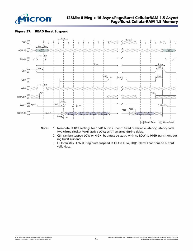
128Mb: 8 Meg x 16 Async/Page/Burst CellularRAM 1.5 Async/Page/Burst CellularRAM 1.5 Memory
Figure 37: READ Burst Suspend
Notes: 1. Non-default BCR settings for READ burst suspend: Fixed or variable latency; latency code two (three clocks); WAIT active LOW; WAIT asserted during delay.
2. CLK can be stopped LOW or HIGH, but must be static, with no LOW-to-HIGH transitions dur-ing burst suspend.
3. OE# can stay LOW during burst suspend. If OE# is LOW, DQ[15:0] will continue to output valid data.
A[22:0]VIH
VIL
ADV#VIH
VIL
CE#VIH
VIL
OE# VIH
VIL
WE#VIH
VIL
WAIT
DQ[15:0]
VOH
VOL
CLKVIH
VIL
VOH
VOL
tSP tHD
High-Z
tOLZ
tACLK
LB#/UB#VIH
VIL
tCLK
tSP
tCSP
tSP tHD
tHD
tSP tHD
tKOH
ValidOutput
ValidOutput
UndefinedDon’t Care
ValidAddress
High-Z
tCBPHtCEMtHZ
tOHZ
ValidOutput
ValidOutput
ValidOutput
ValidOutput
tBOE
tOHZ
tBOEtOLZ
ValidAddress
Note 3
Note 2
High-Z
PDF: 09005aef80ec6f79/Source: 09005aef80ec6f65 Micron Technology, Inc., reserves the right to change products or specifications without notice.128mb_burst_cr1_5_p26z__2.fm - Rev. H 9/07 EN 49 ©2004 Micron Technology, Inc. All rights reserved.
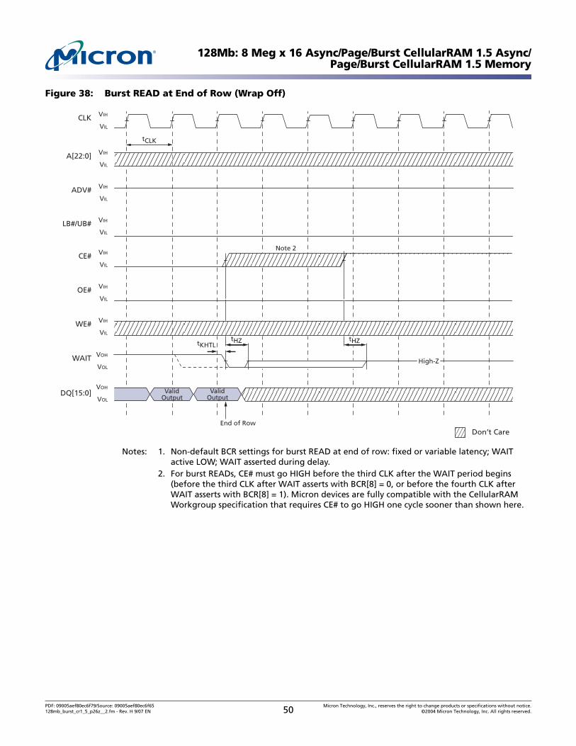
128Mb: 8 Meg x 16 Async/Page/Burst CellularRAM 1.5 Async/Page/Burst CellularRAM 1.5 Memory
Figure 38: Burst READ at End of Row (Wrap Off)
Notes: 1. Non-default BCR settings for burst READ at end of row: fixed or variable latency; WAIT active LOW; WAIT asserted during delay.
2. For burst READs, CE# must go HIGH before the third CLK after the WAIT period begins (before the third CLK after WAIT asserts with BCR[8] = 0, or before the fourth CLK after WAIT asserts with BCR[8] = 1). Micron devices are fully compatible with the CellularRAM Workgroup specification that requires CE# to go HIGH one cycle sooner than shown here.
A[22:0] VIH
VIL
ADV# VIH
VIL
CE# VIH
VIL
OE# VIH
VIL
WE# VIH
VIL
WAIT
DQ[15:0]
VOH
VOL
CLK VIH
VIL
VOH
VOL
tKHTL tHZ
tCLK
LB#/UB# VIH
VIL
Valid Output
Don’t Care
Valid Output
End of Row
tHZ
High-Z
Note 2
PDF: 09005aef80ec6f79/Source: 09005aef80ec6f65 Micron Technology, Inc., reserves the right to change products or specifications without notice.128mb_burst_cr1_5_p26z__2.fm - Rev. H 9/07 EN 50 ©2004 Micron Technology, Inc. All rights reserved.
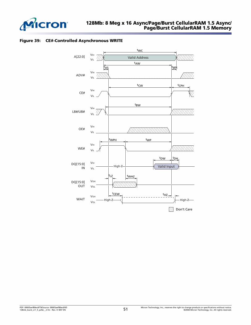
128Mb: 8 Meg x 16 Async/Page/Burst CellularRAM 1.5 Async/Page/Burst CellularRAM 1.5 Memory
Figure 39: CE#-Controlled Asynchronous WRITE
A[22:0]
ADV#
CE#
LB#/UB#
OE#
WE#
WAIT
DQ[15:0]IN
Valid Address
High-Z High-Z
tWC
tCEW tHZ
Valid Input
tAW
Don’t Care
tWR
tCW tCPH
tDW
DQ[15:0] OUT
tWHZ
tBW
tLZ
tDH
tAS
tWPtWPH
VIH
VIL
VIH
VIL
VIH
VIL
VIH
VIL
VIH
VIL
VIH
VIL
VIH
VIL
VOH
VOL
VOH
VOL
High-Z
PDF: 09005aef80ec6f79/Source: 09005aef80ec6f65 Micron Technology, Inc., reserves the right to change products or specifications without notice.128mb_burst_cr1_5_p26z__2.fm - Rev. H 9/07 EN 51 ©2004 Micron Technology, Inc. All rights reserved.

128Mb: 8 Meg x 16 Async/Page/Burst CellularRAM 1.5 Async/Page/Burst CellularRAM 1.5 Memory
Figure 40: LB#/UB#-Controlled Asynchronous WRITE
VIH
VIL
VIH
VIL
VIH
VIL
VIH
VIL
VIH
VIL
VIH
VIL
VOH
VOL
A[22:0]
ADV#
CE#
LB#/UB#
OE#
WE#
WAIT
DQ[15:0] IN
VIH
VIL
Valid Address
High-Z
tWC
tCEW tHZ
Valid Input
tAW
Don’t Care
tWR
tCW
tDW
DQ[15:0] OUT
VOH
VOL
tWHZ
tBW
tLZ
tDH
tAS
tWP tWPH
High-Z
High-Z
PDF: 09005aef80ec6f79/Source: 09005aef80ec6f65 Micron Technology, Inc., reserves the right to change products or specifications without notice.128mb_burst_cr1_5_p26z__2.fm - Rev. H 9/07 EN 52 ©2004 Micron Technology, Inc. All rights reserved.
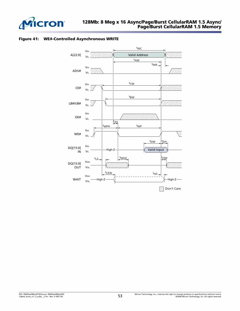
128Mb: 8 Meg x 16 Async/Page/Burst CellularRAM 1.5 Async/Page/Burst CellularRAM 1.5 Memory
Figure 41: WE#-Controlled Asynchronous WRITE
VIH
VIL
VIH
VIL
VIH
VIL
VIH
VIL
VIH
VIL
VIH
VIL
VOH
VOL
A[22:0]
ADV#
CE#
LB#/UB#
OE#
WE#
WAIT
DQ[15:0] IN
VIH
VIL
Valid Address
tWC
tCEW tHZ
Valid Input
tAW
Don’t Care
tWR
tDW
DQ[15:0] OUT
VOH
VOL
tWHZ
tBW
tCW
tLZ
tWP
tDH
tOW
tAS tWPH
High-Z
High-Z
High-Z
PDF: 09005aef80ec6f79/Source: 09005aef80ec6f65 Micron Technology, Inc., reserves the right to change products or specifications without notice.128mb_burst_cr1_5_p26z__2.fm - Rev. H 9/07 EN 53 ©2004 Micron Technology, Inc. All rights reserved.
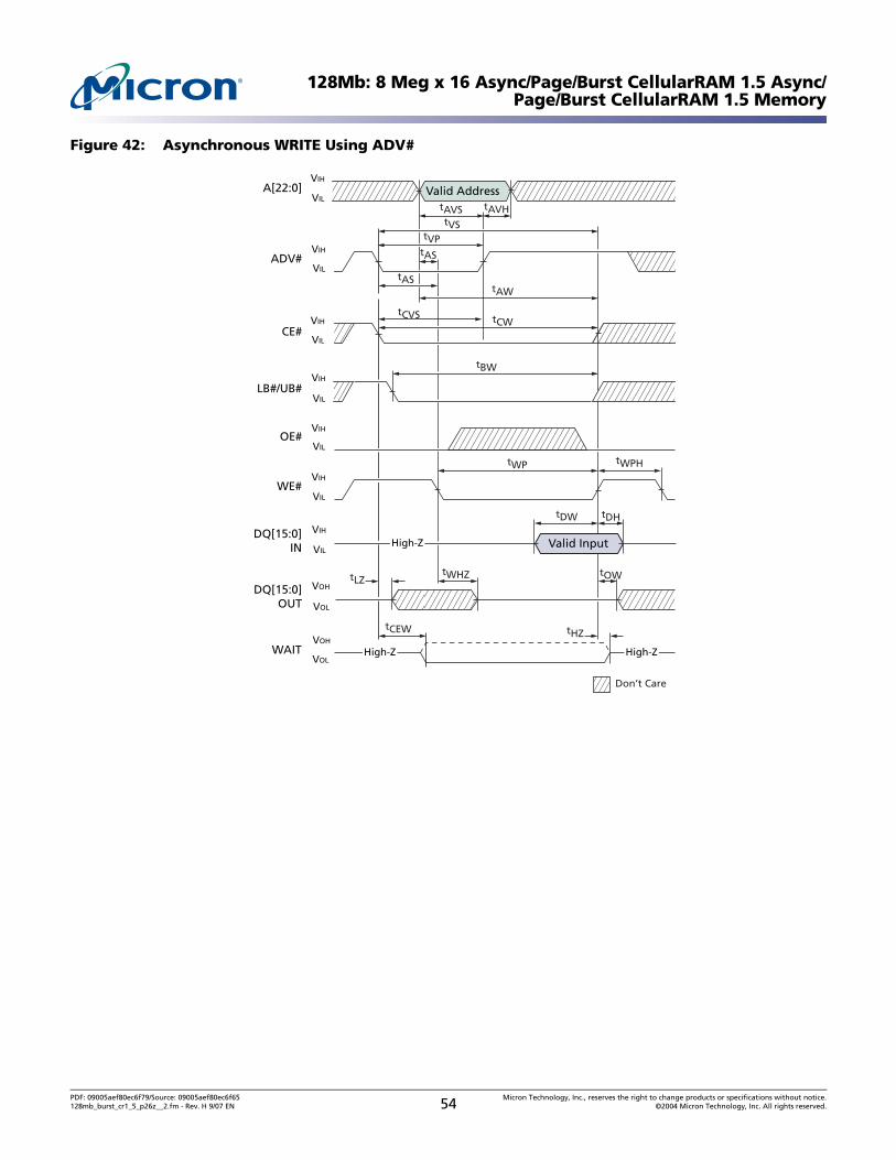
128Mb: 8 Meg x 16 Async/Page/Burst CellularRAM 1.5 Async/Page/Burst CellularRAM 1.5 Memory
Figure 42: Asynchronous WRITE Using ADV#
VIH
VIL
VIH
VIL
VIH
VIL
VIH
VIL
VIH
VIL
VIH
VIL
VOH
VOL
A[22:0]
ADV#
CE#
LB#/UB#
OE#
WE#
WAIT
DQ[15:0] IN
VIH
VIL
Valid Address
High-Z High-Z
tCEW tHZ
Valid Input
tVS
Don’t Care
tCW
tDW
DQ[15:0] OUT
VOH
VOL
tWHZ
tBW
tLZ
tWP
tDH
tOW
tAS
tWPH
tAS
tAVH tAVS
tVP
tAW
High-Z
tCVS
PDF: 09005aef80ec6f79/Source: 09005aef80ec6f65 Micron Technology, Inc., reserves the right to change products or specifications without notice.128mb_burst_cr1_5_p26z__2.fm - Rev. H 9/07 EN 54 ©2004 Micron Technology, Inc. All rights reserved.
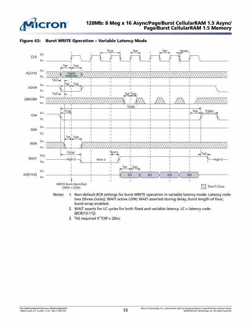
128Mb: 8 Meg x 16 Async/Page/Burst CellularRAM 1.5 Async/Page/Burst CellularRAM 1.5 Memory
Figure 43: Burst WRITE Operation – Variable Latency Mode
Notes: 1. Non-default BCR settings for burst WRITE operation in variable latency mode: Latency code two (three clocks); WAIT active LOW; WAIT asserted during delay; burst length of four; burst-wrap enabled.
2. WAIT asserts for LC cycles for both fixed and variable latency. LC = latency code (BCR[13:11]).
3. tAS required if tCSP > 20ns.
A[22:0] VIH
VIL
ADV# VIH
VIL
CE# VIH
VIL
OE# VIH
VIL
WE# VIH
VIL
WAIT
DQ[15:0]
VOH
VOL
CLK VIH
VIL
VIH
VIL
tCLK tKP
tSP
tAS3
tCSP
D0 D3 D2 D1
Valid Address
tHD tSP
tHD tSP
tHD
tHD
tSP
High-Z High-Z
LB#/UB# VIH
VIL
tSP tHD
tHD
Don’t Care WRITE Burst Identified
(WE# = LOW)
tCBPH
tKHTL
tAS3
tHZ tCEW
tKP tKHKL
Note 2
tCEM
PDF: 09005aef80ec6f79/Source: 09005aef80ec6f65 Micron Technology, Inc., reserves the right to change products or specifications without notice.128mb_burst_cr1_5_p26z__2.fm - Rev. H 9/07 EN 55 ©2004 Micron Technology, Inc. All rights reserved.
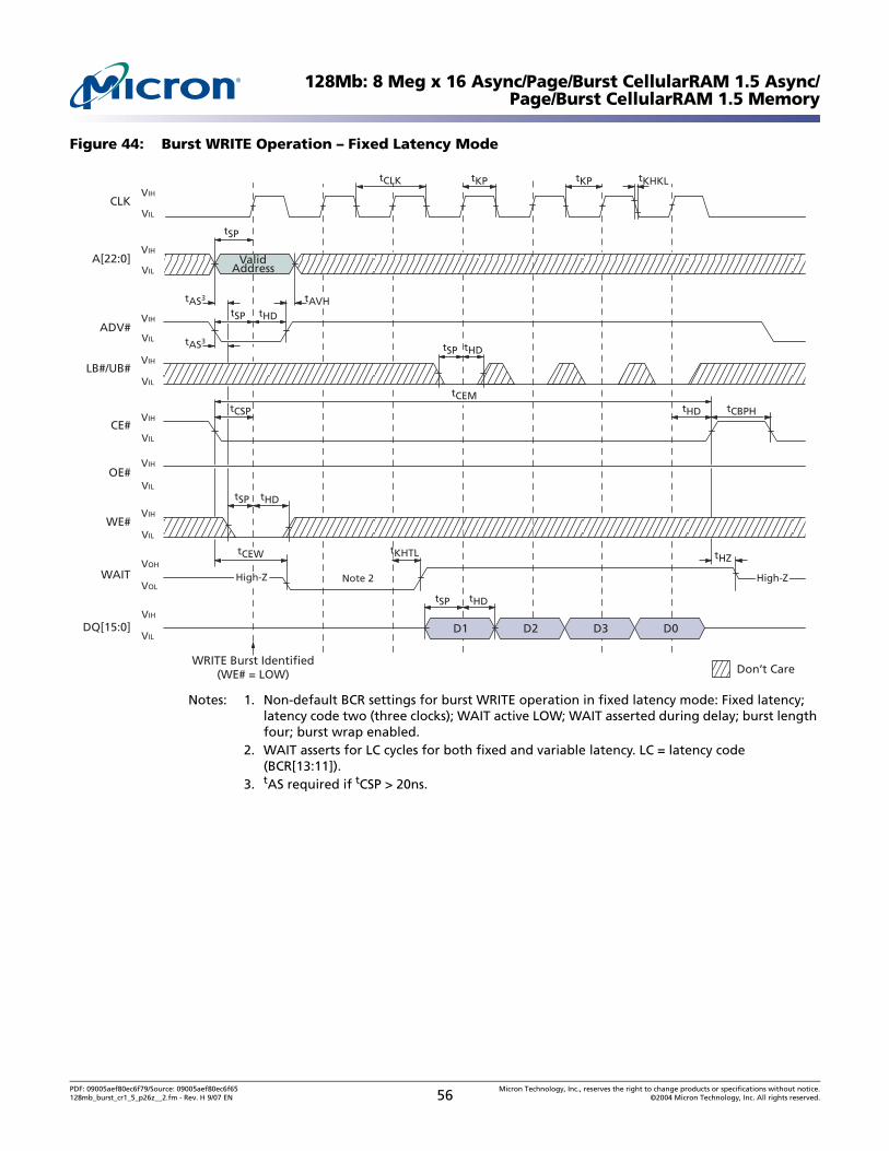
128Mb: 8 Meg x 16 Async/Page/Burst CellularRAM 1.5 Async/Page/Burst CellularRAM 1.5 Memory
Figure 44: Burst WRITE Operation – Fixed Latency Mode
Notes: 1. Non-default BCR settings for burst WRITE operation in fixed latency mode: Fixed latency; latency code two (three clocks); WAIT active LOW; WAIT asserted during delay; burst length four; burst wrap enabled.
2. WAIT asserts for LC cycles for both fixed and variable latency. LC = latency code (BCR[13:11]).
3. tAS required if tCSP > 20ns.
A[22:0] VIH
VIL
ADV# VIH
VIL
CE# VIH
VIL
OE# VIH
VIL
WE# VIH
VIL
WAIT
DQ[15:0]
VOH
VOL
CLK VIH
VIL
VIH
VIL
tCLK tKP
tSP
tAS3
tCSP
D0 D3 D2 D1
Valid Address
tHD tSP
tHD tSP
tHD
tSP
High-Z High-Z
LB#/UB# VIH
VIL
tSP tHD
tHD
Don’t Care WRITE Burst Identified
(WE# = LOW)
tCBPH
tKHTL
tAS3
tHZ tCEW
tKP tKHKL
Note 2
tCEM
tAVH
PDF: 09005aef80ec6f79/Source: 09005aef80ec6f65 Micron Technology, Inc., reserves the right to change products or specifications without notice.128mb_burst_cr1_5_p26z__2.fm - Rev. H 9/07 EN 56 ©2004 Micron Technology, Inc. All rights reserved.

128Mb: 8 Meg x 16 Async/Page/Burst CellularRAM 1.5 Async/Page/Burst CellularRAM 1.5 Memory
Figure 45: Burst WRITE at End of Row (Wrap Off)
Notes: 1. Non-default BCR settings for burst WRITE at end of row: fixed or variable latency; WAIT active LOW; WAIT asserted during delay.
2. For burst WRITEs, CE# must go HIGH before the third CLK after the WAIT period begins (before the third CLK after WAIT asserts with BCR[8] = 0, or before the fourth CLK after WAIT asserts with BCR[8] = 1).
3. Devices from different CellularRAM vendors can assert WAIT so that the end-of-row data is input one cycle before the WAIT period begins (as shown, solid line), or the same cycle that asserts WAIT. This difference in behavior will not be noticed by controllers that monitor WAIT, or that use WAIT to abort on an end-of-row condition.
4. Micron devices are fully compatible with the CellularRAM Workgroup specification that requires CE# to go HIGH one cycle sooner than shown here.
A[22:0] VIH
VIL
ADV# VIH
VIL
CE# VIH
VIL
OE#
VIH
VIL WE#
VIH
VIL
WAIT
DQ[15:0]
VOH
VOL
CLK VIH
VIL
VIH
VIL
tKHTL tHZ tHZ
tCLK
tSP tHD
End of row (A[6:0] = 7Fh)
Valid Input Valid Input
Don’t Care
VIH
VIL
LB#/UB#
High-Z
Note 2
Note 3
PDF: 09005aef80ec6f79/Source: 09005aef80ec6f65 Micron Technology, Inc., reserves the right to change products or specifications without notice.128mb_burst_cr1_5_p26z__2.fm - Rev. H 9/07 EN 57 ©2004 Micron Technology, Inc. All rights reserved.

128Mb: 8 Meg x 16 Async/Page/Burst CellularRAM 1.5 Async/Page/Burst CellularRAM 1.5 Memory
Figure 46: Burst WRITE Followed by Burst READ
Notes: 1. Non-default BCR settings for burst WRITE followed by burst READ: Fixed or variable latency; latency code two (three clocks); WAIT active LOW; WAIT asserted during delay.
2. A refresh opportunity must be provided every tCEM. A refresh opportunity is satisfied by either of the following two conditions: a) clocked CE# HIGH, or b) CE# HIGH for longer than 15ns. CE# can stay LOW between burst READ and burst WRITE operations, but CE# must not remain LOW longer than tCEM. See burst interrupt diagrams (Figures 47 through 49, on pages 59 through 61) for cases where CE# stays LOW between bursts.
A[22:0] VIH
VIL
ADV# VIH
VIL
CE# VIH
VIL
OE# VIH
VIL
WE# VIH
VIL
WAIT
DQ[15:0] IN/OUT
VOH
VOL
CLK VIH
VIL
VIH
VIL
tCLK
tSP
tSP
tCSP
D3 D2 D1 D0
Valid Address
tHD tSP
tHD tSP
tSP tHD
Valid Address
tCSP tOHZ
tKOH tACLK Valid
Output Valid
Output Valid
Output Valid
Output High-Z High-Z VOH
VOL
LB#/UB# VIH
VIL
tHD
tSP tHD
tSP tHD
tHD
High-Z
Undefined Don’t Care
tBOE
tCBPH
High-Z
tHD tHD tSP
Note 2
PDF: 09005aef80ec6f79/Source: 09005aef80ec6f65 Micron Technology, Inc., reserves the right to change products or specifications without notice.128mb_burst_cr1_5_p26z__2.fm - Rev. H 9/07 EN 58 ©2004 Micron Technology, Inc. All rights reserved.
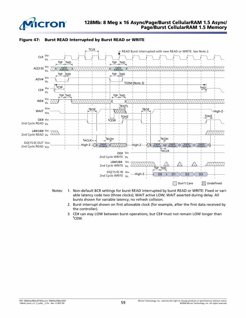
128Mb: 8 Meg x 16 Async/Page/Burst CellularRAM 1.5 Async/Page/Burst CellularRAM 1.5 Memory
Figure 47: Burst READ Interrupted by Burst READ or WRITE
Notes: 1. Non-default BCR settings for burst READ interrupted by burst READ or WRITE: Fixed or vari-able latency code two (three clocks); WAIT active LOW; WAIT asserted during delay. All bursts shown for variable latency; no refresh collision.
2. Burst interrupt shown on first allowable clock (for example, after the first data received by the controller).
3. CE# can stay LOW between burst operations, but CE# must not remain LOW longer than tCEM.
A[22:0] VIH
VIL
ADV# VIH
VIL
CE#VIH
VIL
OE#2nd Cycle READ
VIH
VIL
OE#2nd Cycle WRITE
VIH
VIL
WE#VIH
VIL
WAIT
DQ[15:0] OUT2nd Cycle READ
VOH
VOL
CLK VIH
VIL
DQ[15:0] IN2nd Cycle WRITE
VIH
VIL
tHDtSP
tSP tHD
tCLK
tOHZ
tKOH
tACLK
ValidOutput
ValidOutput
ValidOutput
ValidOutput
LB#/UB#2nd Cycle READ
VIH
VIL
LB#/UB# 2nd Cycle WRITE
VIH
VIL
tSP tHD
UndefinedDon’t Care
tHDtSP
tCSP
tSP tHD
ValidAddress
tOHZ
tKOHtACLKValid
OutputHigh-Z
tBOE
tCEW
tSP tHD
tHDtSP
VOH
VOL
tBOE
D2 D3D1D0
High-Z
tCEM (Note 3)
ValidAddress
READ Burst interrupted with new READ or WRITE. See Note 2.
High-Z
tKHTL
tHD
High-Z
PDF: 09005aef80ec6f79/Source: 09005aef80ec6f65 Micron Technology, Inc., reserves the right to change products or specifications without notice.128mb_burst_cr1_5_p26z__2.fm - Rev. H 9/07 EN 59 ©2004 Micron Technology, Inc. All rights reserved.

128Mb: 8 Meg x 16 Async/Page/Burst CellularRAM 1.5 Async/Page/Burst CellularRAM 1.5 Memory
Figure 48: Burst WRITE Interrupted by Burst WRITE or READ – Variable Latency Mode
Notes: 1. Non-default BCR settings for burst WRITE interrupted by burst WRITE or READ in variable latency mode: Variable latency; latency code two (three clocks); WAIT active LOW; WAIT asserted during delay. All bursts shown for variable latency; no refresh collision.
2. Burst interrupt shown on first allowable clock (i.e., after first data word written).3. CE# can stay LOW between burst operations, but CE# must not remain LOW longer than
tCEM.
A[22:0] VIH
VIL
ADV# VIH
VIL
CE# VIH
VIL
OE# 2nd Cycle WRITE
VIH
VIL
OE# 2nd Cycle READ
VIH
VIL
WE# VIH
VIL
WAIT
DQ[15:0] IN 2nd Cycle WRITE
DQ[15:0] OUT 2nd Cycle READ
VOH
VOL
CLK VIH
VIL
VIH
VIL
tCLK
tSP
tSP
tCSP
D0
Valid Address
tHD tSP
tHD tSP
tSP tHD
VALID ADDRESS
tHD
High-Z
LB#/UB# 2nd Cycle WRITE
LB#/UB# 2nd Cycle READ
VIH
VIL
VIH
VIL
tHD
tSP tHD
tKHTL
tSP tHD
UndefinedDon’t Care
D2 D3 D1 D0
tHD tSP
tHD tHD tSP
tOHZ tBOE
tSP tHD
tKOH tACLK Valid
Output Valid
Output Valid
Output Valid
Output High-Z VOH
VOL
VOH
VOL
WRITE Burst interrupted with new WRITE or READ. See Note 2.
Valid Address
tCEM (Note 3)
tCEW High-Z High-Z
PDF: 09005aef80ec6f79/Source: 09005aef80ec6f65 Micron Technology, Inc., reserves the right to change products or specifications without notice.128mb_burst_cr1_5_p26z__2.fm - Rev. H 9/07 EN 60 ©2004 Micron Technology, Inc. All rights reserved.

128Mb: 8 Meg x 16 Async/Page/Burst CellularRAM 1.5 Async/Page/Burst CellularRAM 1.5 Memory
Figure 49: Burst WRITE Interrupted by Burst WRITE or READ – Fixed Latency Mode
Notes: 1. Non-default BCR settings for burst WRITE interrupted by burst WRITE or READ in fixed latency mode: Fixed latency; latency code two (three clocks); WAIT active LOW; WAIT asserted during delay.
2. Burst interrupt shown on first allowable clock (i.e., after first data word written).3. CE# can stay LOW between burst operations, but CE# must not remain LOW longer than
tCEM.
A[22:0] VIH
VIL
ADV# VIH
VIL
CE# VIH
VIL
OE# 2nd Cycle WRITE
VIH
VIL
OE# 2nd Cycle READ
VIH
VIL
WE# VIH
VIL
WAIT
DQ[15:0] IN 2nd Cycle WRITE
DQ[15:0] OUT 2nd Cycle READ
VOH
VOL
CLK VIH
VIL
VIH
VIL
tCLK
tSP
tSP
tCSP
D0
Valid Address
tHD tSP
tHD tSP
tSP
tSP
tHD
High-Z
LB#/UB# 2nd Cycle WRITE
LB#/UB# 2nd Cycle READ
VIH
VIL
VIH
VIL
tSP tHD
tSP tHD
Undefined Don’t Care
tHD
D2 D3 D1 D0
tHD tSP
tHD tSP
tOHZ tBOE
tKOH
tACLK
Valid Output
Valid Output
Valid Output
Valid Output High-Z
VOH
VOL
VOH
VOL
tKHTL
WRITE Burst interrupted with new WRITE or READ. See Note 2.
Valid Address
tCEM (Note 3)
tAVH tAVH tHD
tCEW High-Z High-Z
PDF: 09005aef80ec6f79/Source: 09005aef80ec6f65 Micron Technology, Inc., reserves the right to change products or specifications without notice.128mb_burst_cr1_5_p26z__2.fm - Rev. H 9/07 EN 61 ©2004 Micron Technology, Inc. All rights reserved.
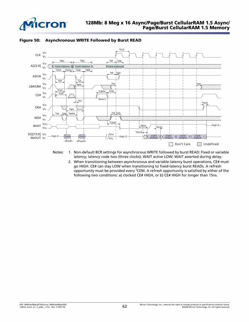
128Mb: 8 Meg x 16 Async/Page/Burst CellularRAM 1.5 Async/Page/Burst CellularRAM 1.5 Memory
Figure 50: Asynchronous WRITE Followed by Burst READ
Notes: 1. Non-default BCR settings for asynchronous WRITE followed by burst READ: Fixed or variable latency; latency code two (three clocks); WAIT active LOW; WAIT asserted during delay.
2. When transitioning between asynchronous and variable-latency burst operations, CE# must go HIGH. CE# can stay LOW when transitioning to fixed-latency burst READs. A refresh opportunity must be provided every tCEM. A refresh opportunity is satisfied by either of the following two conditions: a) clocked CE# HIGH, or b) CE# HIGH for longer than 15ns.
tCLK
tSP tHD
tSP
Valid Address
tOHZ
tKOH
tACLK
High-Z
High-Z
Valid Address Valid Address tAVS tAVH tAW tWR
tVP tVS
A[22:0] VIH
VIL
ADV# VIH
VIL
OE# VIH
VIL
WE# VIH
VIL
WAIT
DQ[15:0] IN/OUT
VOH
VOL
CLK VIH
VIL
VIH
VIL
VOH
VOL
CE# VIH
VIL
LB#/UB# VIH
VIL
tCW
tCVS
tWPH tAS
tAS
tWP
tWC
tDH tDW
Data Data High-Z
tHD tSP
tCEW
tSP tHD
tCSP
tWC tWC
tBW
Valid Output
Valid Output
Valid Output
Valid Output
Don’t Care Undefined
tHD
tBOE
tCBPH
Note 2
PDF: 09005aef80ec6f79/Source: 09005aef80ec6f65 Micron Technology, Inc., reserves the right to change products or specifications without notice.128mb_burst_cr1_5_p26z__2.fm - Rev. H 9/07 EN 62 ©2004 Micron Technology, Inc. All rights reserved.
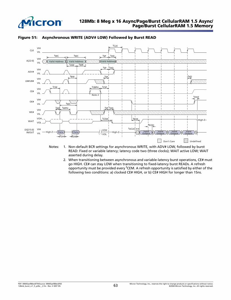
128Mb: 8 Meg x 16 Async/Page/Burst CellularRAM 1.5 Async/Page/Burst CellularRAM 1.5 Memory
Figure 51: Asynchronous WRITE (ADV# LOW) Followed by Burst READ
Notes: 1. Non-default BCR settings for asynchronous WRITE, with ADV# LOW, followed by burst READ: Fixed or variable latency; latency code two (three clocks); WAIT active LOW; WAIT asserted during delay.
2. When transitioning between asynchronous and variable-latency burst operations, CE# must go HIGH. CE# can stay LOW when transitioning to fixed-latency burst READs. A refresh opportunity must be provided every tCEM. A refresh opportunity is satisfied by either of the following two conditions: a) clocked CE# HIGH, or b) CE# HIGH for longer than 15ns.
tCLK
tSP tHD
tHD
Valid Address
tCSP
tKOHtACLK
Valid Output High-Z
Valid Address Valid Address A[22:0] VIH
VIL
ADV# VIH
VIL
OE# VIH
VIL
WE# VIH
VIL
WAIT
DQ[15:0] IN/OUT
VOH
VOL
CLK VIH
VIL
VIH
VIL VOH
VOL
CE# VIH
VIL
LB#/UB# VIH
VIL
tCW
tWPH tWP
tWC
tDH tDW
Data Data High-Z
tHD tSP
tSP tHD
tWC tWC
tBW
tAW tWR tSP
Valid Output
Valid Output
Valid Output
Undefined Don’t Care
tBOE
tOHZ
tCEW
tCBPH
High-Z
Note 2
PDF: 09005aef80ec6f79/Source: 09005aef80ec6f65 Micron Technology, Inc., reserves the right to change products or specifications without notice.128mb_burst_cr1_5_p26z__2.fm - Rev. H 9/07 EN 63 ©2004 Micron Technology, Inc. All rights reserved.
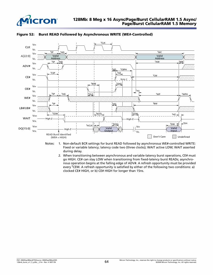
128Mb: 8 Meg x 16 Async/Page/Burst CellularRAM 1.5 Async/Page/Burst CellularRAM 1.5 Memory
Figure 52: Burst READ Followed by Asynchronous WRITE (WE#-Controlled)
Notes: 1. Non-default BCR settings for burst READ followed by asynchronous WE#-controlled WRITE: Fixed or variable latency; latency code two (three clocks); WAIT active LOW; WAIT asserted during delay.
2. When transitioning between asynchronous and variable-latency burst operations, CE# must go HIGH. CE# can stay LOW when transitioning from fixed-latency burst READs; asynchro-nous operation begins at the falling edge of ADV#. A refresh opportunity must be provided every tCEM. A refresh opportunity is satisfied by either of the following two conditions: a) clocked CE# HIGH, or b) CE# HIGH for longer than 15ns.
A[22:0]VIH
VIL
ADV#VIH
VIL
CE#VIH
VIL
OE#VIH
VIL
WE#VIH
VIL
WAIT
DQ[15:0]
VOH
VOL
CLKVIH
VIL
VOH
VOL
VIH
VIL
tSP
tCLK
tACLK
tCEW
tHD
tAW
tCW
tWR
ValidOutput
ValidAddress
High-Z
tKOH tDW
tOHZ
tSP
LB#/UB#VIH
VIL
tCSP
High-Z
tOLZtHD tWP tWPH
tAS
tDH
tHD tBWtSP
tHZ
tHD
tSP
UndefinedDon’t CareREAD Burst Identified
(WE# = HIGH)
tWC
tHD
tKHTL
tBOE
ValidAddress
ValidInput
High-Z
tCEW tHZ
tCBPH
Note 2
PDF: 09005aef80ec6f79/Source: 09005aef80ec6f65 Micron Technology, Inc., reserves the right to change products or specifications without notice.128mb_burst_cr1_5_p26z__2.fm - Rev. H 9/07 EN 64 ©2004 Micron Technology, Inc. All rights reserved.

128Mb: 8 Meg x 16 Async/Page/Burst CellularRAM 1.5 Async/Page/Burst CellularRAM 1.5 Memory
Figure 53: Burst READ Followed by Asynchronous WRITE Using ADV#
Notes: 1. Non-default BCR settings for burst READ followed by asynchronous WRITE using ADV#: Fixed or variable latency; latency code two (three clocks); WAIT active LOW; WAIT asserted during delay.
2. When transitioning between asynchronous and variable-latency burst operations, CE# must go HIGH. CE# can stay LOW when transitioning from fixed-latency burst READs; asynchro-nous operation begins at the falling edge of ADV#. A refresh opportunity must be provided every tCEM. A refresh opportunity is satisfied by either of the following two conditions: a) clocked CE# HIGH, or b) CE# HIGH for longer than 15ns.
A[22:0] VIH
VIL
ADV# VIH
VIL
CE# VIH
VIL
OE# VIH
VIL
WE# VIH
VIL
WAIT
DQ[15:0]
VOH
VOL
CLK VIH
VIL
VOH
VOL
tSP
tCLK
tCEW
tHD
tVS tAVS tAVH
tAW
tCW
Valid Output
Valid Address
High-Z
tKOH tDW
tOHZ
tSP tHD tVP
LB#/UB# VIH
VIL
tCSP
High-Z
tOLZ tHD tWP tWPH tAS
tDH
tHD tBW tSP
tHZ
tSP
Undefined Don’t Care READ Burst Identified
(WE# = HIGH)
tKHTL
Valid Address
Valid Input
High-Z
tCEW tHZ
tCBPH
tACLK
tBOE
tAS tHD
Note 2
VIH
VIL
PDF: 09005aef80ec6f79/Source: 09005aef80ec6f65 Micron Technology, Inc., reserves the right to change products or specifications without notice.128mb_burst_cr1_5_p26z__2.fm - Rev. H 9/07 EN 65 ©2004 Micron Technology, Inc. All rights reserved.
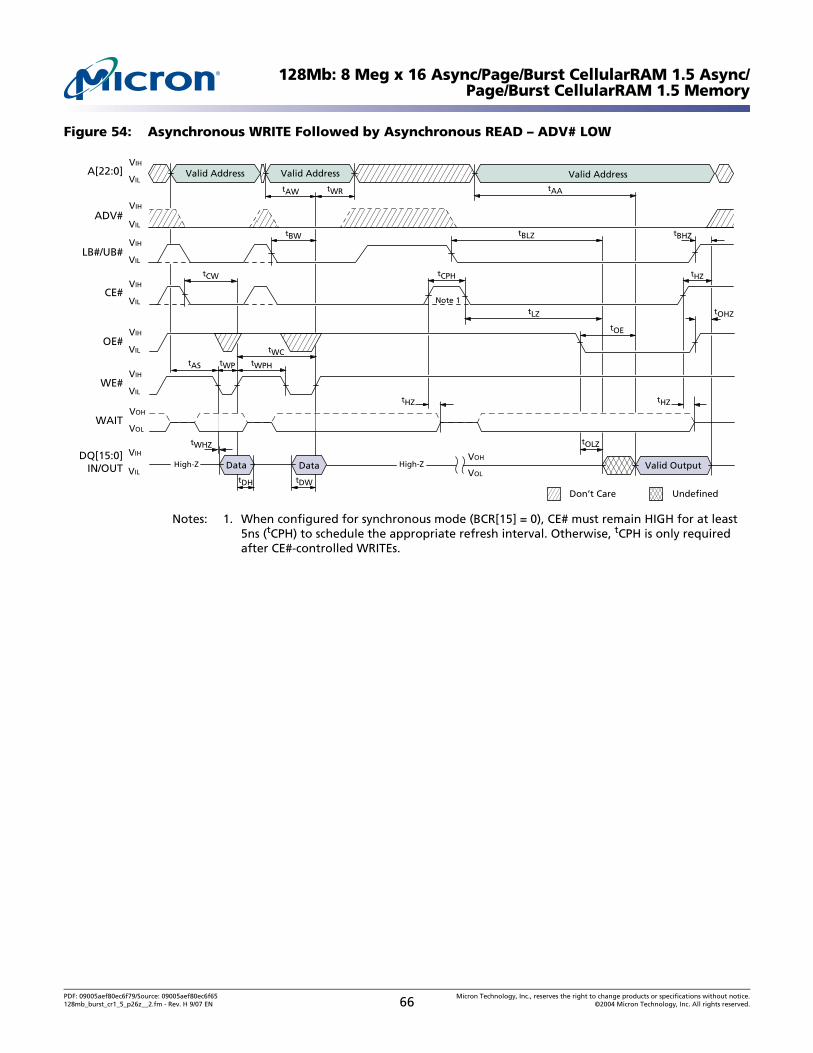
128Mb: 8 Meg x 16 Async/Page/Burst CellularRAM 1.5 Async/Page/Burst CellularRAM 1.5 Memory
Figure 54: Asynchronous WRITE Followed by Asynchronous READ – ADV# LOW
Notes: 1. When configured for synchronous mode (BCR[15] = 0), CE# must remain HIGH for at least 5ns (tCPH) to schedule the appropriate refresh interval. Otherwise, tCPH is only required after CE#-controlled WRITEs.
Valid Address Valid AddressA[22:0]VIH
VIL
ADV#VIH
VIL
OE#
WE#
WAIT
DQ[15:0]IN/OUT
VOH
VOL
VIH
VIL
VOH
VOL
CE#
LB#/UB#VIH
VIL
VIH
VIL
VIH
VIL
VIH
VIL
tCW
tWPHtWPtAS
tWC
tDH tDW
DataHigh-Z
Valid AddresstAA
tBHZ
tCPH
Valid OutputHigh-Z
tOE
tOLZ
tLZ
tBLZ
tOHZ
tHZ
tAW tWR
tBW
tWHZ
tHZ tHZ
Don’t Care Undefined
Data
Note 1
PDF: 09005aef80ec6f79/Source: 09005aef80ec6f65 Micron Technology, Inc., reserves the right to change products or specifications without notice.128mb_burst_cr1_5_p26z__2.fm - Rev. H 9/07 EN 66 ©2004 Micron Technology, Inc. All rights reserved.
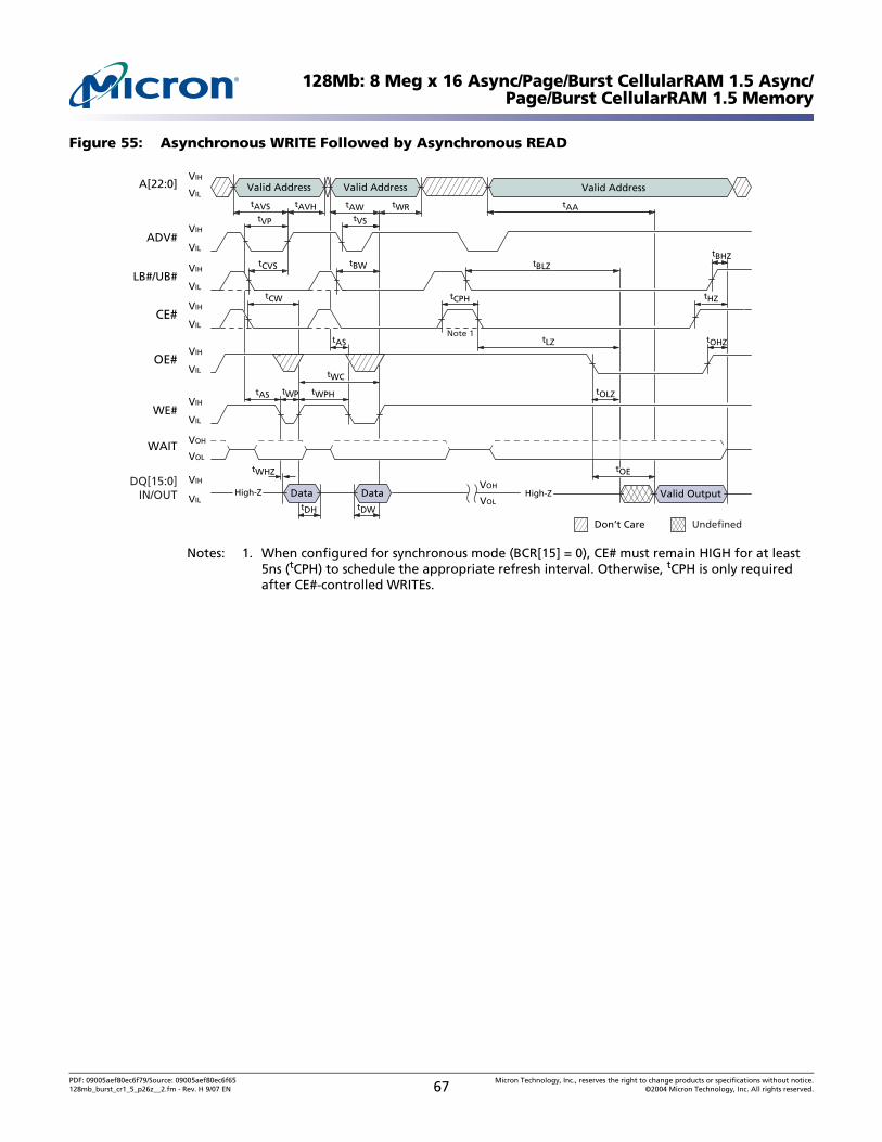
128Mb: 8 Meg x 16 Async/Page/Burst CellularRAM 1.5 Async/Page/Burst CellularRAM 1.5 Memory
Figure 55: Asynchronous WRITE Followed by Asynchronous READ
Notes: 1. When configured for synchronous mode (BCR[15] = 0), CE# must remain HIGH for at least 5ns (tCPH) to schedule the appropriate refresh interval. Otherwise, tCPH is only required after CE#-controlled WRITEs.
Valid Address Valid Address
tAVS tAVHtVP tVS
A[22:0]VIH
VIL
VIH
VIL
VIH
VIL
VIH
VIL
VIH
VIL
VIH
VIL
ADV#
OE#
WE#
WAIT
DQ[15:0]IN/OUT
VOH
VOL
VIH
VIL
VOH
VOL
CE#
LB#/UB#
tCW
tWPHtAS tWP
tWC
tDH tDW
Data DataHigh-Z
Valid Address
tAA
tBHZ
tCPH
Valid OutputHigh-Z
tCVS
tOLZ
tLZtAS
tBLZ
tOHZ
tHZ
tAW tWR
tBW
tWHZ
UndefinedDon’t Care
tOE
Note 1
PDF: 09005aef80ec6f79/Source: 09005aef80ec6f65 Micron Technology, Inc., reserves the right to change products or specifications without notice.128mb_burst_cr1_5_p26z__2.fm - Rev. H 9/07 EN 67 ©2004 Micron Technology, Inc. All rights reserved.
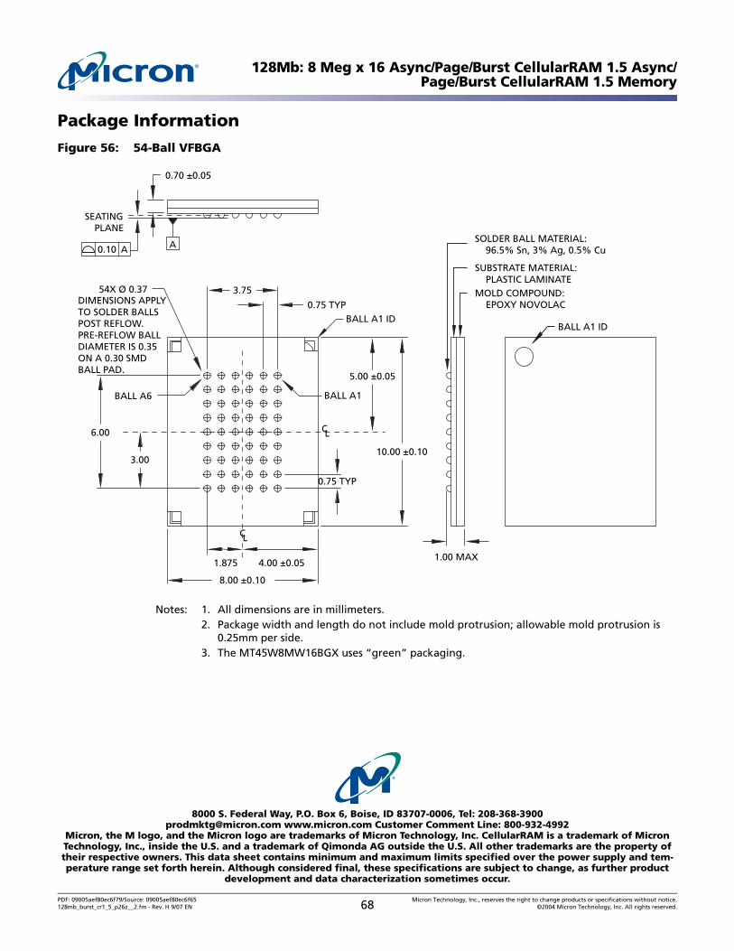
128Mb: 8 Meg x 16 Async/Page/Burst CellularRAM 1.5 Async/Page/Burst CellularRAM 1.5 Memory
Package Information
Figure 56: 54-Ball VFBGA
Notes: 1. All dimensions are in millimeters. 2. Package width and length do not include mold protrusion; allowable mold protrusion is
0.25mm per side.3. The MT45W8MW16BGX uses “green” packaging.
BALL A1 ID
1.00 MAX
MOLD COMPOUND: EPOXY NOVOLAC
SUBSTRATE MATERIAL: PLASTIC LAMINATE
SOLDER BALL MATERIAL: 96.5% Sn, 3% Ag, 0.5% Cu
BALL A6 BALL A1
8.00 ±0.10
4.00 ±0.051.875
BALL A1 ID
54X Ø 0.37DIMENSIONS APPLYTO SOLDER BALLS POST REFLOW.PRE-REFLOW BALLDIAMETER IS 0.35ON A 0.30 SMDBALL PAD.
C L
C L
0.75 TYP
5.00 ±0.05
3.00
6.00
10.00 ±0.10
0.70 ±0.05
0.10 A A
SEATINGPLANE
3.75
0.75 TYP
®
8000 S. Federal Way, P.O. Box 6, Boise, ID 83707-0006, Tel: [email protected] www.micron.com Customer Comment Line: 800-932-4992
Micron, the M logo, and the Micron logo are trademarks of Micron Technology, Inc. CellularRAM is a trademark of Micron Technology, Inc., inside the U.S. and a trademark of Qimonda AG outside the U.S. All other trademarks are the property of their respective owners. This data sheet contains minimum and maximum limits specified over the power supply and tem-perature range set forth herein. Although considered final, these specifications are subject to change, as further product
development and data characterization sometimes occur.
PDF: 09005aef80ec6f79/Source: 09005aef80ec6f65 Micron Technology, Inc., reserves the right to change products or specifications without notice.128mb_burst_cr1_5_p26z__2.fm - Rev. H 9/07 EN 68 ©2004 Micron Technology, Inc. All rights reserved.