Embed Size (px)
Citation preview
HY5DU283222F
128M(4Mx32) GDDR SDRAMHY5DU283222F
This document is a general product description and is subject to change without notice. Hynix Electronics does not assume any respon-sibility for use of circuits described. No patent licenses are implied.Rev. 1.2/Sep. 02 1
Downloaded from Elcodis.com electronic components distributor
Rev. 1.2/Sep. 02 2
HY5DU283222F
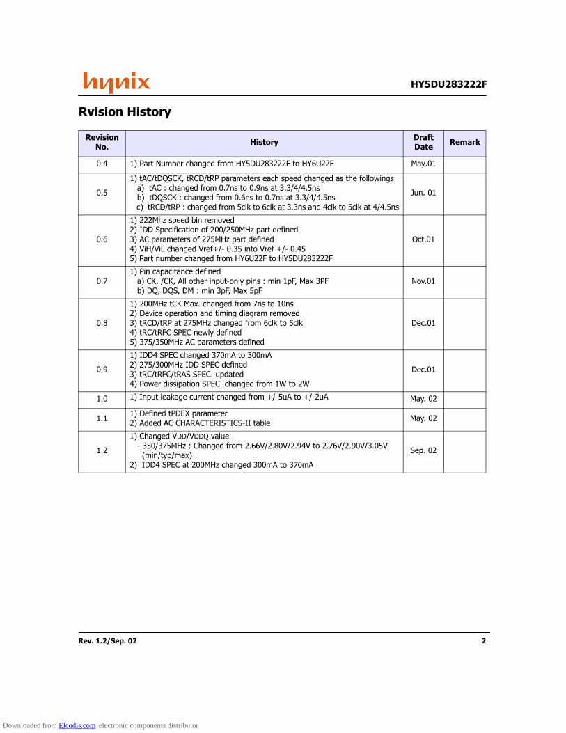
Rvision History
Revision No. History Draft
Date Remark
0.4 1) Part Number changed from HY5DU283222F to HY6U22F May.01
0.5
1) tAC/tDQSCK, tRCD/tRP parameters each speed changed as the followings a) tAC : changed from 0.7ns to 0.9ns at 3.3/4/4.5ns b) tDQSCK : changed from 0.6ns to 0.7ns at 3.3/4/4.5ns c) tRCD/tRP : changed from 5clk to 6clk at 3.3ns and 4clk to 5clk at 4/4.5ns
Jun. 01
0.6
1) 222Mhz speed bin removed2) IDD Specification of 200/250MHz part defined3) AC parameters of 275MHz part defined4) ViH/ViL changed Vref+/- 0.35 into Vref +/- 0.45 5) Part number changed from HY6U22F to HY5DU283222F
Oct.01
0.71) Pin capacitance defined a) CK, /CK, All other input-only pins : min 1pF, Max 3PF b) DQ, DQS, DM : min 3pF, Max 5pF
Nov.01
0.8
1) 200MHz tCK Max. changed from 7ns to 10ns2) Device operation and timing diagram removed3) tRCD/tRP at 275MHz changed from 6clk to 5clk4) tRC/tRFC SPEC newly defined5) 375/350MHz AC parameters defined
Dec.01
0.9
1) IDD4 SPEC changed 370mA to 300mA2) 275/300MHz IDD SPEC defined3) tRC/tRFC/tRAS SPEC. updated4) Power dissipation SPEC. changed from 1W to 2W
Dec.01
1.0 1) Input leakage current changed from +/-5uA to +/-2uA May. 02
1.1 1) Defined tPDEX parameter2) Added AC CHARACTERISTICS-II table May. 02
1.2
1) Changed VDD/VDDQ value - 350/375MHz : Changed from 2.66V/2.80V/2.94V to 2.76V/2.90V/3.05V (min/typ/max) 2) IDD4 SPEC at 200MHz changed 300mA to 370mA
Sep. 02
Downloaded from Elcodis.com electronic components distributor
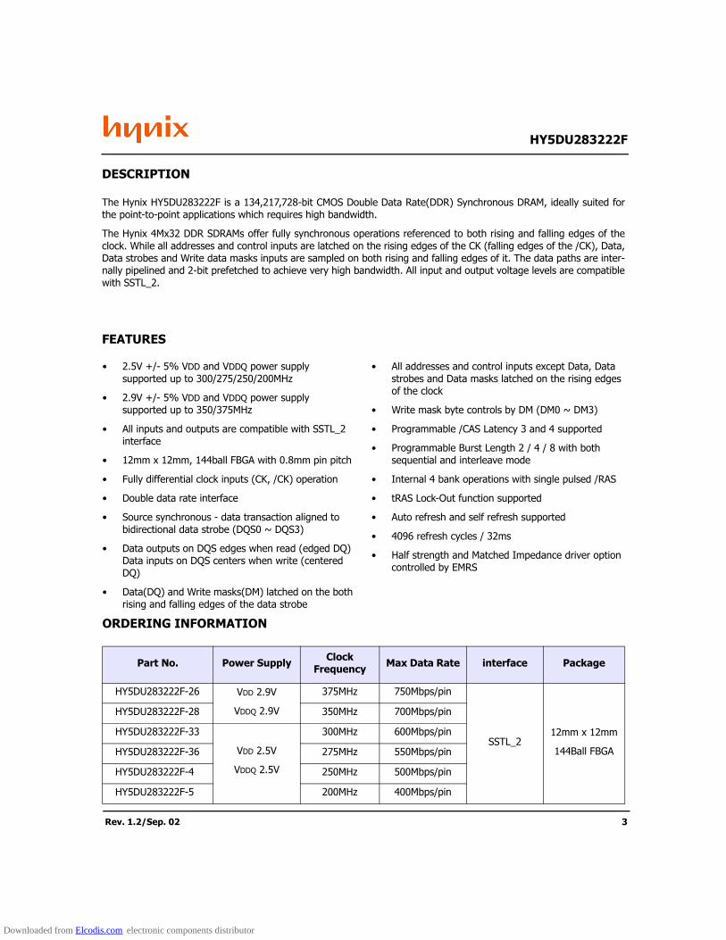
DESCRIPTION
The Hynix HY5DU283222F is a 134,217,728-bit CMOS Double Data Rate(DDR) Synchronous DRAM, ideally suited forthe point-to-point applications which requires high bandwidth.
The Hynix 4Mx32 DDR SDRAMs offer fully synchronous operations referenced to both rising and falling edges of theclock. While all addresses and control inputs are latched on the rising edges of the CK (falling edges of the /CK), Data,Data strobes and Write data masks inputs are sampled on both rising and falling edges of it. The data paths are inter-nally pipelined and 2-bit prefetched to achieve very high bandwidth. All input and output voltage levels are compatiblewith SSTL_2.
FEATURES
• 2.5V +/- 5% VDD and VDDQ power supply supported up to 300/275/250/200MHz
• 2.9V +/- 5% VDD and VDDQ power supply supported up to 350/375MHz
• All inputs and outputs are compatible with SSTL_2 interface
• 12mm x 12mm, 144ball FBGA with 0.8mm pin pitch
• Fully differential clock inputs (CK, /CK) operation
• Double data rate interface
• Source synchronous - data transaction aligned to bidirectional data strobe (DQS0 ~ DQS3)
• Data outputs on DQS edges when read (edged DQ) Data inputs on DQS centers when write (centered DQ)
• Data(DQ) and Write masks(DM) latched on the both rising and falling edges of the data strobe
• All addresses and control inputs except Data, Data strobes and Data masks latched on the rising edges of the clock
• Write mask byte controls by DM (DM0 ~ DM3)
• Programmable /CAS Latency 3 and 4 supported
• Programmable Burst Length 2 / 4 / 8 with both sequential and interleave mode
• Internal 4 bank operations with single pulsed /RAS
• tRAS Lock-Out function supported
• Auto refresh and self refresh supported
• 4096 refresh cycles / 32ms
• Half strength and Matched Impedance driver option controlled by EMRS
ORDERING INFORMATION
Part No. Power Supply Clock Frequency Max Data Rate interface Package
HY5DU283222F-26 VDD 2.9V
VDDQ 2.9V
375MHz 750Mbps/pin
SSTL_212mm x 12mm
144Ball FBGA
HY5DU283222F-28 350MHz 700Mbps/pin
HY5DU283222F-33
VDD 2.5V
VDDQ 2.5V
300MHz 600Mbps/pin
HY5DU283222F-36 275MHz 550Mbps/pin
HY5DU283222F-4 250MHz 500Mbps/pin
HY5DU283222F-5 200MHz 400Mbps/pin
HY5DU283222F
Rev. 1.2/Sep. 02 3
Downloaded from Elcodis.com electronic components distributor
Rev. 1.2/Sep. 02 4
HY5DU283222F
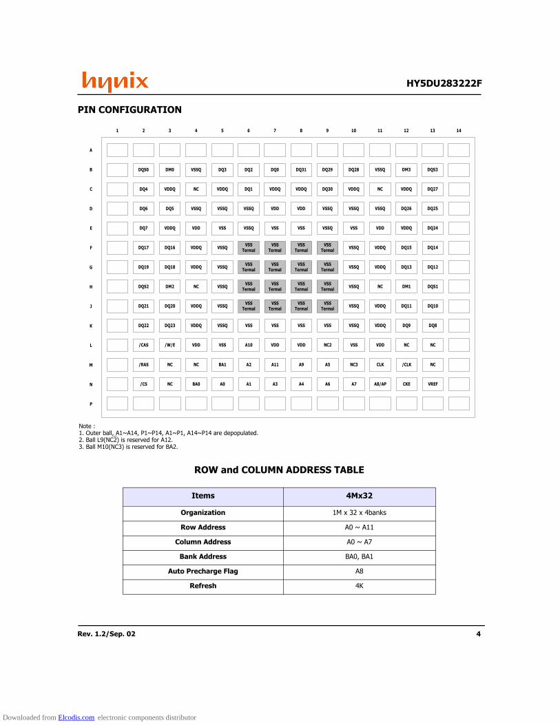
PIN CONFIGURATION
ROW and COLUMN ADDRESS TABLE
Items 4Mx32
Organization 1M x 32 x 4banks
Row Address A0 ~ A11
Column Address A0 ~ A7
Bank Address BA0, BA1
Auto Precharge Flag A8
Refresh 4K
Note :1. Outer ball, A1~A14, P1~P14, A1~P1, A14~P14 are depopulated.2. Ball L9(NC2) is reserved for A12.3. Ball M10(NC3) is reserved for BA2.
A
B
C
D
E
F
G
H
J
K
L
M
N
P
1 2 3 4 5 6 7 8 9 10 11 12 13 14
DQS0 DM0 VSSQ DQ3 DQ2 DQ0 DQ31 DQ29 DQ28 VSSQ DM3 DQS3
DQ4 VDDQ NC VDDQ DQ1 VDDQ VDDQ DQ30 VDDQ NC VDDQ DQ27
DQ6 DQ5 VSSQ VSSQ VSSQ VDD VDD VSSQ VSSQ VSSQ DQ26 DQ25
DQ7 VDDQ VDD VSS VSSQ VSS VSS VSSQ VSS VDD VDDQ DQ24
DQ17 DQ16 VDDQ VSSQ VSSTermal
VSSTermal
VSSTermal
VSSTermal VSSQ VDDQ DQ15 DQ14
DQ19 DQ18 VDDQ VSSQ VSSTermal
VSSTermal
VSSTermal
VSSTermal VSSQ VDDQ DQ13 DQ12
DQS2 DM2 NC VSSQ VSSTermal
VSSTermal
VSSTermal
VSSTermal VSSQ NC DM1 DQS1
DQ21 DQ20 VDDQ VSSQ VSSTermal
VSSTermal
VSSTermal
VSSTermal VSSQ VDDQ DQ11 DQ10
DQ22 DQ23 VDDQ VSSQ VSS VSS VSS VSS VSSQ VDDQ DQ9 DQ8
/CAS /W/E VDD VSS A10 VDD VDD NC2 VSS VDD NC NC
/RAS NC NC BA1 A2 A11 A9 A5 NC3 CLK /CLK NC
/CS NC BA0 A0 A1 A3 A4 A6 A7 A8/AP CKE VREF
Downloaded from Elcodis.com electronic components distributor
Rev. 1.2/Sep. 02 5
HY5DU283222F
PIN DESCRIPTION
PIN TYPE DESCRIPTION
CK, /CK InputClock: CK and /CK are differential clock inputs. All address and control input signals are sampled on the crossing of the positive edge of CK and negative edge of /CK. Output (read) data is referenced to the crossings of CK and /CK (both directions of crossing).
CKE Input
Clock Enable: CKE HIGH activates, and CKE LOW deactivates internal clock signals, and device input buffers and output drivers. Taking CKE LOW provides PRECHARGE POWER DOWN and SELF REFRESH operation (all banks idle), or ACTIVE POWER DOWN (row ACTIVE in any bank). CKE is synchronous for POWER DOWN entry and exit, and for SELF REFRESH entry. CKE is asynchronous for SELF REFRESH exit, and for output disable. CKE must be maintained high throughout READ and WRITE accesses. Input buffers, excluding CK, /CK and CKE are disabled during POWER DOWN. Input buffers, excluding CKE are disabled during SELF REFRESH. CKE is an SSTL_2 input, but will detect an LVCMOS LOW level after Vdd is applied.
/CS InputChip Select : Enables or disables all inputs except CK, /CK, CKE, DQS and DM. All com-mands are masked when CS is registered high. CS provides for external bank selection on systems with multiple banks. CS is considered part of the command code.
BA0, BA1 InputBank Address Inputs: BA0 and BA1 define to which bank an ACTIVE, Read, Write or PRE-CHARGE command is being applied.
A0 ~ A11 Input
Address Inputs: Provide the row address for ACTIVE commands, and the column address and AUTO PRECHARGE bit for READ/WRITE commands, to select one location out of the memory array in the respective bank. A8 is sampled during a precharge command to determine whether the PRECHARGE applies to one bank (A8 LOW) or all banks (A8 HIGH). If only one bank is to be precharged, the bank is selected by BA0, BA1. The address inputs also provide the op code during a MODE REGISTER SET command. BA0 and BA1 define which mode register is loaded during the MODE REGISTER SET command (MRS or EMRS).
/RAS, /CAS, /WE InputCommand Inputs: /RAS, /CAS and /WE (along with /CS) define the command being entered.
DM0 ~ DM3 Input
Input Data Mask: DM(0~3) is an input mask signal for write data. Input data is masked when DM is sampled HIGH along with that input data during a WRITE access. DM is sam-pled on both edges of DQS. Although DM pins are input only, the DM loading matches the DQ and DQS loading. DM0 corresponds to the data on DQ0-Q7; DM1 corresponds to the data on DQ8-Q15; DM2 corresponds to the data on DQ16-Q23; DM3 corresponds to the data on DQ24-Q31.
DQS0 ~ DQS3 I/O
Data Strobe: Output with read data, input with write data. Edge aligned with read data, centered in write data. Used to capture write data. DQS0 corresponds to the data on DQ0-Q7; DQS1 corresponds to the data on DQ8-Q15; DQS2 corresponds to the data on DQ16-Q23; DQS3 corresponds to the data on DQ24-Q31
DQ0 ~ DQ31 I/O Data input / output pin : Data Bus
VDD/VSS Supply Power supply for internal circuits and input buffers.
VDDQ/VSSQ Supply Power supply for output buffers for noise immunity.
VREF Supply Reference voltage for inputs for SSTL interface.
NC NC No connection.
Downloaded from Elcodis.com electronic components distributor
Rev. 1.2/Sep. 02 6
HY5DU283222F
FUNCTIONAL BLOCK DIAGRAM
4Banks x 1Mbit x 32 I/O Double Data Rate Synchronous DRAM
CommandDecoder
CLK/CLKCKE/CS/RAS/CAS/WE
DM(0~3)
AddressBuffer
A0-11
BankControl 1Mx32/Bank0
Column Decoder
Column Address Counter
Sense AMP
2-bit PrefetchU
nit
1Mx32 /Bank1
1Mx32 /Bank2
1Mx32 /Bank3
ModeRegister
RowDecoder
Input BufferO
utput Buffer
Data StrobeTransmitter
Data StrobeReceiver
DQS(0~3)
DS
Write Data Register2-bit Prefetch Unit DS
DQ[0:31]
64 32
32
64
BA0,BA1
DLLBlock
CLK_DLL
CLK, /CLK
ModeRegister
Downloaded from Elcodis.com electronic components distributor
Rev. 1.2/Sep. 02 7
HY5DU283222F
SIMPLIFIED COMMAND TRUTH TABLE
Command CKEn-1 CKEn CS RAS CAS WE ADDRA8/AP BA Note
Extended Mode Register Set H X L L L L OP code 1,2
Mode Register Set H X L L L L OP code 1,2
Device DeselectH X
H X X XX 1
No Operation L H H H
Bank Active H X L L H H RA V 1
ReadH X L H L H CA
LV
1
Read with Autoprecharge H 1,3
WriteH X L H L L CA
LV
1
Write with Autoprecharge H 1,4
Precharge All BanksH X L L H L X
H X 1,5
Precharge selected Bank L V 1
Read Burst Stop H X L H H L X 1
Auto Refresh H H L L L H X 1
Self Refresh
Entry H L L L L H
X
1
Exit L HH X X X
1L H H H
Precharge Power Down Mode
Entry H LH X X X
X
1
L H H H 1
Exit L HH X X X 1
L H H H 1
Active Power Down Mode
Entry H LH X X X
X
1
L V V V 1
Exit L H X 1
Note : 1. DM(0~3) states are Don’t Care. Refer to below Write Mask Truth Table.2. OP Code(Operand Code) consists of A0~A11 and BA0~BA1 used for Mode Register setting during Extended MRS or MRS. Before entering Mode Register Set mode, all banks must be in a precharge state and MRS command can be issued after tRP period from Prechagre command.3. If a Read with Autoprecharge command is detected by memory component in CK(n), then there will be no command presented to activated bank until CK(n+BL/2+tRP).4. If a Write with Autoprecharge command is detected by memory component in CK(n), then there will be no command presented to activated bank until CK(n+BL/2+1+tDPL+tRP). Last Data-In to Prechage delay(tDPL) which is also called Write Recovery Time (tWR) is needed to guarantee that the last data has been completely written.5. If A8/AP is High when Precharge command being issued, BA0/BA1 are ignored and all banks are selected to be precharged.
( H=Logic High Level, L=Logic Low Level, X=Don’t Care, V=Valid Data Input, OP Code=Operand Code, NOP=No Operation )
Downloaded from Elcodis.com electronic components distributor
Rev. 1.2/Sep. 02 8
HY5DU283222F
WRITE MASK TRUTH TABLE
Function CKEn-1 CKEn /CS, /RAS, /CAS, /WE DM(0~3) ADDR
A8/AP BA Note
Data Write H X X L X 1,2
Data-In Mask H X X H X 1,2
Note : 1. Write Mask command masks burst write data with reference to DQS(0~3) and it is not related with read data.2. DM0 corresponds to the data on DQ0-Q7; DM1 corresponds to the data on DQ8-Q15; DM2 corresponds to the data on DQ16-Q23; DM3 corresponds to the data on DQ24-Q31.
Downloaded from Elcodis.com electronic components distributor
Rev. 1.2/Sep. 02 9
HY5DU283222F
OPERATION COMMAND TRUTH TABLE - I
Current State /CS /RAS /CAS /WE Address Command Action
IDLE
H X X X X DSEL NOP or power down3
L H H H X NOP NOP or power down3
L H H L X BST ILLEGAL4
L H L H BA, CA, AP READ/READAP ILLEGAL4
L H L L BA, CA, AP WRITE/WRITEAP ILLEGAL4
L L H H BA, RA ACT Row Activation
L L H L BA, AP PRE/PALL NOP
L L L H X AREF/SREF Auto Refresh or Self Refresh5
L L L L OPCODE MRS Mode Register Set
ROW
ACTIVE
H X X X X DSEL NOP
L H H H X NOP NOP
L H H L X BST ILLEGAL4
L H L H BA, CA, AP READ/READAP Begin read : optional AP6
L H L L BA, CA, AP WRITE/WRITEAP Begin write : optional AP6
L L H H BA, RA ACT ILLEGAL4
L L H L BA, AP PRE/PALL Precharge7
L L L H X AREF/SREF ILLEGAL11
L L L L OPCODE MRS ILLEGAL11
READ
H X X X X DSEL Continue burst to end
L H H H X NOP Continue burst to end
L H H L X BST Terminate burst
L H L H BA, CA, AP READ/READAP Term burst, new read:optional AP8
L H L L BA, CA, AP WRITE/WRITEAP ILLEGAL
L L H H BA, RA ACT ILLEGAL4
L L H L BA, AP PRE/PALL Term burst, precharge
L L L H X AREF/SREF ILLEGAL11
L L L L OPCODE MRS ILLEGAL11
WRITE
H X X X X DSEL Continue burst to end
L H H H X NOP Continue burst to end
L H H L X BST ILLEGAL4
L H L H BA, CA, AP READ/READAP Term burst, new read:optional AP8
L H L L BA, CA, AP WRITE/WRITEAP Term burst, new write:optional AP
Downloaded from Elcodis.com electronic components distributor
Rev. 1.2/Sep. 02 10
HY5DU283222F
OPERATION COMMAND TRUTH TABLE - II
Current State /CS /RAS /CAS /WE Address Command Action
WRITE
L L H H BA, RA ACT ILLEGAL4
L L H L BA, AP PRE/PALL Term burst, precharge
L L L H X AREF/SREF ILLEGAL11
L L L L OPCODE MRS ILLEGAL11
READWITH
AUTOPRE-CHARGE
H X X X X DSEL Continue burst to end
L H H H X NOP Continue burst to end
L H H L X BST ILLEGAL
L H L H BA, CA, AP READ/READAP ILLEGAL10
L H L L BA, CA, AP WRITE/WRITEAP ILLEGAL10
L L H H BA, RA ACT ILLEGAL4,10
L L H L BA, AP PRE/PALL ILLEGAL4,10
L L L H X AREF/SREF ILLEGAL11
L L L L OPCODE MRS ILLEGAL11
WRITEAUTOPRE-CHARGE
H X X X X DSEL Continue burst to end
L H H H X NOP Continue burst to end
L H H L X BST ILLEGAL
L H L H BA, CA, AP READ/READAP ILLEGAL10
L H L L BA, CA, AP WRITE/WRITEAP ILLEGAL10
L L H H BA, RA ACT ILLEGAL4,10
L L H L BA, AP PRE/PALL ILLEGAL4,10
L L L H X AREF/SREF ILLEGAL11
L L L L OPCODE MRS ILLEGAL11
PRE-CHARGE
H X X X X DSEL NOP-Enter IDLE after tRP
L H H H X NOP NOP-Enter IDLE after tRP
L H H L X BST ILLEGAL4
L H L H BA, CA, AP READ/READAP ILLEGAL4,10
L H L L BA, CA, AP WRITE/WRITEAP ILLEGAL4,10
L L H H BA, RA ACT ILLEGAL4,10
L L H L BA, AP PRE/PALL NOP-Enter IDLE after tRP
L L L H X AREF/SREF ILLEGAL11
L L L L OPCODE MRS ILLEGAL11
Downloaded from Elcodis.com electronic components distributor
Rev. 1.2/Sep. 02 11
HY5DU283222F
OPERATION COMMAND TRUTH TABLE - III
Current State /CS /RAS /CAS /WE Address Command Action
ROWACTIVATING
H X X X X DSEL NOP - Enter ROW ACT after tRCD
L H H H X NOP NOP - Enter ROW ACT after tRCD
L H H L X BST ILLEGAL4
L H L H BA, CA, AP READ/READAP ILLEGAL4,10
L H L L BA, CA, AP WRITE/WRITEAP ILLEGAL4,10
L L H H BA, RA ACT ILLEGAL4,9,10
L L H L BA, AP PRE/PALL ILLEGAL4,10
L L L H X AREF/SREF ILLEGAL11
L L L L OPCODE MRS ILLEGAL11
WRITERECOVERING
H X X X X DSEL NOP - Enter ROW ACT after tWR
L H H H X NOP NOP - Enter ROW ACT after tWR
L H H L X BST ILLEGAL4
L H L H BA, CA, AP READ/READAP ILLEGAL
L H L L BA, CA, AP WRITE/WRITEAP ILLEGAL
L L H H BA, RA ACT ILLEGAL4,10
L L H L BA, AP PRE/PALL ILLEGAL4,11
L L L H X AREF/SREF ILLEGAL11
L L L L OPCODE MRS ILLEGAL11
WRITERECOVERING
WITHAUTOPRE-CHARGE
H X X X X DSEL NOP - Enter precharge after tDPL
L H H H X NOP NOP - Enter precharge after tDPL
L H H L X BST ILLEGAL4
L H L H BA, CA, AP READ/READAP ILLEGAL4,8,10
L H L L BA, CA, AP WRITE/WRITEAP ILLEGAL4,10
L L H H BA, RA ACT ILLEGAL4,10
L L H L BA, AP PRE/PALL ILLEGAL4,11
L L L H X AREF/SREF ILLEGAL11
L L L L OPCODE MRS ILLEGAL11
REFRESHING
H X X X X DSEL NOP - Enter IDLE after tRC
L H H H X NOP NOP - Enter IDLE after tRC
L H H L X BST ILLEGAL11
L H L H BA, CA, AP READ/READAP ILLEGAL11
Downloaded from Elcodis.com electronic components distributor
Rev. 1.2/Sep. 02 12
HY5DU283222F
OPERATION COMMAND TRUTH TABLE - IV
Note : 1. H - Logic High Level, L - Logic Low Level, X - Don’t Care, V - Valid Data Input, BA - Bank Address, AP - AutoPrecharge Address, CA - Column Address, RA - Row Address, NOP - NO Operation. 2. All entries assume that CKE was active(high level) during the preceding clock cycle.3. If both banks are idle and CKE is inactive(low level), then in power down mode.4. Illegal to bank in specified state. Function may be legal in the bank indicated by Bank Address(BA) depending on the state of that bank.5. If both banks are idle and CKE is inactive(low level), then self refresh mode.6. Illegal if tRCD is not met. 7. Illegal if tRAS is not met. 8. Must satisfy bus contention, bus turn around, and/or write recovery requirements.9. Illegal if tRRD is not met. 10. Illegal for single bank, but legal for other banks in multi-bank devices.11. Illegal for all banks.
Current State /CS /RAS /CAS /WE Address Command Action
WRITE
L H L L BA, CA, AP WRITE/WRITEAP ILLEGAL11
L L H H BA, RA ACT ILLEGAL11
L L H L BA, AP PRE/PALL ILLEGAL11
L L L H X AREF/SREF ILLEGAL11
L L L L OPCODE MRS ILLEGAL11
MODEREGISTER
ACCESSING
H X X X X DSEL NOP - Enter IDLE after tMRD
L H H H X NOP NOP - Enter IDLE after tMRD
L H H L X BST ILLEGAL11
L H L H BA, CA, AP READ/READAP ILLEGAL11
L H L L BA, CA, AP WRITE/WRITEAP ILLEGAL11
L L H H BA, RA ACT ILLEGAL11
L L H L BA, AP PRE/PALL ILLEGAL11
L L L H X AREF/SREF ILLEGAL11
L L L L OPCODE MRS ILLEGAL11
Downloaded from Elcodis.com electronic components distributor
Rev. 1.2/Sep. 02 13
HY5DU283222F
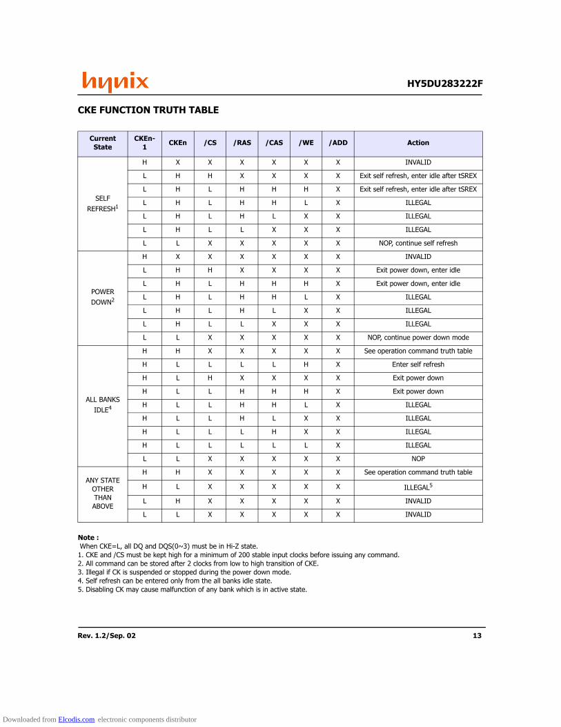
CKE FUNCTION TRUTH TABLE
Note : When CKE=L, all DQ and DQS(0~3) must be in Hi-Z state. 1. CKE and /CS must be kept high for a minimum of 200 stable input clocks before issuing any command.2. All command can be stored after 2 clocks from low to high transition of CKE.3. Illegal if CK is suspended or stopped during the power down mode.4. Self refresh can be entered only from the all banks idle state.5. Disabling CK may cause malfunction of any bank which is in active state.
Current State
CKEn-1 CKEn /CS /RAS /CAS /WE /ADD Action
SELFREFRESH1
H X X X X X X INVALID
L H H X X X X Exit self refresh, enter idle after tSREX
L H L H H H X Exit self refresh, enter idle after tSREX
L H L H H L X ILLEGAL
L H L H L X X ILLEGAL
L H L L X X X ILLEGAL
L L X X X X X NOP, continue self refresh
POWER DOWN2
H X X X X X X INVALID
L H H X X X X Exit power down, enter idle
L H L H H H X Exit power down, enter idle
L H L H H L X ILLEGAL
L H L H L X X ILLEGAL
L H L L X X X ILLEGAL
L L X X X X X NOP, continue power down mode
ALL BANKS IDLE4
H H X X X X X See operation command truth table
H L L L L H X Enter self refresh
H L H X X X X Exit power down
H L L H H H X Exit power down
H L L H H L X ILLEGAL
H L L H L X X ILLEGAL
H L L L H X X ILLEGAL
H L L L L L X ILLEGAL
L L X X X X X NOP
ANY STATE OTHERTHAN ABOVE
H H X X X X X See operation command truth table
H L X X X X X ILLEGAL5
L H X X X X X INVALID
L L X X X X X INVALID
Downloaded from Elcodis.com electronic components distributor
Rev. 1.2/Sep. 02 14
HY5DU283222F
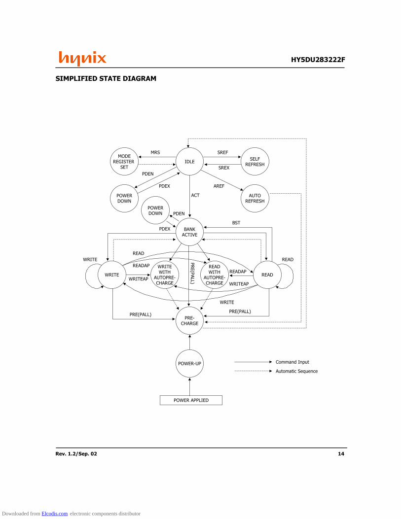
SIMPLIFIED STATE DIAGRAM
MRS SREF
SREXPDEN
PDEX
ACT
AREF
PDEX
PDEN
BST
READWRITE
WRITE
WRITEAPWRITEAP
READ
READAPREADAP
PRE(PALL)PRE(PALL)
PRE(PALL)
Command Input
Automatic Sequence
IDLE
AUTOREFRESH
PRE-CHARGE
POWER-UP
POWER APPLIED
MODEREGISTER
SET
POWERDOWN
WRITEWITH
AUTOPRE-CHARGE
POWERDOWN
WRITE
READWITH
AUTOPRE-CHARGE
BANKACTIVE
READ
SELFREFRESH
Downloaded from Elcodis.com electronic components distributor
Rev. 1.2/Sep. 02 15
HY5DU283222F
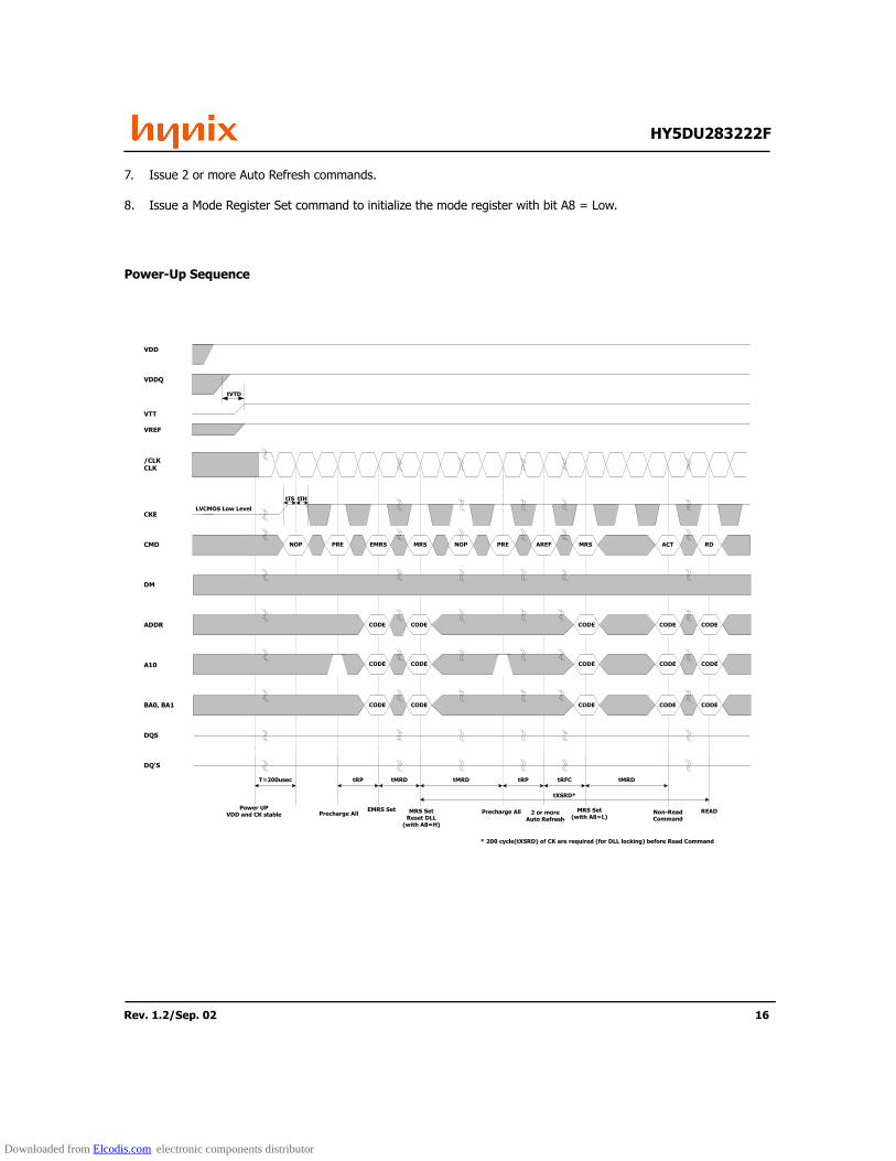
POWER-UP SEQUENCE AND DEVICE INITIALIZATION
DDR SDRAMs must be powered up and initialized in a predefined manner. Operational procedures other than thosespecified may result in undefined operation. Power must first be applied to VDD, then to VDDQ, and finally to VREF (andto the system VTT). VTT must be applied after VDDQ to avoid device latch-up, which may cause permanent damage tothe device. VREF can be applied anytime after VDDQ, but is expected to be nominally coincident with VTT. Except forCKE, inputs are not recognized as valid until after VREF is applied. CKE is an SSTL_2 input, but will detect an LVCMOSLOW level after VDD is applied. Maintaining an LVCMOS LOW level on CKE during power-up is required to guaranteethat the DQ and DQS outputs will be in the High-Z state, where they will remain until driven in normal operation (by aread access). After all power supply and reference voltages are stable, and the clock is stable, the DDR SDRAMrequires a 200us delay prior to applying an executable command.
Once the 200us delay has been satisfied, a DESELECT or NOP command should be applied, and CKE should bebrought HIGH. Following the NOP command, a PRECHARGE ALL command should be applied. Next a EXTENDEDMODE REGISTER SET command should be issued for the Extended Mode Register, to enable the DLL, then a MODEREGISTER SET command should be issued for the Mode Register, to reset the DLL, and to program the operatingparameters. After the DLL reset, tXSRD(DLL locking time) should be satisfied for read command. After the Mode Reg-ister set command, a PRECHARGE ALL command should be applied, placing the device in the all banks idle state.
Once in the idle state, two AUTO REFRESH cycles must be performed. Additionally, a MODE REGISTER SET commandfor the Mode Register, with the reset DLL bit deactivated low (i.e. to program operating parameters without resettingthe DLL) must be performed. Following these cycles, the DDR SDRAM is ready for normal operation.
1. Apply power - VDD, VDDQ, VTT, VREF in the following power up sequencing and attempt to maintain CKE at LVC-MOS low state. (All the other input pins may be undefined.)
• VDD and VDDQ are driven from a single power converter output.
• VTT is limited to 1.44V (reflecting VDDQ(max)/2 + 50mV VREF variation + 40mV VTT variation.
• VREF tracks VDDQ/2.
• A minimum resistance of 42 Ohms (22 ohm series resistor + 22 ohm parallel resistor - 5% tolerance) limits the input current from the VTT supply into any pin.
• If the above criteria cannot be met by the system design, then the following sequencing and voltage relation-ship must be adhered to during power up.
2. Start clock and maintain stable clock for a minimum of 200usec.
3. After stable power and clock, apply NOP condition and take CKE high.
4. Issue Extended Mode Register Set (EMRS) to enable DLL.
5. Issue Mode Register Set (MRS) to reset DLL and set device to idle state with bit A8=High. (An additional 200 cycles(tXSRD) of clock are required for locking DLL)
6. Issue Precharge commands for all banks of the device.
Votage description Sequencing Voltage relationship to avoid latch-up
VDDQ After or with VDD < VDD + 0.3V
VTT After or with VDDQ < VDDQ + 0.3V
VREF After or with VDDQ < VDDQ + 0.3V
Downloaded from Elcodis.com electronic components distributor
Rev. 1.2/Sep. 02 16
HY5DU283222F
7. Issue 2 or more Auto Refresh commands.
8. Issue a Mode Register Set command to initialize the mode register with bit A8 = Low.
Power-Up Sequence
CODECODE CODE CODECODE
CODECODE CODE CODECODE
CODE CODECODECODECODE
NOP PRE MRSEMRS PRENOP MRSAREF ACT RD
VDD
VDDQ
VTT
VREF
/CLKCLK
CKE
CMD
DM
ADDR
A10
BA0, BA1
DQS
DQ'S
LVCMOS Low Level
tIS tIH
tVTD
T=200usec tRP tMRD tRP tRFC tMRD
tXSRD*
READNon-ReadCommand
Power UPVDD and CK stable Precharge All
EMRS Set MRS SetReset DLL
(with A8=H)
Precharge All 2 or moreAuto Refresh
MRS Set(with A8=L)
* 200 cycle(tXSRD) of CK are required (for DLL locking) before Read Command
tMRD
Downloaded from Elcodis.com electronic components distributor
Rev. 1.2/Sep. 02 17
HY5DU283222F
MODE REGISTER SET (MRS)
The mode register is used to store the various operating modes such as /CAS latency, addressing mode, burst length,burst type, test mode, DLL reset. The mode register is program via MRS command. This command is issued by the lowsignals of /RAS, /CAS, /CS, /WE and BA0. This command can be issued only when all banks are in idle state and CKEmust be high at least one cycle before the Mode Register Set Command can be issued. Two cycles are required to writethe data in mode register. During the the MRS cycle, any command cannot be issued. Once mode register field isdetermined, the information will be held until resetted by another MRS command.
BA1 BA0 A11 A10 A9 A8 A7 A6 A5 A4 A3 A2 A1 A0
0 0 RFU DR TM CAS Latency BT Burst Length
A2 A1 A0Burst Length
Sequential Interleave
0 0 0 Reserved Reserved
0 0 1 2 2
0 1 0 4 4
0 1 1 8 8
1 0 0 Reserved Reserved
1 0 1 Reserved Reserved
1 1 0 Reserved Reserved
1 1 1 Reserved Reserved
A3 Burst Type
0 Sequential
1 Interleave
A6 A5 A4 CAS Latency
0 0 0 Reserved
0 0 1 Reserved
0 1 0 Reserved
0 1 1 3
1 0 0 4
1 0 1 Reserved
1 1 0 Reserved
1 1 1 Reserved
A7 Test Mode
0 Normal
1Vendor
test mode
A8 DLL Reset
0 No
1 Yes
BA0 MRS Type
0 MRS
1 EMRS
Downloaded from Elcodis.com electronic components distributor
Rev. 1.2/Sep. 02 18
HY5DU283222F
BURST DEFINITION
BURST LENGTH & TYPE
Read and write accesses to the DDR SDRAM are burst oriented, with the burst length being programmable. The burstlength determines the maximum number of column locations that can be accessed for a given Read or Write com-mand. Burst lengths of 2, 4 or 8 locations are available for both the sequential and the interleaved burst types.Reserved states should not be used, as unknown operation or incompatibility with future versions may result.
When a Read or Write command is issued, a block of columns equal to the burst length is effectively selected. Allaccesses for that burst take place within this block, meaning that the burst wraps within the block if a boundary isreached. The block is uniquely selected by A1-Ai when the burst length is set to two, by A2-Ai when the burst length isset to four and by A3-Ai when the burst length is set to eight (where Ai is the most significant column address bit for agiven configuration). The remaining (least significant) address bit(s) is (are) used to select the starting location withinthe block. The programmed burst length applies to both Read and Write bursts.
Accesses within a given burst may be programmed to be either sequential or interleaved; this is referred to as theburst type and is selected via bit A3. The ordering of accesses within a burst is determined by the burst length, theburst type and the starting column address, as shown in Burst Definitionon Table
Burst Length Starting Address (A2,A1,A0) Sequential Interleave
2XX0 0, 1 0, 1
XX1 1, 0 1, 0
4
X00 0, 1, 2, 3 0, 1, 2, 3
X01 1, 2, 3, 0 1, 0, 3, 2
X10 2, 3, 0, 1 2, 3, 0, 1
X11 3, 0, 1, 2 3, 2, 1, 0
8
000 0, 1, 2, 3, 4, 5, 6, 7 0, 1, 2, 3, 4, 5, 6, 7
001 1, 2, 3, 4, 5, 6, 7, 0 1, 0, 3, 2, 5, 4, 7, 6
010 2, 3, 4, 5, 6, 7, 0, 1 2, 3, 0, 1, 6, 7, 4, 5
011 3, 4, 5, 6, 7, 0, 1, 2 3, 2, 1, 0, 7, 6, 5, 4
100 4, 5, 6, 7, 0, 1, 2, 3 4, 5, 6, 7, 0, 1, 2, 3
101 5, 6, 7, 0, 1, 2, 3, 4 5, 4, 7, 6, 1, 0, 3, 2
110 6, 7, 0, 1, 2, 3, 4, 5 6, 7, 4, 5, 2, 3, 0, 1
111 0, 1, 2, 3, 4, 5, 6, 7 7, 6, 5, 4, 3, 2, 1, 0
Downloaded from Elcodis.com electronic components distributor
Rev. 1.2/Sep. 02 19
HY5DU283222F
CAS LATENCY
The Read latency or CAS latency is the delay in clock cycles between the registration of a Read command and theavailability of the first burst of output data. The latency can be programmed 3 or 4 clocks.
If a Read command is registered at clock edge n, and the latency is m clocks, the data is available nominally coincidentwith clock edge n + m.
Reserved states should not be used as unknown operation or incompatibility with future versions may result.
DLL RESET
The DLL must be enabled for normal operation. DLL enable is required during power up initialization, and upon return-ing to normal operation after having disabled the DLL for the purpose of debug or evaluation. The DLL is automaticallydisabled when entering self refresh operation and is automatically re-enabled upon exit of self refresh operation. Anytime the DLL is enabled, 200 clock cycles must occur to allow time for the internal clock to lock to the externallyapplied clock before an any command can be issued.
OUTPUT DRIVER IMPEDANCE CONTROL
This device supports both Half strength driver and Matched impedance driver, intended for lighter load and/or point-to-point environments. Half strength driver is to define about 50% of Full drive strength which is specified to be SSTL_2,Class II, and Matched impedance driver, about 30% of Full drive strength.
Downloaded from Elcodis.com electronic components distributor
Rev. 1.2/Sep. 02 20
HY5DU283222F
EXTENDED MODE REGISTER SET (EMRS)
The Extended Mode Register controls functions beyond those controlled by the Mode Register; these additional func-tions include DLL enable/disable, output driver strength selection(optional). These functions are controlled via the bits shown below. The Extended Mode Register is programmed via the Mode Register Set command ( BA0=1 and BA1=0) and will retain the stored information until it is programmed again or the device loses power.
The Extended Mode Register must be loaded when all banks are idle and no bursts are in progress, and the controller must wait the specified time before initiating any subsequent operation. Violating either of these requirements will result in unspecified operation.
BA1 BA0 A11 A10 A9 A8 A7 A6 A5 A4 A3 A2 A1 A0
0 1 RFU* DS RFU* DS DLL
A0 DLL enable
0 Enable
1 Diable
BA0 MRS Type
0 MRS
1 EMRS
A6 A1 Output Driver Impedance Control
0 0 RFU*
0 1 Half
1 0 RFU*
1 1 Matched Impedance (Weak)
* All bits in RFU address fields must be programmed to Zero, all other states are reserved for future usage.
Downloaded from Elcodis.com electronic components distributor
Rev. 1.2/Sep. 02 21
HY5DU283222F
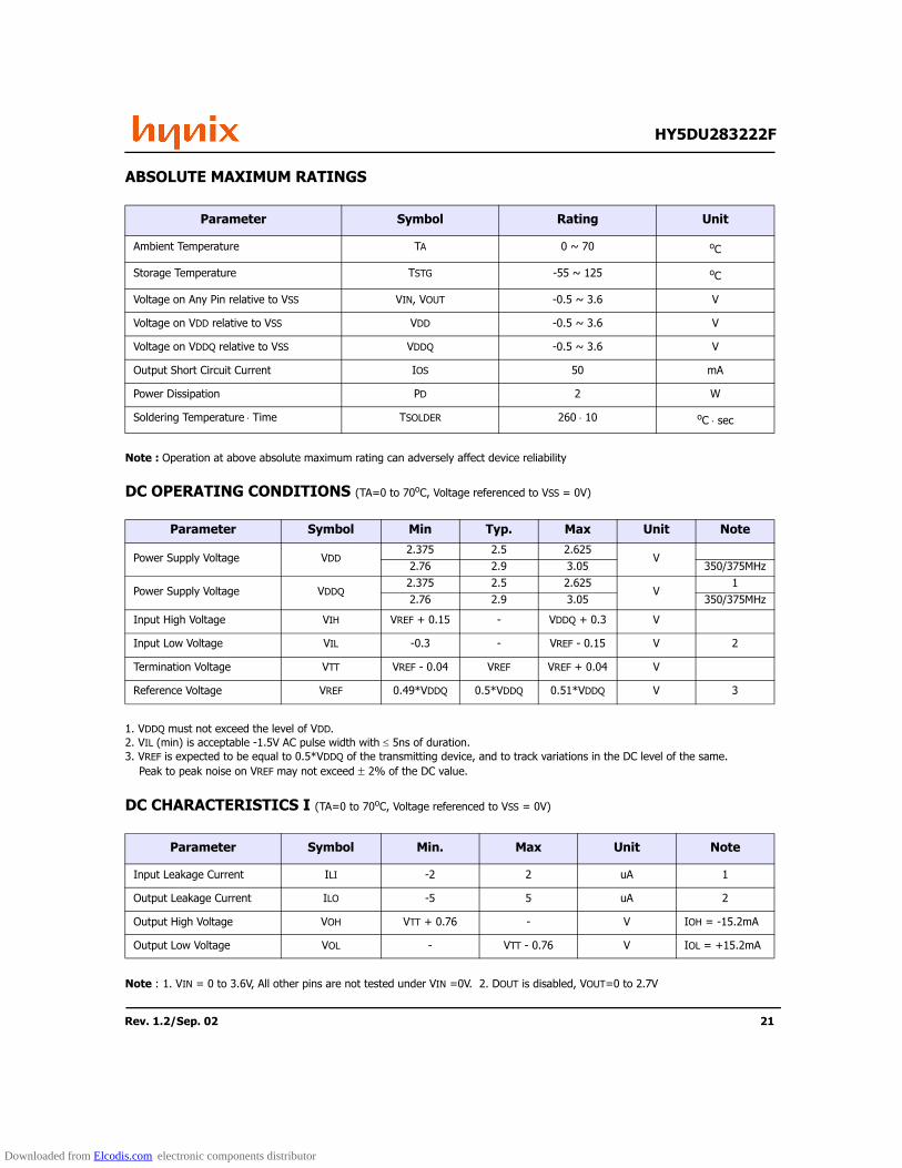
ABSOLUTE MAXIMUM RATINGS
Note : Operation at above absolute maximum rating can adversely affect device reliability
DC OPERATING CONDITIONS (TA=0 to 70oC, Voltage referenced to VSS = 0V)
1. VDDQ must not exceed the level of VDD.2. VIL (min) is acceptable -1.5V AC pulse width with ≤ 5ns of duration. 3. VREF is expected to be equal to 0.5*VDDQ of the transmitting device, and to track variations in the DC level of the same. Peak to peak noise on VREF may not exceed ± 2% of the DC value.
DC CHARACTERISTICS I (TA=0 to 70oC, Voltage referenced to VSS = 0V)
Note : 1. VIN = 0 to 3.6V, All other pins are not tested under VIN =0V. 2. DOUT is disabled, VOUT=0 to 2.7V
Parameter Symbol Rating Unit
Ambient Temperature TA 0 ~ 70 oC
Storage Temperature TSTG -55 ~ 125 oC
Voltage on Any Pin relative to VSS VIN, VOUT -0.5 ~ 3.6 V
Voltage on VDD relative to VSS VDD -0.5 ~ 3.6 V
Voltage on VDDQ relative to VSS VDDQ -0.5 ~ 3.6 V
Output Short Circuit Current IOS 50 mA
Power Dissipation PD 2 W
Soldering Temperature ⋅ Time TSOLDER 260 ⋅ 10 oC ⋅ sec
Parameter Symbol Min Typ. Max Unit Note
Power Supply Voltage VDD2.375 2.5 2.625
V2.76 2.9 3.05 350/375MHz
Power Supply Voltage VDDQ2.375 2.5 2.625
V1
2.76 2.9 3.05 350/375MHz
Input High Voltage VIH VREF + 0.15 - VDDQ + 0.3 V
Input Low Voltage VIL -0.3 - VREF - 0.15 V 2
Termination Voltage VTT VREF - 0.04 VREF VREF + 0.04 V
Reference Voltage VREF 0.49*VDDQ 0.5*VDDQ 0.51*VDDQ V 3
Parameter Symbol Min. Max Unit Note
Input Leakage Current ILI -2 2 uA 1
Output Leakage Current ILO -5 5 uA 2
Output High Voltage VOH VTT + 0.76 - V IOH = -15.2mA
Output Low Voltage VOL - VTT - 0.76 V IOL = +15.2mA
Downloaded from Elcodis.com electronic components distributor
Rev. 1.2/Sep. 02 22
HY5DU283222F
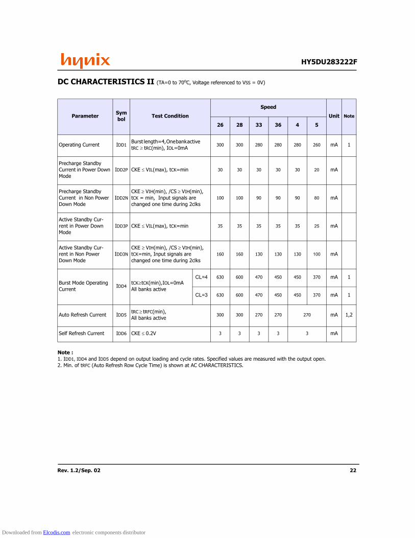
DC CHARACTERISTICS II (TA=0 to 70oC, Voltage referenced to VSS = 0V)
Note : 1. IDD1, IDD4 and IDD5 depend on output loading and cycle rates. Specified values are measured with the output open.2. Min. of tRFC (Auto Refresh Row Cycle Time) is shown at AC CHARACTERISTICS.
Parameter Symbol Test Condition
Speed
Unit Note
26 28 33 36 4 5
Operating Current IDD1Burst length=4, One bank active tRC ≥ tRC(min), IOL=0mA
300 300 280 280 280 260 mA 1
Precharge Standby Current in Power Down Mode
IDD2P CKE ≤ VIL(max), tCK=min 30 30 30 30 30 20 mA
Precharge Standby Current in Non Power Down Mode
IDD2NCKE ≥ VIH(min), /CS ≥ VIH(min), tCK = min, Input signals are changed one time during 2clks
100 100 90 90 90 80 mA
Active Standby Cur-rent in Power Down Mode
IDD3P CKE ≤ VIL(max), tCK=min 35 35 35 35 35 25 mA
Active Standby Cur-rent in Non Power Down Mode
IDD3NCKE ≥ VIH(min), /CS ≥ VIH(min), tCK=min, Input signals are changed one time during 2clks
160 160 130 130 130 100 mA
Burst Mode Operating Current
IDD4tCK ≥ tCK(min), IOL=0mA All banks active
CL=4 630 600 470 450 450 370 mA 1
CL=3 630 600 470 450 450 370 mA 1
Auto Refresh Current IDD5tRC ≥ tRFC(min), All banks active
300 300 270 270 270 mA 1,2
Self Refresh Current IDD6 CKE ≤ 0.2V 3 3 3 3 3 mA
Downloaded from Elcodis.com electronic components distributor
Rev. 1.2/Sep. 02 23
HY5DU283222F
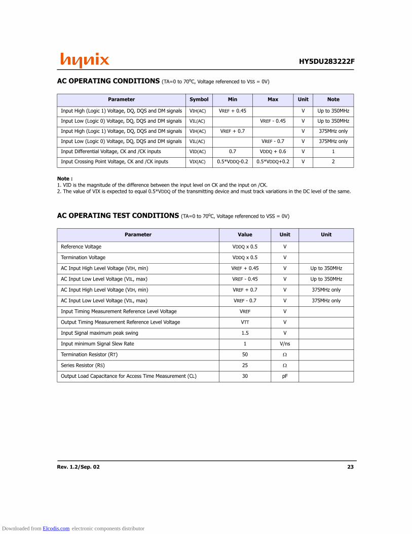
AC OPERATING CONDITIONS (TA=0 to 70oC, Voltage referenced to VSS = 0V)
Note : 1. VID is the magnitude of the difference between the input level on CK and the input on /CK.2. The value of VIX is expected to equal 0.5*VDDQ of the transmitting device and must track variations in the DC level of the same.
AC OPERATING TEST CONDITIONS (TA=0 to 70oC, Voltage referenced to VSS = 0V)
Parameter Symbol Min Max Unit Note
Input High (Logic 1) Voltage, DQ, DQS and DM signals VIH(AC) VREF + 0.45 V Up to 350MHz
Input Low (Logic 0) Voltage, DQ, DQS and DM signals VIL(AC) VREF - 0.45 V Up to 350MHz
Input High (Logic 1) Voltage, DQ, DQS and DM signals VIH(AC) VREF + 0.7 V 375MHz only
Input Low (Logic 0) Voltage, DQ, DQS and DM signals VIL(AC) VREF - 0.7 V 375MHz only
Input Differential Voltage, CK and /CK inputs VID(AC) 0.7 VDDQ + 0.6 V 1
Input Crossing Point Voltage, CK and /CK inputs VIX(AC) 0.5*VDDQ-0.2 0.5*VDDQ+0.2 V 2
Parameter Value Unit Unit
Reference Voltage VDDQ x 0.5 V
Termination Voltage VDDQ x 0.5 V
AC Input High Level Voltage (VIH, min) VREF + 0.45 V Up to 350MHz
AC Input Low Level Voltage (VIL, max) VREF - 0.45 V Up to 350MHz
AC Input High Level Voltage (VIH, min) VREF + 0.7 V 375MHz only
AC Input Low Level Voltage (VIL, max) VREF - 0.7 V 375MHz only
Input Timing Measurement Reference Level Voltage VREF V
Output Timing Measurement Reference Level Voltage VTT V
Input Signal maximum peak swing 1.5 V
Input minimum Signal Slew Rate 1 V/ns
Termination Resistor (RT) 50 Ω
Series Resistor (RS) 25 Ω
Output Load Capacitance for Access Time Measurement (CL) 30 pF
Downloaded from Elcodis.com electronic components distributor
Rev. 1.2/Sep. 02 24
HY5DU283222F
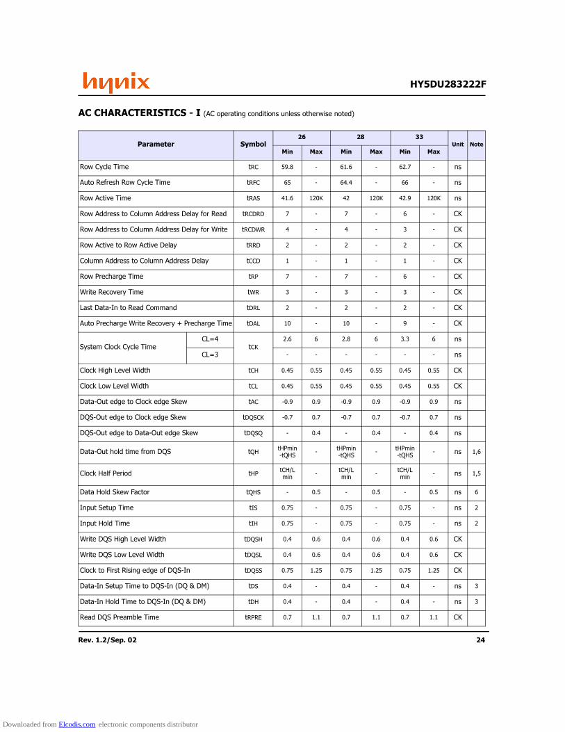
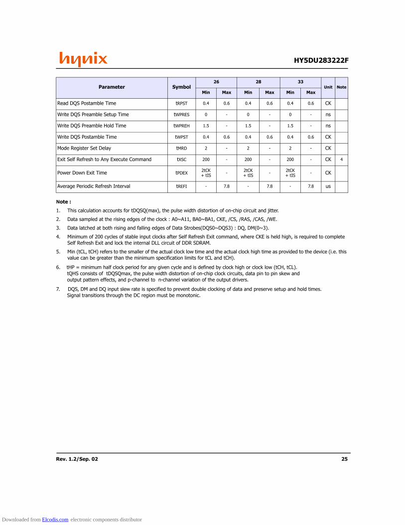
AC CHARACTERISTICS - I (AC operating conditions unless otherwise noted)
Parameter Symbol26 28 33
Unit NoteMin Max Min Max Min Max
Row Cycle Time tRC 59.8 - 61.6 - 62.7 - ns
Auto Refresh Row Cycle Time tRFC 65 - 64.4 - 66 - ns
Row Active Time tRAS 41.6 120K 42 120K 42.9 120K ns
Row Address to Column Address Delay for Read tRCDRD 7 - 7 - 6 - CK
Row Address to Column Address Delay for Write tRCDWR 4 - 4 - 3 - CK
Row Active to Row Active Delay tRRD 2 - 2 - 2 - CK
Column Address to Column Address Delay tCCD 1 - 1 - 1 - CK
Row Precharge Time tRP 7 - 7 - 6 - CK
Write Recovery Time tWR 3 - 3 - 3 - CK
Last Data-In to Read Command tDRL 2 - 2 - 2 - CK
Auto Precharge Write Recovery + Precharge Time tDAL 10 - 10 - 9 - CK
System Clock Cycle TimeCL=4
tCK2.6 6 2.8 6 3.3 6 ns
CL=3 - - - - - - ns
Clock High Level Width tCH 0.45 0.55 0.45 0.55 0.45 0.55 CK
Clock Low Level Width tCL 0.45 0.55 0.45 0.55 0.45 0.55 CK
Data-Out edge to Clock edge Skew tAC -0.9 0.9 -0.9 0.9 -0.9 0.9 ns
DQS-Out edge to Clock edge Skew tDQSCK -0.7 0.7 -0.7 0.7 -0.7 0.7 ns
DQS-Out edge to Data-Out edge Skew tDQSQ - 0.4 - 0.4 - 0.4 ns
Data-Out hold time from DQS tQH tHPmin-tQHS - tHPmin
-tQHS - tHPmin-tQHS - ns 1,6
Clock Half Period tHP tCH/Lmin - tCH/L
min - tCH/Lmin - ns 1,5
Data Hold Skew Factor tQHS - 0.5 - 0.5 - 0.5 ns 6
Input Setup Time tIS 0.75 - 0.75 - 0.75 - ns 2
Input Hold Time tIH 0.75 - 0.75 - 0.75 - ns 2
Write DQS High Level Width tDQSH 0.4 0.6 0.4 0.6 0.4 0.6 CK
Write DQS Low Level Width tDQSL 0.4 0.6 0.4 0.6 0.4 0.6 CK
Clock to First Rising edge of DQS-In tDQSS 0.75 1.25 0.75 1.25 0.75 1.25 CK
Data-In Setup Time to DQS-In (DQ & DM) tDS 0.4 - 0.4 - 0.4 - ns 3
Data-In Hold Time to DQS-In (DQ & DM) tDH 0.4 - 0.4 - 0.4 - ns 3
Read DQS Preamble Time tRPRE 0.7 1.1 0.7 1.1 0.7 1.1 CK
Downloaded from Elcodis.com electronic components distributor
Rev. 1.2/Sep. 02 25
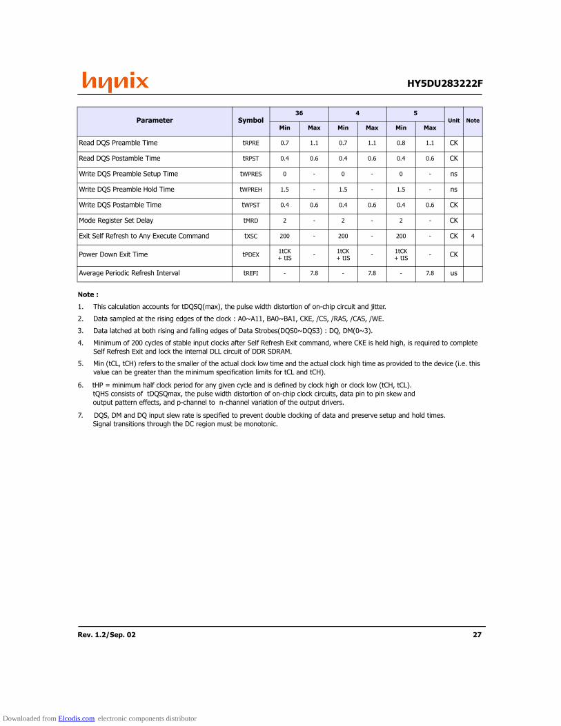
HY5DU283222F
Note :
1. This calculation accounts for tDQSQ(max), the pulse width distortion of on-chip circuit and jitter.
2. Data sampled at the rising edges of the clock : A0~A11, BA0~BA1, CKE, /CS, /RAS, /CAS, /WE.
3. Data latched at both rising and falling edges of Data Strobes(DQS0~DQS3) : DQ, DM(0~3).
4. Minimum of 200 cycles of stable input clocks after Self Refresh Exit command, where CKE is held high, is required to complete Self Refresh Exit and lock the internal DLL circuit of DDR SDRAM.
5. Min (tCL, tCH) refers to the smaller of the actual clock low time and the actual clock high time as provided to the device (i.e. this value can be greater than the minimum specification limits for tCL and tCH).
6. tHP = minimum half clock period for any given cycle and is defined by clock high or clock low (tCH, tCL). tQHS consists of tDQSQmax, the pulse width distortion of on-chip clock circuits, data pin to pin skew and output pattern effects, and p-channel to n-channel variation of the output drivers.
7. DQS, DM and DQ input slew rate is specified to prevent double clocking of data and preserve setup and hold times. Signal transitions through the DC region must be monotonic.
Read DQS Postamble Time tRPST 0.4 0.6 0.4 0.6 0.4 0.6 CK
Write DQS Preamble Setup Time tWPRES 0 - 0 - 0 - ns
Write DQS Preamble Hold Time tWPREH 1.5 - 1.5 - 1.5 - ns
Write DQS Postamble Time tWPST 0.4 0.6 0.4 0.6 0.4 0.6 CK
Mode Register Set Delay tMRD 2 - 2 - 2 - CK
Exit Self Refresh to Any Execute Command tXSC 200 - 200 - 200 - CK 4
Power Down Exit Time tPDEX 2tCK+ tIS - 2tCK
+ tIS - 2tCK+ tIS - CK
Average Periodic Refresh Interval tREFI - 7.8 - 7.8 - 7.8 us
Parameter Symbol26 28 33
Unit NoteMin Max Min Max Min Max
Downloaded from Elcodis.com electronic components distributor
Rev. 1.2/Sep. 02 26
HY5DU283222F
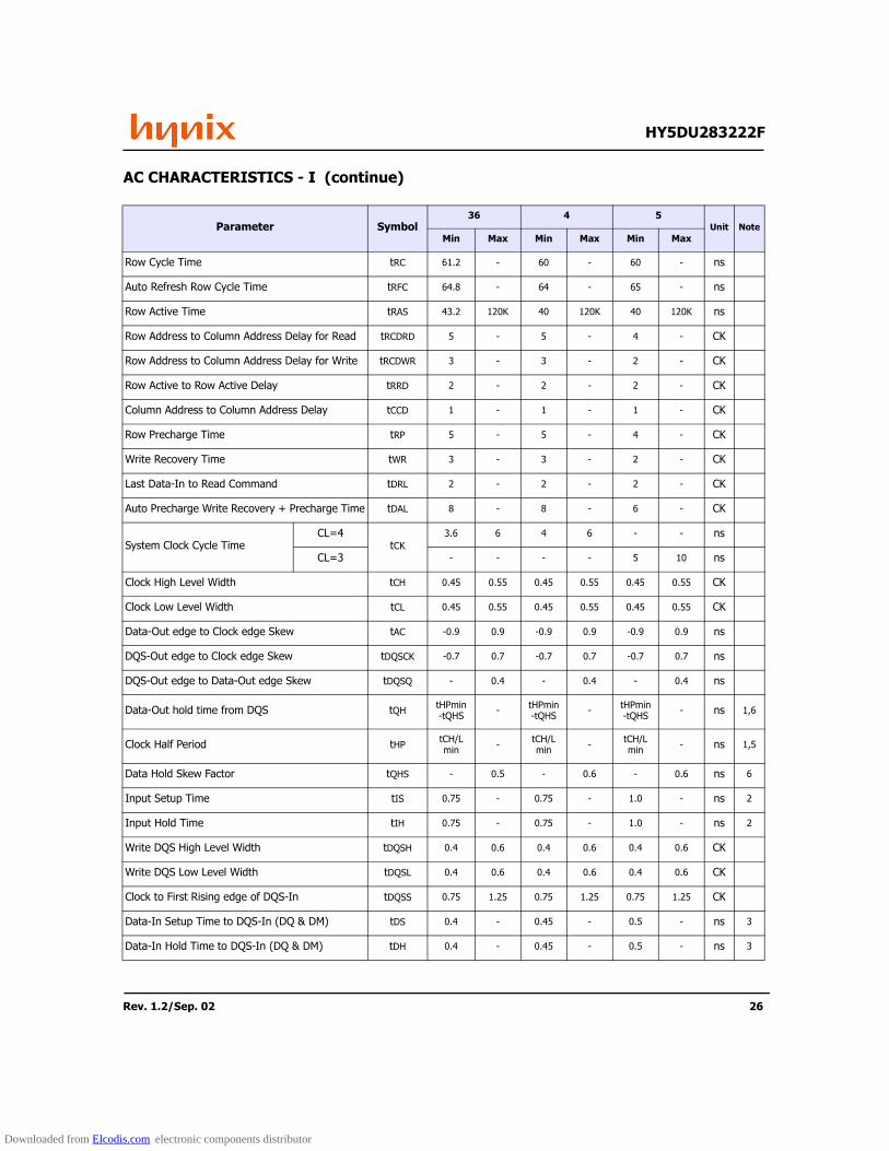
AC CHARACTERISTICS - I (continue)
Parameter Symbol36 4 5
Unit NoteMin Max Min Max Min Max
Row Cycle Time tRC 61.2 - 60 - 60 - ns
Auto Refresh Row Cycle Time tRFC 64.8 - 64 - 65 - ns
Row Active Time tRAS 43.2 120K 40 120K 40 120K ns
Row Address to Column Address Delay for Read tRCDRD 5 - 5 - 4 - CK
Row Address to Column Address Delay for Write tRCDWR 3 - 3 - 2 - CK
Row Active to Row Active Delay tRRD 2 - 2 - 2 - CK
Column Address to Column Address Delay tCCD 1 - 1 - 1 - CK
Row Precharge Time tRP 5 - 5 - 4 - CK
Write Recovery Time tWR 3 - 3 - 2 - CK
Last Data-In to Read Command tDRL 2 - 2 - 2 - CK
Auto Precharge Write Recovery + Precharge Time tDAL 8 - 8 - 6 - CK
System Clock Cycle TimeCL=4
tCK3.6 6 4 6 - - ns
CL=3 - - - - 5 10 ns
Clock High Level Width tCH 0.45 0.55 0.45 0.55 0.45 0.55 CK
Clock Low Level Width tCL 0.45 0.55 0.45 0.55 0.45 0.55 CK
Data-Out edge to Clock edge Skew tAC -0.9 0.9 -0.9 0.9 -0.9 0.9 ns
DQS-Out edge to Clock edge Skew tDQSCK -0.7 0.7 -0.7 0.7 -0.7 0.7 ns
DQS-Out edge to Data-Out edge Skew tDQSQ - 0.4 - 0.4 - 0.4 ns
Data-Out hold time from DQS tQH tHPmin-tQHS - tHPmin
-tQHS - tHPmin-tQHS - ns 1,6
Clock Half Period tHP tCH/Lmin - tCH/L
min - tCH/Lmin - ns 1,5
Data Hold Skew Factor tQHS - 0.5 - 0.6 - 0.6 ns 6
Input Setup Time tIS 0.75 - 0.75 - 1.0 - ns 2
Input Hold Time tIH 0.75 - 0.75 - 1.0 - ns 2
Write DQS High Level Width tDQSH 0.4 0.6 0.4 0.6 0.4 0.6 CK
Write DQS Low Level Width tDQSL 0.4 0.6 0.4 0.6 0.4 0.6 CK
Clock to First Rising edge of DQS-In tDQSS 0.75 1.25 0.75 1.25 0.75 1.25 CK
Data-In Setup Time to DQS-In (DQ & DM) tDS 0.4 - 0.45 - 0.5 - ns 3
Data-In Hold Time to DQS-In (DQ & DM) tDH 0.4 - 0.45 - 0.5 - ns 3
Downloaded from Elcodis.com electronic components distributor
Rev. 1.2/Sep. 02 27
HY5DU283222F
Note :
1. This calculation accounts for tDQSQ(max), the pulse width distortion of on-chip circuit and jitter.
2. Data sampled at the rising edges of the clock : A0~A11, BA0~BA1, CKE, /CS, /RAS, /CAS, /WE.
3. Data latched at both rising and falling edges of Data Strobes(DQS0~DQS3) : DQ, DM(0~3).
4. Minimum of 200 cycles of stable input clocks after Self Refresh Exit command, where CKE is held high, is required to complete Self Refresh Exit and lock the internal DLL circuit of DDR SDRAM.
5. Min (tCL, tCH) refers to the smaller of the actual clock low time and the actual clock high time as provided to the device (i.e. this value can be greater than the minimum specification limits for tCL and tCH).
6. tHP = minimum half clock period for any given cycle and is defined by clock high or clock low (tCH, tCL). tQHS consists of tDQSQmax, the pulse width distortion of on-chip clock circuits, data pin to pin skew and output pattern effects, and p-channel to n-channel variation of the output drivers.
7. DQS, DM and DQ input slew rate is specified to prevent double clocking of data and preserve setup and hold times. Signal transitions through the DC region must be monotonic.
Read DQS Preamble Time tRPRE 0.7 1.1 0.7 1.1 0.8 1.1 CK
Read DQS Postamble Time tRPST 0.4 0.6 0.4 0.6 0.4 0.6 CK
Write DQS Preamble Setup Time tWPRES 0 - 0 - 0 - ns
Write DQS Preamble Hold Time tWPREH 1.5 - 1.5 - 1.5 - ns
Write DQS Postamble Time tWPST 0.4 0.6 0.4 0.6 0.4 0.6 CK
Mode Register Set Delay tMRD 2 - 2 - 2 - CK
Exit Self Refresh to Any Execute Command tXSC 200 - 200 - 200 - CK 4
Power Down Exit Time tPDEX 1tCK+ tIS - 1tCK
+ tIS - 1tCK+ tIS - CK
Average Periodic Refresh Interval tREFI - 7.8 - 7.8 - 7.8 us
Parameter Symbol36 4 5
Unit NoteMin Max Min Max Min Max
Downloaded from Elcodis.com electronic components distributor
Rev. 1.2/Sep. 02 28
HY5DU283222F
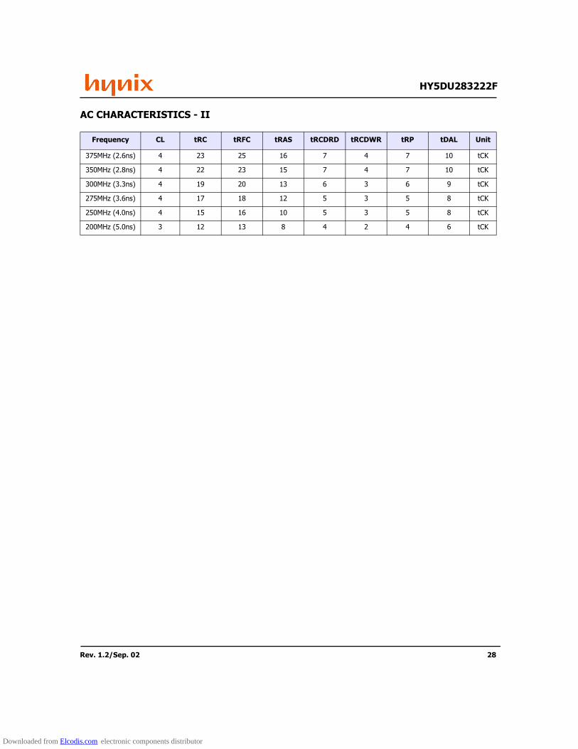
AC CHARACTERISTICS - II
Frequency CL tRC tRFC tRAS tRCDRD tRCDWR tRP tDAL Unit
375MHz (2.6ns) 4 23 25 16 7 4 7 10 tCK
350MHz (2.8ns) 4 22 23 15 7 4 7 10 tCK
300MHz (3.3ns) 4 19 20 13 6 3 6 9 tCK
275MHz (3.6ns) 4 17 18 12 5 3 5 8 tCK
250MHz (4.0ns) 4 15 16 10 5 3 5 8 tCK
200MHz (5.0ns) 3 12 13 8 4 2 4 6 tCK
Downloaded from Elcodis.com electronic components distributor
Rev. 1.2/Sep. 02 29
HY5DU283222F
CAPACITANCE (TA=25oC, f=1MHz )
Note : 1. VDD = min. to max., VDDQ = 2.3V to 2.7V, VODC = VDDQ/2, VOpeak-to-peak = 0.2V2. Pins not under test are tied to GND.3. These values are guaranteed by design and are tested on a sample basis only.
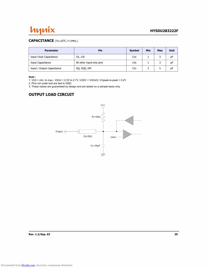
OUTPUT LOAD CIRCUIT
Parameter Pin Symbol Min Max Unit
Input Clock Capacitance CK, /CK CCK 1 3 pF
Input Capacitance All other input-only pins CIN 1 3 pF
Input / Output Capacitance DQ, DQS, DM CIO 3 5 pF
VREF
VTT
RT=50Ω
Zo=50Ω
CL=30pF
Output
Downloaded from Elcodis.com electronic components distributor
Rev. 1.2/Sep. 02 30
HY5DU283222F
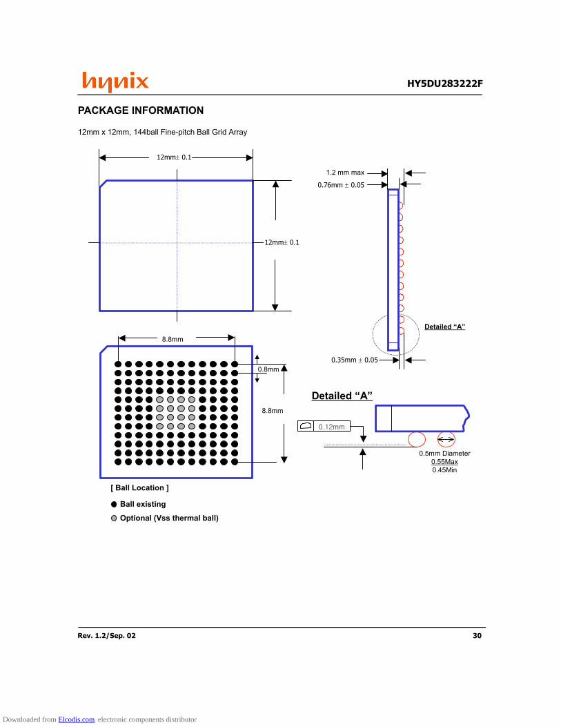
PACKAGE INFORMATION
12mm x 12mm, 144ball Fine-pitch Ball Grid Array
0.76mm ± 0.05
1.2 mm max
Detailed “A”
Detailed “A”
0.5mm Diameter0.55Max0.45Min
0.12mm
Ball existing
Optional (Vss thermal ball)
[ Ball Location ]
12mm± 0.1
12mm± 0.1
0.8mm
8.8mm
8.8mm
0.35mm ± 0.05
Downloaded from Elcodis.com electronic components distributor


![299 128m .]p 399B 128m .]p 399B 9B a-AS a-kl nr-Jb 158; 498; 798Å199Å278Å 4480435b; Created Date 5/7/2013 4:41:55 PM](https://img.pdfslide.us/doc/110x75/5aabef6b7f8b9aa9488c93d7/299-128m-p-128m-p-399b-9b-a-as-a-kl-nr-jb-158-498-798199278-4480435b-created.jpg)