Embed Size (px)
Citation preview

1.25 GHz Dual Integrated DCL with PPMU, Level Setting DACs, and On-Chip Calibration Registers
Data Sheet ADATE320
Rev. B Document Feedback Information furnished by Analog Devices is believed to be accurate and reliable. However, no responsibility is assumed by Analog Devices for its use, nor for any infringements of patents or other rights of third parties that may result from its use. Specifications subject to change without notice. No license is granted by implication or otherwise under any patent or patent rights of Analog Devices. Trademarks and registered trademarks are the property of their respective owners.
One Technology Way, P.O. Box 9106, Norwood, MA 02062-9106, U.S.A. Tel: 781.329.4700 ©2015–2016 Analog Devices, Inc. All rights reserved. Technical Support www.analog.com
FEATURES 1.25 GHz, 2.5 Gbps data rate 3-level driver with high-Z and reflection clamps Window and differential comparators ±25 mA active load Per pin parametric measurement unit (PMU) with a −1.5 V to
+4.5 V range Low leakage mode (typically <5 nA) Integrated 16-bit DACs with offset and gain correction 1.2 W power dissipation per channel (ADATE320) 1.3 W power dissipation per channel (ADATE320-1) Driver
Voltage range: −1.5 V to +4.5 V Precision trimmed termination: 50.0 Ω Unterminated swing: 50 mV minimum to 6.0 V maximum 400 ps minimum pulse width, 1.0 V programmed swing 25 ps deterministic jitter
Comparator Differential and single-ended window modes 100 ps equivalent input rise/fall time (ERT/EFT) 250 mV current mode logic (CML) outputs (ADATE320) 400 mV CML outputs (ADATE320-1)
Load Per pin PMU (PPMU)
Force voltage/compliance range: −1.5 V to +4.5 V 5 current ranges
±40 mA, ±1 mA, ±100 μA, ±10 µA, ±2 µA Dedicated go/no-go comparators
DC levels Fully integrated and dedicated 16-bit DACs On-chip gain and offset calibration registers with
automatic add/multiply function 84-lead, 10 mm × 10 mm LFCSP (0.4 mm pitch)
APPLICATIONS Automatic test equipment (ATE) Semiconductor/board test systems Instrumentation and characterization equipment
GENERAL DESCRIPTION The ADATE320 is a complete, single-chip ATE solution that performs the pin electronics functions of a driver, comparator, and active load (DCL), and a four quadrant per pin parametric measurement unit (PPMU). Dedicated 16-bit digital-to-analog converters (DACs) with on-chip calibration registers provide all the necessary dc levels for operation of the device.
The driver features three active modes: high, low, and terminate, as well as a high impedance inhibit state. The inhibit state, in conjunction with the integrated dynamic clamps, facilitates significant attenuation of transmission line reflections when the driver is not actively terminating the line. The open-circuit drive capability is −1.5 V to +4.5 V to accommodate a standard range of ATE and instrumentation applications.
The ADATE320 can be used as a dual, single-ended pin electronics channel or as a single differential channel. In addition to per channel high speed window comparators, the ADATE320 provides a programmable threshold differential comparator for differential ATE applications.
All dc levels for DCL and PPMU functions are generated by dedicated, on-chip, 16-bit DACs. To facilitate the programming of accurate levels, the ADATE320 includes an integrated calibration function to correct for the gain and offset errors of each functional block. Correction coefficients can be stored on chip, and any values written to the DACs adjust automatically using the appropriate correction factors.
The ADATE320 uses a serial programmable interface (SPI) bus to program all functional blocks, DACs, and on-chip calibration constants. It also has an on-chip temperature sensor and overvolt-age/undervoltage fault clamps that monitor and report the device temperature and any output pin or transient PPMU voltage faults that may occur during operation.
The ADATE320 is available in two options. The standard option has high speed comparator outputs with 250 mV output swing. The ADATE320-1 has 400 mV output swing. See the Ordering Guide for more information.

ADATE320 Data Sheet
Rev. B | Page 2 of 82
TABLE OF CONTENTS Features .............................................................................................. 1 Applications ....................................................................................... 1 General Description ......................................................................... 1 Revision History ............................................................................... 2 Functional Block Diagram .............................................................. 3 Specifications ..................................................................................... 4
Electrical Specifications ............................................................... 4 Driver Specifications .................................................................... 5 Reflection Clamp Specifications ................................................. 7 Normal Window Comparator (NWC) Specifications ............. 8 Differential Mode Comparator (DMC) Specifications ......... 10 Active Load Specifications ........................................................ 11 PPMU Specifications ................................................................. 13 PPMU Go/No-Go Comparators Specifications ..................... 18 PPMU External Sense Pins Specifications .............................. 18 VREF, VREFGND, and DUTGND Reference Input Pins Specifications .............................................................................. 19 Temperature Monitor Specifications ....................................... 19 Alarm Functions Specifications................................................ 19 Serial Programmable Interface (SPI) Specifications .............. 20 SPI Timing Specifications ......................................................... 20 SPI Timing Diagrams ................................................................. 21
Absolute Maximum Ratings .......................................................... 25
Thermal Characteristics ............................................................ 25 Explanation of Test Levels ......................................................... 25 ESD Caution................................................................................ 25 User Information and Truth Tables ......................................... 26
Pin Configuration and Function Descriptions ........................... 28 Typical Performance Characteristics ........................................... 30 Theory of Operation ...................................................................... 50
Serial Programmable Interface (SPI) ....................................... 50 Level Setting DACs .................................................................... 52 Alarm Functions ......................................................................... 59
Applications Information .............................................................. 62 Power Supply, Grounding, and Typical Decoupling Strategy....................................................................................................... 62 Power Supply Sequencing ......................................................... 64
Detailed Functional Block Diagrams ........................................... 65 SPI Register Memory Map and Details ....................................... 71
Memory Map .............................................................................. 71 Register Details ........................................................................... 74
Default Test Conditions ................................................................. 80 External Components .................................................................... 81 Outline Dimensions ....................................................................... 82
Ordering Guide .......................................................................... 82
REVISION HISTORY 9/2016—Rev. A to Rev. B Changes to Time Constant 1 Parameter and Time Constant 2 Parameter, Table 2 ............................................................................. 7 Changes to IOx Offset Parameter, and IOHx Offset Parameter, Table 6 ........................................................................... 11 Change to AGND Pin Number Column ..................................... 29 Change to SPI Reset Sequence and the RST Pin Section .......... 50 Changes to the SPI Clock Cycles and BUSY Pin Section .......... 51 Changes to Table 24 ........................................................................ 54 Changes to Figure 137 .................................................................... 65 10/2015—Revision A: Initial Version

Data Sheet ADATE320
Rev. B | Page 3 of 82
FUNCTIONAL BLOCK DIAGRAM
+
–
VIL0VIT0/VCOM0
VIH0
VOL0
DUT0
VTTD0
CMPH0/CMPH0
CMPL0/CMPL0
NWC
NWC
DIFF
DRIVER
LOAD
COMPARATOR
50Ω
PPMU_S0
THERMPPMU_M0
PMU
CHANNEL 0
S F
OUTPMU0PCH0PCL0
VCH0VCL0
OVDH
OVDL
TO ALARM(HIGH/LOW
VOLTAGE FAULT)PPMU_CMP0
VTTC0
DA
T1R
CV1
(FR
OM
CH
AN
NEL
1)
TO ALARM(HIGH/LOW
CLAMP FAULT)
POH0
POL0
MUX
OVERVOLTAGE
MUX
MUX
MUX
CHANNEL 1(SAME AS CHANNEL 0 EXCEPT WHERE NOTED ABOVE)
COMMON
SPI
RST
MUX
TEMPSENSORVTHERM
ALARM ALARM VDD
AGND
PGND
VEE
DGND
(FR
OM
DU
T)
DA
T0R
CV0
(TO
CH
AN
NEL
1)
VCC
SDO
SCLKSDI
DAT0/DAT0
RCV0/RCV0
GAIN/OFFSETCORRECTION 2 × 16
16-BIT DACs
BUSY
CS
CH0 ONLY
IOH0
IOL0
PPMUGO/NO-GO
50Ω
50Ω
VOH0
1216
0-00
1
Figure 1.
ADATE320 Data Sheet
Rev. B | Page 4 of 82
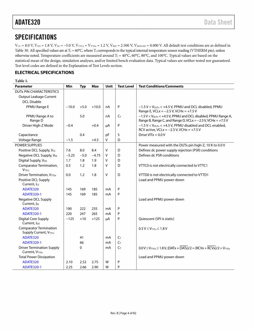
SPECIFICATIONS VCC = 8.0 V, VDD = 1.8 V, VEE = −5.0 V, VTTCx = VTTDx = 1.2 V, VREF = 2.500 V, VREFGND = 0.000 V. All default test conditions are as defined in Table 30. All specified values are at TJ = 60°C, where TJ corresponds to the typical internal temperature sensor reading (VTHERM pin), unless otherwise noted. Temperature coefficients are measured around TJ = 40°C, 60°C, 80°C, and 100°C. Typical values are based on the statistical mean of the design, simulation analyses, and/or limited bench evaluation data. Typical values are neither tested nor guaranteed. Test level codes are defined in the Explanation of Test Levels section.
ELECTRICAL SPECIFICATIONS
Table 1. Parameter Min Typ Max Unit Test Level Test Conditions/Comments DUTx PIN CHARACTERISTICS
Output Leakage Current DCL Disable
PPMU Range E −10.0 +5.0 +10.0 nA P −1.5 V < VDUTx < +4.5 V, PPMU and DCL disabled, PPMU Range E, VCLx = −2.5 V, VCHx = +7.5 V
PPMU Range A to Range D
5.0 nA CT −1.5 V < VDUTx < +4.5 V, PPMU and DCL disabled, PPMU Range A, Range B, Range C, and Range D, VCLx = −2.5 V, VCHx = +7.5 V
Driver High-Z Mode −0.4 +0.4 µA P −1.5 V < VDUTx < +4.5 V, PPMU disabled and DCL enabled, RCV active, VCLx = −2.5 V, VCHx = +7.5 V
Capacitance 0.4 pF S Drive VITx = 0.0 V Voltage Range −1.5 +4.5 V D
POWER SUPPLIES Power measured with the DUTx pin high-Z, 10 K to 0.0 V Positive DCL Supply, VCC 7.6 8.0 8.4 V D Defines dc power supply rejection (PSR) conditions Negative DCL Supply, VEE −5.25 −5.0 −4.75 V D Defines dc PSR conditions Digital Supply, VDD 1.7 1.8 1.9 V D Comparator Termination,
VTTCx 0.5 1.2 1.8 V D VTTC0 is not electrically connected to VTTC1
Driver Termination, VTTDx 0.0 1.2 1.8 V D VTTD0 is not electrically connected to VTTD1 Positive DCL Supply
Current, ICC Load and PPMU power-down
ADATE320 145 169 185 mA P ADATE320-1 145 169 185 mA P
Negative DCL Supply Current, IEE
Load and PPMU power-down
ADATE320 190 222 235 mA P ADATE320-1 220 247 265 mA P
Digital Core Supply Current, IDD
−125 +10 +125 μA P Quiescent (SPI is static)
Comparator Termination Supply Current, VTTCx
0.5 V ≤ VTTCx ≤ 1.8 V
ADATE320 41 mA CT ADATE320-1 66 mA CT
Driver Termination Supply Current, VTTDx
0 mA CT 0.0 V ≤ VTTDx ≤ 1.8 V, (DATx + DATx)/2 = (RCVx + RCVx)/2 = VTTDx
Total Power Dissipation Load and PPMU power-down ADATE320 2.10 2.52 2.75 W P ADATE320-1 2.25 2.66 2.90 W P
Data Sheet ADATE320
Rev. B | Page 5 of 82
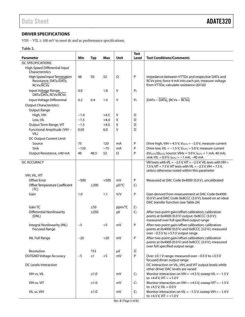
DRIVER SPECIFICATIONS VIH − VIL ≥ 100 mV to meet dc and ac performance specifications.
Table 2.
Parameter Min Typ Max Unit Test Level Test Conditions/Comments
DC SPECIFICATIONS High Speed Differential Input
Characteristics
High Speed Input Termination Resistance: DATx/DATx, RCVx/ RCVx
48 50 52 Ω P Impedance between VTTDx and respective DATx and RCVx pins; force 4 mA into each pin, measure voltage from VTTDx; calculate resistance (∆V/∆I)
Input Voltage Range: DATx/DATx, RCVx/RCVx
0.0 1.8 V PF
Input Voltage Differential 0.2 0.4 1.0 V PF |DATx − DATx|, |RCVx − RCVx|
Output Characteristics Output Range
High, VIH −1.4 +4.5 V D Low, VIL −1.5 +4.4 V D
Output Term Range, VIT −1.5 +4.5 V D Functional Amplitude (VIH −
VIL) 0.05 6.0 V D
DC Output Current Limit Source 75 120 mA P Drive high, VIH = 4.5 V, VDUTx = −2.0 V, measure current Sink −120 −75 mA P Drive low, VIL = −1.5 V, VDUTx = 5.0 V, measure current
Output Resistance, ±40 mA 46 48.5 52 Ω P ∆VDUTx/∆IDUTx; source: VIHx = 3.0 V, IDUTx = 1 mA, 40 mA; sink: VIL = 0.0 V, IDUTx = −1 mA, −40 mA
DC ACCURACY VIH tests with VIL = −2.5 V, VIT = −2.5 V; VIL tests with VIH = 7.5 V, VIT = 7.5 V; VIT tests with VIL = −2.5 V, VIH = 7.5 V, unless otherwise noted within this parameter
VIH, VIL, VIT Offset Error −500 +500 mV P Measured at DAC Code 0x4000 (0.0 V), uncalibrated Offset Temperature Coefficient
(TC) ±200 µV/°C CT
Gain 1.0 1.1 V/V P Gain derived from measurement at DAC Code 0x4000 (0.0 V) and DAC Code 0x8CCC (3.0 V); based on an ideal DAC transfer function (see Table 24)
Gain TC ±50 ppm/°C CT Differential Nonlinearity
(DNL) ±250 µV CT After two-point gain/offset calibration; calibration
points at 0x4000 (0.0 V) output; 0x8CCC (3.0 V); measured over full specified output range
Integral Nonlinearity (INL) Focused Range
−5 +5 mV P After two-point gain/offset calibration; calibration points at 0x4000 (0.0 V) and 0x8CCC (3.0 V); measured over −0.5 V to +3.5 V output range
INL Full Range −20 +20 mV P After two-point gain/offset calibration; calibration points at 0x4000 (0.0 V) and 0x8CCC (3.0 V); measured over full specified output range
Resolution 153 µV D DUTGND Voltage Accuracy −5 ±1 +5 mV P Over ±0.1 V range; measured over −0.5 V to +3.5 V
focused driver output range DC Levels Interaction DC interaction on VIL, VIH, and VIT output levels while
other driver DAC levels are varied VIH vs. VIL ±1.0 mV CT Monitor interaction on VIH = +4.5 V; sweep VIL = −1.5 V
to +4.4 V, VIT = +1.0 V VIH vs. VIT ±1.0 mV CT Monitor interaction on VIH = +4.5 V; sweep VIT = −1.5 V
to +4.5 V, VIL = 0.0 V VIL vs. VIH ±1.0 mV CT Monitor interaction on VIL = −1.5 V; sweep VIH = −1.4 V
to +4.5 V, VIT = +1.0 V

ADATE320 Data Sheet
Rev. B | Page 6 of 82
Parameter Min Typ Max Unit Test Level Test Conditions/Comments
VIL vs. VIT ±1.0 mV CT Monitor interaction on VIL = −1.5 V; sweep VIT = −1.5 V to +4.5 V, VIH = +2.0 V
VIT vs. VIH ±2.0 mV CT Monitor interaction on VIT = 1.0 V; sweep VIH = −1.4 V to +4.5 V, VIL = −1.5 V
VIT vs. VIL ±2.0 mV CT Monitor interaction on VIT = 1.0 V; sweep VIL = −1.5 V to +4.4 V, VIH = +4.5 V
Overall Voltage Accuracy Focused Range
±5 mV CT VIH − VIL ≥ 100 mV; sum of INL, dc interaction, DUTGND and TC errors over ±5°C, after calibration
VIH, VIL, VIT DC PSR +15 mV/V CT Measured at calibration points, see Table 1 for power supply ranges
AC SPECIFICATIONS All ac specifications performed after dc calibration Rise/Fall Times Toggle DATx, VIL = 0.0 V, terminated
0.2 V Programmed Swing tRISE 150 ps CB 20% to 80%, VIH = 0.2 V tFALL 170 ps CB 20% to 80%, VIH = 0.2 V
0.5 V Programmed Swing tRISE 150 ps CB 20% to 80%, VIH = 0.5 V tFALL 170 ps CB 20% to 80%, VIH = 0.5 V
1.0 V Programmed Swing tRISE 150 ps CB 20% to 80%, VIH = 1.0 V tFALL 170 ps CB 20% to 80%, VIH = 1.0 V
2.0 V Programmed Swing tRISE 120 160 230 ps P 20% to 80%, VIH = 2.0 V tFALL 120 180 230 ps P 20% to 80%, VIH = 2.0 V
4.0 V Programmed Swing tRISE 320 ps CB 10% to 90%, VIH = 4.0 V, unterminated tFALL 320 ps CB 10% to 90%, VIH = 4.0 V, unterminated
tRISE to tFALL Mismatch −20 ps CB tRISE − tFALL (20% to 80%) within one channel, VIH = 2.0 V, VIL = 0.0 V, terminated
Trailing Edge Timing Error Toggle DATx Programmed Swing VIL = 0.0 V, terminated, 400 ps ≤ pulse width (PW) ≤ 10 ns
0.2 V ±15 ps CB VIH = 0.2 V 0.5 V ±15 ps CB VIH = 0.5 V 1.0 V ±15 ps CB VIH = 1.0 V 2.0 V ±15 ps CB VIH = 2.0 V
Maximum Toggle Rate Toggle DATx Programmed Swing VIL = 0.0 V, terminated ≤10% amplitude loss
0.2 V 2.8 Gbps CB VIH = 0.2 V 0.5 V 3.2 Gbps CB VIH = 0.5 V 1.0 V 3.2 Gbps CB VIH = 1.0 V 2.0 V 2.8 Gbps CB VIH = 2.0 V
Dynamic Performance Toggle DATx, drive VIL to/from VIH Propagation Delay VIH = 2.0 V, VIL = 0.0 V, terminated
Time 750 ps CB TC 2 ps/°C CT
Delay Matching VIH = 2.0 V, VIL = 0.0 V, terminated Edge to Edge 10 ps CB tLH0 − tHL0; tLH1 − tHL1 Channel to Channel 35 ps CB tLH0 − tLH1; tHL0 − tHL1
Delay Change vs. Duty Cycle ±7 ps CB VIH = 2.0 V, VIL = 0.0 V, terminated, 1 MHz, 5% to 95% Overshoot and Undershoot 50 mV CB VIH = 2.0 V, VIL = 0.0 V, terminated, minimum driver CLC Settling Time (VIH to VIL) Toggle DATx
To Within 3% of Final Value 1 ns CB VIH = 2.0 V, VIL = 0.0 V, from 50% crossing, terminated To Within 1% of Final Value 10 ns CB VIH = 2.0 V, VIL = 0.0 V, from 50% crossing, terminated

Data Sheet ADATE320
Rev. B | Page 7 of 82
Parameter Min Typ Max Unit Test Level Test Conditions/Comments
Dynamic Performance Drive Active to/from VIT Toggle RCVx, VIH = 2.0 V, VIT = 1.0 V, VIL = 0.0 V, terminated
Transition Time 20% to 80% Active to VIT 200 ps CB VIT to Active 170 ps CB
Propagation Delay 1.0 ns CB TC 2 ps/°C CT
Drive Active to/from Inhibit Toggle RCVx, VIH = 1.0 V, VIL = −1.0 V, terminated Transition Time 20% to 80%
Inhibit to Active 250 ps CB Active to Inhibit 850 ps CB
Propagation Delay Inhibit to VIH 2.1 ns CB Inhibit to VIL 2.5 ns CB Matching Inhibit to VIL vs.
Inhibit to VIH 0.4 ns CB
VIH to Inhibit 2.5 ns CB VIL to Inhibit 2.1 ns CB
Input/Output Spike 125 mV p-p CB VIH = 0.0 V, VIL = 0.0 V, terminated, toggle RCVx Cable Loss Compensation (CLC) VIH = 2.0 V, VIL = 0.0 V, terminated
Amplitude 20 % CB Maximum CLC setting Resolution 3 Bits D Time Constant 1 400 ps S Maximum CLC setting Time Constant 2 1.5 ns S Maximum CLC setting
REFLECTION CLAMP SPECIFICATIONS Clamp accuracy specifications apply only when VCHx − VCLx > 0.8 V.
Table 3.
Parameter Min Typ Max Unit Test Level Test Conditions/Comments
VCH Functional Range −0.5 +5.0 V D Offset Error −300 +300 mV P Driver high-Z, sinking 1 mA, measured at DAC Code 0x4000
(0.0 V), uncalibrated Offset TC ±0.25 mV/°C CT Gain 1.0 1.1 V/V P Driver high-Z, sinking 1 mA, gain derived from measurements
at DAC Code 0x4000 (0.0 V) and DAC Code 0x8CCC (3.0 V), based on an ideal DAC transfer function (see Table 24)
Gain TC ±25 ppm/°C CT Resolution 153 µV D DNL ±250 µV CT Driver high-Z, sinking 1 mA, after two-point gain/offset
calibration; calibration points at DAC Code 0x4000 (0.0 V) and DAC Code 0x8CCC (3.0 V), measured over the functional range
INL −20 +20 mV P Driver high-Z, sinking 1 mA, after two-point gain/offset calibration; calibration points at DAC Code 0x4000 (0.0 V) and DAC Code 0x8CCC (3.0 V), measured over the functional range
VCL Functional Range −2.0 +3.5 V D Offset Error −300 +300 mV P Driver high-Z, sourcing 1 mA, measured at DAC Code 0x4000
(0.0 V), uncalibrated Offset TC ±0.25 mV/°C CT

ADATE320 Data Sheet
Rev. B | Page 8 of 82
Parameter Min Typ Max Unit Test Level Test Conditions/Comments
Gain 1.0 1.1 V/V P Drive high-Z, sourcing 1 mA, gain derived from measure-ments at DAC Code 0x4000 (0.0 V) and DAC Code 0x8CCC (3.0 V), based on an ideal DAC transfer function (see Table 24)
Gain TC ±25 ppm/°C CT Resolution 153 µV D DNL ±250 µV CT Drive high-Z, sourcing 1 mA, after two-point gain/offset
calibration; calibration points at DAC Code 0x4000 (0.0 V) and DAC Code 0x8CCC (3.0 V), measured over the functional range
INL −20 +20 mV P Drive high-Z, sourcing 1 mA, after two-point gain/offset calibration; calibration points at DAC Code 0x4000 (0.0 V) and DAC Code 0x8CCC (3.0 V), measured over the functional range
DC CLAMP CURRENT LIMIT Drive high-Z VCHx −105 −60 mA P VCHx = −1.0 V, VCLx = −2.0 V, VDUTx = 4.5 V VCLx +60 +105 mA P VCHx = 5.0 V, VCLx = 4.0 V, VDUTx = −1.5 V
DUTGND VOLTAGE ACCURACY −10 ±2 +10 mV P Over ±0.1 V range, measured at end points of VCHx and VCLx functional range
NORMAL WINDOW COMPARATOR (NWC) SPECIFICATIONS
Table 4.
Parameter Min Typ Max Unit Test Level Test Conditions/Comments
DC SPECIFICATIONS Input Voltage Range −1.5 +4.5 V D Differential Voltage Range ±0.1 ±6.0 V D Input Offset Voltage −250 +250 mV P Measured at DAC Code 0x4000 (0.0 V); uncalibrated
Input Offset Voltage TC ±150 µV/°C CT Gain 1.0 1.1 V/V P Gain derived from measurements at DAC Code 0x4000
(0.0 V) and DAC Code 0x8CCC (3.0 V); based on an ideal DAC transfer function (see Table 24)
Gain TC ±10 ppm/°C CT Threshold Resolution 153 µV D Threshold DNL ±0.25 mV CT Measured over −1.5 V to +4.5 V functional range after
two-point gain/offset calibration; calibration points at DAC Code 0x4000 (0.0 V) and DAC Code 0x8CCC (3.0 V)
Threshold INL After two-point gain/offset calibration; calibration points at DAC Code 0x4000 (0.0 V) and DAC Code 0x8CCC (3.0 V)
Focused Range −5 +5 mV P Measured over −0.5 V to +3.5 V range Full Range −7 +7 mV P Measured over −1.5 V to +4.5 V range
DUTGND Voltage Accuracy −5 ±1 +5 mV P Over ±0.1 V range; measured over −0.5 V to +3.5 V focused NWC input range
Uncertainty Band 10 mV CB VDUTx = 0.0 V, sweep comparator threshold to determine the uncertainty band
Programmable Hysteresis 100 mV CB Hysteresis Resolution 4 Bits D DC PSR ±5 mV/V CT Measured at DAC Code 0x4000 (0.0 V) and DAC Code 0x8CCC
(3.0 V) calibration points Digital Output
Characteristics
Internal Pull-up Resistance to Comparator, VTTCx
46 50 54 Ω P Source 1 mA and 10 mA from the output pin in high state, measure ∆V to calculate resistance; R = ∆V/9 mA; repeat for all output pins
Data Sheet ADATE320
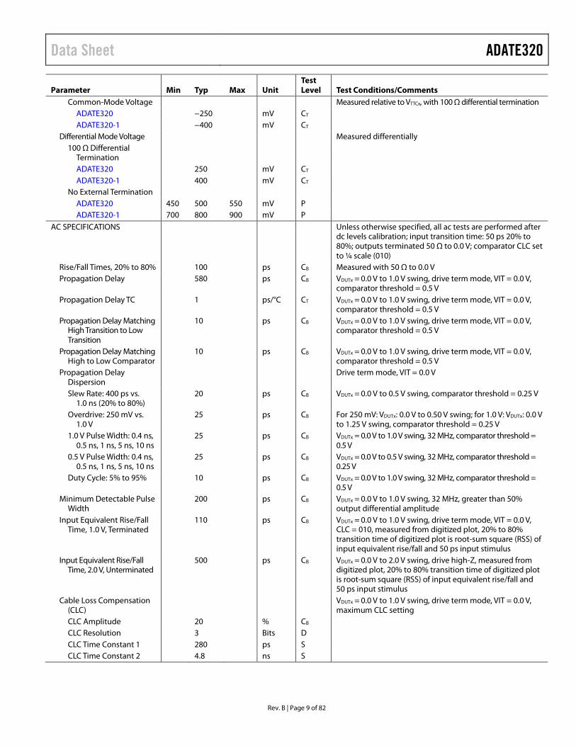
Rev. B | Page 9 of 82
Parameter Min Typ Max Unit Test Level Test Conditions/Comments
Common-Mode Voltage Measured relative to VTTCx, with 100 Ω differential termination ADATE320 −250 mV CT ADATE320-1 −400 mV CT
Differential Mode Voltage Measured differentially 100 Ω Differential
Termination
ADATE320 250 mV CT ADATE320-1 400 mV CT
No External Termination ADATE320 450 500 550 mV P ADATE320-1 700 800 900 mV P
AC SPECIFICATIONS Unless otherwise specified, all ac tests are performed after dc levels calibration; input transition time: 50 ps 20% to 80%; outputs terminated 50 Ω to 0.0 V; comparator CLC set to ¼ scale (010)
Rise/Fall Times, 20% to 80% 100 ps CB Measured with 50 Ω to 0.0 V Propagation Delay 580 ps CB VDUTx = 0.0 V to 1.0 V swing, drive term mode, VIT = 0.0 V,
comparator threshold = 0.5 V Propagation Delay TC 1 ps/°C CT VDUTx = 0.0 V to 1.0 V swing, drive term mode, VIT = 0.0 V,
comparator threshold = 0.5 V Propagation Delay Matching
High Transition to Low Transition
10 ps CB VDUTx = 0.0 V to 1.0 V swing, drive term mode, VIT = 0.0 V, comparator threshold = 0.5 V
Propagation Delay Matching High to Low Comparator
10 ps CB VDUTx = 0.0 V to 1.0 V swing, drive term mode, VIT = 0.0 V, comparator threshold = 0.5 V
Propagation Delay Dispersion
Drive term mode, VIT = 0.0 V
Slew Rate: 400 ps vs. 1.0 ns (20% to 80%)
20 ps CB VDUTx = 0.0 V to 0.5 V swing, comparator threshold = 0.25 V
Overdrive: 250 mV vs. 1.0 V
25 ps CB For 250 mV: VDUTx: 0.0 V to 0.50 V swing; for 1.0 V: VDUTx: 0.0 V to 1.25 V swing, comparator threshold = 0.25 V
1.0 V Pulse Width: 0.4 ns, 0.5 ns, 1 ns, 5 ns, 10 ns
25 ps CB VDUTx = 0.0 V to 1.0 V swing, 32 MHz, comparator threshold = 0.5 V
0.5 V Pulse Width: 0.4 ns, 0.5 ns, 1 ns, 5 ns, 10 ns
25 ps CB VDUTx = 0.0 V to 0.5 V swing, 32 MHz, comparator threshold = 0.25 V
Duty Cycle: 5% to 95% 10 ps CB VDUTx = 0.0 V to 1.0 V swing, 32 MHz, comparator threshold = 0.5 V
Minimum Detectable Pulse Width
200 ps CB VDUTx = 0.0 V to 1.0 V swing, 32 MHz, greater than 50% output differential amplitude
Input Equivalent Rise/Fall Time, 1.0 V, Terminated
110 ps CB VDUTx = 0.0 V to 1.0 V swing, drive term mode, VIT = 0.0 V, CLC = 010, measured from digitized plot, 20% to 80% transition time of digitized plot is root-sum square (RSS) of input equivalent rise/fall and 50 ps input stimulus
Input Equivalent Rise/Fall Time, 2.0 V, Unterminated
500 ps CB VDUTx = 0.0 V to 2.0 V swing, drive high-Z, measured from digitized plot, 20% to 80% transition time of digitized plot is root-sum square (RSS) of input equivalent rise/fall and 50 ps input stimulus
Cable Loss Compensation (CLC)
VDUTx = 0.0 V to 1.0 V swing, drive term mode, VIT = 0.0 V, maximum CLC setting
CLC Amplitude 20 % CB CLC Resolution 3 Bits D CLC Time Constant 1 280 ps S CLC Time Constant 2 4.8 ns S
ADATE320 Data Sheet
Rev. B | Page 10 of 82
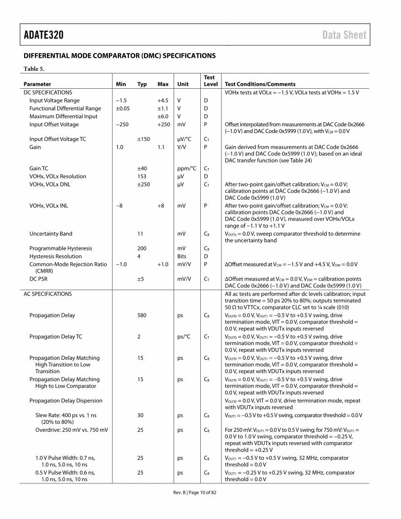
DIFFERENTIAL MODE COMPARATOR (DMC) SPECIFICATIONS
Table 5.
Parameter Min Typ Max Unit Test Level Test Conditions/Comments
DC SPECIFICATIONS VOHx tests at VOLx = −1.5 V, VOLx tests at VOHx = 1.5 V Input Voltage Range −1.5 +4.5 V D Functional Differential Range ±0.05 ±1.1 V D Maximum Differential Input ±6.0 V D Input Offset Voltage −250 +250 mV P Offset interpolated from measurements at DAC Code 0x2666
(−1.0 V) and DAC Code 0x5999 (1.0 V), with VCM = 0.0 V Input Offset Voltage TC ±150 µV/°C CT Gain 1.0 1.1 V/V P Gain derived from measurements at DAC Code 0x2666
(−1.0 V) and DAC Code 0x5999 (1.0 V); based on an ideal DAC transfer function (see Table 24)
Gain TC ±40 ppm/°C CT VOHx, VOLx Resolution 153 µV D VOHx, VOLx DNL ±250 µV CT After two-point gain/offset calibration; VCM = 0.0 V;
calibration points at DAC Code 0x2666 (−1.0 V) and DAC Code 0x5999 (1.0 V)
VOHx, VOLx INL −8 +8 mV P After two-point gain/offset calibration; VCM = 0.0 V; calibration points DAC Code 0x2666 (−1.0 V) and DAC Code 0x5999 (1.0 V), measured over VOHx/VOLx range of −1.1 V to +1.1 V
Uncertainty Band 11 mV CB VDUTx = 0.0 V, sweep comparator threshold to determine the uncertainty band
Programmable Hysteresis 200 mV CB Hysteresis Resolution 4 Bits D Common-Mode Rejection Ratio
(CMRR) −1.0 +1.0 mV/V P ∆Offset measured at VCM = −1.5 V and +4.5 V, VDM = 0.0 V
DC PSR ±5 mV/V CT ∆Offset measured at VCM = 0.0 V, VDM = calibration points DAC Code 0x2666 (−1.0 V) and DAC Code 0x5999 (1.0 V)
AC SPECIFICATIONS All ac tests are performed after dc levels calibration; input transition time = 50 ps 20% to 80%; outputs terminated 50 Ω to VTTCx, comparator CLC set to ¼ scale (010)
Propagation Delay 580 ps CB VDUT0 = 0.0 V, VDUT1 = −0.5 V to +0.5 V swing, drive termination mode, VIT = 0.0 V, comparator threshold = 0.0 V, repeat with VDUTx inputs reversed
Propagation Delay TC 2 ps/°C CT VDUT0 = 0.0 V, VDUT1 = −0.5 V to +0.5 V swing, drive termination mode, VIT = 0.0 V, comparator threshold = 0.0 V, repeat with VDUTx inputs reversed
Propagation Delay Matching High Transition to Low Transition
15 ps CB VDUT0 = 0.0 V, VDUT1 = −0.5 V to +0.5 V swing, drive termination mode, VIT = 0.0 V, comparator threshold = 0.0 V, repeat with VDUTx inputs reversed
Propagation Delay Matching High to Low Comparator
15 ps CB VDUT0 = 0.0 V, VDUT1 = −0.5 V to +0.5 V swing, drive termination mode, VIT = 0.0 V, comparator threshold = 0.0 V, repeat with VDUTx inputs reversed
Propagation Delay Dispersion VDUT0 = 0.0 V, VIT = 0.0 V, drive termination mode, repeat with VDUTx inputs reversed
Slew Rate: 400 ps vs. 1 ns (20% to 80%)
30 ps CB VDUT1 = −0.5 V to +0.5 V swing, comparator threshold = 0.0 V
Overdrive: 250 mV vs. 750 mV 25 ps CB For 250 mV: VDUT1 = 0.0 V to 0.5 V swing; for 750 mV: VDUT1 = 0.0 V to 1.0 V swing, comparator threshold = −0.25 V, repeat with VDUTx inputs reversed with comparator threshold = +0.25 V
1.0 V Pulse Width: 0.7 ns, 1.0 ns, 5.0 ns, 10 ns
25 ps CB VDUT1 = −0.5 V to +0.5 V swing, 32 MHz, comparator threshold = 0.0 V
0.5 V Pulse Width: 0.6 ns, 1.0 ns, 5.0 ns, 10 ns
25 ps CB VDUT1 = −0.25 V to +0.25 V swing, 32 MHz, comparator threshold = 0.0 V

Data Sheet ADATE320
Rev. B | Page 11 of 82
Parameter Min Typ Max Unit Test Level Test Conditions/Comments
Duty Cycle: 5% to 95% 5 ps CB VDUT1 = −0.5 V to +0.5 V swing, 32 MHz, comparator threshold = 0.0 V
Minimum Detectable Pulse Width
200 ps CB VDUT0 = 0.0 V, VDUT1 = −0.5 V to +0.5 V swing, 32 MHz, drive term mode, VIT = 0.0 V, comparator threshold = 0.0 V, greater than 50% output differential amplitude, repeat with VDUTx inputs reversed
Input Equivalent Rise/Fall Time 110 ps CB VDUT0 = 0.0 V, VDUT1 = −0.5 V to +0.5 V swing, drive term mode, VIT = 0.0 V, comparator threshold = 0.0 V, CLC = ¼ scale, measured from digitized plot, t = √(tCMP
2 − tIN2)
Cable Loss Compensation (CLC) VDUT0 = 0.0 V, VDUT1 = −0.8 V to +0.8 V swing, drive term mode, VIT = 0.0 V, comparator threshold = 0.0 V, comparator CLC set to maximum CLC setting, repeat with VDUTx inputs reversed
CLC Amplitude 20 % CB CLC Resolution 3 Bits D CLC Time Constant 1 280 ps S CLC Time Constant 2 4.8 ns S
ACTIVE LOAD SPECIFICATIONS
Table 6.
Parameter Min Typ Max Unit Test Level Test Conditions/Comments
DC SPECIFICATIONS Load in active on state, RCVx active Input Characteristics
Active Load Commutation Voltage (VCOMx) Range
−1.5 +4.5 V D IOHx = IOLx = 1 mA, VDUTx open circuit
VCOMx Offset −200 +200 mV P Measured at DAC Code 0x4000 (0.0 V), uncalibrated VCOMx Offset TC ±100 µV/°C CT VCOMx Gain 1.0 1.1 V/V P Gain derived from measurements at DAC Code 0x4000
(0.0 V) and DAC Code 0x8CCC (3.0 V) VCOMx Gain TC ±20 ppm/°C CT VCOMx Resolution 153 µV D VCOMx DNL ±250 µV CT IOHx = IOLx = 12.5 mA, after two-point gain/offset
calibration; measured over VCOMx range −1.5 V to +4.5 V; calibration points DAC Code 0x4000 (0.0 V) and DAC Code 0x8CCC (3.0 V)
VCOMx INL IOHx = IOLx = 12.5 mA; after two-point gain/offset calibration; calibration points DAC Code 0x4000 (0.0 V) and DAC Code 0x8CCC (3.0 V)
Focused Range −5 +5 mV P Measured over VCOMx range of −0.5 V to +3.5 V Full Range −10 +10 mV P Measured over VCOMx range of −1.5 V to +4.5 V
DUTGND Voltage Accuracy −5 ±1 +5 mV P Over ±0.1 V range; measured over −0.5 V to +3.5 V focused VCOMx range
Output Characteristics Maximum Source Current
(IOLx) 25 mA D VDUTx ≤ 3.5 V (a compliance limit is set by a 50 Ω
internal resistor as illustrated in Figure 142) IOLx Offset −600 +600 µA P IOHx = −2.5 mA, VCOMx = 1.5 V, VDUTx = 0.0 V; offset
extrapolated from measurements at DAC Code 0x451F (1 mA) and DAC Code 0xA666 (20 mA)
IOLx Offset TC ±1 µA/°C CT IOLx Gain Error 0 +25 % P IOHx = −2.5 mA, VCOMx = 1.5 V, VDUTx = 0.0 V; gain
derived from measurements at DAC Code 0x451F (1 mA) and DAC Code 0xA666 (20 mA); based on an ideal dc transfer function
IOLx Gain TC ±100 ppm/°C CT

ADATE320 Data Sheet
Rev. B | Page 12 of 82
Parameter Min Typ Max Unit Test Level Test Conditions/Comments
IOLx Resolution 763 nA D IOLx DNL ±1.25 µA CT IOHx = −2.5 mA, VCOMx = 1.5 V, VDUTx = 0.0 V; after
two-point gain/offset calibration; measured over IOLx range 0 mA to 25 mA; calibrated at DAC Code 0x451F (1 mA) and DAC Code 0xA666 (20 mA)
IOLx INL −100 +100 µA P IOHx = −2.5 mA, VCOM = 1.5 V, VDUTx = 0.0 V, after two-point gain/offset calibration
IOLx 90% Commutation Voltage
0.25 0.4 V P IOHx = IOLx = 25 mA, VCOM = 2.0 V, measure IOLx reference at VDUTx = −1.0 V, measure IOLx current at VDUTx = 1.6 V, check > 90% of reference current
0.1 V CT IOHx = IOLx = 1 mA, VCOM = 2.0 V, measure IOLx reference at VDUTx = −1.0 V, measure IOLx current at VDUTx = 1.9 V, check > 90% of reference current
Maximum Sink Current (IOHx) 25 mA D VDUTx ≥ −0.5 V (a compliance limit is set by a 50 Ω internal resistor as illustrated in Figure 142)
IOHx Offset −600 +600 µA P IOLx = −2.5 mA, VCOM = 1.5 V, VDUTx = 3.0 V, offset extrapolated from measurements at DAC Code 0x451F (1 mA) and DAC Code 0xA666 (20 mA)
IOHx Offset TC ±1 µA/°C CT IOHx Gain Error 0 +25 % P IOLx = −2.5 mA, VCOM = 1.5 V, VDUTx = 3.0 V, gain
derived from measurements at DAC Code 0x451F (1 mA) and DAC Code 0xA666 (20 mA); based on an ideal DAC transfer function
IOHx Gain TC ±100 ppm/°C CT IOHx Resolution 763 nA D IOHx DNL ±1.25 µA CT IOLx = −2.5 mA, VCOM = 1.5 V, VDUTx = 3.0 V, after
two-point gain/offset calibration; measured over IOHx range of 0 mA to 25 mA; calibrated at DAC Code 0x451F (1 mA) and DAC Code 0xA666 (20 mA)
IOHx INL −100 +100 µA P IOLx = −2.5 mA, VCOM = 1.5 V, VDUTx = 3.0 V, after two-point gain/offset calibration
IOHx 90% Commutation Voltage
0.25 0.4 V P IOHx = IOLx = 25 mA, VCOM = 2.0 V, measure IOHx reference at VDUTx = 4.0 V, measure IOHx current at VDUTx = 2.4 V, ensure > 90% of reference current
0.1 V CT IOHx = IOLx = 1 mA, VCOM = 2.0 V, measure IOHx reference at VDUTx = 4.0 V, measure IOHx current at VDUTx = 2.1 VDUTx, ensure > 90% of reference current
AC SPECIFICATIONS All ac measurements are performed after dc calibration unless noted, load active on
Dynamic Performance Toggle RCVx; DUTx terminated 50 Ω to 0.0 V; IOLx = IOHx = 20 mA, VIH = VIL = 0.0 V; VCOM = +1.5 V for IOLx and −1.5 V for IOHx
Propagation Delay, Load Active On to Load Active Off
1.7 ns CB Measured from zero crossing of RCVx − RCVx to 50% of final output value; repeat for drive low and drive high
Propagation Delay, Load Active Off to Load Active On
2.9 ns CB Measured from zero crossing of RCVx − RCVx to 50% of final output value; repeat for drive low and drive high
Propagation Delay Matching 1.2 ns CB Active on vs. active off; repeat for drive low and drive high
Load Spike 140 mV CB Repeat for drive low and drive high Settling Time to Within 5% 2.5 ns CB Measured from output crossing 50% final value to
output within 5% final value

Data Sheet ADATE320
Rev. B | Page 13 of 82
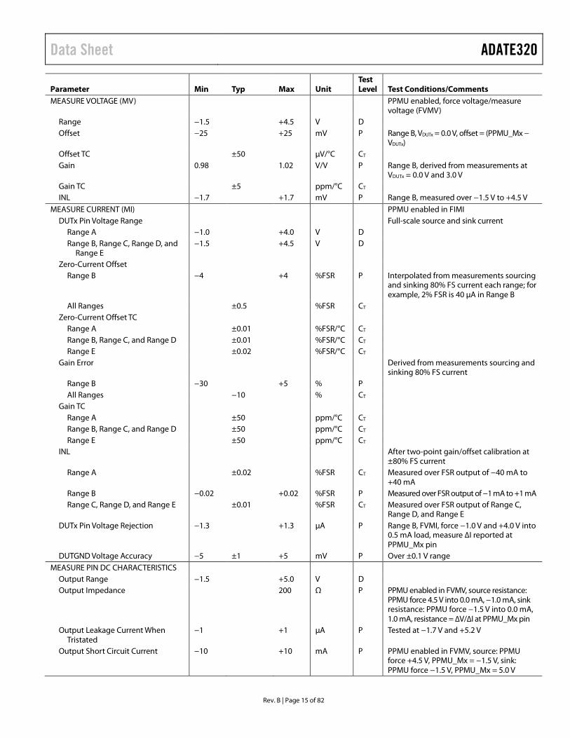
PPMU SPECIFICATIONS PPMU enabled in force voltage mode unless noted.
Table 7.
Parameter Min Typ Max Unit Test Level Test Conditions/Comments
FORCE VOLTAGE (FV) Current Range A −40 +40 mA D Current Range B −1 +1 mA D Current Range C −100 +100 µA D Current Range D −10 +10 µA D Current Range E −2 +2 µA D FV Range at Output, Range A −1.0 +4.0 V D Output range for full-scale source/sink −1.5 +4.5 V D Output range for ±25 mA or less FV Range at Output, Range B,
Range C, Range D, and Range E −1.5 +4.5 V D Output range for full-scale source/sink
FV Offset, Range C −100 +100 mV P Measured at DAC Code 0x4000 (0.0 V) in Range C
FV Offset, All Ranges ±30 mV CT Measured at DAC Code 0x4000 (0.0 V) applies to all other ranges
FV Offset TC, All Ranges ±100 µV/°C CT Measured at DAC Code 0x4000 (0.0 V) FV Gain, Range C 1.0 1.1 V/V P Gain derived from measurements at DAC
Code 0x4000 (0.0 V) and DAC Code 0x8CCC (3.0 V); based on an ideal DAC transfer function
FV Gain, All Ranges 1.05 V/V CT Gain derived from measurements at DAC Code 0x4000 (0.0 V) and DAC Code 0x8CCC (3.0 V); based on an ideal DAC transfer function
FV Gain TC, All Ranges ±10 ppm/°C CT Gain derived from measurements at DAC Code 0x4000 (0.0 V) and DAC Code 0x8CCC (3.0 V)
FV INL Range A ±1.5 mV CT After two-point gain/offset calibration,
output range of −1.5 V to +4.5 V; calibration points DAC Code 0x4000 (0.0 V) and DAC Code 0x8CCC (3.0 V), PPMU Current Range A
Range C, Focused Range −1.7 +1.7 mV P After two-point gain/offset calibration, output range of −0.5 V to +3.5 V; calibration points DAC Code 0x4000 (0.0 V) and DAC Code 0x8CCC (3.0 V)
Range C, Full Range −5 +5 mV P After two-point gain/offset calibration, output range of −1.5 V to +4.5 V; calibration points DAC Code 0x4000 (0.0 V) and DAC Code 0x8CCC (3.0 V)
Range B, Range D, and Range E ±1.0 mV CT After two-point gain/offset calibration, output range of −1.5 V to +4.5 V; calibration points DAC Code 0x4000 (0.0 V) and DAC Code 0x8CCC (3.0 V)
FV Compliance vs. Source/Sink Current, Range A (±40 mA)
±1 mV CT Force −1.0 V; measure voltage while sinking 0.0 mA and full-scale current; measure ∆V; force 4.0 V; measure voltage while sourcing 0.0 mA and full-scale current; measure ∆V
FV Compliance vs. Source/Sink Current, Range A (±25 mA)
±1 mV CT Force −1.5 V; measure voltage while sinking 0.0 mA and 25 mA; measure ∆V; force 4.5 V; measure voltage while sourcing 0.0 mA and 25 mA; measure ∆V

ADATE320 Data Sheet
Rev. B | Page 14 of 82
Parameter Min Typ Max Unit Test Level Test Conditions/Comments
FV Compliance vs. Source/Sink Current, Range B, Range C, Range D, and Range E
±1 mV CT Force −1.5 V; measure voltage while sinking 0.0 mA and full-scale current; measure ∆V; force 4.5 V; measure voltage while sourcing 0.0 mA and full-scale current; measure ∆V
DUTGND Voltage Accuracy −5 ±1 +5 mV P Over ±0.1 V range; measured over −0.5 V to +3.5 V focused PPMU output range
FORCE CURRENT (FI) PPMU enabled in force current/measure current (FIMI)
DUTx Pin Voltage Range, Range A −1.0 +4.0 V D Full-scale source and sink current −1.5 +4.5 V D DUTx pin source and sink 25 mA or less DUTx Pin Voltage Range, Range B,
Range C, Range D, and Range E −1.5 +4.5 V D Full-scale source and sink current
Zero-Current Offset, All Ranges −14.5 +14.5 % FSR P Interpolated from measurements at PPMU DAC Code 0x4CCC (−80% FS) and DAC Code 0xB333 (80% FS) for each range
Zero-Current Offset TC ±0.02 % FSR/°C CT Gain Error, All Ranges 0 30 % P Derived from measurements at PPMU DAC
Code 0x4CCC (−80% FS) and DAC Code 0xB333 (80% FS) for each range
Gain Drift Range A ±50 ppm/°C CT PPMU self heating effects in Range A can
influence gain drift measurements Range B ±50 ppm/°C CT Range C, Range D, and Range E ±50 ppm/°C CT
INL After two-point gain/offset calibration Range A −0.12 +0.12 % FSR P Measured over FSR output of Range A
(±40 mA) Range B, Range C, and Range D −0.04 +0.04 % FSR P Measured over FSR output of Range B
(±1 mA), Range C (±100 µA), and Range D (±10 µA)
Range E −0.045 +0.045 % FSR P Measured over FSR output of Range E (±2 µA)
FI Compliance vs. Voltage Load Range A −0.3 +0.3 % FSR P Force positive full-scale current driving
−1.0 V and +4.0 V, measure ∆I at DUTx pin; force negative full-scale current driving −1.0 V and +4.0 V, measure ∆I at DUTx pin
−0.1 +0.1 % FSR P Force positive full-scale current driving 0.0 V and 3.0 V, measure ∆I at DUTx pin; force negative full-scale current driving 0.0 V and 3.0 V, measure ∆I at DUTx pin
Range B and Range C −0.3 +0.3 % FSR P Force positive full-scale current driving −1.5 V and +4.5 V, measure ∆I at DUTx pin; force negative full-scale current driving −1.5 V and +4.5 V, measure ∆I at DUTx pin
−0.06 +0.06 % FSR P Force positive full-scale current driving 0.0 V and 3.0 V, measure ∆I at DUTx pin; force negative full-scale current driving 0.0 V and 3.0 V, measure ∆I at DUTx pin
Range D −0.3 +0.3 % FSR P Force positive full-scale current driving −1.5 V and +4.5 V, measure ∆I at DUTx pin; force negative full-scale current driving −1.5 V and +4.5 V, measure ∆I at DUTx pin
Range E −0.85 +0.85 % FSR P Force positive full-scale current driving −1.5 V and +4.5 V, measure ∆I at DUTx pin; force negative full-scale current driving −1.5 V and +4.5 V, measure ∆I at DUTx pin; allows 10 nA DUTx pin leakage
Data Sheet ADATE320
Rev. B | Page 15 of 82
Parameter Min Typ Max Unit Test Level Test Conditions/Comments
MEASURE VOLTAGE (MV) PPMU enabled, force voltage/measure voltage (FVMV)
Range −1.5 +4.5 V D Offset −25 +25 mV P Range B, VDUTx = 0.0 V, offset = (PPMU_Mx −
VDUTx) Offset TC ±50 µV/°C CT Gain 0.98 1.02 V/V P Range B, derived from measurements at
VDUTx = 0.0 V and 3.0 V Gain TC ±5 ppm/°C CT INL −1.7 +1.7 mV P Range B, measured over −1.5 V to +4.5 V
MEASURE CURRENT (MI) PPMU enabled in FIMI DUTx Pin Voltage Range Full-scale source and sink current
Range A −1.0 +4.0 V D Range B, Range C, Range D, and
Range E −1.5 +4.5 V D
Zero-Current Offset Range B −4 +4 %FSR P Interpolated from measurements sourcing
and sinking 80% FS current each range; for example, 2% FSR is 40 µA in Range B
All Ranges ±0.5 %FSR CT Zero-Current Offset TC
Range A ±0.01 %FSR/°C CT Range B, Range C, and Range D ±0.01 %FSR/°C CT Range E ±0.02 %FSR/°C CT
Gain Error Derived from measurements sourcing and sinking 80% FS current
Range B −30 +5 % P All Ranges −10 % CT
Gain TC Range A ±50 ppm/°C CT Range B, Range C, and Range D ±50 ppm/°C CT Range E ±50 ppm/°C CT
INL After two-point gain/offset calibration at ±80% FS current
Range A ±0.02 %FSR CT Measured over FSR output of −40 mA to +40 mA
Range B −0.02 +0.02 %FSR P Measured over FSR output of −1 mA to +1 mA Range C, Range D, and Range E ±0.01 %FSR CT Measured over FSR output of Range C,
Range D, and Range E DUTx Pin Voltage Rejection −1.3 +1.3 µA P Range B, FVMI, force −1.0 V and +4.0 V into
0.5 mA load, measure ∆I reported at PPMU_Mx pin
DUTGND Voltage Accuracy −5 ±1 +5 mV P Over ±0.1 V range MEASURE PIN DC CHARACTERISTICS
Output Range −1.5 +5.0 V D Output Impedance 200 Ω P PPMU enabled in FVMV, source resistance:
PPMU force 4.5 V into 0.0 mA, −1.0 mA, sink resistance: PPMU force −1.5 V into 0.0 mA, 1.0 mA, resistance = ∆V/∆I at PPMU_Mx pin
Output Leakage Current When Tristated
−1 +1 µA P Tested at −1.7 V and +5.2 V
Output Short Circuit Current −10 +10 mA P PPMU enabled in FVMV, source: PPMU force +4.5 V, PPMU_Mx = −1.5 V, sink: PPMU force −1.5 V, PPMU_Mx = 5.0 V

ADATE320 Data Sheet
Rev. B | Page 16 of 82
Parameter Min Typ Max Unit Test Level Test Conditions/Comments
PPMU_Mx Pin, Parasitic Output Capacitance
2 pF S Parasitic capacitance contributed by pin
PPMU_Mx Pin, External Load Capacitance
100 pF S External capacitance tolerated by pin (exceeding this value may cause instability)
PPMU VOLTAGE CLAMPS (FI) PPMU enabled in FIMI, PPMU clamps enabled; clamp accuracy applies only when |PCHx − PCLx| ≥ 1.0 V
Low Voltage Clamp Range (PCLx) −1.5 +3.5 V D High Voltage Clamp Range (PCHx) −0.5 +4.5 V D Offset, Voltage Clamps (PCHx/PCLx) −300 +300 mV P Range B, PPMU force ±0.5 mA into open;
PCHx measured at DAC Code 0x4000 (0.0 V) with PCLx at DAC Code 0x0000 (−2.5 V); PCLx measured at DAC Code 0x4000 (0.0 V) with PCHx at DAC Code 0xFFFF (+7.5 V)
Offset TC, Voltage Clamps (PCHx/PCLx) ±0.5 mV/°C CT Gain, Voltage Clamps (PCHx/PCLx) 1.0 1.1 V/V P Range B, PPMU force ±0.5 mA into open; PCHx
gain derived from measurements at DAC Code 0x4000 (0.0 V) and DAC Code 0x8CCC (3.0 V) with PCLx at DAC Code 0x0000 (−2.5 V); PCLx gain derived from measure-ments at DAC Code 0x4000 (0.0 V) and DAC Code 0x8CCC (3.0 V) with PCHx at DAC Code 0xFFFF (7.5 V)
Gain TC, Voltage Clamps (PCHx/PCLx) ±25 ppm/°C CT INL, Voltage Clamps (PCHx/PCLx) −20 +20 mV P Range B, PPMU force ±0.5 mA into open
after two-point gain/offset calibration; measured over PPMU clamp functional range
Positive Voltage Clamp, Voltage Droop (Source)
−50 +50 mV P ∆V at DUTx pin, Range A, PCHx = +4.0 V, PCLx = −1.0 V, PPMU force 5.0 mA and 40 mA into open circuit, calibrated
Negative Voltage Clamp, Voltage Droop (Sink)
−50 +50 mV P ∆V at DUTx pin, Range A, PCHx = +4.0 V, PCLx = −1.0 V, PPMU force −5.0 mA and −40 mA into open circuit, calibrated
DUTGND Voltage Accuracy −5 ±1 +5 mV P Over ±0.1 V range; measured at end points of clamp functional range
PPMU CURRENT CLAMPS (FV) PPMU enabled in FVMV, dc accuracy of the current clamps only applies over the following conditions: 30% FS ≤ PCHx ≤ 100% FS or −100% FS ≤ PCLx ≤ −30% FS
Functional Range Low Current Clamp (PCLx) −120 −20 %FS S For example, −120% FS in Range A is
−48 mA and −20% FS in Range A is −8 mA High Current Clamp (PCHx) 20 120 %FS S For example, 20% FS in Range A is 8 mA
and 120% FS in Range A is 48 mA DC Accuracy Range
Low Current Clamp (PCLx) −100 −30 %FS D For example, −100% FS in Range A is −40 mA and −30% FS in Range A is −12 mA
High Current Clamp (PCHx) 30 100 %FS D For example, 30% FS in Range A is 12 mA and 100% FS in Range A is 40 mA
Static Current Limit, Source and Sink, All Ranges
±120 ±140 ±160 %FS P PCLx at DAC Code 0x0000 (−2.5 V), PCHx at DAC Code 0xFFFF (7.5 V), sink: force −1.5 V, short DUTx to 4.5 V, source: force 4.5 V, short DUTX to −1.5 V
Offset, Current Clamps (PCHx/PCLx) −10 +10 %FSR P All ranges; PPMU force ±1.0 V into 0.0 V1 Offset TC, Current Clamps
(PCHx/PCLx) ±0.02 %FSR/°C CT All ranges

Data Sheet ADATE320
Rev. B | Page 17 of 82
Parameter Min Typ Max Unit Test Level Test Conditions/Comments
Gain Error, Current Clamps (PCHx/PCLx)
0 30 % P All ranges; PPMU force ±1.0 V into 0.0 V2
Gain TC, Current Clamps (PCHx/PCLx)
±50 ppm/°C CT All ranges
INL, Current Clamps (PCHx/PCLx) −0.15 +0.15 %FSR P All ranges; PPMU force ±1.0 V into 0.0 V, after two-point gain/offset calibration; PCHx calibration at DAC Code 0xA000 (3.75 V or 50% FS) and DAC Code 0xB333 (4.50 V or 80% FS); PCLx calibration at DAC Code 0x6000 (1.25 V or −50% FS) and DAC Code 0x4CCC (0.50 V or −80% FS); measured over dc accuracy range
Current Droop Low Current Clamp (PCLx), Sink −2 +2 %FSR P PCLx = 0.5 V (−80% FS), PCHx = 4.5 V (80%
FS), PPMU force −0.5 V and +3.5 V into VDUTx = 4.5 V, measure ∆I at the DUTx pin in Range A
High Current Clamp (PCHx), Source
−2 +2 %FSR P PCLx = 0.5 V (−80% FS), PCHx = 4.5 V (80% FS), PPMU force −0.5 V and +3.5 V into VDUTx = −1.5 V, measure ∆I at the DUTx pin in Range A
SETTLING/SWITCHING TIMES FV Settling Time to 0.1% of Final
Value
Range A, 200 pF and 2000 pF Load
20 µs S PPMU enabled in FV, Range A, step from 0.0 V to 4.0 V
Range B, 200 pF and 2000 pF Load
25 µs S PPMU enabled in FV, Range B, DCL disabled, step from 0.0 V to 4.0 V
Range C, 200 pF Load 25 µs S PPMU enabled in FV, Range C, DCL disabled, step from 0.0 V to 4.0 V
Range C, 2000 pF Load 65 µs S PPMU enabled in FV, Range C, DCL disabled, step from 0.0 V to 4.0 V
FV Settling Time to 1.0% of Final Value
Range A, 200 pF and 2000 pF Load 16 µs CB PPMU enabled in FV, Range A, DCL disabled, step from 0.0 V to 4.0 V
Range B, 200 pF and 2000 pF Load 14 µs CB PPMU enabled in FV, Range B, DCL disabled, step from 0.0 V to 4.0 V
Range C, 200 pF and 2000 pF Load 18 µs CB PPMU enabled in FV, Range C, DCL disabled enabled, step from 0.0 V to 4.0 V
FI Settling Time to 0.1% of Final Value
Range A, 200 pF in Parallel with 120 Ω
16 µs S PPMU enabled in FI, Range A, DCL disabled, step from 0.0 mA to 40 mA
Range B, 200 pF in Parallel with 1.5 kΩ
10 µs S PPMU enabled in FI, Range B, DCL disabled, step from 0.0 mA to 1 mA
Range C, 200 pF in Parallel with 15.0 kΩ
40 µs S PPMU enabled in FI, Range C, DCL disabled, step from 0.0 mA to 100 µA
FI Settling Time to 1.0% of Final Value
Range A, 200 pF in Parallel with 120 Ω
8 µs CB PPMU enabled in FI, Range A, DCL disabled, step from 0.0 mA to 40 mA
Range B, 200 pF in Parallel with 1.5 kΩ
8 µs CB PPMU enabled in FI, Range B, DCL disabled, step from 0.0 mA to 1 mA
Range C, 200 pF in Parallel with 15.0 kΩ
8 µs CB PMU enabled in FI, Range C, DCL disabled, step from 0.0 mA to 100 µA
ADATE320 Data Sheet
Rev. B | Page 18 of 82
Parameter Min Typ Max Unit Test Level Test Conditions/Comments
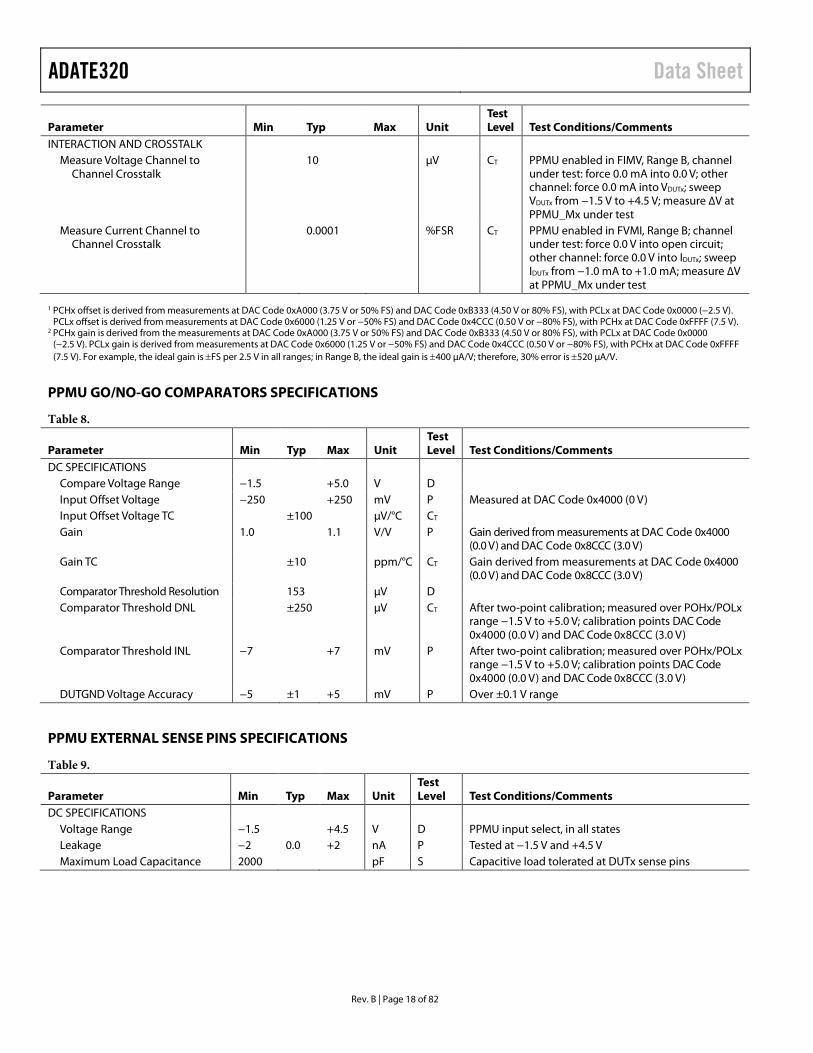
INTERACTION AND CROSSTALK Measure Voltage Channel to
Channel Crosstalk 10 µV CT PPMU enabled in FIMV, Range B, channel
under test: force 0.0 mA into 0.0 V; other channel: force 0.0 mA into VDUTx; sweep VDUTx from −1.5 V to +4.5 V; measure ∆V at PPMU_Mx under test
Measure Current Channel to Channel Crosstalk
0.0001 %FSR CT PPMU enabled in FVMI, Range B; channel under test: force 0.0 V into open circuit; other channel: force 0.0 V into IDUTx; sweep IDUTx from −1.0 mA to +1.0 mA; measure ∆V at PPMU_Mx under test
1 PCHx offset is derived from measurements at DAC Code 0xA000 (3.75 V or 50% FS) and DAC Code 0xB333 (4.50 V or 80% FS), with PCLx at DAC Code 0x0000 (−2.5 V).
PCLx offset is derived from measurements at DAC Code 0x6000 (1.25 V or −50% FS) and DAC Code 0x4CCC (0.50 V or −80% FS), with PCHx at DAC Code 0xFFFF (7.5 V). 2 PCHx gain is derived from the measurements at DAC Code 0xA000 (3.75 V or 50% FS) and DAC Code 0xB333 (4.50 V or 80% FS), with PCLx at DAC Code 0x0000
(−2.5 V). PCLx gain is derived from measurements at DAC Code 0x6000 (1.25 V or −50% FS) and DAC Code 0x4CCC (0.50 V or −80% FS), with PCHx at DAC Code 0xFFFF (7.5 V). For example, the ideal gain is ±FS per 2.5 V in all ranges; in Range B, the ideal gain is ±400 µA/V; therefore, 30% error is ±520 µA/V.
PPMU GO/NO-GO COMPARATORS SPECIFICATIONS
Table 8.
Parameter Min Typ Max Unit Test Level Test Conditions/Comments
DC SPECIFICATIONS Compare Voltage Range −1.5 +5.0 V D Input Offset Voltage −250 +250 mV P Measured at DAC Code 0x4000 (0 V) Input Offset Voltage TC ±100 μV/°C CT Gain 1.0 1.1 V/V P Gain derived from measurements at DAC Code 0x4000
(0.0 V) and DAC Code 0x8CCC (3.0 V) Gain TC ±10 ppm/°C CT Gain derived from measurements at DAC Code 0x4000
(0.0 V) and DAC Code 0x8CCC (3.0 V) Comparator Threshold Resolution 153 µV D Comparator Threshold DNL ±250 µV CT After two-point calibration; measured over POHx/POLx
range −1.5 V to +5.0 V; calibration points DAC Code 0x4000 (0.0 V) and DAC Code 0x8CCC (3.0 V)
Comparator Threshold INL −7 +7 mV P After two-point calibration; measured over POHx/POLx range −1.5 V to +5.0 V; calibration points DAC Code 0x4000 (0.0 V) and DAC Code 0x8CCC (3.0 V)
DUTGND Voltage Accuracy −5 ±1 +5 mV P Over ±0.1 V range
PPMU EXTERNAL SENSE PINS SPECIFICATIONS
Table 9.
Parameter Min Typ Max Unit Test Level Test Conditions/Comments
DC SPECIFICATIONS Voltage Range −1.5 +4.5 V D PPMU input select, in all states Leakage −2 0.0 +2 nA P Tested at −1.5 V and +4.5 V Maximum Load Capacitance 2000 pF S Capacitive load tolerated at DUTx sense pins
Data Sheet ADATE320
Rev. B | Page 19 of 82
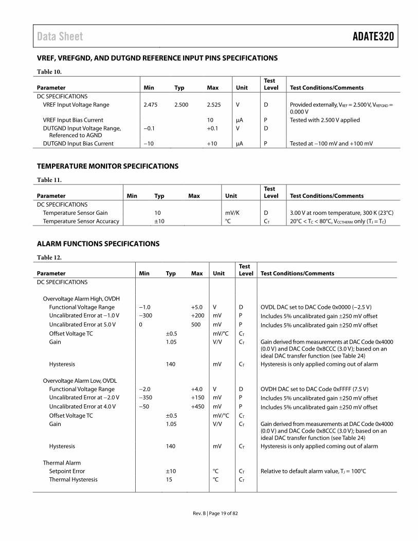
VREF, VREFGND, AND DUTGND REFERENCE INPUT PINS SPECIFICATIONS
Table 10.
Parameter Min Typ Max Unit Test Level Test Conditions/Comments
DC SPECIFICATIONS VREF Input Voltage Range 2.475 2.500 2.525 V D Provided externally, VREF = 2.500 V, VREFGND =
0.000 V VREF Input Bias Current 10 µA P Tested with 2.500 V applied DUTGND Input Voltage Range,
Referenced to AGND −0.1 +0.1 V D
DUTGND Input Bias Current −10 +10 µA P Tested at −100 mV and +100 mV
TEMPERATURE MONITOR SPECIFICATIONS
Table 11.
Parameter Min Typ Max Unit Test Level Test Conditions/Comments
DC SPECIFICATIONS Temperature Sensor Gain 10 mV/K D 3.00 V at room temperature, 300 K (23°C) Temperature Sensor Accuracy ±10 °C CT 20°C < TC < 80°C, VCCTHERM only (TJ = TC)
ALARM FUNCTIONS SPECIFICATIONS
Table 12.
Parameter Min Typ Max Unit Test Level Test Conditions/Comments
DC SPECIFICATIONS Overvoltage Alarm High, OVDH
Functional Voltage Range −1.0 +5.0 V D OVDL DAC set to DAC Code 0x0000 (−2.5 V) Uncalibrated Error at −1.0 V −300 +200 mV P Includes 5% uncalibrated gain ±250 mV offset Uncalibrated Error at 5.0 V 0 500 mV P Includes 5% uncalibrated gain ±250 mV offset Offset Voltage TC ±0.5 mV/°C CT Gain 1.05 V/V CT Gain derived from measurements at DAC Code 0x4000
(0.0 V) and DAC Code 0x8CCC (3.0 V); based on an ideal DAC transfer function (see Table 24)
Hysteresis 140 mV CT Hysteresis is only applied coming out of alarm Overvoltage Alarm Low, OVDL
Functional Voltage Range −2.0 +4.0 V D OVDH DAC set to DAC Code 0xFFFF (7.5 V) Uncalibrated Error at −2.0 V −350 +150 mV P Includes 5% uncalibrated gain ±250 mV offset Uncalibrated Error at 4.0 V −50 +450 mV P Includes 5% uncalibrated gain ±250 mV offset Offset Voltage TC ±0.5 mV/°C CT Gain 1.05 V/V CT Gain derived from measurements at DAC Code 0x4000
(0.0 V) and DAC Code 0x8CCC (3.0 V); based on an ideal DAC transfer function (see Table 24)
Hysteresis 140 mV CT Hysteresis is only applied coming out of alarm Thermal Alarm
Setpoint Error ±10 °C CT Relative to default alarm value, TJ = 100°C Thermal Hysteresis 15 °C CT
ADATE320 Data Sheet
Rev. B | Page 20 of 82
Parameter Min Typ Max Unit Test Level Test Conditions/Comments
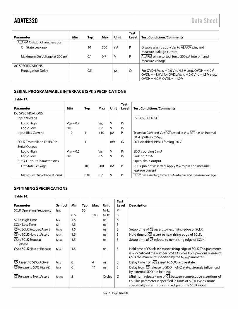
ALARM Output Characteristics
Off State Leakage 10 500 nA P Disable alarm, apply VDD to ALARM pin, and measure leakage current
Maximum On Voltage at 200 µA 0.1 0.7 V P ALARM pin asserted, force 200 µA into pin and measure voltage
AC SPECIFICATIONS Propagation Delay 0.5 µs CB For OVDH: VDUTx = 0.0 V to 4.5 V step, OVDH = 4.0 V,
OVDL = −1.0 V; for OVDL: VDUTx = 0.0 V to −1.5 V step, OVDH = 4.0 V, OVDL = −1.0 V
SERIAL PROGRAMMABLE INTERFACE (SPI) SPECIFICATIONS
Table 13.
Parameter Min Typ Max Unit Test Level Test Conditions/Comments
DC SPECIFICATIONS Input Voltage RST, CS, SCLK, SDI
Logic High VDD − 0.7 VDD V PF Logic Low 0.0 0.7 V PF
Input Bias Current −10 1 +10 µA P Tested at 0.0 V and VDD; RST tested at VDD; RST has an internal 50 kΩ pull-up to VDD
SCLK Crosstalk on DUTx Pin 1 mV CB DCL disabled, PPMU forcing 0.0 V Serial Output
Logic High VDD − 0.5 VDD V PF SDO, sourcing 2 mA Logic Low 0.0 0.5 V PF Sinking 2 mA
BUSY Output Characteristics Open-drain output
Off State Leakage 10 500 nA P BUSY pin not asserted, apply VDD to pin and measure leakage current
Maximum On Voltage at 2 mA 0.01 0.7 V P BUSY pin asserted, force 2 mA into pin and measure voltage
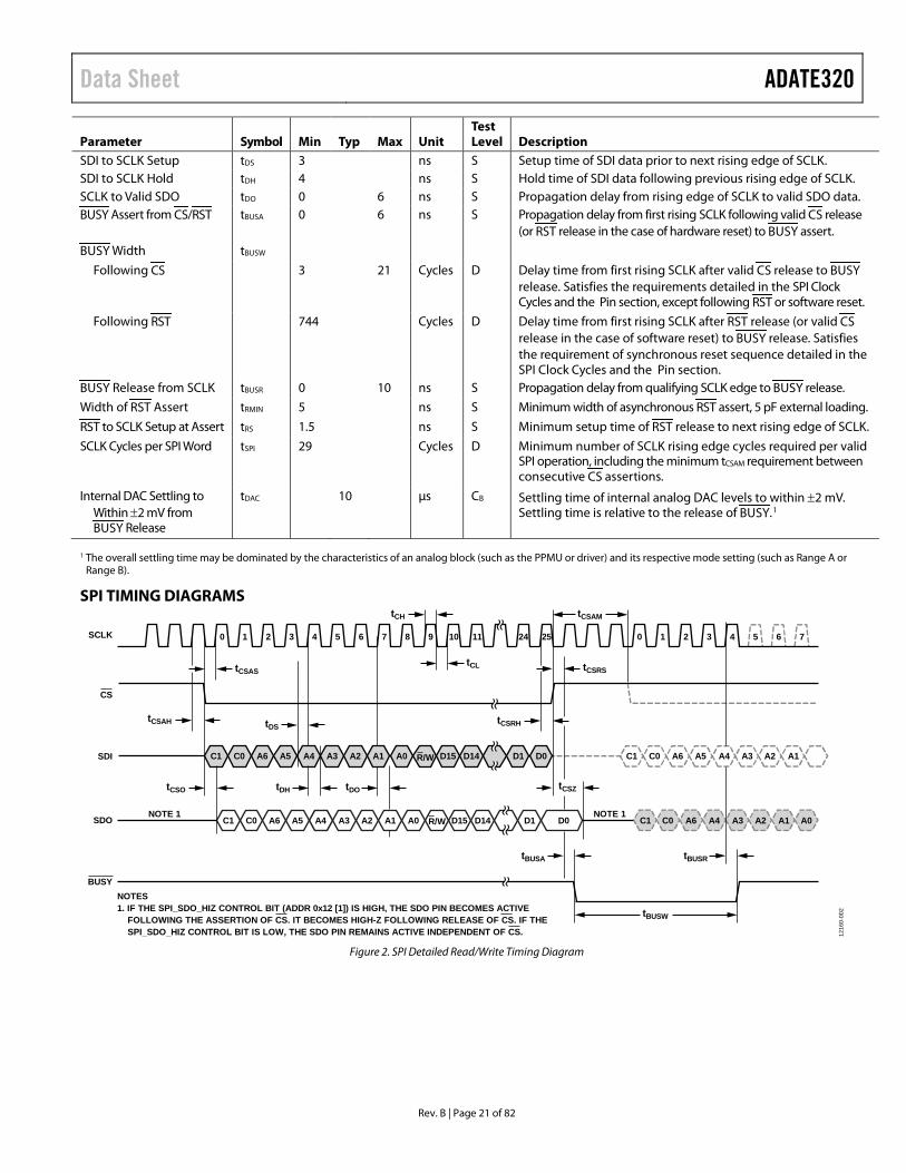
SPI TIMING SPECIFICATIONS
Table 14.
Parameter Symbol Min Typ Max Unit Test Level Description
SCLK Operating Frequency fCLK 50 MHz PF 0.5 100 MHz S SCLK High Time tCH 4.5 ns S SCLK Low Time tCL 4.5 ns S CS to SCLK Setup at Assert tCSAS 1.5 ns S Setup time of CS assert to next rising edge of SCLK.
CS to SCLK Hold at Assert tCSAH 1.5 ns S Hold time of CS assert to next rising edge of SCLK.
CS to SCLK Setup at Release
tCSRS 1.5 ns S Setup time of CS release to next rising edge of SCLK.
CS to SCLK Hold at Release tCSRH 1.5 ns S Hold time of CS release to next rising edge of SCLK. This parameter is only critical if the number of SCLK cycles from previous release of CS is the minimum specified by the tCSAM parameter.
CS Assert to SDO Active tCSO 0 4 ns S Delay time from CS assert to SDO active state.
CS Release to SDO High-Z tCSZ 0 11 ns S Delay from CS release to SDO high-Z state, strongly influenced by external SDO pin loading.
CS Release to Next Assert tCSAM 3 Cycles D Minimum release time of CS between consecutive assertions of CS. This parameter is specified in units of SCLK cycles, more specifically in terms of rising edges of the SCLK input.
Data Sheet ADATE320
Rev. B | Page 21 of 82
Parameter Symbol Min Typ Max Unit Test Level Description
SDI to SCLK Setup tDS 3 ns S Setup time of SDI data prior to next rising edge of SCLK. SDI to SCLK Hold tDH 4 ns S Hold time of SDI data following previous rising edge of SCLK. SCLK to Valid SDO tDO 0 6 ns S Propagation delay from rising edge of SCLK to valid SDO data. BUSY Assert from CS/RST tBUSA 0 6 ns S Propagation delay from first rising SCLK following valid CS release
(or RST release in the case of hardware reset) to BUSY assert.
BUSY Width tBUSW
Following CS 3 21 Cycles D Delay time from first rising SCLK after valid CS release to BUSY release. Satisfies the requirements detailed in the SPI Clock Cycles and the Pin section, except following RST or software reset.
Following RST 744 Cycles D Delay time from first rising SCLK after RST release (or valid CS release in the case of software reset) to BUSY release. Satisfies the requirement of synchronous reset sequence detailed in the SPI Clock Cycles and the Pin section.
BUSY Release from SCLK tBUSR 0 10 ns S Propagation delay from qualifying SCLK edge to BUSY release.
Width of RST Assert tRMIN 5 ns S Minimum width of asynchronous RST assert, 5 pF external loading.
RST to SCLK Setup at Assert tRS 1.5 ns S Minimum setup time of RST release to next rising edge of SCLK.
SCLK Cycles per SPI Word tSPI 29 Cycles D Minimum number of SCLK rising edge cycles required per valid SPI operation, including the minimum tCSAM requirement between consecutive CS assertions.
Internal DAC Settling to Within ±2 mV from BUSY Release
tDAC 10 µs CB Settling time of internal analog DAC levels to within ±2 mV. Settling time is relative to the release of BUSY.1
1 The overall settling time may be dominated by the characteristics of an analog block (such as the PPMU or driver) and its respective mode setting (such as Range A or
Range B).
SPI TIMING DIAGRAMS
SCLK
CS
SDI A0 D15 D14
0 1 2 3 4 5 6 7 8 9 10 11 24 25 0 1 2 3 4 5 6 7
D1C1 C0 A6 A5 A4 A3 A2 A1
C1 C0 A6 A5 A4 A3 A2 A1 A0
C1 C0 A6 A5 A4 A3 A2 A1
C1 C0 A6 A4 A3 A2 A1 A0D15 D14 D1 D0
D0
SDO
BUSY
tCH
tCLtCSAS
tCSAH
tCSO
tDS
tDH tDO
tCSAM
tCSRS
tCSRH
tCSZ
tBUSA tBUSR
tBUSW
NOTE 1 NOTE 1
NOTES1. IF THE SPI_SDO_HIZ CONTROL BIT (ADDR 0x12 [1]) IS HIGH, THE SDO PIN BECOMES ACTIVE FOLLOWING THE ASSERTION OF CS. IT BECOMES HIGH-Z FOLLOWING RELEASE OF CS. IF THE SPI_SDO_HIZ CONTROL BIT IS LOW, THE SDO PIN REMAINS ACTIVE INDEPENDENT OF CS.
R/W
R/W
1216
0-00
2
Figure 2. SPI Detailed Read/Write Timing Diagram

ADATE320 Data Sheet
Rev. B | Page 22 of 82
SCLK
CS
SDI
SDO
BUSY FROM PREVIOUS SPI INSTRUCTIONS
CH[1:0] WADDR[6:0] DATA[15:0]
NOTE 1 NOTE 1ACTIVE – OUTPUT IS THE PREVIOUS SPI WORD SHIFTED INTO SDI
NOTES1. IF THE SPI_SDO_HIZ CONTROL BIT (ADDR 0x12 [1]) IS HIGH, THE SDO PIN BECOMES ACTIVE FOLLOWING THE ASSERTION OF CS. IT BECOMES HIGH-Z FOLLOWING RELEASE OF CS. IF THE SPI_SDO_HIZ CONTROL BIT IS LOW, THE SDO PIN REMAINS ACTIVE INDEPENDENT OF CS. 12
160-
003
Figure 3. SPI Write Instruction Timing Diagram
SCLK
CS
SDI
SDO
BUSY FROM PREVIOUS SPI INSTRUCTIONS
CH[1:0] RADDR[6:0] DATA[15:0] = DON’T CARE
NOTE 1 NOTE 1ACTIVE – OUTPUT IS THE PREVIOUS SPI WORD SHIFTED INTO SDI
NOTES1. IF THE SPI_SDO_HIZ CONTROL BIT (ADDR 0x12 [1]) IS HIGH, THE SDO PIN BECOMES ACTIVE FOLLOWING THE ASSERTION
OF CS. IT BECOMES HIGH-Z FOLLOWING RELEASE OF CS. IF THE SPI_SDO_HIZ CONTROL BIT IS LOW, THE SDO PIN ALWAYSREMAINS ACTIVE INDEPENDENT OF CS. 12
160-
004
Figure 4. SPI Read Request Instruction Timing Diagram (Prior to Readout Instruction)
Data Sheet ADATE320
Rev. B | Page 23 of 82
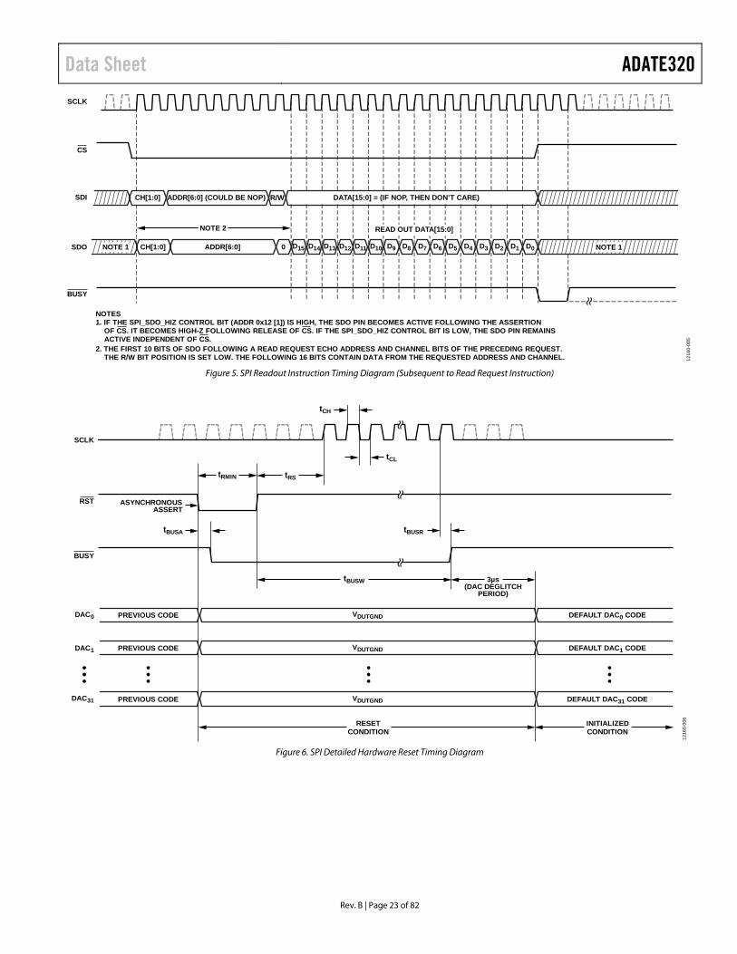
SCLK
CS
SDI
SDO
BUSY
CH[1:0] R/WADDR[6:0] (COULD BE NOP)
CH[1:0] ADDR[6:0] 0 D15 D14 D13 D12 D11 D10 D9 D8 D7 D6 D5 D4 D3 D2 D1 D0
DATA[15:0] = (IF NOP, THEN DON’T CARE)
NOTE 1
NOTE 2
NOTE 1
READ OUT DATA[15:0]
NOTES1. IF THE SPI_SDO_HIZ CONTROL BIT (ADDR 0x12 [1]) IS HIGH, THE SDO PIN BECOMES ACTIVE FOLLOWING THE ASSERTION OF CS. IT BECOMES HIGH-Z FOLLOWING RELEASE OF CS. IF THE SPI_SDO_HIZ CONTROL BIT IS LOW, THE SDO PIN REMAINS ACTIVE INDEPENDENT OF CS.2. THE FIRST 10 BITS OF SDO FOLLOWING A READ REQUEST ECHO ADDRESS AND CHANNEL BITS OF THE PRECEDING REQUEST. THE R/W BIT POSITION IS SET LOW. THE FOLLOWING 16 BITS CONTAIN DATA FROM THE REQUESTED ADDRESS AND CHANNEL. 12
160-
005
Figure 5. SPI Readout Instruction Timing Diagram (Subsequent to Read Request Instruction)
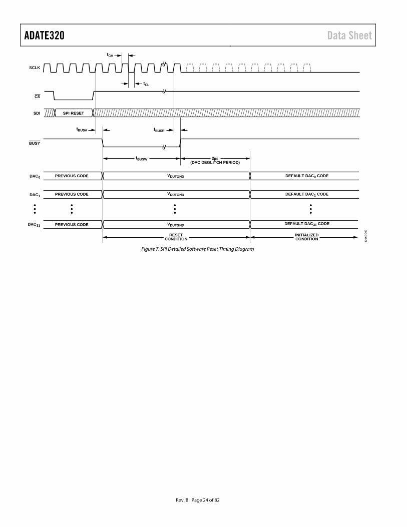
SCLK
RST
BUSY
DAC0 PREVIOUS CODE DEFAULT DAC0 CODEVDUTGND
PREVIOUS CODE DEFAULT DAC1 CODEVDUTGND
PREVIOUS CODE DEFAULT DAC31 CODE
INITIALIZEDCONDITION
RESETCONDITION
VDUTGND
DAC1
DAC31
tCH
ASYNCHRONOUSASSERT
tCL
tRStRMIN
tBUSA tBUSR
tBUSW 3µs(DAC DEGLITCH
PERIOD)
1216
0-00
6
Figure 6. SPI Detailed Hardware Reset Timing Diagram
ADATE320 Data Sheet
Rev. B | Page 24 of 82
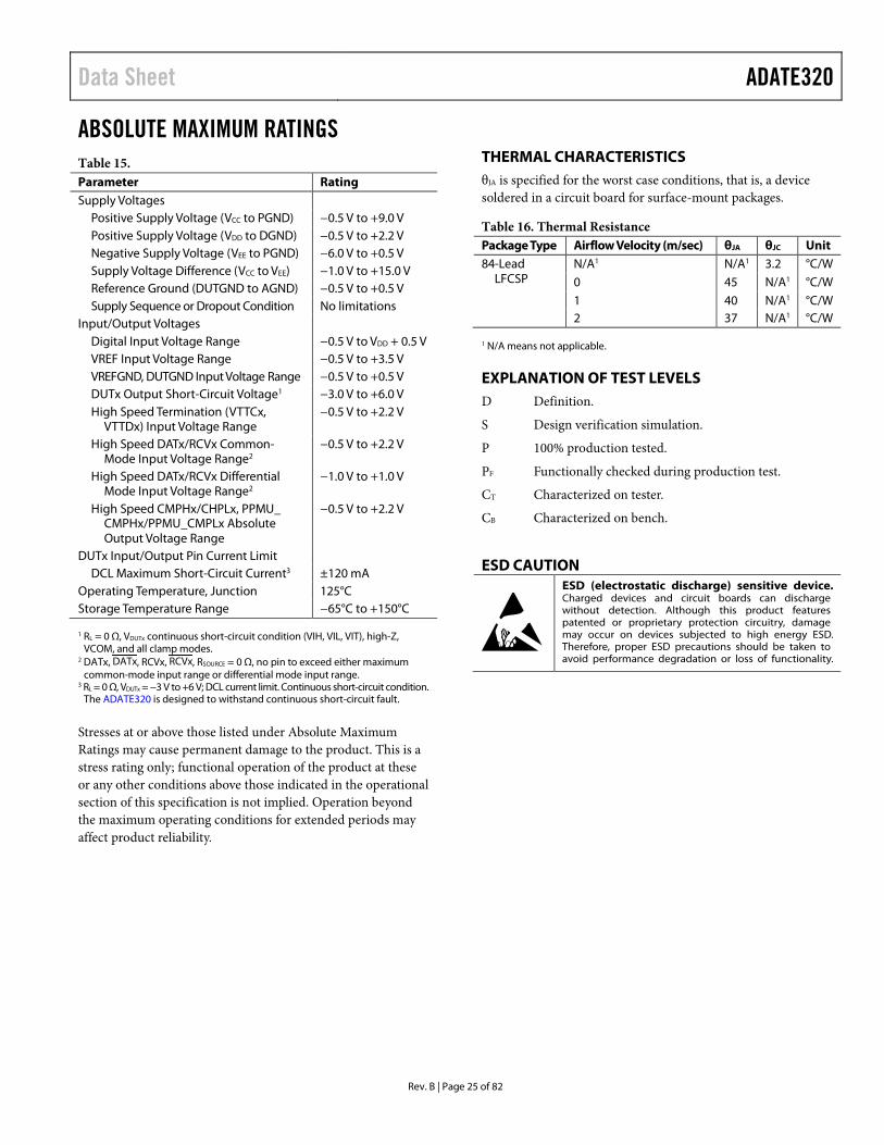
SCLK
CS
SDI SPI RESET
BUSY
DAC0
DAC1
DAC31
PREVIOUS CODE DEFAULT DAC0 CODEVDUTGND
PREVIOUS CODE DEFAULT DAC1 CODEVDUTGND
PREVIOUS CODE DEFAULT DAC31 CODE
INITIALIZEDCONDITION
RESETCONDITION
VDUTGND
tCH
tCL
tBUSA tBUSR
tBUSW 3µs(DAC DEGLITCH PERIOD)
1216
0-00
7
Figure 7. SPI Detailed Software Reset Timing Diagram
Data Sheet ADATE320
Rev. B | Page 25 of 82
ABSOLUTE MAXIMUM RATINGS Table 15. Parameter Rating Supply Voltages
Positive Supply Voltage (VCC to PGND) −0.5 V to +9.0 V Positive Supply Voltage (VDD to DGND) −0.5 V to +2.2 V Negative Supply Voltage (VEE to PGND) −6.0 V to +0.5 V Supply Voltage Difference (VCC to VEE) −1.0 V to +15.0 V Reference Ground (DUTGND to AGND) −0.5 V to +0.5 V Supply Sequence or Dropout Condition No limitations
Input/Output Voltages Digital Input Voltage Range −0.5 V to VDD + 0.5 V VREF Input Voltage Range −0.5 V to +3.5 V VREFGND, DUTGND Input Voltage Range −0.5 V to +0.5 V DUTx Output Short-Circuit Voltage1 −3.0 V to +6.0 V High Speed Termination (VTTCx,
VTTDx) Input Voltage Range −0.5 V to +2.2 V
High Speed DATx/RCVx Common-Mode Input Voltage Range2
−0.5 V to +2.2 V
High Speed DATx/RCVx Differential Mode Input Voltage Range2
−1.0 V to +1.0 V
High Speed CMPHx/CHPLx, PPMU_ CMPHx/PPMU_CMPLx Absolute Output Voltage Range
−0.5 V to +2.2 V
DUTx Input/Output Pin Current Limit DCL Maximum Short-Circuit Current3 ±120 mA
Operating Temperature, Junction 125°C Storage Temperature Range −65°C to +150°C 1 RL = 0 Ω, VDUTx continuous short-circuit condition (VIH, VIL, VIT), high-Z,
VCOM, and all clamp modes. 2 DATx, DATx, RCVx, RCVx, RSOURCE = 0 Ω, no pin to exceed either maximum
common-mode input range or differential mode input range. 3 RL = 0 Ω, VDUTx = −3 V to +6 V; DCL current limit. Continuous short-circuit condition.
The ADATE320 is designed to withstand continuous short-circuit fault.
Stresses at or above those listed under Absolute Maximum Ratings may cause permanent damage to the product. This is a stress rating only; functional operation of the product at these or any other conditions above those indicated in the operational section of this specification is not implied. Operation beyond the maximum operating conditions for extended periods may affect product reliability.
THERMAL CHARACTERISTICS θJA is specified for the worst case conditions, that is, a device soldered in a circuit board for surface-mount packages.
Table 16. Thermal Resistance Package Type Airflow Velocity (m/sec) θJA θJC Unit 84-Lead
LFCSP N/A1 N/A1 3.2 °C/W 0 45 N/A1 °C/W 1 40 N/A1 °C/W
2 37 N/A1 °C/W 1 N/A means not applicable.
EXPLANATION OF TEST LEVELS D Definition.
S Design verification simulation.
P 100% production tested.
PF Functionally checked during production test.
CT Characterized on tester.
CB Characterized on bench.
ESD CAUTION

ADATE320 Data Sheet
Rev. B | Page 26 of 82
USER INFORMATION AND TRUTH TABLES
Table 17. Driver Truth Table1 DRV Control Register High Speed Inputs2
Driver State DRIVE_ENABLE_x, Address 0x19, Bit 0
DRIVE_FORCE_x, Address 0x19, Bit 1
DRIVE_FORCE_STATE_x, Address 0x19, Bits[3:2]
DRIVE_VT_HIZ_x, Address 0x19, Bit 4 DATx RCVx
0 X XX X X X Low leakage 1 1 00 X X X Active VIL 1 1 01 X X X Active VIH 1 1 10 X X X Active high-Z 1 1 11 X X X Active VIT 1 0 XX 0 X 1 Active high-Z 1 0 XX 1 X 1 Active VIT 1 0 XX X 0 0 Active VIL 1 0 XX X 1 0 Active VIH 1 X means don’t care. 2 See Figure 139 for more detailed information about high speed DATx/RCVx input multiplexing.
Table 18. Comparator Truth Table
DMC_ENABLE, Address 0x1A, Bit 0
Comparator State CMPH0 State CMPL0 State CMPH1 State CMPL1 State
0 VDUT0 < VOH0 0 VDUT0 < VOL0 0 VDUT1 < VOH1 0 VDUT1 < VOL1 0 VOH0 < VDUT0 1 VOL0 < VDUT0 1 VOH1 < VDUT1 1 VOL1 < VDUT1 1
11 VDUT0 − VDUT1 < VOH0 0 VDUT0 − VDUT1 < VOL0 0 VDUT1 < VOH1 0 VDUT1 < VOL1 0 VOH0 < VDUT0 − VDUT1 1 VOL0 < VDUT0 − VDUT1 1 VOH1 < VDUT1 1 VOL1 < VDUT1 1
1 Note that the Channel 1 normal window comparator continues to function while the device is in differential compare mode, but at a greatly reduced bandwidth.
Table 19. Active Load Truth Table1 LOAD/DRV Control Registers High Speed Inputs2
Load State LOAD_ENABLE_x, Address 0x1B, Bit 0
LOAD_FORCE_x, Address 0x1B, Bit 1
DRIVE_VT_HIZ_x, Address 0x19, Bit 4 DATx RCVx
0 X X X X Low leakage 1 1 X X X Active on 1 0 X X 0 Active off 1 0 0 X 1 Active on 1 0 1 X 1 Active off 1 X means don’t care. 2 See Figure 139 for more detailed information about high speed DATx/RCVx input multiplexing.
Table 20. PPMU Go/No-Go Comparator Truth Table1 PPMU Control Register PPMU Go/No-Go Comparator State2
PPMU_ENABLE_x, Address 0x1C, Bit 0
PPMU_STANDBY_x, Address 0x1C, Bit 1 PPMU_CMPHx State PPMU_CMPLx State
0 X X 0 X 0 1 X PPMUx MV/MI < POHx 0 PPMUx MV/MI < POLx 0 1 X POHx < PPMUx MV/MI 1 POLx < PPMUx MV/MI 1 1 X means don’t care. 2 The PPMUx MV/MI inputs to the PPMU go/no-go comparators always come directly from the respective internal PPMU instrumentation amplifiers, not from the
PPMU_Mx output pins (see Figure 144). The internal instrumentation amplifiers are independently configured for either measure voltage (MV) or measure current (MI), depending on the settings of the PPMU_MEAS_VI_x control bit, as described in Figure 151. When PPMU power is not enabled, the respective go/no-go comparator outputs are locked to a static low state (see Table 21).
Data Sheet ADATE320
Rev. B | Page 27 of 82
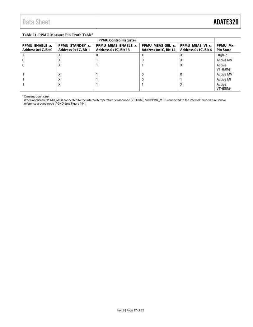
Table 21. PPMU Measure Pin Truth Table1 PPMU Control Register
PPMU_Mx, Pin State
PPMU_ENABLE_x, Address 0x1C, Bit 0
PPMU_STANDBY_x, Address 0x1C, Bit 1
PPMU_MEAS_ENABLE_x, Address 0x1C, Bit 13
PPMU_MEAS_SEL_x, Address 0x1C, Bit 14
PPMU_MEAS_VI_x, Address 0x1C, Bit 6
X X 0 X X High-Z 0 X 1 0 X Active MV 0 X 1 1 X Active
VTHERM2 1 X 1 0 0 Active MV 1 X 1 0 1 Active MI 1 X 1 1 X Active
VTHERM2 1 X means don’t care. 2 When applicable, PPMU_M0 is connected to the internal temperature sensor node (VTHERM), and PPMU_M1 is connected to the internal temperature sensor
reference ground node (AGND) (see Figure 144).
ADATE320 Data Sheet
Rev. B | Page 28 of 82
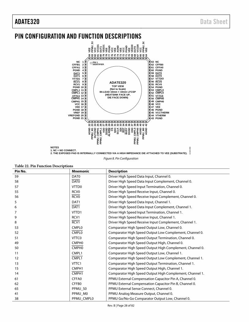
PIN CONFIGURATION AND FUNCTION DESCRIPTIONS
NOTES1. NC = NO CONNECT.2. THE EXPOSED PAD IS INTERNALLY CONNECTED VIA A HIGH IMPEDANCE DIE ATTACHED TO VEE (SUBSTRATE).
1NC2CFFB13CFFA14PGND5DAT16DAT17VTTD18RCV19RCV1
10PGND11CMPL112CMPL113VTTC114CMPH115CMPH116VCC17VEE18PGND19VREF20VREFGND
22A
GN
D23
PPM
U_M
124
DU
TGN
D25
PPM
U_C
MPH
126
PPM
U_C
MPL
127
VDD
28D
GN
D29
ALA
RM
30C
S31
SDO
32SC
LK33
SDI
34R
ST35
BU
SY36
DG
ND
37VD
D38
PPM
U_C
MPL
039
PPM
U_C
MPH
040
AG
ND
55 RCV056 RCV057 VTTDO58 DAT059 DAT060 PGND61 CFFA062 CFFB063 NC
54 PGND53 CMPL052 CMPL051 VTTC050 CMPH049 CMPH048 VCC47 VEE46 PGND45 VCCTHERM44 VTHERM43 PGND
75VE
E76
VCC
77PG
ND
78VE
E79
VEED
180
DU
T181
VCC
D1
82VC
C83
PPM
U_S
184
VEE
74A
GN
D73
VEE
72VC
C71
PGN
D70
VEE
69VE
ED0
68D
UT0
67VC
CD
066
VCC
65PP
MU
_S0
64VE
E
ADATE320TOP VIEW
(Not to Scale)84-LEAD 10mm × 10mm LFCSP
(HEATSINK FACE UP,DIE FACE DOWN)
21PGND
41PP
MU
_M0
42A
GN
D
PIN 1IDENTIFIER
1216
0-00
8
Figure 8. Pin Configuration
Table 22. Pin Function Descriptions Pin No. Mnemonic Description 59 DAT0 Driver High Speed Data Input, Channel 0. 58 DAT0 Driver High Speed Data Input Complement, Channel 0.
57 VTTD0 Driver High Speed Input Termination, Channel 0. 55 RCV0 Driver High Speed Receive Input, Channel 0. 56 RCV0 Driver High Speed Receive Input Complement, Channel 0.
5 DAT1 Driver High Speed Data Input, Channel 1. 6 DAT1 Driver High Speed Data Input Complement, Channel 1.
7 VTTD1 Driver High Speed Input Termination, Channel 1. 9 RCV1 Driver High Speed Receive Input, Channel 1. 8 RCV1 Driver High Speed Receive Input Complement, Channel 1.
53 CMPL0 Comparator High Speed Output Low, Channel 0. 52 CMPL0 Comparator High Speed Output Low Complement, Channel 0.
51 VTTC0 Comparator High Speed Output Termination, Channel 0. 49 CMPH0 Comparator High Speed Output High, Channel 0. 50 CMPH0 Comparator High Speed Output High Complement, Channel 0.
11 CMPL1 Comparator High Speed Output Low, Channel 1. 12 CMPL1 Comparator High Speed Output Low Complement, Channel 1.
13 VTTC1 Comparator High Speed Output Termination, Channel 1. 15 CMPH1 Comparator High Speed Output High, Channel 1. 14 CMPH1 Comparator High Speed Output High Complement, Channel 1.
61 CFFA0 PPMU External Compensation Capacitor Pin A, Channel 0. 62 CFFB0 PPMU External Compensation Capacitor Pin B, Channel 0. 65 PPMU_S0 PPMU External Sense Connect, Channel 0. 41 PPMU_M0 PPMU Analog Measure Output, Channel 0. 38 PPMU_CMPL0 PPMU Go/No-Go Comparator Output Low, Channel 0.

Data Sheet ADATE320
Rev. B | Page 29 of 82
Pin No. Mnemonic Description 39 PPMU_CMPH0 PPMU Go/No-Go Comparator Output High, Channel 0. 3 CFFA1 PPMU External Compensation Capacitor Pin A, Channel 1. 2 CFFB1 PPMU External Compensation Capacitor Pin B, Channel 1. 83 PPMU_S1 PPMU External Sense Connect, Channel 1. 23 PPMU_M1 PPMU Analog Measure Output, Channel 1. 26 PPMU_CMPL1 PPMU Go/No-Go Comparator Output Low, Channel 1. 25 PPMU_CMPH1 PPMU Go/No-Go Comparator Output High, Channel 1. 34 RST Reset Input (Active Low).
32 SCLK Serial Programmable Interface (SPI) Clock Input. 30 CS Serial Programmable Interface (SPI) Chip Select Input (Active Low).
33 SDI Serial Programmable Interface (SPI) Serial Data Input. 31 SDO Serial Programmable Interface (SPI) Serial Data Output. 29 ALARM Fault Alarm Open-Drain Output (Open-Collector, Active Low).
35 BUSY Serial Programmable Interface (SPI) Busy Output (Open-Collector, Active Low).
19 VREF DAC Precision 2.500 V Reference Input. 20 VREFGND DAC Precision 0.000 V Reference Input. 24 DUTGND DUT Ground Sense Input. 68 DUT0 DUT Pin, Channel 0. 80 DUT1 DUT Pin, Channel 1. 45 VCCTHERM Temperature Sensor VCC Supply (8.0 V). 44 VTHERM Temperature Sensor Analog Output. 16, 48, 66, 67, 72, 76, 81, 82 VCC, VCCD0, VCCD1 Analog Supply (8.0 V). 27, 37 VDD Digital Supply (1.8 V). 22, 40, 42, 74 AGND Analog Ground (Quiet). 28, 36 DGND Digital Ground. 4, 10, 18, 21, 43, 46, 54, 60, 71, 77 PGND Power Ground. 17, 47, 64, 69, 70, 73, 75, 78, 79, 84 VEE, VEED0, VEED1 Analog Supply (−5.0 V). 1, 63 NC No Connect. These pins can be grounded or left floating. EP Exposed Pad. The exposed pad is internally connected via a high impedance
die attached to VEE (substrate).

ADATE320 Data Sheet
Rev. B | Page 30 of 82
TYPICAL PERFORMANCE CHARACTERISTICS
3.5
–0.5
0
0.5
1.0
1.5
2.0
2.5
3.0
–2 –1 0 1 2 3 4 5
LEAK
AGE
(nA)
VDUTx (V) 1216
0-10
9
Figure 9. DUTx Pin Leakage in High-Z Mode
0.35
0
0.05
0.10
0.15
0.20
0.25
0.30
–2 –1 0 1 2 3 4 5
LEAK
AGE
(nA)
VDUTx (V) 1216
0-11
0
Figure 10. DUTx Pin Leakage in Low Leakage Mode
–60 –40 –30 0 20 40 60
DRIV
ER O
UTPU
T RE
SIST
ANCE
(Ω)
DRIVER OUTPUT CURRENT (mA)
46.0
46.5
47.0
47.5
48.0
48.5
49.0
49.5
50.0
50.5
51.0
1216
0-11
1
Figure 11. Driver Output Resistance vs. Driver Output Current
54 56 58 60 62 64 66
IMPE
DANC
E (5
Ω/D
IV)
TIME (ns)
30
70
55
60
65
50
45
40
35
1216
0-11
2
Figure 12. DUTx Pin Time-Domain Reflectometry (TDR) Response
0 1 2 3 4 5 6 7 8
DRIV
ER O
FFSE
T (m
V)
DRIVER CLC SETTING, 3-BIT VALUE
–6
2
–1
0
1
–2
–3
–4
–5
VILVIHVIT
1216
0-11
3
Figure 13. Driver Offset vs. Driver CLC Setting, 3-Bit Value
–2 0–1 1 2 3 4 5
LINE
ARIT
Y ER
ROR
(mV)
DRIVER OUTPUT VOLTAGE (V)
–8
8
2
4
6
0
–2
–4
–6
1216
0-11
4
Figure 14. Driver VIH INL

Data Sheet ADATE320
Rev. B | Page 31 of 82
–2 0–1 1 2 3 4 5
LINE
ARIT
Y ER
ROR
(mV)
DRIVER OUTPUT VOLTAGE (V)
–8
8
2
4
6
0
–2
–4
–6
1216
0-11
5
Figure 15. Driver VIL INL
–2 0–1 1 2 3 4 5
LINE
ARIT
Y ER
ROR
(mV)
DRIVER OUTPUT VOLTAGE (V)
–8
8
2
4
6
0
–2
–4
–6
1216
0-11
6
Figure 16. Driver VIT INL
–2 –1 0 1 2 3 4 5
VIH
INTE
RACT
ION
ERRO
R (m
V)
VIL PROGRAMMED DAC VOLTAGE (V)
–2.0
2.0
0.5
1.0
1.5
0
–0.5
–1.0
–1.5
1216
0-11
7
Figure 17. Driver VIH Interaction Error vs. VIL Programmed DAC Voltage
–2 –1 0 1 2 3 4 5
VIL
INTE
RACT
ION
ERRO
R (m
V)
VIH PROGRAMMED DAC VOLTAGE (V)
–2.0
2.0
0.5
1.0
1.5
0
–0.5
–1.0
–1.5
1216
0-11
8
Figure 18. Driver VIL Interaction Error vs. VIH Programmed DAC Voltage
–2 –1 0 1 2 3 4 5
VIT
INTE
RACT
ION
ERRO
R (m
V)
VIL PROGRAMMED DAC VOLTAGE (V)
–2.0
2.0
0.5
1.0
1.5
0
–0.5
–1.0
–1.5
1216
0-11
9
Figure 19. Driver VIT Interaction Error vs. VIH Programmed DAC Voltage
–2 –1 0 1 2 3 4 5
VIT
INTE
RACT
ION
ERRO
R (m
V)
VIL PROGRAMMED DAC VOLTAGE (V)
–2.0
2.0
0.5
1.0
1.5
0
–0.5
–1.0
–1.5
1216
0-12
0
Figure 20. Driver VIT Interaction Error vs. VIL Programmed DAC Voltage

ADATE320 Data Sheet
Rev. B | Page 32 of 82
–3 –2 –1 0 4321 5 6
DRIV
ER O
UTPU
T CU
RREN
T (m
A)
VDUTx (V)
–100
–80
–60
–40
–20
0
20
1216
0-12
1
Figure 21. Driver Output Current Limit, Sink
–3 –2 –1 0 4321 5 6
DRIV
ER O
UTPU
T CU
RREN
T (m
A)
VDUTx (V)
–20
0
20
40
60
80
100
1216
0-12
2
Figure 22. Driver Output Current Limit, Source
38 39 40 41 42 43 44 45 46 47
VOLT
AGE
(V)
TIME (ns)
–0.02
0.12
0.10
0.08
0.06
0.04
0.02
0
50mV RISE50mV FALL100mV RISE100mV FALL200mV RISE200mV FALL
1216
0-12
3
Figure 23. Driver Small Swing Response
38 39 40 41 42 43 44 45 46 47
VOLT
AGE
(V)
TIME (ns)
–0.2
1.6
1.4
1.2
1.0
0.8
0.6
0.4
0.2
0
1V RISE1V FALL2V RISE2V FALL3V RISE3V FALL
1216
0-12
4
Figure 24. Driver Large Swing Response
38 40 42 44 46 48
VOLT
AGE
(V)
TIME (ns)
–0.02
0.14
0.12
0.10
0.08
0.06
0.04
0.02
0
50mV100mV200mV
1216
0-12
5
Figure 25. Driver 100 MHz Response, Small Swing
38 43 48 53 58
VOLT
AGE
(V)
TIME (ns)
–0.2
1.8
1.6
1.4
1.2
1.0
0.8
0.6
0.4
0.2
0
1V2V3V
1216
0-12
6
Figure 26. Driver 100 MHz Response, Large Swing

Data Sheet ADATE320
Rev. B | Page 33 of 82
38.0 38.5 39.0 39.5 40.540.0 41.0
VOLT
AG
E (V
)
TIME (ns)
–0.02
0.14
0.12
0.10
0.08
0.06
0.04
0.02
0
50mV100mV200mV
1216
0-12
7
Figure 27. Driver 800 MHz Response, Small Swing
38.0 38.5 39.0 39.5 40.540.0 41.0
VOLT
AG
E (V
)
TIME (ns)
–0.2
1.8
1.6
1.4
1.2
1.0
0.8
0.6
0.4
0.2
0
1V2V3V
1216
0-12
8
Figure 28. Driver 800 MHz Response, Large Swing
38.0 38.5 39.0 39.5 40.0
VOLT
AG
E (V
)
TIME (ns)
–0.02
0.14
0.12
0.10
0.08
0.06
0.04
0.02
0
50mV100mV200mV
1216
0-12
9
Figure 29. Driver 1.25 GHz Response, Small Swing
38.0 38.5 39.0 39.5 40.0
VOLT
AG
E (V
)
TIME (ns)
–0.2
1.8
1.6
1.4
1.2
1.0
0.8
0.6
0.4
0.2
0
1V2V3V
1216
0-13
0
Figure 30. Driver 1.25 GHz Response, Large Swing
38.5 40.5 42.5 44.5 46.5 48.5 50.5 52.5
VOLT
AG
E (V
)
TIME (ns)
–0.2
1.2
1.0
0.8
0.6
0.4
0.2
0
VIH TO/FROM VIT
VIL TO/FROM VIT
1216
0-13
1
Figure 31. Driver VIL/VIH to/from VIT, VIH = 2.0 V, VIL = 0.0 V, VIT = 1.0 V; 50 Ω
Terminated
39 41 43 45 47 49 51 53
VOLT
AG
E (V
)
TIME (ns)
–1.0
–0.8
–0.6
–0.4
–0.2
0
0.2
0.4
0.6
0.8
1.0
VIH TO/FROM HIGH-Z
VIL TO/FROM HIGH-Z
1216
0-13
2
Figure 32. Driver VIL/VIH to/from High-Z, VIH = 1.0 V, VIL = −1.0 V; 50 Ω
Terminated
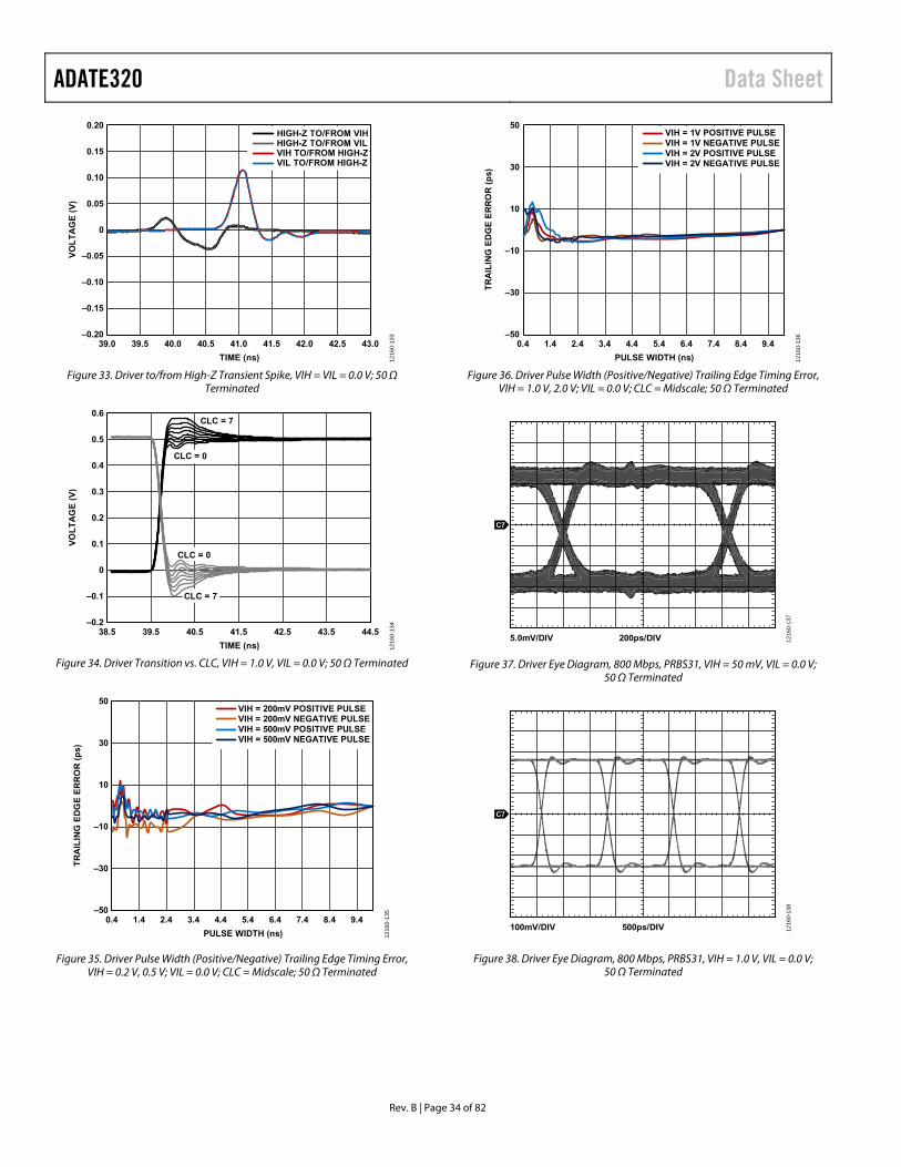
ADATE320 Data Sheet
Rev. B | Page 34 of 82
39.0 39.5 40.0 40.5 41.0 41.5 42.0 42.5 43.0
VO
LT
AG
E (
V)
TIME (ns)
–0.20
–0.15
–0.10
–0.05
0
0.05
0.10
0.15
0.20HIGH-Z TO/FROM VIHHIGH-Z TO/FROM VILVIH TO/FROM HIGH-ZVIL TO/FROM HIGH-Z
1216
0-13
3
Figure 33. Driver to/from High-Z Transient Spike, VIH = VIL = 0.0 V; 50 Ω Terminated
38.5 39.5 40.5 41.5 42.5 43.5 44.5
VO
LT
AG
E (
V)
TIME (ns)
–0.2
–0.1
0
0.1
0.2
0.3
0.4
0.5
0.6
CLC = 0
CLC = 7
CLC = 0
CLC = 7
1216
0-13
4
Figure 34. Driver Transition vs. CLC, VIH = 1.0 V, VIL = 0.0 V; 50 Ω Terminated
0.4 9.48.47.46.45.44.43.42.41.4
TR
AIL
ING
ED
GE
ER
RO
R (
ps)
PULSE WIDTH (ns)
–50
–30
–10
10
30
50VIH = 200mV POSITIVE PULSEVIH = 200mV NEGATIVE PULSEVIH = 500mV POSITIVE PULSEVIH = 500mV NEGATIVE PULSE
1216
0-13
5
Figure 35. Driver Pulse Width (Positive/Negative) Trailing Edge Timing Error, VIH = 0.2 V, 0.5 V; VIL = 0.0 V; CLC = Midscale; 50 Ω Terminated
0.4 9.48.47.46.45.44.43.42.41.4
TR
AIL
ING
ED
GE
ER
RO
R (
ps)
PULSE WIDTH (ns)
–50
–30
–10
10
30
50VIH = 1V POSITIVE PULSEVIH = 1V NEGATIVE PULSEVIH = 2V POSITIVE PULSEVIH = 2V NEGATIVE PULSE
1216
0-13
6
Figure 36. Driver Pulse Width (Positive/Negative) Trailing Edge Timing Error, VIH = 1.0 V, 2.0 V; VIL = 0.0 V; CLC = Midscale; 50 Ω Terminated
5.0mV/DIV 200ps/DIV
C7
1216
0-13
7
Figure 37. Driver Eye Diagram, 800 Mbps, PRBS31, VIH = 50 mV, VIL = 0.0 V; 50 Ω Terminated
100mV/DIV 500ps/DIV
C7
1216
0-13
8
Figure 38. Driver Eye Diagram, 800 Mbps, PRBS31, VIH = 1.0 V, VIL = 0.0 V; 50 Ω Terminated
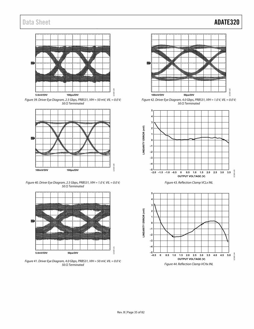
Data Sheet ADATE320
Rev. B | Page 35 of 82
5.0mV/DIV 100ps/DIV
C7
1216
0-13
9
Figure 39. Driver Eye Diagram, 2.5 Gbps, PRBS31, VIH = 50 mV, VIL = 0.0 V; 50 Ω Terminated
100mV/DIV 100ps/DIV
C7
1216
0-14
0
Figure 40. Driver Eye Diagram, 2.5 Gbps, PRBS31, VIH = 1.0 V, VIL = 0.0 V; 50 Ω Terminated
5.0mV/DIV 50ps/DIV
C7
1216
0-14
1
Figure 41. Driver Eye Diagram, 4.0 Gbps, PRBS31, VIH = 50 mV, VIL = 0.0 V; 50 Ω Terminated
100mV/DIV 50ps/DIV
C7
1216
0-14
2
Figure 42. Driver Eye Diagram, 4.0 Gbps, PRBS31, VIH = 1.0 V, VIL = 0.0 V; 50 Ω Terminated
LIN
EA
RIT
Y E
RR
OR
(m
V)
OUTPUT VOLTAGE (V)
–5
–4
–3
–2
–1
0
1
2
3
4
5
–2.0 –1.0 3.53.02.01.00–1.5 2.51.50.5–0.5
1216
0-14
3
Figure 43. Reflection Clamp VCLx INL
LIN
EA
RIT
Y E
RR
OR
(m
V)
OUTPUT VOLTAGE (V)
–5
–4
–3
–2
–1
0
1
2
3
4
5
–0.5 5.04.54.03.53.02.01.00 2.51.50.5
1216
0-14
4
Figure 44. Reflection Clamp VCHx INL
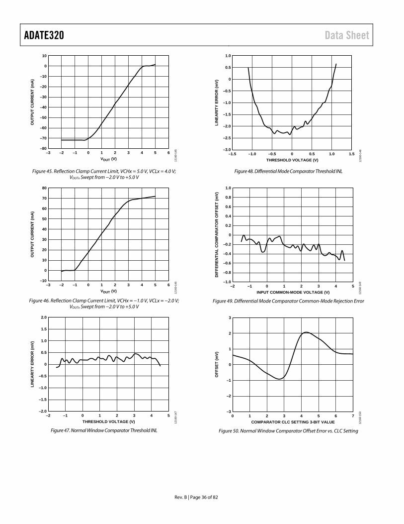
ADATE320 Data Sheet
Rev. B | Page 36 of 82
OUT
PUT
CURR
ENT
(mA)
VDUT (V)
–80
–70
–60
–50
–40
–30
–20
–10
0
10
–3 –2 –1 0 1 2 3 4 5 6
1216
0-14
5
Figure 45. Reflection Clamp Current Limit, VCHx = 5.0 V, VCLx = 4.0 V; VDUTx Swept from −2.0 V to +5.0 V
OUT
PUT
CURR
ENT
(mA)
VDUT (V)
–10
0
10
20
30
40
50
60
70
80
–3 –2 –1 0 1 2 3 4 5 6
1216
0-14
6
Figure 46. Reflection Clamp Current Limit, VCHx = −1.0 V, VCLx = −2.0 V;
VDUTx Swept from −2.0 V to +5.0 V
LINE
ARIT
Y ER
ROR
(mV)
THRESHOLD VOLTAGE (V)
–2.0
–1.5
–1.0
–0.5
0
0.5
1.0
1.5
2.0
–2 –1 543210
1216
0-14
7
Figure 47. Normal Window Comparator Threshold INL
LIN
EAR
ITY
ERR
OR
(mV)
THRESHOLD VOLTAGE (V)
–3.0
–2.5
–2.0
–1.5
–1.0
–0.5
0
0.5
1.0
–1.5 –1.0 1.51.00.50–0.5
1216
0-14
8
Figure 48. Differential Mode Comparator Threshold INL
DIFF
EREN
TIAL
CO
MPA
RATO
R O
FFSE
T (m
V)
INPUT COMMON-MODE VOLTAGE (V)
–1.0
–0.8
–0.6
–0.4
–0.2
0
0.2
0.4
0.6
0.8
1.0
–2 –1 53 4210
1216
0-14
9
Figure 49. Differential Mode Comparator Common-Mode Rejection Error
OFF
SET
(mV)
COMPARATOR CLC SETTING 3-BIT VALUE
–3
3
2
1
0
–1
–2
0 1 2 3 4 5 6 7
1216
0-15
0
Figure 50. Normal Window Comparator Offset Error vs. CLC Setting

Data Sheet ADATE320
Rev. B | Page 37 of 82
OFF
SET
(mV)
DIFFERENTIAL COMPARATOR CLC SETTING 3-BIT VALUE
–3
3
2
1
0
–1
–2
0 1 2 3 4 5 6 7
1216
0-15
1
Figure 51. Differential Mode Comparator Offset Error vs. CLC Setting
MEA
SURE
D HY
STER
ESIS
(mV)
PROGRAMMED HYSTERESIS VALUE
–20
140
120
100
80
60
40
20
0
0 1 2 3 4 5 6 7 8 9 10 11 12 13 14 15
VOL, SINGLE-ENDED, CH0VOL, SINGLE-ENDED, CH1VOH, SINGLE-ENDED, CH0VOH, SINGLE-ENDED, CH1
1216
0-15
2
Figure 52. Normal Window Comparator Hysteresis vs. Programmed Hysteresis Value
MEA
SURE
D HY
STER
ESIS
(mV)
PROGRAMMED HYSTERESIS VALUE
–50
250
200
150
100
50
0
0 1 2 3 4 5 6 7 8 9 10 11 12 13 14 15
VOH, DIFFERENTIAL, CH0VOL, DIFFERENTIAL, CH0
1216
0-15
3
Figure 53. Differential Mode Comparator Hysteresis vs. Programmed
Hysteresis Value
VOLT
AGE
(V)
TIME (ns)
0.6
1.3
1.2
1.1
1.0
0.9
0.8
0.7
60 61 62 63 64 65 66
1216
0-15
4
CMPHx/CMPLxCMPHx/CMPLx
Figure 54. Comparator CML Output Waveform (ADATE320)
VOLT
AGE
(V)
TIME (ns)
0.6
1.3
1.2
1.1
1.0
0.9
0.8
0.7
60 61 62 63 64 65 66
1216
0-15
5
CMPHx/CMPLxCMPHx/CMPLx
Figure 55. Comparator CML Output Waveform (ADATE320-1)
TPD
ER
RO
R (p
s)
INPUT WAVEFORM RISE TIME (ns)
–50
–30
–10
10
30
50
0.4 1.00.90.80.70.60.5
FALLING EDGERISING EDGE
1216
0-15
6
Figure 56. Normal Window Comparator Propagation Delay vs. Input Rise
Time, 1.0 V Input Swing
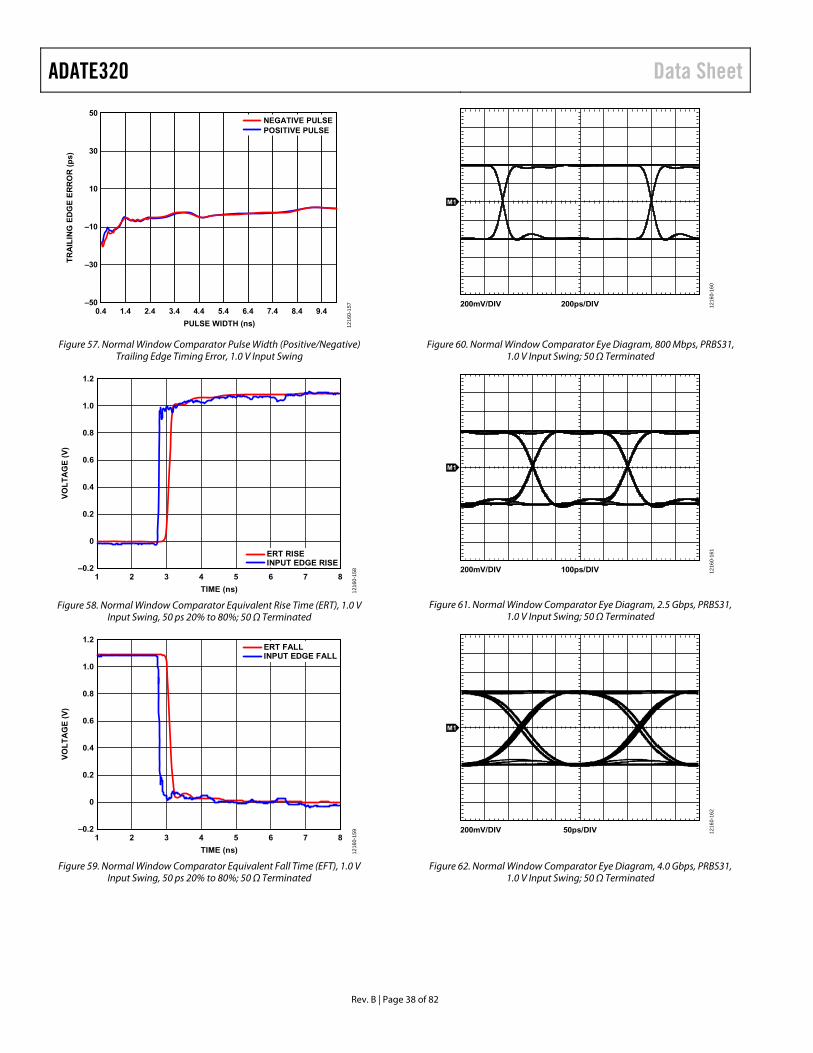
ADATE320 Data Sheet
Rev. B | Page 38 of 82
TR
AIL
ING
ED
GE
ER
RO
R (
ps)
PULSE WIDTH (ns)
–50
–30
–10
10
30
50
0.4 9.48.47.46.45.44.43.42.41.4
NEGATIVE PULSEPOSITIVE PULSE
1216
0-15
7
Figure 57. Normal Window Comparator Pulse Width (Positive/Negative) Trailing Edge Timing Error, 1.0 V Input Swing
VO
LT
AG
E (
V)
TIME (ns)
–0.2
1.2
1.0
0.8
0.6
0.4
0.2
0
1 2 3 4 5 6 7 8
ERT RISEINPUT EDGE RISE
1216
0-15
8
Figure 58. Normal Window Comparator Equivalent Rise Time (ERT), 1.0 V Input Swing, 50 ps 20% to 80%; 50 Ω Terminated
VO
LT
AG
E (
V)
TIME (ns)
–0.2
1.2
1.0
0.8
0.6
0.4
0.2
0
1 2 3 4 5 6 7 8
ERT FALLINPUT EDGE FALL
1216
0-15
9
Figure 59. Normal Window Comparator Equivalent Fall Time (EFT), 1.0 V Input Swing, 50 ps 20% to 80%; 50 Ω Terminated
200mV/DIV 200ps/DIV
M1
1216
0-16
0
Figure 60. Normal Window Comparator Eye Diagram, 800 Mbps, PRBS31, 1.0 V Input Swing; 50 Ω Terminated
200mV/DIV 100ps/DIV
M1
1216
0-16
1
Figure 61. Normal Window Comparator Eye Diagram, 2.5 Gbps, PRBS31, 1.0 V Input Swing; 50 Ω Terminated
200mV/DIV 50ps/DIV
M1
1216
0-16
2
Figure 62. Normal Window Comparator Eye Diagram, 4.0 Gbps, PRBS31, 1.0 V Input Swing; 50 Ω Terminated

Data Sheet ADATE320
Rev. B | Page 39 of 82
200mV/DIV 200ps/DIV
M1
1216
0-16
3
Figure 63. Differential Mode Comparator Eye Diagram, 800 Mbps, PRBS31, 1.0 V Input Swing; 50 Ω Terminated
200mV/DIV 100ps/DIV
M1
1216
0-16
4
Figure 64. Differential Mode Comparator Eye Diagram, 2.5 Gbps, PRBS31, 1.0 V Input Swing; 50 Ω Terminated
200mV/DIV 50ps/DIV
M1
1216
0-16
5
Figure 65. Differential Mode Comparator Eye Diagram, 4.0 Gbps, PRBS31, 1.0 V Input Swing; 50 Ω Terminated
LIN
EA
RIT
Y E
RR
OR
(m
V)
VCOM VOLTAGE (V)
–1.5
–1.0
–0.5
0
0.5
1.0
1.5
2.0
2.5
3.0
–2 –1 0 1 2 543
1216
0-16
6
Figure 66. Active Load VCOM INL
AC
TIV
E L
OA
D C
UR
RE
NT
(m
A)
PROGRAMMED CURRENT (mA)
0
25
20
15
10
5
0 5 10 15 20 25
LOAD CURRENT =DAC VOLTAGE/[2×(VREF – VREFGND)] × 25mA
~5mA/1V
1216
0-16
7
Figure 67. Active Load IOHx/IOLx Transfer Function
LIN
EA
RIT
Y E
RR
OR
(µ
A)
ACTIVE LOAD CURRENT (mA)
–40
–30
–20
–10
0
10
20
30
40
50
0 5 10 15 20 25
1216
0-16
8
Figure 68. Active Load IOHx INL
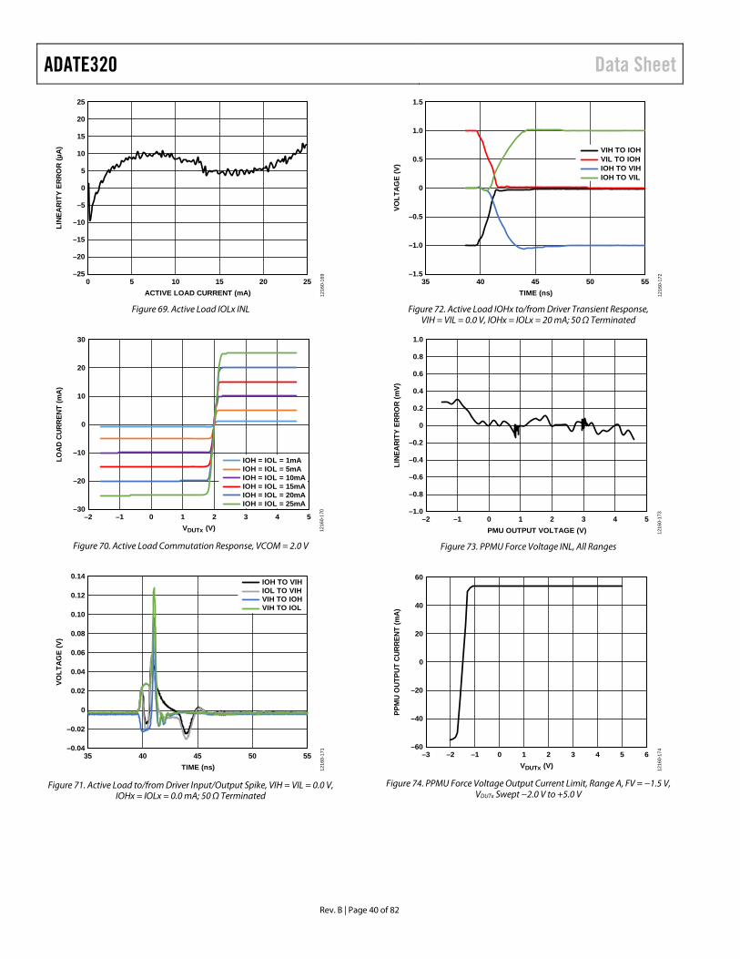
ADATE320 Data Sheet
Rev. B | Page 40 of 82
LINE
ARIT
Y ER
ROR
(µA)
ACTIVE LOAD CURRENT (mA)
–25
–20
–15
–10
–5
0
5
10
15
20
25
0 5 10 15 20 25
1216
0-16
9
Figure 69. Active Load IOLx INL
LOAD
CUR
RENT
(mA)
VDUTx (V)
–30
–20
–10
0
10
20
30
–2 –1 0 1 2 543
IOH = IOL = 1mAIOH = IOL = 5mAIOH = IOL = 10mAIOH = IOL = 15mAIOH = IOL = 20mAIOH = IOL = 25mA
1216
0-17
0
Figure 70. Active Load Commutation Response, VCOM = 2.0 V
VOLT
AGE
(V)
TIME (ns)
–0.04
–0.02
0
0.02
0.04
0.06
0.08
0.10
0.12
0.14
35 55504540
IOH TO VIHIOL TO VIHVIH TO IOHVIH TO IOL
1216
0-17
1
Figure 71. Active Load to/from Driver Input/Output Spike, VIH = VIL = 0.0 V, IOHx = IOLx = 0.0 mA; 50 Ω Terminated
VOLT
AGE
(V)
TIME (ns)
–1.5
–1.0
–0.5
0
0.5
1.0
1.5
35 55504540
VIH TO IOHVIL TO IOHIOH TO VIHIOH TO VIL
1216
0-17
2
Figure 72. Active Load IOHx to/from Driver Transient Response,
VIH = VIL = 0.0 V, IOHx = IOLx = 20 mA; 50 Ω Terminated
LINE
ARIT
Y ER
ROR
(mV)
PMU OUTPUT VOLTAGE (V)
–1.0
–0.8
–0.6
–0.4
–0.2
0
0.2
0.4
0.6
0.8
1.0
–2 –1 543210
1216
0-17
3
Figure 73. PPMU Force Voltage INL, All Ranges
PPM
U O
UTPU
T CU
RREN
T (m
A)
VDUTx (V)
–60
–40
–20
0
20
40
60
–3 –2 64 53210–1
1216
0-17
4
Figure 74. PPMU Force Voltage Output Current Limit, Range A, FV = −1.5 V,
VDUTx Swept −2.0 V to +5.0 V

Data Sheet ADATE320
Rev. B | Page 41 of 82
PPM
U O
UTPU
T CU
RREN
T (m
A)
VDUTx (V)
–80
–60
–40
–20
0
20
40
60
–3 –2 64 53210–1
1216
0-17
5
Figure 75. PPMU Force Voltage Output Current Limit, Range A, FV = 4.5 V,
VDUTx Swept −2.0 V to +5.0 V
PPM
U O
UTPU
T CU
RREN
T (m
A)
VDUTx (V)
–0.004
–0.003
–0.002
–0.001
0
0.001
0.002
0.003
0.004
–3 –2 64 53210–1
1216
0-17
6
Figure 76. PPMU Force Voltage Output Current Limit, Range E, FV = −1.5 V,
VDUTx Swept −2.0 V to +5.0 V
PPM
U O
UTPU
T CU
RREN
T (m
A)
VDUTx (V)
–0.004
–0.003
–0.002
–0.001
0
0.001
0.002
0.003
0.004
–3 –2 64 53210–1
1216
0-17
7
Figure 77. PPMU Force Voltage Output Current Limit, Range E, FV = 4.5 V,
VDUTx Swept −2.0 V to +5.0 V
ERRO
R (m
V)
IDUTx (mA)
–0.5
–0.4
–0.3
–0.2
–0.1
0
0.1
0.2
0.3
0.5
0.4
–40 –30 –20 –10 0 10 20 30 40
1216
0-17
8
Figure 78. PPMU Force Voltage Compliance Error, Range A, FV = −1.0 V vs.
Output Current, Internal Sense
ERRO
R (m
V)
IDUTx (mA)
–0.5
–0.4
–0.3
–0.2
–0.1
0
0.1
0.2
0.3
0.5
0.4
–40 –30 –20 –10 0 10 20 30 40
1216
0-17
9
Figure 79. PPMU Force Voltage Compliance Error, Range A, FV = 4.0 V vs.
Output Current (IDUTx) , Internal Sense
ERRO
R (m
V)
IDUTx (mA)
–0.5
–0.4
–0.3
–0.2
–0.1
0
0.1
0.2
0.3
0.5
0.4
–1.0 –0.8 –0.6 –0.4 0–0.2 0.2 0.4 0.6 0.8 1.0
1216
0-18
0
Figure 80. PPMU Force Voltage Compliance Error, Range B, FV = −1.5 V vs.
Output Current(IDUTx), Internal Sense

ADATE320 Data Sheet
Rev. B | Page 42 of 82
ERRO
R (m
V)
IDUTx (mA)
–0.5
–0.4
–0.3
–0.2
–0.1
0
0.1
0.2
0.3
0.5
0.4
–1.0 –0.8 –0.6 –0.4 0–0.2 0.2 0.4 0.6 0.8 1.0
1216
0-18
1
Figure 81. PPMU Force Voltage Compliance Error, Range B, FV = 4.5 V vs.
Output Current (IDUTx), Internal Sense
LINE
ARIT
Y ER
ROR
(µA)
PMU OUTPUT CURRENT (mA)
–25
–20
–15
–10
–5
0
5
10
15
25
20
–40 –30 –20 –10 0 10 20 30 40
1216
0-18
2
Figure 82. PPMU Force Current INL, Range A
LINE
ARIT
Y ER
ROR
(µA)
PMU OUTPUT CURRENT (mA)
–0.25
–0.20
–0.15
–0.10
–0.05
0
0.05
0.10
0.15
0.25
0.20
–1.0 –0.8 –0.6 –0.4 –0.2 0 0.2 0.4 0.6 0.8 1.0
1216
0-18
3
Figure 83. PPMU Force Current INL, Range B
LIN
EAR
ITY
ERR
OR
(µA
)
PMU OUTPUT CURRENT (mA)
–0.025
–0.020
–0.015
–0.010
–0.005
0
0.005
0.010
0.015
0.025
0.020
–1.0 –0.8 –0.6 –0.4 –0.2 0 0.2 0.4 0.6 0.8 1.0
1216
0-18
4
Figure 84. PPMU Force Current INL, Range C
LIN
EAR
ITY
ERR
OR
(µA
)
PMU OUTPUT CURRENT (mA)
–0.0025
–0.0015
–0.0005
0.0005
0.0015
0.0025
–0.010 –0.005 0 0.005 0.010
1216
0-18
5
Figure 85. PPMU Force Current INL, Range D
LIN
EAR
ITY
ERR
OR
(µA
)
PMU OUTPUT CURRENT (mA)
–0.0005
–0.0003
–0.0001
0.0001
0.0003
0.0005
–0.0020 –0.0010 0 0.0010 0.0020
1216
0-18
6
Figure 86. PPMU Force Current INL, Range E

Data Sheet ADATE320
Rev. B | Page 43 of 82
ERR
OR
(µA
)
VDUTx (V)
–30
–20
–10
10
0
20
30
50
40
–2 –1 543210
1216
0-18
7
Figure 87. PPMU Force Current Compliance Error, Range A, FI = −40 mA vs.
Output Voltage (VDUTx)
ERR
OR
(µA
)
VDUTx (V)
–20
–15
–10
0
–5
5
10
20
15
–2 –1 543210
1216
0-18
8
Figure 88. PPMU Force Current Compliance Error, Range A, FI = 40 mA vs.
Output Voltage (VDUTx)
ERR
OR
(µA
)
VDUTx (V)
–0.5
–0.3
–0.4
–0.2
–0.1
0.1
0
0.2
0.3
0.5
0.4
–2 –1 543210
1216
0-18
9
Figure 89. PPMU Force Current Compliance Error, Range B, FI = −1 mA vs.
Output Voltage (VDUTx)
ERR
OR
(µA
)
VDUTx (V)
–0.5
–0.3
–0.4
–0.2
–0.1
0.1
0
0.2
0.3
0.5
0.4
–2 –1 543210
1216
0-19
0
Figure 90. PPMU Force Current Compliance Error, Range B, FI = 1 mA vs.
Output Voltage (VDUTx)
ERR
OR
(µA
)
VDUTx (V)
–0.05
–0.03
–0.04
–0.02
–0.01
0.01
0
0.02
0.03
0.05
0.04
–2 –1 543210
1216
0-19
1
Figure 91. PPMU Force Current Compliance Error, Range C, FI = −100 µA vs.
Output Voltage (VDUTx)
ERRO
R (µ
A)
VDUTx (V)
–0.05
–0.03
–0.04
–0.02
–0.01
0.01
0
0.02
0.03
0.05
0.04
–2 –1 543210
1216
0-19
2
Figure 92. PPMU Force Current Compliance Error, Range C, FI = 100 µA vs.
Output Voltage (VDUTx)

ADATE320 Data Sheet
Rev. B | Page 44 of 82
ERR
OR
(µA
)
VDUTx (V)
–0.0010
0
–0.0005
0.0005
0.0010
–2 –1 543210
1216
0-19
3
Figure 93. PPMU Force Current Compliance Error, Range E, FI = −2 µA vs.
Output Voltage (VDUTx)
ERR
OR
(µA
)
VDUTx (V)
–0.0010
0
–0.0005
0.0005
0.0010
–2 –1 543210
1216
0-19
4
Figure 94. PPMU Force Current Compliance Error, Range E, FI = 2 µA vs.
Output Voltage (VDUTx)
LIN
EAR
ITY
ERR
OR
(mV)
OUTPUT VOLTAGE (V)
–2.0
–1.5
–1.0
–0.5
0
0.5
1.0
–1.5 –1.0 –0.5 0 0.5 1.0 1.5 2.0 2.5 3.0 3.5
1216
0-19
5
Figure 95. PPMU Voltage Clamp PCLx INL
LIN
EAR
ITY
ERR
OR
(mV)
OUTPUT VOLTAGE (V)
–2.0
–1.5
–1.0
–0.5
0
0.5
1.0
–0.5 0 0.5 1.0 1.5 2.0 2.5 3.0 4.54.03.5
1216
0-19
6
Figure 96. PPMU Voltage Clamp PCHx INL
LINE
ARIT
Y ER
ROR
(µA)
OUTPUT CURRENT (mA)
–20
–15
–10
–5
0
5
10
15
20
–40 –35 –30 –25 –20 –15 –10 –5 0
1216
0-19
7
Figure 97. PPMU Current Clamp PCLx INL, Range A
LINE
ARIT
Y ER
ROR
(µA)
OUTPUT CURRENT (mA)
–20
–15
–10
–5
0
5
10
15
20
0 5 10 15 20 25 30 35 40
1216
0-19
8
Figure 98. PPMU Current Clamp PCHx INL, Range A
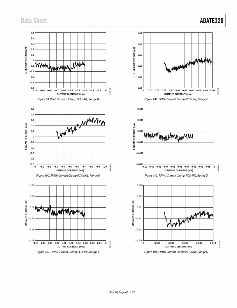
Data Sheet ADATE320
Rev. B | Page 45 of 82
LINE
ARIT
Y ER
ROR
(µA)
OUTPUT CURRENT (mA)
–0.5
–0.4
–0.3
–0.2
–0.1
0
0.5
0.4
0.3
0.2
0.1
–1.0 –0.9 –0.8 –0.7 –0.6 –0.5 –0.4 –0.3 –0.2 –0.1 0
1216
0-19
9
Figure 99. PPMU Current Clamp PCLx INL, Range B
LIN
EAR
ITY
ERR
OR
(µA
)
OUTPUT CURRENT (mA)
–0.5
–0.4
–0.3
–0.2
–0.1
0
0.5
0.4
0.3
0.2
0.1
0 0.1 0.2 0.3 0.4 0.5 0.6 0.7 0.8 0.9 1.0
1216
0-20
0
Figure 100. PPMU Current Clamp PCHx INL, Range B
LINE
ARIT
Y ER
ROR
(µA)
OUTPUT CURRENT (mA)
–0.05
–0.03
–0.01
0.05
0.03
0.01
–0.10 –0.09 –0.08 –0.07 –0.06 –0.05 –0.04 –0.03 –0.02 –0.01 0
1216
0-20
1
Figure 101. PPMU Current Clamp PCLx INL, Range C
LIN
EAR
ITY
ERR
OR
(µA
)
OUTPUT CURRENT (mA)
–0.05
–0.03
–0.01
0.05
0.03
0.01
0 0.01 0.02 0.03 0.04 0.05 0.06 0.07 0.08 0.09 0.10
1216
0-20
2
Figure 102. PPMU Current Clamp PCHx INL, Range C
LIN
EAR
ITY
ERR
OR
(µA
)
OUTPUT CURRENT (mA)
–0.005
–0.003
–0.001
0.005
0.003
0.001
–0.10 –0.09 –0.08 –0.07 –0.06 –0.05 –0.04 –0.03 –0.02 –0.01 0
1216
0-20
3
Figure 103. PPMU Current Clamp PCLx INL, Range D
LIN
EAR
ITY
ERR
OR
(µA
)
OUTPUT CURRENT (mA)
–0.005
–0.003
–0.001
0.005
0.003
0.001
0 0.002 0.004 0.006 0.008 0.010
1216
0-20
4
Figure 104. PPMU Current Clamp PCHx INL, Range D

ADATE320 Data Sheet
Rev. B | Page 46 of 82
LIN
EAR
ITY
ERR
OR
(µA
)
OUTPUT CURRENT (mA)
–0.0010
–0.0005
0
0.0010
0.0005
–0.0020 –0.0015 –0.0010 –0.0005 0
1216
0-20
5
Figure 105. PPMU Current Clamp PCLx INL, Range E
LIN
EAR
ITY
ERR
OR
(µA
)
OUTPUT CURRENT (mA)
–0.0010
–0.0005
0
0.0010
0.0005
0 0.0005 0.0010 0.0015 0.0020
1216
0-20
6
Figure 106. PPMU Current Clamp PCHx INL, Range E
LINE
ARIT
Y ER
ROR
(mV)
VDUTx (V)
–0.10
–0.08
–0.06
–0.04
–0.02
0
0.02
0.04
0.06
0.08
0.10
–2 –1 0 1 2 3 4 5
1216
0-20
7
Figure 107. PPMU Measure Voltage INL, Range B
LINE
ARIT
Y ER
ROR
(µA)
IDUTx (mA)
–0.10
–0.08
–0.06
–0.04
–0.02
0
0.02
0.04
0.06
0.08
0.10
–1.0 –0.8 –0.6 –0.4 –0.2 0 0.2 0.4 0.6 0.8 1.0
1216
0-20
8
Figure 108. PPMU Measure Current INL, Range B
PPM
U M
EASU
RE P
IN C
MRR
(mV)
VDUTx (V)
–0.50
–0.45
–0.40
–0.35
–0.30
–0.25
–0.20
–0.15
–0.10
–0.05
0
–1.0 –0.5 4.03.53.02.52.01.51.00.50
1216
0-20
9
Figure 109. PPMU Measure Current Common-Mode Rejection Error, Force
Voltage Measure Current (FVMI), Source 0.5 mA
VOLT
AGE
(V)
TIME (µs)
–0.1
0.6
0.5
0.4
0.3
0.2
0.1
0
0 5 10 15 20
RANGE A RISERANGE A FALL
1216
0-21
0
Figure 110. PPMU Force Voltage Transient Response, Range A, 0.0 V to 0.5 V,
Uncalibrated, CLOAD = 200 pF

Data Sheet ADATE320
Rev. B | Page 47 of 82
VOLT
AGE
(V)
TIME (µs)
–0.1
0.6
0.5
0.4
0.3
0.2
0.1
0
0 5 10 15 20
RANGE B RISERANGE B FALL
1216
0-21
1
Figure 111. PPMU Force Voltage Transient Response, Range B, 0.0 V to 0.5 V,
Uncalibrated, CLOAD = 200 pF
VOLT
AGE
(V)
TIME (µs)
–0.1
0.6
0.5
0.4
0.3
0.2
0.1
0
0 10 20 30 5040
RANGE C RISERANGE C FALL
1216
0-21
2
Figure 112. PPMU Force Voltage Transient Response, Range C, 0.0 V to 0.5 V,
Uncalibrated, CLOAD = 200 pF
VOLT
AGE
(V)
TIME (µs)
–0.1
0.6
0.5
0.4
0.3
0.2
0.1
0
0 5 10 15 20
RANGE A RISERANGE A FALL
1216
0-21
3
Figure 113. PPMU Force Voltage Transient Response, Range A, 0.0 V to 0.5 V,
Uncalibrated, CLOAD = 2000 pF
VOLT
AGE
(V)
TIME (µs)
–0.2
–0.1
0.7
0.6
0.5
0.4
0.3
0.2
0.1
0
0 5 10 15 20
RANGE B RISERANGE B FALL
1216
0-21
4
Figure 114. PPMU Force Voltage Transient Response, Range B, 0.0 V to 0.5 V,
Uncalibrated, CLOAD = 2000 pF
VOLT
AGE
(V)
TIME (µs)
–0.2
–0.1
0.7
0.6
0.5
0.4
0.3
0.2
0.1
0
0 605040302010
RANGE C RISERANGE C FALL
1216
0-21
5
Figure 115. PPMU Force Voltage Transient Response, Range C, 0.0 V to 0.5 V,
Uncalibrated, CLOAD = 2000 pF
VOLT
AGE
(V)
TIME (µs)
–0.1
4.9
4.4
3.9
3.4
2.9
2.4
1.9
1.4
0.9
0.4
0 8070605040302010
RANGE A RISERANGE A FALL
1216
0-21
6
Figure 116. PPMU Force Voltage Transient Response, Range A, 0.0 V to 4.0 V,
Uncalibrated, CLOAD = 200 pF

ADATE320 Data Sheet
Rev. B | Page 48 of 82
VOLT
AGE
(V)
TIME (µs)
–0.1
4.9
4.4
3.9
3.4
2.9
2.4
1.9
1.4
0.9
0.4
0 8070605040302010
RANGE B RISERANGE B FALL
1216
0-21
7
Figure 117. PPMU Force Voltage Transient Response, Range B, 0.0 V to 4.0 V,
Uncalibrated, CLOAD = 200 pF
VOLT
AG
E (V
)
TIME (µs)
–0.1
4.9
4.4
3.9
3.4
2.9
2.4
1.9
1.4
0.9
0.4
50 70 90 110 130 150
RANGE C RISERANGE C FALL
1216
0-21
8
Figure 118. PPMU Force Voltage Transient Response, Range C, 0.0 V to 4.0 V,
Uncalibrated, CLOAD = 200 pF
VOLT
AG
E (V
)
TIME (µs)
–0.1
4.9
4.4
3.9
3.4
2.9
2.4
1.9
1.4
0.9
0.4
0 20 140120100806040
RANGE A RISERANGE A FALL
1216
0-21
9
Figure 119. PPMU Force Voltage Transient Response, Range A, 0.0 V to 4.0 V,
Uncalibrated, CLOAD = 2000 pF
VOLT
AG
E (V
)
TIME (µs)
–0.1
4.9
4.4
3.9
3.4
2.9
2.4
1.9
1.4
0.9
0.4
0 20 140120100806040
RANGE B RISERANGE B FALL
1216
0-22
0
Figure 120. PPMU Force Voltage Transient Response, Range B, 0.0 V to 4.0 V,
Uncalibrated, CLOAD = 2000 pF
VOLT
AG
E (V
)
TIME (µs)
–0.1
4.9
4.4
3.9
3.4
2.9
2.4
1.9
1.4
0.9
0.4
300 400 500 600 700 800
RANGE C RISERANGE C FALL
1216
0-22
1
Figure 121. PPMU Force Voltage Transient Response, Range C, 0.0 V to 4.0 V,
Uncalibrated, CLOAD = 2000 pF
VOLT
AG
E (V
)
TIME (µs)
–0.1
5.9
4.9
3.9
2.9
1.9
0.9
0 50 100 150 200
RANGE A RISERANGE A FALL
1216
0-22
2
Figure 122. PPMU Force Current Transient Response, Range A, Full-Scale
Transition, Uncalibrated, CLOAD = 200 pF, RLOAD = 127 Ω

Data Sheet ADATE320
Rev. B | Page 49 of 82
VOLT
AG
E (V
)
TIME (µs)
–0.1
2.4
1.9
1.4
0.9
0.4
0 50 100 150 200
RANGE B RISERANGE B FALL
1216
0-22
3
Figure 123. PPMU Force Current Transient Response, Range B, Full-Scale
Transition, Uncalibrated, CLOAD = 200 pF, RLOAD = 1.8 kΩ
VOLT
AG
E (V
)
TIME (µs)
–0.1
2.4
1.9
1.4
0.9
0.4
0 50 100 150 200
RANGE C RISERANGE C FALL
1216
0-22
4
Figure 124. PPMU Force Current Transient Response, Range C, Full-Scale
Transition, Uncalibrated, CLOAD = 200 pF, RLOAD = 18.5 kΩ
LIN
EAR
ITY
ERR
OR
(mV)
THRESHOLD VOLTAGE (V)
–1.0
–0.8
–0.6
–0.4
–0.2
0
0.2
0.4
0.6
0.8
1.0
–2 –1 0 1 2 3 4 5
POH MVPOL MV
1216
0-22
5
Figure 125. PPMU Go/No-Go Comparator Threshold INL
ERR
OR
(mV)
DUTGND VOLTAGE (V)
–3
–2
–1
0
1
2
3
4
5
6
–0.15 –0.10 –0.05 0 0.05 0.10 0.15
1216
0-22
6
Figure 126. Typical DUTGND Transfer Function Voltage Error, Drive Low,
VIL = 0.0 V

ADATE320 Data Sheet
Rev. B | Page 50 of 82
THEORY OF OPERATION SERIAL PROGRAMMABLE INTERFACE (SPI) SPI Hardware Interconnect Details
ADATE320(CHIP n)
SCLK
SDI
SDO
BUSY
CS
CSn
ADATE320(CHIP 1)
SCLK
SDI
SDO
BUSY
CS
CS1
ADATE320(CHIP 0)
SCLK
SDI
SDO
BUSY
CS
CS0
SCLK
CS[n:0]
SDI
SDOBUSY
n 1216
0-01
5
Figure 127. Multiple SPI with a Shared SDO Line
SPI Reset Sequence and the RST Pin
The internal state of the ADATE320 is indeterminate following power-up. For this reason, it is necessary to perform a valid hardware reset sequence as soon as the power supplies are stabilized. The ADATE320 provides an active low reset pin (RST) for this purpose. Asserting RST asynchronously initiates a reset sequence. Furthermore, the RST pin must be asserted before and during the power-up cycling sequence, and released only after all power supplies are guaranteed to be stable.
A soft reset sequence can also be initiated under SPI software control by writing to the SPI_RESET bit (see Figure 147). In the case of a soft reset, the sequence begins on the first rising edge of SCLK following the release of CS, subject to the normal setup and hold times. Certain actions occur immediately upon the initiation of the reset request, whereas other actions require several cycles of SCLK.
The following asynchronous actions occur immediately following the detection of the reset request, whether it was hardware (RST) or software (SPI) initiated:
• Assert open-drain BUSY pin • Force all control registers to their default reset states as
defined in Table 29 • Clear all calibration registers to their default reset states as
defined in Table 29 • Override all DAC analog outputs and force dc levels to
VDUTGND, disable the driver and PPMU functions • Enable active loads with IOHx = IOLx = 100 µA
(uncalibrated and expected to vary with offset from device to device); soft connect DUTx pins to VCOM = VDUTGND
The device remains in this static reset state indefinitely until the clocked portion of the sequence begins with either the first rising edge of SCLK following the release of RST in the case of an asynchronous hardware reset, or the second rising edge of SCLK following the release of CS in the case of a software SPI reset. Regardless of how the reset sequence was initiated, the clocked portion of the sequence requires 744 SCLK cycles to run through to completion, and the open-drain BUSY pin (if available) remains asserted until all clock cycles are received. The following actions occur during the clocked portion of the reset sequence:
• Complete initialization of internal SPI controller • Write default values to appropriate DAC X2 registers • Enable the thermal alarm with a 100°C threshold • Disable the PPMU clamp and overvoltage detect (OVD)
alarms
The 744 rising edges of SCLK release BUSY and start a self timed DAC deglitch period of approximately 3 µs. DAC voltages begin to change as soon as the deglitch circuits time out. An additional 10 µs is required to settle to the final values. A full reset sequence thus requires approximately 30 µs, comprising 16 µs (744 cycles × 20 ns) for post reset initialization, 3 µs for DAC deglitch, and another 10 µs for DAC analog level settling.

Data Sheet ADATE320
Rev. B | Page 51 of 82
SPI Clock Cycles and the BUSY Pin
The ADATE320 offers a digital BUSY output pin to indicate that the SPI controller requires more SCLK cycles to be input on the SCLK pin. The device may be operated without this pin, but care must be exercised to ensure that the required number of SCLK cycles are provided in each case to complete each SPI instruction.
After any valid SPI instruction is written to the ADATE320, the BUSY pin is asserted to indicate a busy status of the DAC update and calibration routines. The BUSY pin is an open-drain output capable of sinking a minimum of 2 mA from the VDD supply. It is recommended to tie the BUSY pin to VDD with an external 1 kΩ pull-up resistor.
It is not a requirement to wait for release of BUSY prior to a subsequent assertion of the CS pin. As long as the minimum number of SCLK cycles following the previous release of CS is met according to the tCSAM parameter, the CS pin can again be asserted for another SPI operation. With the one exception of recovery from a reset request (either by hardware assertion of RST pin or software setting of the internal SPI_RESET control bit), there is no scenario in normal operation of the ADATE320 in which the user must wait for release of BUSY before asserting the CS pin for a subsequent SPI operation. The only requirement on the assertion of CS is that the tCSAM parameter has been met as defined in Figure 2 and Table 14.
It is very important, however, that the SCLK pin continue to operate for as long as the BUSY pin state remains active. This period of time is defined by the parameter tBUSW and is defined in Figure 2, Table 14, and Table 23. If the SCLK pin does not remain active for at least the number of cycles specified, operations pending to the internal processor may not fully complete. In such a case, a temporary malfunction of the ADATE320 may
occur, or unexpected results may be obtained. After the device releases the BUSY pin (or the required minimum number of clock cycles is satisfied), SCLK may again be stopped to prevent any unwanted digital noise from coupling into the analog functions. In every case (with no exception for reset recovery), it is the purpose of the BUSY pin to notify the supervisory ASIC or FGPA that it is again safe to stop the SCLK signal. Running SCLK for extra periods when BUSY is not active is never a problem except for the possibility of adding unwanted digital switching noise into analog functions.
The required length of the BUSY period (tBUSW) is variable depending on the particular preceding SPI instruction, but it is always deterministic. It depends only on factors such as whether the previous instruction involved a write to one or more DAC addresses, and, if so, how many channels were involved and whether calibration was enabled. Table 23 details the length of the tBUSW requirement in units of rising edge SCLK cycles for each possible SPI instruction scenario, including recovery from a hardware RST reset.
Because tBUSW is deterministic, it is therefore possible to predict in advance the minimum number of rising edge SCLK cycles that are required to complete any given SPI instruction, which makes it possible to operate the device without a need to monitor the BUSY pin. For applications in which it is neither possible nor desirable to monitor the pin, it is acceptable to use the deterministic information provided in Table 23 to guarantee the minimum number of cycles is provided. Either way, it is necessary to honor the minimum number of required rising edge SCLK cycles, as defined by tBUSW, following the release of CS for each of the SPI instruction scenarios listed.
Table 23. BUSY Minimum SCLK Cycle Requirements SPI Instruction Type (Single- or Dual-Channel Operation) Minimum tBUSW (SCLK Cycles) Following Release of Asynchronous RST Reset Pin (Hardware Reset) 744
Following Assertion of the SPI_RESET Control Bit (Software Reset) 744 Write to No Operation (NOP) (Address 0x00, Address 0x20, Address 0x50, Address 0x60) 3 Write to a Valid Address That Is Not a DAC (Address > 0x10) 3 Write to Any DAC Except VILx or VIHx (Address 0x01 to Address 0x0F, Except Address 0x01 and Address 0x03)
18
Write to VILx or VIHx DAC (Address 0x01 or Address 0x03) 21

ADATE320 Data Sheet
Rev. B | Page 52 of 82
SPI Read/Write Register Definition
D1 D0D15 D14 D13 D12 D11 D10 D9 D8 D7 D6 D5 D4 D3 D2C1 C0 A6 A5 A4 A3 A2 A1 A0 R/W
24 2510 11 12 13 14 15 16 17 18 19 20 21 22 230
SPI WORD INDEX
1 2 3 4 5 6 7 8 9SPI CLOCK INDEX
CHANNEL SELECT 00 = NOP 01 = READ/WRITE CHANNEL 0 10 = READ/WRITE CHANNEL 1 11 = READ NOP 11 = WRITE CHANNEL 0 AND 1
ADDRESS FIELD
DATA FIELD
READ/WRITE SELECT0 = READ:
1 = WRITE:
THE CONTENTS OF REGISTER SPECIFIED BY ADDR[6:0]AND CH[1:0] ARE SHIFTED OUT ON THE SDO PINDURING THE NEXT SPI INSTRUCTION CYCLE.DATA[15:0] IS WRITTEN TO THE REGISTERSPECIFIED BY ADDR[6:0] AND CH[1:0].
1216
0-01
6
Figure 128. SPI Word Definition
The ADATE320 is configured through a collection of 16-bit registers as defined in Table 29. Mode configuration, DAC level settings, calibration constants, and alarm flags status can all be controlled and monitored by accessing the respective registers.
Specific access to any 16-bit register is made through a serial programmable interface (SPI). A single SPI control register is exposed to the user by this hardware SPI interface. The format of the SPI Control Register is illustrated in Figure 128. The SPI control register includes address and channel information, read/write direction, and a 16-bit data field. Any valid SPI write instruction cycle populates all these fields, and the ADATE320 subsequently operates on the addressed channel and register using the data provided. Any valid SPI read instruction cycle populates only the address and channel fields, and the ADATE320 makes the addressed register contents in the 16-bit data field available for subsequent readout at the SDO pin.
Detailed SPI timing diagrams for each read/write operation type are provided in Figure 2 through Figure 7. Respective dc and ac timing parameters are provided in Table 13 and Table 14, respectively.
A typical hardware wiring diagram for the SPI is illustrated in Figure 127.
LEVEL SETTING DACS DAC Update Modes
The ADATE320 provides 32 16-bit integrated level setting DACs organized as two channel banks of 16 DACs each. The detailed mapping of each DAC register to each pin electronics function is shown in Table 29. Each DAC can be individually programmed by writing data to the respective SPI register address and channel.
The ADATE320 provides two methods for updating analog DAC levels: DAC immediate update mode and DAC deferred update
mode. At the release of the CS pin associated with any valid SPI write to a DAC address, the update of the analog levels can start immediately or can be deferred, depending on the state of the DAC_LOAD_MODE control bit in the DAC control register (see Figure 146). Initiation of the analog level update sequence (and triggering of the on-chip deglitch circuit) begins four SCLK cycles following the associated release of CS pin. For the purpose of this data sheet, the analog level update sequence is assumed to start coincident with the release of CS. The DAC update mode can be selected independently for each channel bank.
If the DAC_LOAD_MODE control bit for a given channel bank is cleared, the DACs assigned to that channel bank are placed in the DAC immediate update mode. Writing to any DAC within that channel causes the corresponding analog levels to be updated immediately following the associated release of CS. Because all analog levels are updated on a per channel basis, any previously pending DAC writes queued to that channel (while in an earlier deferred update mode) are also updated at this time. This situation can arise if DAC writes are queued to the channel while in deferred update mode, and then the DAC_LOAD_MODE bit is subse-quently changed to immediate update mode before writing to the respective DAC_LOAD control bit (see Figure 146). The queued data is not lost. Note that writing to the DAC_LOAD control bit has no effect while in immediate update mode.
If the DAC_LOAD_MODE control bit for a given channel is set, then the DACs assigned to that channel bank is in the deferred update mode. Writing to any DAC of that channel only queues the DAC data into that channel. The analog update of queued DAC levels is deferred until the respective DAC_LOAD control bit is set (see Figure 146). The DAC deferred update mode, in conjunction with the respective DAC_LOAD control bit, provides the means to queue all DAC level writes to a given channel bank before syn-chronously updating the analog levels with a single SPI command.
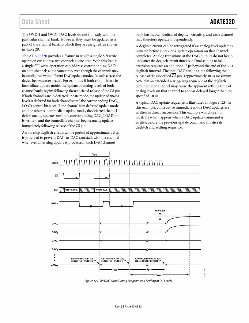
Data Sheet ADATE320
Rev. B | Page 53 of 82
The OVDH and OVDL DAC levels do not fit neatly within a particular channel bank. However, they must be updated as a part of the channel bank to which they are assigned, as shown in Table 29.
The ADATE320 provides a feature in which a single SPI write operation can address two channels at one time. With this feature, a single SPI write operation can address corresponding DACs on both channels at the same time, even though the channels may be configured with different DAC update modes. In such a case, the device behaves as expected. For example, if both channels are in immediate update mode, the update of analog levels of both channel banks begins following the associated release of the CS pin. If both channels are in deferred update mode, the update of analog levels is deferred for both channels until the corresponding DAC_ LOAD control bit is set. If one channel is in deferred update mode and the other is in immediate update mode, the deferred channel defers analog updates until the corresponding DAC_LOAD bit is written, and the immediate channel begins analog updates immediately following release of the CS pin.
An on-chip deglitch circuit with a period of approximately 3 µs is provided to prevent DAC-to-DAC crosstalk within a channel whenever an analog update is processed. Each DAC channel
bank has its own dedicated deglitch circuitry, and each channel may therefore operate independently.
A deglitch circuit can be retriggered if an analog level update is initiated before a previous update operation on that channel completes. Analog transitions at the DAC outputs do not begin until after the deglitch circuit times out. Final settling to full precision requires an additional 7 µs beyond the end of the 3 µs deglitch interval. The total DAC settling time following the release of the associated CS pin is approximately 10 µs maximum. Note that an extended retriggering sequence of the deglitch circuit on one channel may cause the apparent settling time of analog levels on that channel to appear delayed longer than the specified 10 µs.
A typical DAC update sequence is illustrated in Figure 129. In this example, consecutive immediate mode DAC updates are written in direct succession. This example was chosen to illustrate what happens when a DAC update command is written before the previous update command finishes its deglitch and settling sequence.
CS
BUSY
SCLK
tSPI
DAC2
DAC3
BEGINNING OF 3µsDEGLITCH PERIOD
RETRIGGER OF 3µsDEGLITCH PERIOD
COMPLETION OF 3µsDEGLITCH PERIOD
DAC15
SDI WRITE DAC1WRITE DAC0
DAC0
DAC1
±0.5 LSB
tSPI 3µs
tDAC 1216
0-02
6
Figure 129. SPI DAC Write Timing Diagram and Settling of DC Levels

ADATE320 Data Sheet
Rev. B | Page 54 of 82
DAC Levels and VTHERM Pin Transfer Function
Table 24. Detailed DAC Code to/from Voltage Level Transfer Functions
Level Programmable Range (0x0000 to 0xFFFF) DAC-to-Level and Level-to-DAC Transfer Functions
VILx, VIHx, VITx/VCOMx, VOLx, VOHx, POLx, POHx, VCHx, VCLx, PCHx, PCLx, OVDHx, OVDLx, PPMUx (FV), PCHx (FI), PCLx (FI)
−2.5 V to +7.5 V VDUTx = (4 × (DAC/216) − 1) × (VREF − VREFGND) + VDUTGND DAC = ((VDUTx − VDUTGND) + (VREF − VREFGND))/(4 × (VREF −VREFGND)) × 216
IOHx, IOLx −12.5 mA to +37.5 mA IDUTx = (4 × (DAC/216) − 1) × (VREF − VREFGND) × (25 mA/5) DAC = ((IDUTx × (5/25 mA)) + (VREF − VREFGND))/(4 × (VREF − VREFGND)) × 216
PPMUx (FI, Range A), PCHx and PCLx (FV, Range A)
−80 mA to +80 mA IDUTx = (4 × (DAC/216) − 2) × (VREF − VREFGND) × (80 mA/5) DAC = ((IDUTx/80 mA × 5) + 2 × (VREF − VREFGND))/(4 × (VREF − VREFGND)) × 216
PPMUx (FI, Range B), PCHx and PCLx (FV, Range B)
−2 mA to +2 mA IDUTx = (4 × (DAC/216) − 2) × (VREF − VREFGND) × (2 mA/5) DAC = ((IDUTx/2 mA × 5) + 2 × (VREF − VREFGND))/(4 × (VREF − VREFGND)) × 216
PPMUx (FI, Range C), PCHx and PCLx (FV, Range C)
−200 µA to +200 µA IDUTx = (4 × (DAC/216) − 2) × (VREF − VREFGND) × (200 µA/5) DAC = ((IDUTx/200 µA × 5) + 2 × (VREF − VREFGND))/(4 × (VREF − VREFGND)) × 216
PPMUx (FI, Range D) PCHx and PCLx (FV, Range D)
−20 µA to +20 µA IDUTx = (4 × (DAC/216) − 2) × (VREF − VREFGND) × (20 µA/5) DAC = ((IDUTx/20 µA × 5) + 2 × (VREF − VREFGND))/(4 × (VREF − VREFGND)) × 216
PPMUx (FI, Range E) PCHx and PCLx (FV, Range E)
−4 µA to +4 µA IDUTx = (4 × (DAC/216) − 2) × (VREF − VREFGND) × (4 µA/5) DAC = ((IDUTx/4 µA × 5) + 2 × (VREF − VREFGND))/(4 × (VREF − VREFGND)) × 216
Table 25. Load Transfer Functions Load Level Transfer Functions Notes IOLx VIOLx/(2 × (VREF − VREFGND)) × 25 mA VIOLx DAC levels are not referenced to VDUTGND IOHx VIOHx/(2 × (VREF − VREFGND)) × 25 mA VIOHx DAC levels are not referenced to VDUTGND
Table 26. PPMU Transfer Functions PPMU Mode Transfer Functions1 Uncalibrated PPMU DAC Settings to Achieve Specified PPMU Range FV VDUTx = PPMUx −1.5 V < PPMUx < +4.5 V FI IDUTx = (PPMUx − (VREF − VREFGND))/(5 × RPPMU) 0.0 V < PPMUx < 5.0 V MV VPPMU_Mx = VDUTx (internal sense path) Not applicable MV VPPMU_Mx = VPPMU_Sx (external sense path) Not applicable MI VPPMU_Mx = (VREF − VREFGND) + (5 × IDUTx × RPPMU) + VDUTGND Not applicable 1 RPPMU = 12.5 Ω for Range A, 500 Ω for Range B, 5.0 kΩ for Range C, 50 kΩ for Range D, and 250 kΩ for Range E.
Table 27. Temperature Sensor Transfer Function Temperature Output 0 K 0.00 V 300 K 3.00 V TKELVIN 0.00 V + (TKELVIN ) × 10 mV/K

Data Sheet ADATE320
Rev. B | Page 55 of 82
DAC Gain and Offset Correction
Each analog function within the ADATE320 has independent gain (m) and offset (c) calibration registers that allow digital trim of first-order errors in the analog signal chain. These registers correct errors in the pin electronics transfer functions as well as errors intrinsic to the DAC itself.
The m and c registers are volatile and must be reloaded after each power-on cycle as part of a calibration routine if values other than the defaults are required. The registers are not cleared by any reset operation (although the DAC_CAL_ENABLE bit is cleared following reset).
The gain and offset calibration function can be bypassed by clearing the DAC_CAL_ENABLE bit in the DAC control register (see Figure 146). This bypass mode is available only on a per chip basis. In other words, it is not possible to bypass the calibration function for a specific subset of the DACs.
The calibration function, when enabled, adjusts the numerical data sent to each DAC according to the following equation:
( )1516 2
21
−+
×
+
= cXm
X 12 (1)
where: X2 is the 16-bit data-word gated into the physical DAC, and returned by subsequent SPI read from that same DAC. m is the code in the respective DAC gain calibration register (the default code is 0xFFFF = 216 − 1). X1 is the 16-bit data-word written by the user to the DAC via the SPI. c is the code in the respective DAC offset calibration register (the default code is 0x8000 = 215).
From Equation 1, it can be seen that the gain applied to any written X1 data is always ≤1.0, with the effect that the effective output of a DAC can only be made smaller in magnitude by the calibration mechanism. To compensate for this imposed limitation, each of the analog signal paths in the pin electronics functions are guaranteed by designed to have a gain ≥1.0 when the default m register values are applied. A signal path gain ≥1.0 guarantees that proper gain calibration can always be achieved by multiplying down.
DAC X2 Registers and SPI Readback
When data is written via the SPI to a particular DAC, that data is operated on in accordance with Equation 1. The results are stored in an X2 register associated with that DAC (see Figure 130).
There is only a single physical X2 register per DAC, and it is the value of this X2 register that is eventually gated into the physical DAC at the time of analog update, which can be either in immedi-ate or deferred mode. It is also this register value that is returned to the user during an SPI read operation addressed to that DAC channel. In the special case of a dual channel write to a DAC, both of the associated X2 registers are sequentially updated using the appropriate m register and c register for each channel.
When enabled, the calibration function applies this operation to the X2 registers only after a SPI write to the respective X1 registers. The X2 registers are not updated after write operations to either m register or c register or following any changes to functional modes or range settings of the device. For this reason, to ensure that calibration data is recalculated for any particular DAC, it is necessary to write fresh data to that DAC after changes are first made to the associated m register and c register, and any associated functional modes and ranges for that DAC function.
For each DAC, there is only a single X2 register, and generally there is one dedicated and unique set of m calibration register and c calibration register assigned. In several special cases (for example, the PPMU DAC) there is still only one X2 register per DAC, but there are several different choices for m register and c register depending on the particular configuration of mode and range control settings for the function. For those DACs, a choice of calibration register is made automatically based on the respective mode and range control settings in place for that function when the DAC is written.
Table 28 describes detailed m register and c register selection as a function of mode and range control settings. For all DAC functions, it is necessary to ensure that the respective m register and c register values are put in place first, and that the desired mode and range settings are updated prior to sending data to the DAC. It is only during the DAC write sequence that the calibration constants are selected and applied.
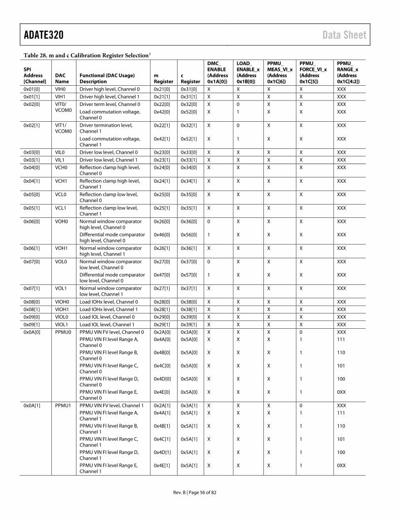
ADATE320 Data Sheet
Rev. B | Page 56 of 82
Table 28. m and c Calibration Register Selection1
SPI Address [Channel]
DAC Name
Functional (DAC Usage) Description
m Register
c Register
DMC_ ENABLE (Address 0x1A[0])
LOAD_ ENABLE_x (Address 0x1B[0])
PPMU_ MEAS_VI_x (Address 0x1C[6])
PPMU_ FORCE_VI_x (Address 0x1C[5])
PPMU_ RANGE_x (Address 0x1C[4:2])
0x01[0] VIH0 Driver high level, Channel 0 0x21[0] 0x31[0] X X X X XXX
0x01[1] VIH1 Driver high level, Channel 1 0x21[1] 0x31[1] X X X X XXX
0x02[0] VIT0/ VCOM0
Driver term level, Channel 0 0x22[0] 0x32[0] X 0 X X XXX
Load commutation voltage, Channel 0
0x42[0] 0x52[0] X 1 X X XXX
0x02[1] VIT1/ VCOM0
Driver termination level, Channel 1
0x22[1] 0x32[1] X 0 X X XXX
Load commutation voltage, Channel 1
0x42[1] 0x52[1] X 1 X X XXX
0x03[0] VIL0 Driver low level, Channel 0 0x23[0] 0x33[0] X X X X XXX
0x03[1] VIL1 Driver low level, Channel 1 0x23[1] 0x33[1] X X X X XXX
0x04[0] VCH0 Reflection clamp high level, Channel 0
0x24[0] 0x34[0] X X X X XXX
0x04[1] VCH1 Reflection clamp high level, Channel 1
0x24[1] 0x34[1] X X X X XXX
0x05[0] VCL0 Reflection clamp low level, Channel 0
0x25[0] 0x35[0] X X X X XXX
0x05[1] VCL1 Reflection clamp low level, Channel 1
0x25[1] 0x35[1] X X X X XXX
0x06[0] VOH0 Normal window comparator high level, Channel 0
0x26[0] 0x36[0] 0 X X X XXX
Differential mode comparator high level, Channel 0
0x46[0] 0x56[0] 1 X X X XXX
0x06[1] VOH1 Normal window comparator high level, Channel 1
0x26[1] 0x36[1] X X X X XXX
0x07[0] VOL0 Normal window comparator low level, Channel 0
0x27[0] 0x37[0] 0 X X X XXX
Differential mode comparator low level, Channel 0
0x47[0] 0x57[0] 1 X X X XXX
0x07[1] VOL1 Normal window comparator low level, Channel 1
0x27[1] 0x37[1] X X X X XXX
0x08[0] VIOH0 Load IOHx level, Channel 0 0x28[0] 0x38[0] X X X X XXX
0x08[1] VIOH1 Load IOHx level, Channel 1 0x28[1] 0x38[1] X X X X XXX
0x09[0] VIOL0 Load IOL level, Channel 0 0x29[0] 0x39[0] X X X X XXX
0x09[1] VIOL1 Load IOL level, Channel 1 0x29[1] 0x39[1] X X X X XXX
0x0A[0] PPMU0 PPMU VIN FV level, Channel 0 0x2A[0] 0x3A[0] X X X 0 XXX PPMU VIN FI level Range A,
Channel 0 0x4A[0] 0x5A[0] X X X 1 111
PPMU VIN FI level Range B, Channel 0
0x4B[0] 0x5A[0] X X X 1 110
PPMU VIN FI level Range C, Channel 0
0x4C[0] 0x5A[0] X X X 1 101
PPMU VIN FI level Range D, Channel 0
0x4D[0] 0x5A[0] X X X 1 100
PPMU VIN FI level Range E, Channel 0
0x4E[0] 0x5A[0] X X X 1 0XX
0x0A[1] PPMU1 PPMU VIN FV level, Channel 1 0x2A[1] 0x3A[1] X X X 0 XXX PPMU VIN FI level Range A,
Channel 1 0x4A[1] 0x5A[1] X X X 1 111
PPMU VIN FI level Range B, Channel 1
0x4B[1] 0x5A[1] X X X 1 110
PPMU VIN FI level Range C, Channel 1
0x4C[1] 0x5A[1] X X X 1 101
PPMU VIN FI level Range D, Channel 1
0x4D[1] 0x5A[1] X X X 1 100
PPMU VIN FI level Range E, Channel 1
0x4E[1] 0x5A[1] X X X 1 0XX

Data Sheet ADATE320
Rev. B | Page 57 of 82
SPI Address [Channel]
DAC Name
Functional (DAC Usage) Description
m Register
c Register
DMC_ ENABLE (Address 0x1A[0])
LOAD_ ENABLE_x (Address 0x1B[0])
PPMU_ MEAS_VI_x (Address 0x1C[6])
PPMU_ FORCE_VI_x (Address 0x1C[5])
PPMU_ RANGE_x (Address 0x1C[4:2])
0x0B[0] PCH0 PPMU current clamp (FV) high level, Channel 0
0x44[0] 0x54[0] X X X 0 XXX
PPMU voltage clamp (FI) high level, Channel 0
0x2B[0] 0x3B[0] 1
0x0B[1] PCH1 PPMU current clamp (FV) high level, Channel 1
0x44[1] 0x54[1] X X X 0 XXX
PPMU voltage clamp (FI) high level, Channel 1
0x2B[1] 0x3B[1] 1
0x0C[0] PCL0 PPMU current clamp (FV) low level, Channel 0
0x45[0] 0x55[0] X X X 0 XXX
PPMU voltage clamp (FI) low level, Channel 0
0x2C[0] 0x3C[0] 1
0x0C[1] PCL1 PPMU current clamp (FV) low level, Channel 1
0x45[1] 0x55[1] X X X 0 XXX
PPMU voltage clamp (FI) low level, Channel 1
0x2C[1] 0x3C[1] X X X 1
0x0D[0] POH0 PPMU go/no-go MV high level, Channel 0
0x2D[0] 0x3D[0] X X 0 X XXX
PPMU go/no-go MI Range A high level, Channel 0
0x61[0] 0x5D[0] X X 1 X 111
PPMU go/no-go MI Range B high level, Channel 0
0x62[0] 0x5D[0] X X 1 X 110
PPMU go/no-go MI Range C high level, Channel 0
0x63[0] 0x5D[0] X X 1 X 101
PPMU go/no-go MI Range D high level, Channel 0
0x64[0] 0x5D[0] X X 1 X 100
PPMU go/no-go MI Range E high level, Channel 0
0x65[0] 0x5D[0] X X 1 X 0XX
0x0D[1] POH1 PPMU go/no-go MV high level, Channel 1
0x2D[1] 0x3D[1] X X 0 X XXX
PPMU go/no-go MI Range A high level, Channel 1
0x61[1] 0x5D[1] X X 1 X 111
PPMU go/no-go MI Range B high level, Channel 1
0x62[1] 0x5D[1] X X 1 X 110
PPMU go/no-go MI Range C high level, Channel 1
0x63[1] 0x5D[1] X X 1 X 101
PPMU go/no-go MI Range D high level, Channel 1
0x641[] 0x5D[1] X X 1 X 100
PPMU go/no-go MI Range E high level, Channel 1
0x65[1] 0x5D[1 X X 1 X 0XX
0x0E[0] POL0 PPMU go/no-go MV low level, Channel 0
0x2E[0] 0x3E[0] X X 0 X XXX
PPMU go/no-go MI Range A low level, Channel 0
0x66[0] 0x5E[0] X X 1 X 111
PPMU go/no-go MI Range B low level, Channel 0
0x67[0] 0x5E[0] X X 1 X 110
PPMU go/no-go MI Range C low level, Channel 0
0x68[0] 0x5E[0] X X 1 X 101
PPMU go/no-go MI Range D low level, Channel 0
0x69[0] 0x5E[0] X X 1 X 100
PPMU go/no-go MI Range E low level, Channel 0
0x6A[0] 0x5E[0] X X 1 X 0XX

ADATE320 Data Sheet
Rev. B | Page 58 of 82
SPI Address [Channel]
DAC Name
Functional (DAC Usage) Description
m Register
c Register
DMC_ ENABLE (Address 0x1A[0])
LOAD_ ENABLE_x (Address 0x1B[0])
PPMU_ MEAS_VI_x (Address 0x1C[6])
PPMU_ FORCE_VI_x (Address 0x1C[5])
PPMU_ RANGE_x (Address 0x1C[4:2])
0x0E[1] POL1 PPMU go/no-go MV low level, Channel 1
0x2E[1] 0x3E[1] X X 0 X XXX
PPMU go/no-go MI Range A low level, Channel 1
0x66[1] 0x5E[1] X X 1 X 111
PPMU go/no-go MI Range B low level, Channel 1
0x67[1] 0x5E[1] X X 1 X 110
PPMU go/no-go MI Range C low level, Channel 1
0x68[1] 0x5E[1] X X 1 X 101
PPMU go/no-go MI Range D low level, Channel 1
0x69[1] 0x5E[1] X X 1 X 100
PPMU go/no-go MI Range E low level, Channel 1
0x6A[1] 0x5E[1] X X 1 X 0XX
0x0F[0] OVDL Overvoltage detect low level 0x2F[0] 0x3F[0] X X X X XXX
0x0F[1] OVDH Overvoltage detect high level 0x2F[1] 0x3F[1] X X X X XXX 1 X means don’t care.
M REGISTER C
EXAMPLE: VOL0 (ADDR: 0x07, CH0)DAC X1 REGISTER
M REGISTER BM REGISTER A
C REGISTER CC REGISTER B
C REGISTER A
PIN ELECTRONICS FUNCTIONALMODE AND RANGE SETTINGS
EXAMPLE: DMC_ENABLE (ADDR: 0x1A[0])
×
+
DAC X2 REGISTER
WRITEREAD
DAC_CAL_ENABLE (ADDR: 0x11[0])
DAC_LOAD (ADDR: 0x11[2])
DAC
SPI
01
ABC
ABC
DAC IMMEDIATEMODE ONE-SHOT
DAC_LOAD_MODE (ADDR: 0x11[1])
n × SCLKDELAY
1 = DEFERRED0 = IMMEDIATE
1216
0-02
7
Figure 130. DAC X2 Registers and Calibration Diagram
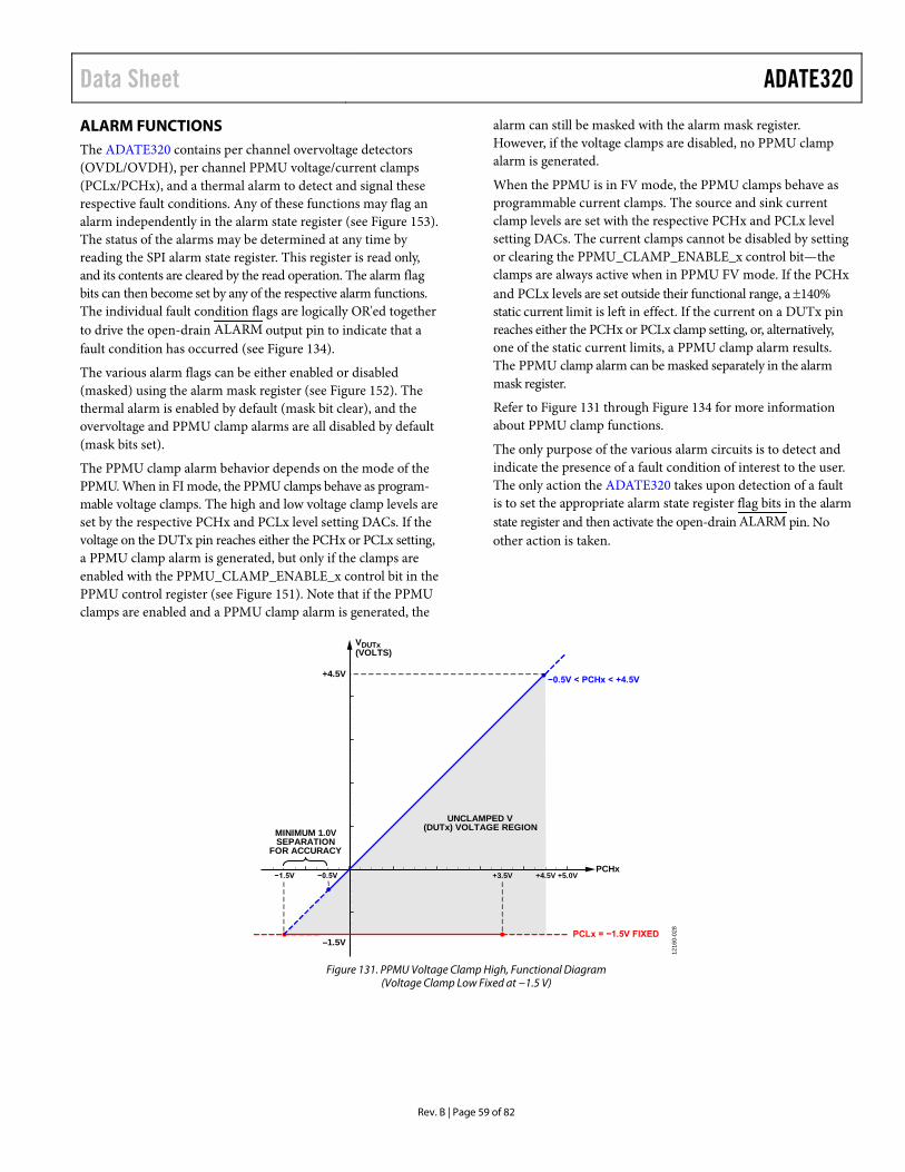
Data Sheet ADATE320
Rev. B | Page 59 of 82
ALARM FUNCTIONS The ADATE320 contains per channel overvoltage detectors (OVDL/OVDH), per channel PPMU voltage/current clamps (PCLx/PCHx), and a thermal alarm to detect and signal these respective fault conditions. Any of these functions may flag an alarm independently in the alarm state register (see Figure 153). The status of the alarms may be determined at any time by reading the SPI alarm state register. This register is read only, and its contents are cleared by the read operation. The alarm flag bits can then become set by any of the respective alarm functions. The individual fault condition flags are logically OR'ed together to drive the open-drain ALARM output pin to indicate that a fault condition has occurred (see Figure 134).
The various alarm flags can be either enabled or disabled (masked) using the alarm mask register (see Figure 152). The thermal alarm is enabled by default (mask bit clear), and the overvoltage and PPMU clamp alarms are all disabled by default (mask bits set).
The PPMU clamp alarm behavior depends on the mode of the PPMU. When in FI mode, the PPMU clamps behave as program-mable voltage clamps. The high and low voltage clamp levels are set by the respective PCHx and PCLx level setting DACs. If the voltage on the DUTx pin reaches either the PCHx or PCLx setting, a PPMU clamp alarm is generated, but only if the clamps are enabled with the PPMU_CLAMP_ENABLE_x control bit in the PPMU control register (see Figure 151). Note that if the PPMU clamps are enabled and a PPMU clamp alarm is generated, the
alarm can still be masked with the alarm mask register. However, if the voltage clamps are disabled, no PPMU clamp alarm is generated.
When the PPMU is in FV mode, the PPMU clamps behave as programmable current clamps. The source and sink current clamp levels are set with the respective PCHx and PCLx level setting DACs. The current clamps cannot be disabled by setting or clearing the PPMU_CLAMP_ENABLE_x control bit—the clamps are always active when in PPMU FV mode. If the PCHx and PCLx levels are set outside their functional range, a ±140% static current limit is left in effect. If the current on a DUTx pin reaches either the PCHx or PCLx clamp setting, or, alternatively, one of the static current limits, a PPMU clamp alarm results. The PPMU clamp alarm can be masked separately in the alarm mask register.
Refer to Figure 131 through Figure 134 for more information about PPMU clamp functions.
The only purpose of the various alarm circuits is to detect and indicate the presence of a fault condition of interest to the user. The only action the ADATE320 takes upon detection of a fault is to set the appropriate alarm state register flag bits in the alarm state register and then activate the open-drain ALARM pin. No other action is taken.
+4.5V
–1.5VPCLx = −1.5V FIXED
−0.5V < PCHx < +4.5V
PCHx
VDUTx(VOLTS)
UNCLAMPED V(DUTx) VOLTAGE REGION
−0.5V +3.5V +4.5V +5.0V−1.5V
MINIMUM 1.0VSEPARATION
FOR ACCURACY
1216
0-02
8
Figure 131. PPMU Voltage Clamp High, Functional Diagram
(Voltage Clamp Low Fixed at −1.5 V)

ADATE320 Data Sheet
Rev. B | Page 60 of 82
VDUTx(VOLTS)
+3.5V +4.5V
MINIMUM 1.0VSEPARATION
FOR ACCURACY
PCHx = +4.5V FIXED
PCLx
UNCLAMPED V(DUTx) VOLTAGE REGION −1.5V < PCLx < +3.5V
−0.5V−1.5V
1216
0-02
9
Figure 132. PPMU Voltage Clamp Low, Functional Diagram
(Voltage Clamp High Fixed at 4.5 V)
−1.0V +6.0V+2.0V +3.0V
−140% STATIC CURRENT LIMIT
−120%
−110%
−30%
−20%
+20%
+30%
+110%
+120%
+140% STATIC CURRENT LIMIT
FUNCTIONAL RANGE
DC ACCURACY RANGE
+5.5V−0.5V
+3.0V < PCHx < +5.5V
UNCLAMPED IDUTxPCHx CURRENT REGION
UNCLAMPED IDUTxPCLx CURRENT REGION
−0.5V < PCLx < +2.0V
PCHx/PCLxDAC SETTING
IDUTx(%FULL SCALE)
THE PCL CLAMP MUST BE < −20% FULL SCALE AND ALWAYS REMAIN INTHE LOWER (SINK) QUADRANT. THE PCH CLAMP MUST BE > +20% FULLSCALE AND ALWAYS REMAIN IN THE UPPER (SOURCE) QUADRANT.
ANY CURRENT CLAMP CONDITION (WHETHER PROGRAMMED OR ±140%STATIC CURRENT LIMIT) SETS THE PPMU CLAMP ALARM FLAGINDEPENDENT OF PPMU_CLAMP_ENABLE_x BIT IN THE PPMUCONTROL REGISTER.
1216
0-03
0
Figure 133. PPMU Current Clamp High and Low, Functional Diagram
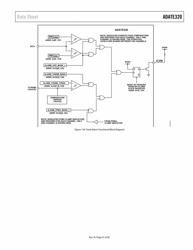
Data Sheet ADATE320
Rev. B | Page 61 of 82
VTHERM(10mV/K)
+
–
D Q
Q
DUTx
+
–
ADDR: 0x0F, CH0
DACOVDL
ADDR: 0x0F, CH1
DACOVDH
+
–
TEMPERATURESENSOR(10mV/K)
ADDR: 0x1D[2], CHx
ALARM_PPMU_MASK_x
ADDR: 0x1D[7:5], CH0
ALARM_THERM_THRES
ADDR: 0x1D[3], CH0
ALARM_THERM_MASK
ADDR: 0x1D[0], CHx
ALARM_OVD_MASK_x
FROM PPMUxCLAMP INDICATOR
RESET BY READINGFROM SPI ALARMSTATE REGISTERADDR: 0x1E, CHx
DVDD ALARM
DVDD
ADATE320
NOTE: DEDICATED OVERVOLTAGE COMPARATORSARE PROVIDED FOR EACH CHANNEL. ONLY ONECHANNEL IS SHOWN HERE. THE OVDH/OVDLLEVELS ARE SHARED BETWEEN THE CHANNELS.
NOTE: DEDICATED PPMU CLAMP INDICATORSARE PROVIDED FOR EACH CHANNEL. ONLYONE CHANNEL IS SHOWN HERE.
1216
0-03
1
Figure 134. Fault Alarm Functional Block Diagram

ADATE320 Data Sheet
Rev. B | Page 62 of 82
APPLICATIONS INFORMATION POWER SUPPLY, GROUNDING, AND TYPICAL DECOUPLING STRATEGY The ADATE320 is internally divided into a digital core and an analog core.
The VDD and DGND pins provide power and ground for the digital core that includes the SPI, certain logic functions, and the digital calibration functions. DGND is the logic ground reference for the VDD supply. Therefore, bypass VDD adequately to DGND with good quality, low effective series resistance (ESR) bypass capacitors. To reduce transient digital switching noise coupling to the analog core, connect DGND to a dedicated external ground plane that is separated from the analog ground domains. If the application permits, the DGND pins can share a digital ground domain with the supervisory FPGA or ASIC that interfaces with the ADATE320 SPI. All CMOS inputs and outputs are referenced between VDD and DGND, and their valid levels must be guaranteed relative to these power supply pins.
The analog core of the device includes all analog ATE functional blocks such as the DACs, the driver, the comparator, the load, and the PPMU. The VCC and VEE supplies provide power to the analog core. AGND and PGND are analog ground and power ground references, respectively. PGND is generally noisier with analog switching transients, and it may also have large static dc currents. AGND is generally quieter and has relatively smaller static dc currents. These two grounds can be connected together outside the chip to a single shared analog ground plane. Regardless, keep PGND and AGND (whether separated or shared) separated from the DGND ground plane if system design constraints permit.
The transient frequencies generated by the analog core can be a full order of magnitude greater than those generated by the SPI and on-chip digital circuitry. Therefore, pay close attention to the decoupling of the VCC and VEE supplies. Each supply must be adequately bypassed to the PGND ground domain using the highest quality bypass capacitors available. Locate the decoupling capacitors as close to the device as practically possible. The decoupling capacitors must have very low ESR and effective series inductance (ESL). Commonly available ceramic capacitors may provide only a marginally low impedance path to ground at the frequencies encountered in the ADATE320. Therefore, consider only the highest performance decoupling capacitors if
possible. In accordance with generally accepted practices, a typical 10 µF tantalum capacitor must also be shared across each power supply domain.
Pay particularly close attention to decoupling the VCC and VEE supplies in proximity to the transmission line at the DUTx pins of the device. To avoid undesired waveform aberrations and degradation of performance, it is important that all return currents to and from the transmission line have a direct and low impedance path back to the VCCDx and VEEDx pins adjacent to the respective DUTx pins. See Figure 135 for a typical transmission line decoupling strategy.
The ADATE320 has a DUTGND reference input pin that senses the remote low frequency ground potential at the target device under test (DUT). With the exception of the VIOH and VIOL active load currents and VPMU when in PPMU FI mode, all DAC levels are adjusted on-chip relative to this DUTGND input. Furthermore, the PPMU measure output pins (PPMU_Mx) are also referenced to DUTGND. The off-chip system analog-to-digital converter (ADC) that measures the PPMU_Mx pins must therefore be referenced to DUTGND as well. Referencing the system ADC to AGND results in errors unless DUTGND is tied directly to AGND as close as possible to the ADATE320. For applications that do not distinguish between DUT ground reference and system analog ground reference, the DUTGND pin may be connected to the same ground plane as AGND.
Avoid routing digital lines under the device, because these lines can couple noise into the device. Generous use of an analog ground plane under the device shields noise coupling that can otherwise enter the device. The power supply distribution lines must provide very wide and low inductance paths to the respective supply planes. This is especially true for VCC and VEE. Attention to via inductance is extremely important in these supplies—it cannot be neglected. Fast switching signals routed in proximity to the ADATE320 must be adequately shielded, preferably with their proper ground returns to avoid radiating noise to other parts of the board. Route such lines as far away as possible from the analog inputs to the device, such as the AGND, DUTGND, VREF, and VREFGND reference inputs.

Data Sheet ADATE320
Rev. B | Page 63 of 82
DUTxDRIVER
VCCDx
VEEDx
AGND
ANALOG POWER GROUND
DIGITAL POWER GROUND
20pF
10mA
CMPHx/CMPLx
CMPHx/CMPLx
VTTCx
COMP
SPI
VDD
DGND
DIGITAL +1.8V
SCLK
SDI
SDO
CS
ADATE320
DUTGND
DATx/RCVx
DATx/RCVx
VTTDxVTT TERMINATION
TO
AS
IC/F
PG
AT
O A
SIC
/FP
GA
PGND
VCC
VEE
ANALOG +8.0V
ANALOG –5.0V
VTT TERMINATION
DUT
BUSY
ALARM
DIGITAL 0.0V
ANALOG 0.0V
PGND
+8.0V
−5.0V
50Ω
50Ω
1216
0-03
2
Figure 135. Power Supply and Transmission Path Decoupling Detail

ADATE320 Data Sheet
Rev. B | Page 64 of 82
POWER SUPPLY SEQUENCING The ADATE320 is designed to tolerate sequencing of power supplies in any order. It is therefore not critical that the power supplies be sequenced in any particular order; however, there are recommended best practices.
The ADATE320 has two analog power supplies (VCC, VEE) and one digital power supply (VDD). The analog supplies service all of the analog functions on the chip such as level setting DACs, driver, comparator, load, and PPMU. The digital supply services the SPI and all digital CMOS control circuitry.
There is careful separation between the analog and digital partitions of the chip, and significant effort has been made to decouple these two partitions both functionally and electrically. The analog partition remains in the default configuration in the absence of VDD, and similarly, the digital partition remains in the default configuration in the absence of either (or both) VCC and VEE.
It is not possible to guarantee predictable behavior of the analog partition if either the VEE or VCC supply is poorly conditioned or absent. It is therefore recommended that any externally connected device be disconnected from the DUTx pin to prevent potential damage to that device while either of the VEE or VCC supplies is out of specification.
Assuming the VEE and VCC analog supplies are both applied and within specification, the analog partition ensures that all functions remain in the default configuration. This is true even when the VDD supply is absent and digital CMOS control circuitry is not yet functioning. In such a case (or whenever the RST pin is asserted), all of the level setting DACs takes the voltage present at the DUTGND input pin, and all SPI control bits assume their reset default values. The analog functions remain in this safe condition as long as VDD remains absent or as long as the RST pin remains asserted.
It is recommended that the RST pin always be asserted during the time that the VDD supply is being brought up. If this condition is met, the level setting DACs continue to hold the DUTGND potential after VDD stabilizes and after the RST pin is released. A fully clocked reset sequence then initializes the level setting DACs to the reset default conditions as specified in Table 29.
The reset sequence is described in more detail in the SPI Reset Sequence and the Pin section.
In light of these considerations, it is recommended that the two analog supplies be applied first. It is preferable that the smaller valued supply (VEE) be applied before the larger valued supply (VCC). Bring up the digital VDD supply next while the RST pin is asserted. After VDD is stable and the RST pin is subsequently released, a fully clocked reset sequence must follow. This power supply sequence ensures that analog functions and all level setting DACs receive the proper configuration information during the digital partition reset sequence.
The power supplies must be removed in the reverse order.
Note that VREF and the high speed transmission line termination pins (VTTDx, VTTCx) are all part of the analog partition, but they are not treated as supplies. VREF can be managed independent of VCC and VEE, provided its potential never goes outside those of the VEE and VCC supply buses to prevent ESD protection diodes from becoming forward biased. The VTTDx and VTTCx pins do not have this restriction relative to VCC and VEE, but they must never go outside the absolute maximum ratings as measured with respect to PGND.
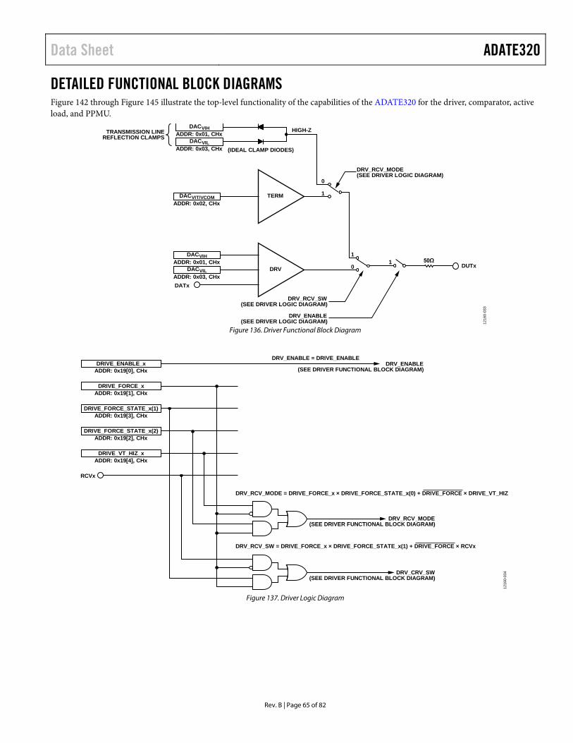
Data Sheet ADATE320
Rev. B | Page 65 of 82
DETAILED FUNCTIONAL BLOCK DIAGRAMS Figure 142 through Figure 145 illustrate the top-level functionality of the capabilities of the ADATE320 for the driver, comparator, active load, and PPMU.
DRV
DACVIHADDR: 0x01, CHx
DACVILADDR: 0x03, CHx
DACVIHADDR: 0x01, CHx
DACVILADDR: 0x03, CHx
TERMDACVIT/VCOMADDR: 0x02, CHx
50Ω
HIGH-Z
DATx
0
1
11 DUTx0
DRV_RCV_SW(SEE DRIVER LOGIC DIAGRAM)
DRV_RCV_MODE(SEE DRIVER LOGIC DIAGRAM)
DRV_ENABLE(SEE DRIVER LOGIC DIAGRAM)
(IDEAL CLAMP DIODES)
TRANSMISSION LINEREFLECTION CLAMPS
1216
0-03
3
Figure 136. Driver Functional Block Diagram
DRIVE_ENABLE_xADDR: 0x19[0], CHx
DRIVE_FORCE_xADDR: 0x19[1], CHx
DRIVE_FORCE_STATE_x(1)ADDR: 0x19[3], CHx
DRIVE_FORCE_STATE_x(2)ADDR: 0x19[2], CHx
DRIVE_VT_HIZ_xADDR: 0x19[4], CHx
RCVx
DRV_RCV_MODE(SEE DRIVER FUNCTIONAL BLOCK DIAGRAM)
DRV_ENABLE(SEE DRIVER FUNCTIONAL BLOCK DIAGRAM)
DRV_RCV_MODE = DRIVE_FORCE_x × DRIVE_FORCE_STATE_x(0) + DRIVE_FORCE × DRIVE_VT_HIZ
DRV_ENABLE = DRIVE_ENABLE
DRV_CRV_SW(SEE DRIVER FUNCTIONAL BLOCK DIAGRAM)
DRV_RCV_SW = DRIVE_FORCE_x × DRIVE_FORCE_STATE_x(1) + DRIVE_FORCE × RCVx
1216
0-03
4
Figure 137. Driver Logic Diagram
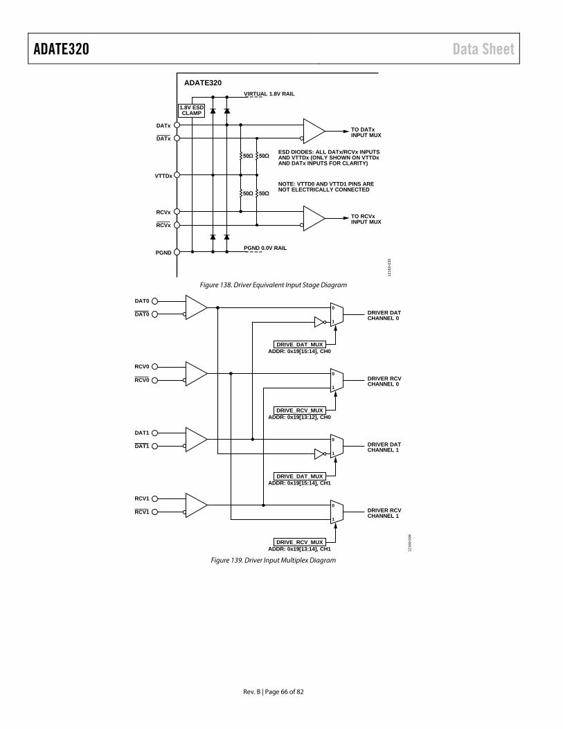
ADATE320 Data Sheet
Rev. B | Page 66 of 82
DATxTO DATxINPUT MUX
TO RCVxINPUT MUX
ESD DIODES: ALL DATx/RCVx INPUTSAND VTTDx (ONLY SHOWN ON VTTDxAND DATx INPUTS FOR CLARITY)
NOTE: VTTD0 AND VTTD1 PINS ARENOT ELECTRICALLY CONNECTED
DATx
RCVx
VTTDx
RCVx
PGNDPGND 0.0V RAIL
VIRTUAL 1.8V RAIL
1.8V ESDCLAMP
50Ω 50Ω
50Ω 50Ω
ADATE320
1216
0-03
5
Figure 138. Driver Equivalent Input Stage Diagram
0
1
DRIVE_DAT_MUXADDR: 0x19[15:14], CH0
DRIVER DATCHANNEL 0
0
1
DRIVE_RCV_MUXADDR: 0x19[13:12], CH0
DRIVER RCVCHANNEL 0
0
1
DRIVE_DAT_MUXADDR: 0x19[15:14], CH1
DRIVER DATCHANNEL 1
0
1
DRIVE_RCV_MUXADDR: 0x19[13:14], CH1
DRIVER RCVCHANNEL 1
DAT0
DAT0
RCV0
RCV0
DAT1
DAT1
RCV1
RCV1
1216
0-03
6
Figure 139. Driver Input Multiplex Diagram

Data Sheet ADATE320
Rev. B | Page 67 of 82
DACVOHADDR: 0x06, CH0
DACVOLADDR: 0x07, CH0
DMC_ENABLEADDR: 0x1A[0], CH0
DACVOH
TO DUT1
DUT0
A = 1
DACVOL
0
1
0
1
CMPH0CMPH0
CMPL0
DIFFERENTIALCOMPARATOR ONCHANNEL 0 ONLY
CMPL0
1216
0-03
7
Figure 140. Comparator Functional Block Diagram
50Ω 50Ω50Ω50Ω
1.8V ESDCLAMP
EXTERNALTERMINATION
50Ω
VTTCx
CMPx
CMPx
PGNDPGND 0.0V RAIL
ESD DIODES: ALL CMPH/LxOUTPUTS AND VTTCx (ONLYSHOWN ON VTTCx AND CMPHxOUTPUT FOR CLARITY)
≥200mV(TYPICAL = 250mV)
NOTE: VTTC0 AND VTTC1 PINSARE NOT ELECTRICALLYCONNECTED
VIRTUAL 1.8V RAIL
10mA
50Ω
ADATE320
1216
0-03
8
Figure 141. Comparator Equivalent Output Stage Diagram

ADATE320 Data Sheet
Rev. B | Page 68 of 82
50Ω
POWERCONTROL
DACVIT/VCOMADDR: 0x02, CHx
DACVIOHADDR: 0x08, CHx
DACVIOLADDR: 0x09, CHx
LOAD_POWER_DOWN(SEE LOAD LOGIC DIAGRAM)
ACTIVE LOAD
FROM DRIVER DUTx
LOAD_CONNECT(SEE LOAD LOGIC DIAGRAM)
1216
0-03
9
Figure 142. Active Load Functional Block Diagram
LOAD_ENABLE_xADDR: 0x1B[0], CHx
LOAD_FORCE_xADDR: 0x1B[1], CHx
DRIVE_VT_HIZ_xADDR: 0x19[4], CHx
RCVx
LOAD_CONNECT(SEE ACTIVE LOAD FUNCTIONAL BLOCK DIAGRAM)
LOAD_PWR_DOWN(SEE ACTIVE LOAD FUNCTIONAL BLOCK DIAGRAM)
LOAD_PWR_DOWN = LOAD_ENABLE_x
LOAD_CONNECT = LOAD_ENABLE_x × (RCVx × DRIVE_VT_HIZ_x + LOAD_FORCE_x)
1216
0-04
0
Figure 143. Active Load Functional Logic Diagram
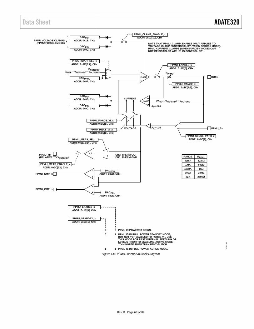
Data Sheet ADATE320
Rev. B | Page 69 of 82
DACPCHADDR: 0x1B, CHx
PPMU_CLAMP_ENABLE_xADDR: 0x1C[10], CHx
PPMU_RANGE_xADDR: 0x1C[4:2], CHx
PPMU_SENSE_PATH_xADDR: 0x1C[9], CHx
DACPCLADDR: 0x0C, CHx
PPMU_INPUT_SEL_xADDR: 0x1C[8:7], CHx
DACPPMUADDR: 0x0A, CHx
DACPCHADDR: 0x0B, CHx
DACPCLADDR: 0x0C, CHx
VOUTGND
(VREF – VREFGND) + VOUTGND
RPPMU
NOTE THAT PPMU_CLAMP_ENABLE ONLY APPLIES TOVOLTAGE CLAMP FUNCTIONALITY (WHEN FORCE-I MODE).PPMU CURRENT CLAMPS (WHEN FORCE-V MODE) CANNOT BE DISABLED WITH THIS CONTROL BIT.
CURRENT
VOLTAGE
CH0: THERM OUTCH0: THERM GND
AV = 5.0
AV = 1.0
(VREF – VREFGND) + VOUTGND
PPMU_FORCE_VI_xADDR: 0x1C[5], CHx
PPMU_MEAS_VI_xADDR: 0x1C[6], CHx
PPMU_MEAS_SELADDR: 0x1[15:14], CHx
PPMU_MEAS_ENABLE_xADDR: 0x1C[13], CHx
PPMU_ENABLE_xADDR: 0x1C[0], CHx
PPMU_STANDBY_xADDR: 0x1C[1], CHx
DACPOHADDR: 0x0D, CHx
DACPOLADDR: 0x0E, CHx
PPMU_ENABLE_xADDR: 0x1C[0], CHx
F-AMP
I-AMP
0
3
1
0
1
2DUTx
PPMU_Mx(RELATIVE TO VDUTGND)
PPMU_CMPHx
X 0 PPMU IS POWERED DOWN.PPMU IS IN FULL POWER STANDBY MODE,BUT NOT YET ENABLED TO FORCE V/I. USETHIS MODE FOR FAST INTERNAL SETTLING OFLEVELS PRIOR TO ENABLING ACTIVE MODETO MINIMIZE PPMU TRANSIENT GLITCH.
PPMU IS IN FULL POWER ACTIVE MODE.
0 1
1 1
PPMU_CMPHx
PPMU_Sx
×1RANGE40mA1mA
100µA10µA2µA
RPPMU12.5Ω500Ω5kΩ
20kΩ250kΩ
PPMU VOLTAGE CLAMPS(PPMU FORCE-I MODE)
1216
0-04
1
Figure 144. PPMU Functional Block Diagram

ADATE320 Data Sheet
Rev. B | Page 70 of 82
PPMU_MEAS_SEL_xADDR: 0x1C[15:14], CHx
DACPOHADDR: 0x0D, CHx
DACPOLADDR: 0x0E, CHx
PPMU_MEAS_ENABLE_xADDR: 0x1C[13], CHx
1×1
0
CH0: THERM OUTCH0: THERM GND
FROM PPMU CIRCUIT
VOHx
VOLx
PPMU_Mx
PPMU_CMPHx
PPMU_CMPLx
PPMU GO/NO-GOCOMPARATORDC DAC LEVELS
PPMU_Mx
PPMU_CMPHx
PPMU_CMPLx
CONDITIONPPMU GO/NO-GO COMPARATOR TRUTH TABLE
PINPPMU_Mx < VOHx
PPMU_CMPHx
PPMU_CMPLx
PPMU_Mx < VOHxPPMU_Mx < VOLxPPMU_Mx < VOLx
STATELOWHIGHLOWHIGH
1216
0-04
2
Figure 145. PPMU Go/No-Go Comparator Functional Block Diagram
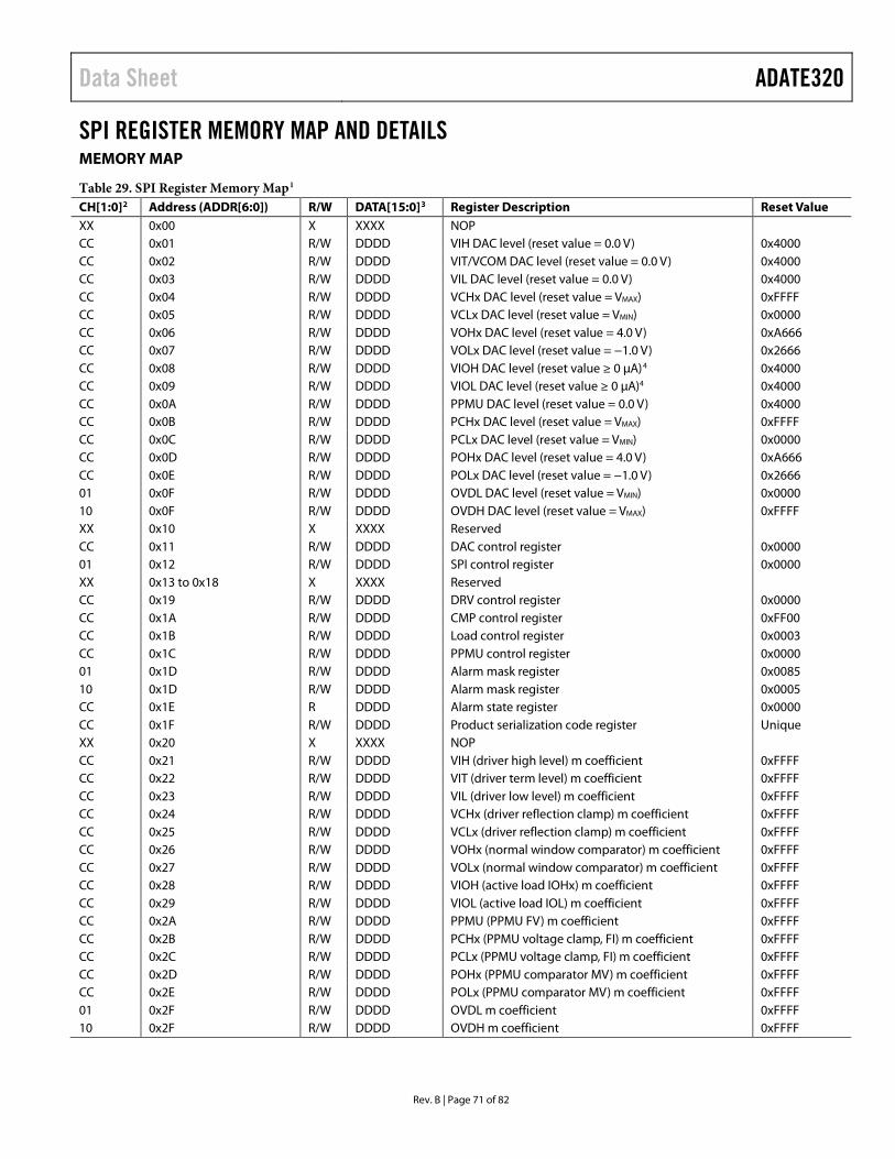
Data Sheet ADATE320
Rev. B | Page 71 of 82
SPI REGISTER MEMORY MAP AND DETAILS MEMORY MAP
Table 29. SPI Register Memory Map1 CH[1:0]2 Address (ADDR[6:0]) R/W DATA[15:0]3 Register Description Reset Value XX 0x00 X XXXX NOP CC 0x01 R/W DDDD VIH DAC level (reset value = 0.0 V) 0x4000 CC 0x02 R/W DDDD VIT/VCOM DAC level (reset value = 0.0 V) 0x4000 CC 0x03 R/W DDDD VIL DAC level (reset value = 0.0 V) 0x4000 CC 0x04 R/W DDDD VCHx DAC level (reset value = VMAX) 0xFFFF CC 0x05 R/W DDDD VCLx DAC level (reset value = VMIN) 0x0000 CC 0x06 R/W DDDD VOHx DAC level (reset value = 4.0 V) 0xA666 CC 0x07 R/W DDDD VOLx DAC level (reset value = −1.0 V) 0x2666 CC 0x08 R/W DDDD VIOH DAC level (reset value ≥ 0 µA)4 0x4000 CC 0x09 R/W DDDD VIOL DAC level (reset value ≥ 0 µA)4 0x4000 CC 0x0A R/W DDDD PPMU DAC level (reset value = 0.0 V) 0x4000 CC 0x0B R/W DDDD PCHx DAC level (reset value = VMAX) 0xFFFF CC 0x0C R/W DDDD PCLx DAC level (reset value = VMIN) 0x0000 CC 0x0D R/W DDDD POHx DAC level (reset value = 4.0 V) 0xA666 CC 0x0E R/W DDDD POLx DAC level (reset value = −1.0 V) 0x2666 01 0x0F R/W DDDD OVDL DAC level (reset value = VMIN) 0x0000 10 0x0F R/W DDDD OVDH DAC level (reset value = VMAX) 0xFFFF XX 0x10 X XXXX Reserved CC 0x11 R/W DDDD DAC control register 0x0000 01 0x12 R/W DDDD SPI control register 0x0000 XX 0x13 to 0x18 X XXXX Reserved CC 0x19 R/W DDDD DRV control register 0x0000 CC 0x1A R/W DDDD CMP control register 0xFF00 CC 0x1B R/W DDDD Load control register 0x0003 CC 0x1C R/W DDDD PPMU control register 0x0000 01 0x1D R/W DDDD Alarm mask register 0x0085 10 0x1D R/W DDDD Alarm mask register 0x0005 CC 0x1E R DDDD Alarm state register 0x0000 CC 0x1F R/W DDDD Product serialization code register Unique XX 0x20 X XXXX NOP CC 0x21 R/W DDDD VIH (driver high level) m coefficient 0xFFFF CC 0x22 R/W DDDD VIT (driver term level) m coefficient 0xFFFF CC 0x23 R/W DDDD VIL (driver low level) m coefficient 0xFFFF CC 0x24 R/W DDDD VCHx (driver reflection clamp) m coefficient 0xFFFF CC 0x25 R/W DDDD VCLx (driver reflection clamp) m coefficient 0xFFFF CC 0x26 R/W DDDD VOHx (normal window comparator) m coefficient 0xFFFF CC 0x27 R/W DDDD VOLx (normal window comparator) m coefficient 0xFFFF CC 0x28 R/W DDDD VIOH (active load IOHx) m coefficient 0xFFFF CC 0x29 R/W DDDD VIOL (active load IOL) m coefficient 0xFFFF CC 0x2A R/W DDDD PPMU (PPMU FV) m coefficient 0xFFFF CC 0x2B R/W DDDD PCHx (PPMU voltage clamp, FI) m coefficient 0xFFFF CC 0x2C R/W DDDD PCLx (PPMU voltage clamp, FI) m coefficient 0xFFFF CC 0x2D R/W DDDD POHx (PPMU comparator MV) m coefficient 0xFFFF CC 0x2E R/W DDDD POLx (PPMU comparator MV) m coefficient 0xFFFF 01 0x2F R/W DDDD OVDL m coefficient 0xFFFF 10 0x2F R/W DDDD OVDH m coefficient 0xFFFF

ADATE320 Data Sheet
Rev. B | Page 72 of 82
CH[1:0]2 Address (ADDR[6:0]) R/W DATA[15:0]3 Register Description Reset Value XX 0x30 X XXXX Reserved CC 0x31 R/W DDDD VIH (driver high level) c coefficient 0x8000 CC 0x32 R/W DDDD VIT (driver term level) c coefficient 0x8000 CC 0x33 R/W DDDD VIL (driver low level) c coefficient 0x8000 CC 0x34 R/W DDDD VCHx (driver reflection clamp) c coefficient 0x8000 CC 0x35 R/W DDDD VCLx (driver reflection clamp) c coefficient 0x8000 CC 0x36 R/W DDDD VOHx (normal window comparator) c coefficient 0x8000 CC 0x37 R/W DDDD VOLx (normal window comparator) c coefficient 0x8000 CC 0x38 R/W DDDD VIOH (active load IOHx) c coefficient 0x8000 CC 0x39 R/W DDDD VIOL (active load IOL) c coefficient 0x8000 CC 0x3A R/W DDDD PPMU (PPMU FV) c coefficient 0x8000 CC 0x3B R/W DDDD PCHx (PPMU voltage clamp, FI) c coefficient 0x8000 CC 0x3C R/W DDDD PCLx (PPMU voltage clamp, FI) c coefficient 0x8000 CC 0x3D R/W DDDD POHx (PPMU comparator MV) c coefficient 0x8000 CC 0x3E R/W DDDD POLx (PPMU comparator MV) c coefficient 0x8000 01 0x3F R/W DDDD OVDL c coefficient 0x8000 10 0x3F R/W DDDD OVDH c coefficient 0x8000 XX 0x40 to 0x41 X XXXX Reserved CC 0x42 R/W DDDD VCOM (active load) m coefficient 0xFFFF XX 0x43 X XXXX Reserved CC 0x44 R/W DDDD PCHx (PPMU current clamp, FV) m coefficient 0xFFFF CC 0x45 R/W DDDD PCLx (PPMU current clamp, FV) m coefficient 0xFFFF 01 0x46 R/W DDDD VOHx (differential comparator) m coefficient 0xFFFF 01 0x47 R/W DDDD VOLx (differential comparator) m coefficient 0xFFFF XX 0x48 to 0x49 X XXXX Reserved CC 0x4A R/W DDDD PPMU FI Range A m coefficient 0xFFFF CC 0x4B R/W DDDD PPMU FI Range B m coefficient 0xFFFF CC 0x4C R/W DDDD PPMU FI Range C m coefficient 0xFFFF CC 0x4D R/W DDDD PPMU FI Range D m coefficient 0xFFFF CC 0x4E R/W DDDD PPMU FI Range E m coefficient 0xFFFF XX 0x4F X XXXX Reserved XX 0x50 to 0x51 X XXXX Reserved CC 0x52 R/W DDDD VCOM (active load) c coefficient 0x8000 XX 0x53 X XXXX Reserved CC 0x54 R/W DDDD PCHx (PPMU current clamp, FV) c coefficient 0x8000 CC 0x55 R/W DDDD PCLx (PPMU current clamp, FV) c coefficient 0x8000 01 0x56 R/W DDDD VOHx (differential comparator) c coefficient 0x8000 01 0x57 R/W DDDD VOLx (differential comparator) c coefficient 0x8000 XX 0x58 to 0x59 X XXXX Reserved CC 0x5A R/W DDDD PPMU FI c coefficient 0x8000 XX 0x5B to 0x5C X XXXX Reserved CC 0x5D R/W DDDD POHx (PPMU comparator MI) c coefficient 0x8000 CC 0x5E R/W DDDD POLx (PPMU comparator MI) c coefficient 0x8000 XX 0x5F X XXXX Reserved XX 0x60 X XXXX Reserved CC 0x61 R/W DDDD POHx (PPMU comparator MI Range A) m coefficient 0xFFFF CC 0x62 R/W DDDD POHx (PPMU comparator MI Range B) m coefficient 0xFFFF CC 0x63 R/W DDDD POHx (PPMU comparator MI Range C) m coefficient 0xFFFF CC 0x64 R/W DDDD POHx (PPMU comparator MI Range D) m coefficient 0xFFFF CC 0x65 R/W DDDD POHx (PPMU comparator MI Range E) m coefficient 0xFFFF CC 0x66 R/W DDDD POLx (PPMU comparator MI Range A) m coefficient 0xFFFF

Data Sheet ADATE320
Rev. B | Page 73 of 82
CH[1:0]2 Address (ADDR[6:0]) R/W DATA[15:0]3 Register Description Reset Value CC 0x67 R/W DDDD POLx (PPMU comparator MI Range B) m coefficient 0xFFFF CC 0x68 R/W DDDD POLx (PPMU comparator MI Range C) m coefficient 0xFFFF CC 0x69 R/W DDDD POLx (PPMU comparator MI Range D) m coefficient 0xFFFF CC 0x6A R/W DDDD POLx (PPMU comparator MI Range E) m coefficient 0xFFFF XX 0x6B to 0x7F X XXXX Reserved 1 X means don’t care for the respective field. 2 CC represents two contiguous binary channel bits. 3 DDDD represents four-digit hexadecimal data. 4 The active load VIOHx and VIOLx voltage offsets are guaranteed to be nonzero and positive. These offsets result in a nonzero current for each IOHx and IOLx level
following valid reset sequence and prior to calibration. Furthermore, the active load is forced into the active on state following a reset, which facilitates a soft connect of the DUTx pin to VCOMx = 0.0 V following a valid reset sequence (with small but nonzero IOHx and IOLx currents).

ADATE320 Data Sheet
Rev. B | Page 74 of 82
REGISTER DETAILS Reserved bits in any register are undefined. In some cases, a physical but unused memory bit may be present.
Any SPI read operation from a reserved bit or register results in an unknown but deterministic readback value. Any SPI write operation to a reserved bit or register results in no action.
A write to a control bit or control register defined only on Channel 0 must be addressed to Channel 0. Any such write that
is addressed to only Channel 1 is ignored if no register or control bit is defined on Channel 1.
Furthermore, any such write that is addressed to both Channel 0 and Channel 1 (as a multichannel write) proceeds as if the write is addressed to both Channel 0 and Channel 1. If no register or control bit is defined at Channel 1, data addressed to the undefined Channel 1 is ignored. If a register or control bit is defined at Channel 1, it is filled as part of the multichannel write.
RESERVED
DAC LOAD CONTROL BIT, SELF RESETTING, CHANNEL 0/CHANNEL 1[0] = DEFAULT STATE OF THE DAC_LOAD CONTROL BIT1 = BEGIN DAC LOAD OPERATION (PULSE, SELF CLEAR TO ZERO)A WRITE TO THIS BIT PARALLEL UPDATES ALL DACs OF CHANNEL xWITH PREVIOUSLY BUFFERED DATA ASSUMING THAT THEDAC_LOAD_MODE CONTROL BIT OF CHANNEL x IS NOT SET TOWRITE DAC IMMEDIATE MODE. THIS BIT AUTOMATICALLY SELF CLEARS.
D1 D0D15 D14 D13 D12 D11 D10 D9 D8 D7 D6 D5 D4 D3 D2
24 2510 11 12 13 14 15 16 17 18 19 20 21 22 23
DATA-WORD INDEX
SPI CLOCK INDEX
DAC CALIBRATION ENGINE ENABLE, CHANNEL 0 ONLY[0] = CALIBRATION ENGINE IS DISABLED1 = CALIBRATION ENGINE IS ENABLEDWHEN DAC CALIBRATION IS ENABLED, EACH WRITE TO A VALID DACADDRESS RESULTS IN A SUBSEQUENT MULTIPLY AND ACCUMULATE(MAC) OPERATION TO THE DATA FOR THE RESPECTIVE DAC USINGCALIBRATION DATA CONTAINED IN THE APPROPRIATE m AND cCOEFFICIENT REGISTERS. WHEN THE CALIBRATION ENGINE ISDISABLED, DATA WRITTEN TO A VALID DAC ADDRESS IS NOTMODIFIED BY THE ON-CHIP CALIBRATION COEFFICIENTS.
DAC LOAD MODE, CHANNEL 0/CHANNEL 1[0] = WRITE DAC IMMEDIATE MODE.1 = WRITE DAC DEFERRED MODE.IN WRITE DAC IMMEDIATE MODE, EACH RESPECTIVE DAC IS UPDATEDIMMEDIATELY SUBSEQUENT TO A VALID SPI WRITE INSTRUCTION TOTHAT DAC ADDRESS. IN WRITE DAC DEFERRED MODE, EACH VALIDSPI WRITE TO A DAC ADDRESS IS BUFFERED, AND DACs ARE ONLYUPDATED FOLLOWING ASSERTION OF THE DAC_LOAD SOFT PIN.IN THIS MODE, ALL ANALOG DAC DATA FOR EITHER OR BOTHCHANNELS CAN BE UPDATED IN PARALLEL.
1216
0-01
7
Figure 146. DAC Control Register (Address 0x11)
RESERVED
SPI SOFTWARE RESET, CHANNEL 0 ONLY[0] = DEFAULT SETTING, NO ACTION IS TAKEN UNTIL A 1 IS WRITTEN.1 = RESET (PULSE, SELF CLEAR TO ZERO).FOLLOWING A WRITE TO SET THIS BIT, A FULL RESET SEQUENCE ISINITIATED THAT IS SIMILAR TO THE RST PIN ASSERTING ASYNCHRONOUSLY.FOLLOWING A RESET, THIS BIT SELF CLEARS TO THE DEFAULT 0 CONDITION.
D1 D0D15 D14 D13 D12 D11 D10 D9 D8 D7 D6 D5 D4 D3 D2
24 2510 11 12 13 14 15 16 17 18 19 20 21 22 23
DATA-WORD INDEX
SPI CLOCK INDEX
SPI SERIAL DATA OUTPUT PIN, HIGH-Z CONTROL, CHANNEL 0 ONLY[0] = SDO PIN IS ALWAYS ACTIVE, INDEPENDENT OF THE CS INPUT.1 = SDO PIN IS ACTIVE ONLY WHEN CS IS ACTIVE, OTHERWISE HIGH-Z.
1216
0-01
8
Figure 147. SPI Control Register (Address 0x12)

Data Sheet ADATE320
Rev. B | Page 75 of 82
DRIVER DAT INPUT MULTIPLEX SELECT,CHANNEL 0/CHANNEL 1[X0] = PRIMARY CHANNEL DATx, NO INVERTX1 = SECONDARY CHANNEL DATx, INVERTED
RESERVED
DRIVER VT/HIZ MODE SELECT, CHANNEL 0/CHANNEL 1[0] = DRIVER GOES TO HIGH-Z STATE WHEN RCVx = 11 = DRIVER GOES TO VIT STATE WHEN RCVx = 1WHEN DRIVE_VT_HIZ_x IS ASSERTED, THE DRIVER ON CHANNEL x ASSUMESTHE VIT LEVEL ON ASSERTION OF THE RCVx HIGH SPEED INPUT IN ACCORDANCE WITHTHE DRIVER TRUTH TABLE. THIS CONTROL BIT IS SUBORDINATE TO THE DRIVE_ENABLE_xAND DRIVE_FORCE_x CONTROL BITS.
DRIVER STATE WHEN DRIVE_FORCE, CHANNEL 0/CHANNEL 1[00] = FORCE DRIVE VIL STATE01 = FORCE DRIVE VIH STATE10 = FORCE DRIVE HIGH-Z STATE11 = FORCE DRIVE VIT STATEWHEN THE DRIVE_FORCE_x CONTROL BIT IS ACTIVE, THEN THE DRIVER ON CHANNEL xASSUMES THE INDICATED STATE IN ACCORDANCE WITH THE DRIVER TRUTH TABLE.
FORCE DRIVER TO DRIVE_FORCE_STATE, CHANNEL 0/CHANNEL 1[0] = DRIVER RESPONDS TO DATx AND RCVx1 = FORCE DRIVER STATE TO DRIVE_FORCE_STATEWHEN DRIVE_FORCE_x IS ASSERTED, THE DRIVER ON CHANNEL x ASSUMES THESTATE INDICATED BY DRIVE_FORCE_STATE_x IN ACCORDANCE WITH DRIVER TRUTH TABLE.THIS CONTROL BIT IS SUBORDINATE TO THE DRIVE_ENABLE_x CONTROL BIT, BUT TAKESPRECEDENCE OVER THE DRIVE_VT_HIZ_x BIT AS WELL AS THE DATx AND RCVx HIGH SPEEDINPUTS. THIS BIT DOES NOT FORCE THE SELECTION OF DRIVER LEVEL CALIBRATION CONSTANTS.
DRIVER ENABLE, CHANNEL 0/CHANNEL 1[0] = DRIVER IS DISABLED AND IN LOW LEAKAGE POWER DOWN MODE1 = DRIVER IS ENABLED AND RESPONDS TO DRIVE_VT_HIZ_x, DATx, AND RCVxWHEN DRIVE_ENABLE_x IS ASSERTED, THE DRIVER ON CHANNEL X ISENABLED RESPONDS TO BOTH THE DRIVE_FORCE_x AND DRIVE_VT_HIZ_xCONTROL BITS AS WELL AS THE RCVx AND DATx HIGH SPEED INPUTS IN ACCORDANCEWITH THE DRIVER TRUTH TABLE.
DRIVER RCV INPUT MULTIPLEX SELECT,CHANNEL 0/CHANNEL 1[X0] = PRIMARY CHANNEL RCVx, NO INVERTX1 = SECONDARY CHANNEL RCVx, NO INVERT
DRIVER CABLE LOSS COMPENSATION, CHANNEL 0/CHANNEL 1[000] = DISABLE DRIVER CLC001 = ENABLE DRIVER MINIMUM CLC111 = ENABLE DRIVER MAXIMUM CLCWHEN SET TO 000 THE DRIVER ON CHANNEL x HAS ZERO CABLE LOSSCOMPENSATION (CLC) ADDED TO ITS OUTPUT CHARACTERISTICS. WHEN SET TOA VALUE OTHER THAN 000, CLC PRE-EMPHASIS IS ADDED AND THE PERCENTAGEVALUE IS CONTROLLED BY THIS REGISTER VALUE.
D1 D0D15 D14 D13 D12 D11 D10 D9 D8 D7 D6 D5 D4 D3 D2
24 2510 11 12 13 14 15 16 17 18 19 20 21 22 23
DATA-WORD INDEX
SPI CLOCK INDEX
1216
0-01
9
Figure 148. DRV Control Register (Address 0x19)
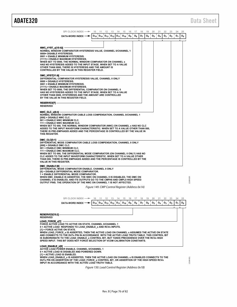
ADATE320 Data Sheet
Rev. B | Page 76 of 82
NORMAL WINDOW COMPARATOR HYSTERESIS VALUE, CHANNEL 0/CHANNEL 10000= DISABLE HYSTERESIS.0001 = ENABLE MINIMUM HYSTERESIS.[1111] = ENABLE MAXIMUM HYSTERESIS.WHEN SET TO 0000, THE NORMAL WINDOW COMPARATOR ON CHANNEL xHAS NO HYSTERESIS ADDED TO THE INPUT STAGE. WHEN SET TO A VALUEOTHER THAN 0000, THERE IS HYSTERESIS AND THE AMOUNT ISCONTROLLED BY THE VALUE IN THIS REGISTER FIELD.
DIFFERENTIAL COMPARATOR HYSTERESIS VALUE, CHANNEL 0 ONLY0000 = DISABLE HYSTERESIS.0001 = ENABLE MINIMUM HYSTERESIS.[1111] = ENABLE MAXIMUM HYSTERESIS.WHEN SET TO 0000, THE DIFFERENTIAL COMPARATOR ON CHANNEL 0HAS NO HYSTERESIS ADDED TO THE INPUT STAGE. WHEN SET TO A VALUEOTHER THAN 0000, HYSTERESIS AND THE AMOUNT ARE CONTROLLEDBY THE VALUE IN THIS REGISTER FIELD.
RESERVED
D1 D0D15 D14 D13 D12 D11 D10 D9 D8 D7 D6 D5 D4 D3 D2
24 2510 11 12 13 14 15 16 17 18 19 20 21 22 23
DATA-WORD INDEX
SPI CLOCK INDEX
NORMAL WINDOW COMPRATOR CABLE LOSS COMPENSATION, CHANNEL 0/CHANNEL 1[000] = DISABLE NWC CLC.001 = ENABLE NWC MINIMUM CLC.111 = ENABLE NWC MAXIMUM CLC.WHEN SET TO 000, THE NORMAL WINDOW COMPARATOR (NWC) ON CHANNEL x HAS NO CLCADDED TO THE INPUT WAVEFORM CHARACTERISTIC. WHEN SET TO A VALUE OTHER THAN 000,THERE IS PRE-EMPHASIS ADDED AND THE PERCENTAGE IS CONTROLLED BY THE VALUE INTHIS REGISTER.
DIFFERENTIAL MODE COMPARATOR CABLE LOSS COMPENSATION, CHANNEL 0 ONLY[000] = DISABLE DMC CLC.001 = ENABLE DMC MINIMUM CLC.111 = ENABLE DMC MAXIMUM CLC.WHEN SET TO 000, THE DIFFERENTIAL MODE COMPARATOR (ON CHANNEL 0 ONLY) HAS NOCLC ADDED TO THE INPUT WAVEFORM CHARACTERISTIC. WHEN SET TO A VALUE OTHERTHAN 000, THERE IS PRE-EMPHASIS ADDED AND THE PERCENTAGE IS CONTROLLED BY THEVALUE IN THIS REGISTER.
DIFFERENTIAL MODE COMPARATOR ENABLE, CHANNEL 0 ONLY[0] = DISABLE DIFFERENTIAL MODE COMPARATOR.1 = ENABLE DIFFERENTIAL MODE COMPARATOR.WHEN DMC_ENABLE IS ASSERTED, THE NWC ON CHANNEL 0 IS DISABLED, THE DMC ONCHANNEL 0 IS ENABLED, AND ITS OUTPUTS GO TO THE CMPH0 AND CMPL0 HIGH SPEEDOUTPUT PINS. THE OPERATION OF THE NWC ON CHANNEL 1 IS NOT AFFECTED. 12
160-
020
Figure 149. CMP Control Register (Address 0x1A)
D1 D0D15 D14 D13 D12 D11 D10 D9 D8 D7 D6 D5 D4 D3 D2
24 2510 11 12 13 14 15 16 17 18 19 20 21 22 23
DATA-WORD INDEX
SPI CLOCK INDEX
RESERVED
FORCE ACTIVE LOAD TO ACTIVE ON STATE, CHANNEL 0/CHANNEL 10 = ACTIVE LOAD RESPONDS TO LOAD_ENABLE_x AND RCVx INPUTS.[1] = FORCE ACTIVE ON STATE.WHEN LOAD_FORCE_x IS ASSERTED, THEN THE ACTIVE LOAD ON CHANNEL x ASSUMES THE ACTIVE ON STATEAND CONNECTS TO THE DUTx PIN IN ACCORDANCE WITH THE ACTIVE LOAD TRUTH TABLE. THIS CONTROL BITIS SUBORDINATE TO THE LOAD_ENABLE_x CONTROL BIT, BUT TAKES PRECEDENCE OVER THE RCVx HIGHSPEED INPUT. THIS BIT DOES NOT FORCE SELECTION OF VCOM CALIBRATION CONSTANTS.
ACTIVE LOAD POWER ENABLE, CHANNEL 0/CHANNEL 10 = ACTIVE LOAD IS DISABLED AND POWERED DOWN.[1] = ACTIVE LOAD IS ENABLED.WHEN LOAD_ENABLE_x IS ASSERTED, THEN THE ACTIVE LOAD ON CHANNEL x IS ENABLED CONNECTS TO THEDUTx PIN ON ASSERTION OF THE LOAD_FORCE_x CONTROL BIT, OR ASSERTION OF THE HIGH SPEED RCVxINPUT IN ACCORDANCE WITH THE ACTIVE LOAD TRUTH TABLE. 12
160-
021
Figure 150. Load Control Register (Address 0x1B)

Data Sheet ADATE320
Rev. B | Page 77 of 82
D1 D0D15 D14 D13 D12 D11 D10 D9 D8 D7 D6 D5 D4 D3 D2
24 2510 11 12 13 14 15 16 17 18 19 20 21 22 23
DATA-WORD INDEX
SPI CLOCK INDEX
PPMU ANALOG MEASURE OUT PIN SELECT, CHANNEL 0/CHANNEL 1[X0] = PPMU CHANNEL x TO PPMU_MEASx OUTPUT PINX1 = CHANNEL 0: TEMPERATURE SENSOR OUTPUT (VTHERM)CHANNEL 1: TEMPERATURE SENSOR GROUND REFERENCE
PPMU ANALOG MEASURE OUT PIN ENABLE, CHANNEL 0/CHANNEL 1[0] = PPMU MEASURE OUT PIN ON CHANNEL x IS HIGH-Z1 = PPMU MEASURE OUT PIN ON CHANNEL x IS ENABLED
PPMU VOLTAGE CLAMP ENABLE, CHANNEL 0/CHANNEL 1[0] = PPMU VOLTAGE CLAMPS DISABLED1 = PPMU VOLTAGE CLAMPS ENABLEDAPPLIES ONLY TO VOLTAGE CLAMPS WHEN IN FORCE-I MODE.PROGRAMMABLE CURRENT CLAMPS CANNOT BE DISABLED.
PPMU SENSE PATH, CHANNEL 0/CHANNEL 1[0] = PPMU INTERNAL SENSE PATH1 = PPMU EXTERNAL SENSE PATH
PPMU INPUT SELECT, CHANNEL 0/CHANNEL 1[00] = PPMU INPUT FROM DUTGND01 = PPMU INPUT FROM DUTGND + 2.5V1X = PPMU INPUT FROM DACPPMU LEVEL
PPMU MV OR MI, CHANNEL 0/CHANNEL 1[0] = PPMU MV MODE1 = PPMU MI MODE
PPMU FV OR FI, CHANNEL 0/CHANNEL 1[0] = PPMU FV MODE1 = PPMU FI MODE
PPMU RANGE, CHANNEL 0/CHANNEL 1[0XX] = PPMU RANGE E (2µA)100 = PPMU RANGE D (10µA)101 = PPMU RANGE C (100µA)110 = PPMU RANGE B (1mA)111 = PPMU RANGE A (40mA)
PPMU STANDBY, CHANNEL 0/CHANNEL 1[0] = PPMU FULL POWER ACTIVE1 = PPMU FULL POWER STANDBY
PPMU POWER ENABLE, CHANNEL 0/CHANNEL 1[0] = PPMU LOW POWER OFF1 = PPMU FULL POWER ON
RESERVED
1216
0-02
2
Figure 151. PPMU Control Register (Address 0x1C)
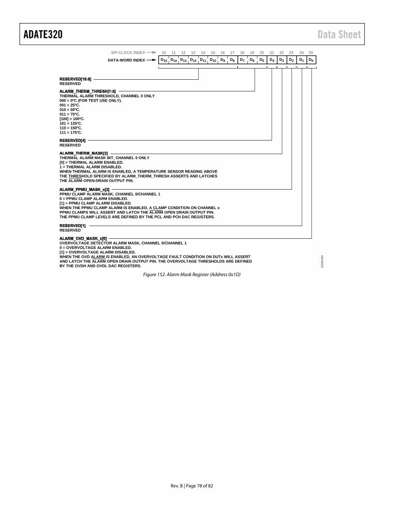
ADATE320 Data Sheet
Rev. B | Page 78 of 82
D1 D0D15 D14 D13 D12 D11 D10 D9 D8 D7 D6 D5 D4 D3 D2
24 2510 11 12 13 14 15 16 17 18 19 20 21 22 23
DATA-WORD INDEX
SPI CLOCK INDEX
RESERVED
RESERVED
RESERVED
THERMAL ALARM MASK BIT, CHANNEL 0 ONLY[0] = THERMAL ALARM ENABLED.1 = THERMAL ALARM DISABLED.WHEN THERMAL ALARM IS ENABLED, A TEMPERATURE SENSOR READING ABOVETHE THRESHOLD SPECIFIED BY ALARM_THERM_THRESH ASSERTS AND LATCHESTHE ALARM OPEN-DRAIN OUTPUT PIN.
PPMU CLAMP ALARM MASK, CHANNEL 0/CHANNEL 10 = PPMU CLAMP ALARM ENABLED.[1] = PPMU CLAMP ALARM DISABLED.WHEN THE PPMU CLAMP ALARM IS ENABLED, A CLAMP CONDITION ON CHANNEL xPPMU CLAMPS WILL ASSERT AND LATCH THE ALARM OPEN DRAIN OUTPUT PIN.THE PPMU CLAMP LEVELS ARE DEFINED BY THE PCL AND PCH DAC REGISTERS.
OVERVOLTAGE DETECTOR ALARM MASK, CHANNEL 0/CHANNEL 10 = OVERVOLTAGE ALARM ENABLED.[1] = OVERVOLTAGE ALARM DISABLED.WHEN THE OVD ALARM IS ENABLED, AN OVERVOLTAGE FAULT CONDITION ON DUTx WILL ASSERTAND LATCH THE ALARM OPEN DRAIN OUTPUT PIN. THE OVERVOLTAGE THRESHOLDS ARE DEFINEDBY THE OVDH AND OVDL DAC REGISTERS.
THERMAL ALARM THRESHOLD, CHANNEL 0 ONLY000 = 0ºC (FOR TEST USE ONLY).001 = 25ºC.010 = 50ºC.011 = 75ºC.[100] = 100ºC.101 = 125ºC.110 = 150ºC.111 = 175ºC.
1216
0-02
3
Figure 152. Alarm Mask Register (Address 0x1D)

Data Sheet ADATE320
Rev. B | Page 79 of 82
D1 D0D15 D14 D13 D12 D11 D10 D9 D8 D7 D6 D5 D4 D3 D2
24 2510 11 12 13 14 15 16 17 18 19 20 21 22 23
DATA-WORD INDEX
SPI CLOCK INDEX
RESERVED
THERMAL ALARM FLAG, CHANNEL 0 ONLY[0] = THERMAL FAULT NOT DETECTED.1 = THERMAL FAULT DETECTED.WHEN THE ALARM_THERM_FLAG BIT IS SET, A FAULT WAS DETECTED ON THE DIE ACCORDING TOTHE THERMAL THRESHOLD SET IN THE ALARM_THERM_THRESH BIT. THIS FLAG IS SUBORDINATETO THE ALARM_THERM_MASK CONTROL BIT, AND IT AUTOMATICALLY RESETS AFTER ANY READFROM THE ALARM STATE REGISTER.
PPMU ALARM FLAG, CHANNEL 0/CHANNEL 1[0] = PPMU VOLTAGE/CURRENT CLAMP OR STATIC CURRENT LIMIT CONDITION NOT DETECTED.1 = PPMU VOLTAGE/CURRENT CLAMP OR STATIC CURRENT LIMIT CONDITION DETECTED.WHEN THE ALARM_PPMU_FLAG_x BIT IS SET, THEN A PPMU VOLTAGE/CURRENT CLAMP OR STATICCURRENT LIMIT CONDITION IS DETECTED ON CHANNEL x. THIS FLAG IS SUBORDINATE TO THEALARM_PPMU_MASK_x CONTROL BIT, AND AUTOMATICALLY RESETS AFTER ANY READ FROM THE ALARMSTATE REGISTER.
OVERVOLTAGE ALARM FLAG, CHANNEL 0/CHANNEL 1[0] = OVERVOLTAGE FAULT NOT DETECTED.1 = OVERVOLTAGE FAULT DETECTED.WHEN ALARM_OVDH_FLAG IS SET, AN OVERVOLTAGE FAULT CONDITION IS DETECTED ON CHANNEL xDUTx PIN ACCORDING TO THE THRESHOLD SET IN THE OVDH DAC REGISTER. THIS FLAG IS SUBORDINATETO THE ALARM_OVD_MASK_x CONTROL BIT, AND IT AUTOMATICALLY RESETS AFTER ANY READ FROMTHE ALARM STATE REGISTER.
UNDERVOLTAGE ALARM FLAG, CHANNEL 0/CHANNEL 1[0] = UNDERVOLTAGE FAULT NOT DETECTED.1 = UNDERVOLTAGE FAULT DETECTED.WHEN ALARM_OVDL_FLAG_x IS SET, AN UNDERVOLTAGE FAULT CONDITION IS DETECTED ON CHANNEL xDUTx PIN ACCORDING TO THE THRESHOLD SET IN THE OVDL DAC REGISTER. THIS FLAG IS SUBORDINATETO THE ALARM_OVD_MASK_x CONTROL BIT, AND AUTOMATICALLY RESETS AFTER ANY READ FROM THEALARM STATE REGISTER. 12
160-
024
Figure 153. Alarm State Register (Address 0x1E) (Read Only)
D1 D0D15 D14 D13 D12 D11 D10 D9 D8 D7 D6 D5 D4 D3 D2
24 2510 11 12 13 14 15 16 17 18 19 20 21 22 23
DATA-WORD INDEX
SPI CLOCK INDEX
PRODUCT SERIALIZATION CODE REGISTER, CHANNEL 0/CHANNEL 1THIS REGISTER CONTAINS UNIQUE NONVOLATILE PRODUCT IDENTIFICATION INFORMATION THAT ISWRITTEN TO THE DEVICE DURING MANUFACTURE. THIS REGISTER IS INITIALIZED DURING RESET TOTHE DATA TRIMMED INTO NONVOLATILE FUSE MEMORY. WHILE IT IS POSSIBLE TO WRITE SOMETEMPORARY DATA TO THIS REGISTER, IT HAS NO EFFECT ON OPERATION OF THE DEVICE. THECONTENTS OF THE REGISTER ARE REINITIALIZED AT NEXT RESET TO THE FACTORY PROGRAMMEDVALUES. THERE ARE 32 BITS OF IDENTIFICATION DATA CONTAINED IN THIS REGISTER, AS FOLLOWS:
CHAN 0: PRODUCT SERIALIZATION CODE LOW (LOWER HALF) CHAN 1: PRODUCT SERIALIZATION CODE HIGH (UPPER HALF)
1216
0-02
5
Figure 154. Product Serialization Code Register (Address 0x1F)
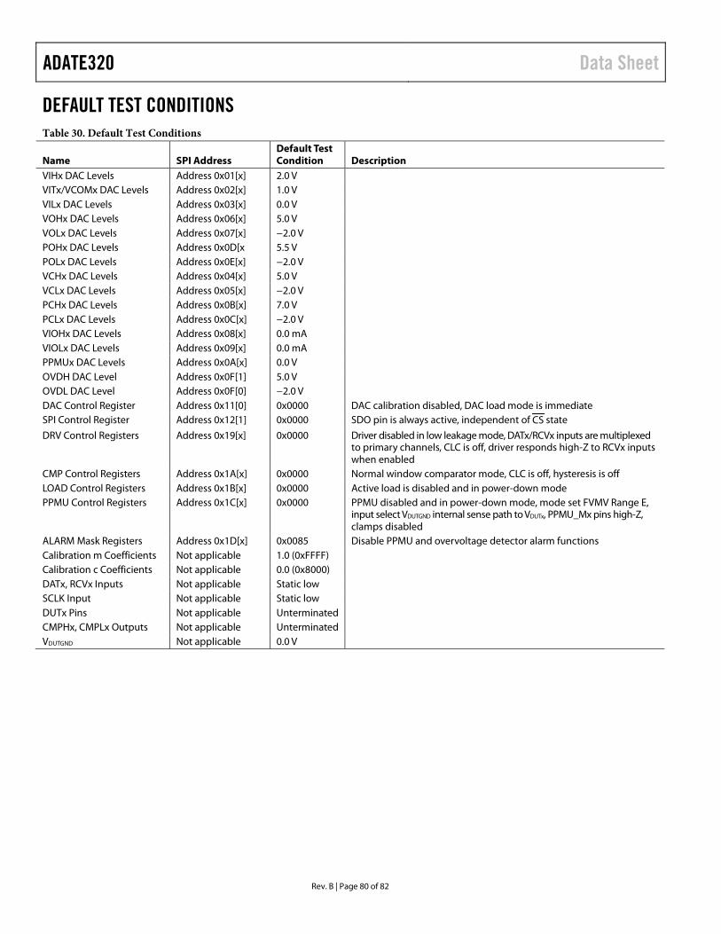
ADATE320 Data Sheet
Rev. B | Page 80 of 82
DEFAULT TEST CONDITIONS Table 30. Default Test Conditions
Name SPI Address Default Test Condition Description
VIHx DAC Levels Address 0x01[x] 2.0 V VITx/VCOMx DAC Levels Address 0x02[x] 1.0 V VILx DAC Levels Address 0x03[x] 0.0 V VOHx DAC Levels Address 0x06[x] 5.0 V VOLx DAC Levels Address 0x07[x] −2.0 V POHx DAC Levels Address 0x0D[x 5.5 V POLx DAC Levels Address 0x0E[x] −2.0 V VCHx DAC Levels Address 0x04[x] 5.0 V VCLx DAC Levels Address 0x05[x] −2.0 V PCHx DAC Levels Address 0x0B[x] 7.0 V PCLx DAC Levels Address 0x0C[x] −2.0 V VIOHx DAC Levels Address 0x08[x] 0.0 mA VIOLx DAC Levels Address 0x09[x] 0.0 mA PPMUx DAC Levels Address 0x0A[x] 0.0 V OVDH DAC Level Address 0x0F[1] 5.0 V OVDL DAC Level Address 0x0F[0] −2.0 V DAC Control Register Address 0x11[0] 0x0000 DAC calibration disabled, DAC load mode is immediate SPI Control Register Address 0x12[1] 0x0000 SDO pin is always active, independent of CS state
DRV Control Registers Address 0x19[x] 0x0000 Driver disabled in low leakage mode, DATx/RCVx inputs are multiplexed to primary channels, CLC is off, driver responds high-Z to RCVx inputs when enabled
CMP Control Registers Address 0x1A[x] 0x0000 Normal window comparator mode, CLC is off, hysteresis is off LOAD Control Registers Address 0x1B[x] 0x0000 Active load is disabled and in power-down mode PPMU Control Registers Address 0x1C[x] 0x0000 PPMU disabled and in power-down mode, mode set FVMV Range E,
input select VDUTGND internal sense path to VDUTx, PPMU_Mx pins high-Z, clamps disabled
ALARM Mask Registers Address 0x1D[x] 0x0085 Disable PPMU and overvoltage detector alarm functions Calibration m Coefficients Not applicable 1.0 (0xFFFF) Calibration c Coefficients Not applicable 0.0 (0x8000) DATx, RCVx Inputs Not applicable Static low SCLK Input Not applicable Static low DUTx Pins Not applicable Unterminated CMPHx, CMPLx Outputs Not applicable Unterminated VDUTGND Not applicable 0.0 V
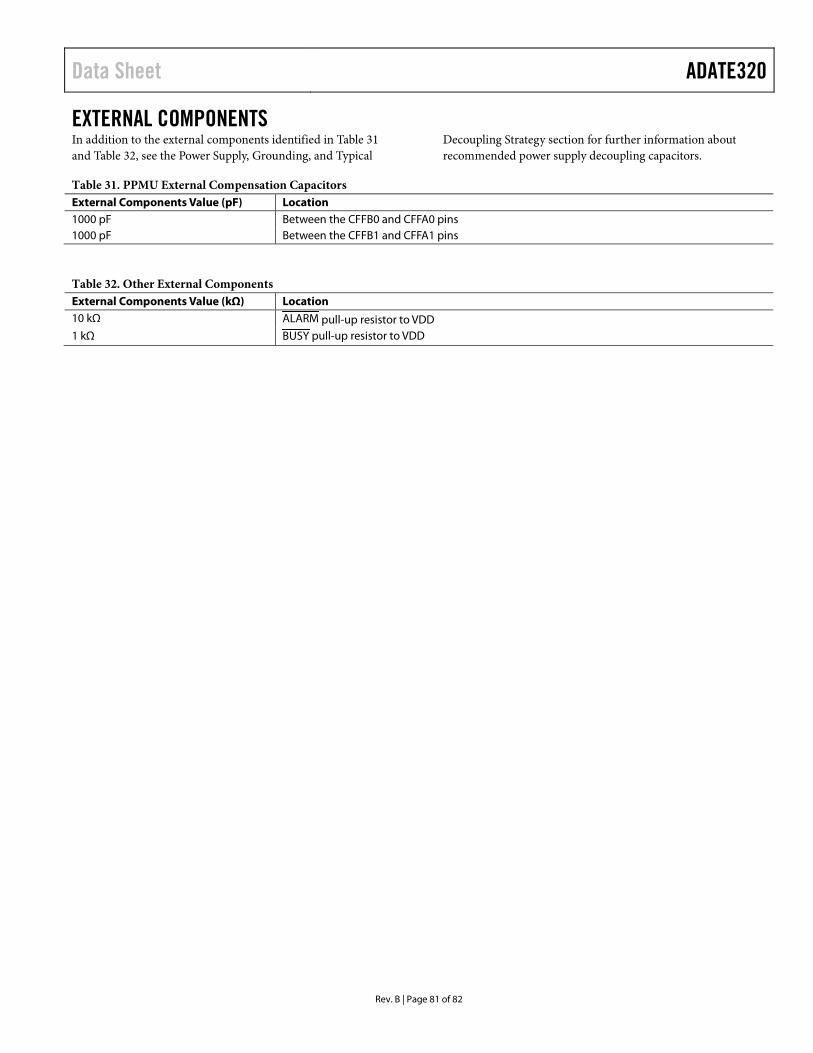
Data Sheet ADATE320
Rev. B | Page 81 of 82
EXTERNAL COMPONENTS In addition to the external components identified in Table 31 and Table 32, see the Power Supply, Grounding, and Typical
Decoupling Strategy section for further information about recommended power supply decoupling capacitors.
Table 31. PPMU External Compensation Capacitors External Components Value (pF) Location 1000 pF Between the CFFB0 and CFFA0 pins 1000 pF Between the CFFB1 and CFFA1 pins
Table 32. Other External Components External Components Value (kΩ) Location 10 kΩ ALARM pull-up resistor to VDD 1 kΩ BUSY pull-up resistor to VDD
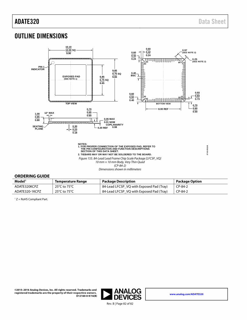
ADATE320 Data Sheet
Rev. B | Page 82 of 82
OUTLINE DIMENSIONS
1
21
63
43 2242
8464
0.600.500.40
0.600.420.24
0.600.420.24
0.300.230.18
8.00 REF
6.856.75 SQ6.65
0.40BSC
0.20 REF
12° MAX
0.05 MAX0.01 NOM
SEATINGPLANE
0.700.600.50
TOP VIEW
PIN 1INDICATOR
1.000.850.80
0.700.650.60
BOTTOM VIEW
NOTES:1. FOR PROPER CONNECTION OF THE EXPOSED PAD, REFER TO
THE PIN CONFIGURATION AND FUNCTION DESCRIPTIONSSECTION OF THIS DATA SHEET.
2. TIEBARS MAY OR MAY NOT BE SOLDERED TO THE BOARD. 07-0
2-20
12-B
0.930.830.73
0.97(SEE NOTE 2)
0.25(SEE NOTE 2)
EXPOSED PAD(SEE NOTE 1)
10.1010.00 SQ9.90
9.859.75 SQ9.65
COPLANARITY0.08
Figure 155. 84-Lead Lead Frame Chip Scale Package [LFCSP_VQ]
10 mm × 10 mm Body, Very Thin Quad (CP-84-2)
Dimensions shown in millimeters
ORDERING GUIDE Model1 Temperature Range Package Description Package Option ADATE320KCPZ 25°C to 75°C 84-Lead LFCSP_VQ with Exposed Pad (Tray) CP-84-2 ADATE320-1KCPZ 25°C to 75°C 84-Lead LFCSP_VQ with Exposed Pad (Tray) CP-84-2 1 Z = RoHS Compliant Part.
©2015–2016 Analog Devices, Inc. All rights reserved. Trademarks and registered trademarks are the property of their respective owners.
D12160-0-9/16(B)
www.analog.com/ADATE320