Embed Size (px)
Citation preview

1212 IEEE JOURNAL OF SOLID-STATE CIRCUITS, VOL. 40, NO. 6, JUNE 2005
Device Mismatch and Tradeoffs in the Designof Analog CircuitsPeter R. Kinget, Senior Member, IEEE
Abstract—Random device mismatch plays an important role inthe design of accurate analog circuits. Models for the matching ofMOS and bipolar devices from open literature show that matchingimproves with increasing device area. As a result, accuracy re-quirements impose a minimal device area and this paper exploresthe impact of this constraint on the performance of general analogcircuits. It results in a fixed bandwidth-accuracy-power tradeoffwhich is set by technology constants. This tradeoff is independentof bias point for bipolar circuits whereas for MOS circuits somebias point optimizations are possible. The performance limita-tions imposed by matching are compared to the limits imposedby thermal noise. For MOS circuits the power constraints dueto matching are several orders of magnitude higher than forthermal noise. For the bipolar case the constraints due to noiseand matching are of comparable order of magnitude. The impactof technology scaling on the conclusions of this work are brieflyexplored.
Index Terms—BiCMOS analog integrated circuits, bipolaranalog integrated circuits, bipolar transistors, circuit analysis,CMOS analog integrated circuits, design methodology, mismatch,matching, MOSFETs, sensitivity.
I. INTRODUCTION
DEVICE mismatch is too often treated as part of theblack art of analog design. However, extensive studies
into the matching behavior of devices have yielded a goodunderstanding of the underlying physical phenomena and offerdesigners quantitative models for the prediction of device vari-ations. Section II of this paper reviews the mismatch data andmodels published in open literature, which show that a circuitdesigner can improve the matching of devices by increasingtheir area. In Section III the effects of device mismatches onthe dc operation of basic transistor configurations are analyzed.Traditionally such analysis is done on the basis of large signaldevice equations and, for larger circuits, results in tediouscalculations or requires many simplifying assumptions. Weillustrate an analysis method for the calculation of the dc accu-racy of large analog circuits based on a small signal analysis.
Several authors have discussed the challenges and systemlevel limitations in analog signal processing imposed by thermalnoise and device mismatch (see, e.g., [1]–[4]). The main goalof this paper is to investigate in detail the impact of transistormismatch on the design tradeoffs at the circuit level. The yieldof offset sensitive analog circuits such as some analog-to-digitalconverters [5], digital-to-analog converters [6], and analog com-putation circuits [7], depends on the accuracy of the sub-blocks;
Manuscript received September 21, 2004; revised February 22, 2005.The author is with the Department of Electrical Engineering, Columbia Uni-
versity, New York, NY 10027 USA (e-mail: [email protected]).Digital Object Identifier 10.1109/JSSC.2005.848021
from the desired parametric yield for the overall circuit optimalaccuracy specifications are derived which together with the re-quired bandwidth and low power consumption are importantrequirements during the design. In Section IV we demonstratethat, since the accuracy specifications impose a minimal devicearea, they fix the tradeoff between power and bandwidth forbasic analog building blocks such as, current mirrors, invertingvoltage amplifiers and operational transconductance amplifiers.For MOS circuits the tradeoff can be slightly improved with theoptimization of the bias point and the optimization of voltageand current signal processing circuits is analyzed in detail. How-ever, the bandwidth-accuracy-power tradeoff is largely fixed anddetermined by technological parameters.
The tradeoff relationships derived for the circuit level are thenextended to evaluate the limitations of analog signal processingin Section V. The mismatch limits on power consumption arecompared to the thermal noise limits. The evolution of theselimits with process scaling is also discussed. Finally, we brieflyreview some techniques that can break the mismatch imposedlimits in certain applications.
The link between accuracy requirements, the speed or band-width and the power consumption applies to analog circuits fora wide range of applications such as bandgaps [8], [9], RAMsense amplifier design [10], high-speed analog-to-digital con-verters [7], [11], [12] and digital-to-analog converters [6], par-allel analog pre-processing and computation chips [13], [14],and sensor arrays and read-out electronics as in, e.g., high-en-ergy physics experiments [15] or CMOS imagers.
II. EXPERIMENTAL DATA FOR DEVICE MISMATCH
Manufacturing variations result in process and device pa-rameter variations from lot to lot, wafer to wafer, die to die,and device to device and can be categorized as systematic orrandom. Lot-to-lot and wafer-to-wafer variations are commonto all devices in the circuit. E.g., due to over-etching all tran-sistors have a shorter than nominal length. They introduce asystematic shift in the device characteristics and circuit per-formance. Differential circuit topologies and proper biasingtechniques can make the integrated circuit’s performancelargely insensitive to these systematic variations. Processinggradients introduce systematic device variations which areindependent of device size. Their effect on the circuit perfor-mance can be largely eliminated by layout techniques suchas symmetry and common-centroid layouts. Device-to-de-vice variations, e.g., the number of dopant atoms under thegates of identical MOS transistors differs randomly, result inrandom differences between the device characteristics and arecommonly called device mismatch; they cannot be predicted
0018-9200/$20.00 © 2005 IEEE

KINGET: DEVICE MISMATCH AND TRADEOFFS IN THE DESIGN OF ANALOG CIRCUITS 1213
during the design phase and are dependent on the device size.A circuit designer can only use the device dimensions (area,width, length), the device layout and the device bias point tocontrol the matching.
Next, we review the experimental data and mismatch modelsavailable in open literature with the designer’s perspective inmind while focusing on the dominant effects and dependencies.Some higher order effects will be neglected for the benefit ofcompact but sufficiently accurate expressions that allow the de-velopment of analytical expressions for the tradeoffs in circuitperformance.
A. MOS Transistor Matching Models
The mismatch of two closely spaced, identical MOS tran-sistors has been extensively investigated down to deep-submi-cron device sizes [8], [16]–[21]. The experimental data showsthat threshold voltage differences and current factor dif-ferences1 [22]) are the dominant sourcesunderlying the drain-source current or gate-source voltage mis-match for a matched pair of MOS transistors. These random dif-ferences have a normal distribution with zero mean and a vari-ance dependent on the device area
(1)
(2)
where is the gate-width and the gate-length, and the pro-portionality constants and are technology-dependent.Although and have some common process parameter de-pendencies, the experimental data further shows a low correla-tion between and and the assumption that they can bemodeled as independent random variables is generally accepted[18], [19], [23], [24]. Table I and Fig. 1 summarizes the propor-tionality constants for several industrial CMOS processes pub-lished in open literature. The validity of the area dependence forparameter matching has been demonstrated for a wide range oftechnologies (Table I) including some measurements for50 nm devices [20].
For widely spaced devices an extra term depending on thedistance needs to be included in the models for the randomvariations in (1) and (2), [18], [19], [24], but for typical deviceseparations ( mm) and typical device sizes this correctionis small. Several authors have also observed a deviation fromthe area dependence law for narrow or short devices [24]–[27].For the matching this can be largely attributed to the con-trol by the gate of extra or less depletion charge. Other moreextensive mismatch models have also been investigated but theaddition of extra parameters is often only warranted for use incomputer simulation models where accuracy over a wide rangeof operating points and device sizes is required [28]. The intro-duction of extra parameters in the mismatch model often resultsin strong correlation between them which is undesirable [26],[29].
1Width and length variations are assumed sufficiently small that they couldbe neglected in the model presented in (2) (see, e.g., [17], [18]). Recent resultsfrom poly gate variation studies in deep-submicron technologies could indicatethat a more extensive current factor model will be required in the future.
Fig. 1. Matching parameters A ( ) and A (}) from different technologynodes for (a) nMOS and (b) pMOS devices (see also Table I).
For the sake of clarity of the derivations, we assume thesource and bulk connected so that and no bulk effectoccurs. However, if a bulk effect does occur in a circuit, theextra mismatch due to the mismatch in the bulk-effect coeffi-cients [18] results in an extra degradation of the matchingof the transistors and all derivations and conclusions in thispaper are easily extended by adjusting the value of .
Most mismatch characterization has been performed on de-vices in strong inversion in the saturation or linear region butsome studies for devices operating in weak inversion have alsobeen conducted [28]–[32]. Qualitatively, the behavior in all re-gions is very similar; and variations are the dominantsource of mismatch and their matching scales with device areawhich is the basic assumption for the derivations in this paper.Some authors suggest that the same proportionality constantscan be used across regions [29], [32], while others have ob-served a significant difference [33].
The device layout style, device position and orientation typi-cally do not strongly influence the random variations betweendevices but can introduce strong systematic differences [10],[21], [34]. Therefore, good analog layout practices for matcheddevices include the use of dummy devices [21], maintaining the

1214 IEEE JOURNAL OF SOLID-STATE CIRCUITS, VOL. 40, NO. 6, JUNE 2005
TABLE IMATCHING PROPORTIONALITY CONSTANTS FOR SIZE DEPENDENCE FOR DIFFERENT INDUSTRIAL CMOS PROCESSES
same current direction, the use of symmetric layouts to cancelprocessing gradients (e.g., common-centroid layouts for largedevices), avoiding metal coverage [35], and maintaining iden-tical metal fill patterns around the devices [36]. Packaging in-duced stress can also introduce systematic device mismatcheswhich can be avoided by changing the circuits location on thedie [37].
B. Bipolar Transistor Matching Models
For analog applications bipolar devices are typically biasedin the ideal operation region, which spans several orders ofmagnitude in current. Several experimental mismatch studies[38]–[40] have investigated the matching of the collector cur-rent and the base current for a pair of identical, closelyspaced bipolar transistors. For the ideal bias region, the datashows that the relative base current mismatchand the relative collector current mismatch areindependent of the bias point. The matching improves with theemitter area and can be modeled as follows:
(3)
Over different poly-emitter npn generations, typical values forthe technology constant are in the 2% to 5% m rangeand for technology constant are in the 1% to 4% m range[38].
The physical causes of bipolar mismatch have not been asextensively studied as in the case of MOS devices. Mismatchmodels based on analytical derivations or device simulationstudies have not been found in the open literature [38]. In [40]the physical causes for bipolar mismatch have been studied
experimentally. The dominant causes are technology depen-dent and include variations in the base sheet resistance, thebase-emitter current densities and the emitter size.
The intrinsic matching of bipolar devices is very good sothat careful layout techniques such as the use of dummy de-vices, avoiding metal coverage, and maintaining identical en-vironments around devices, are even more essential to avoidmatching degradation and achieve this high intrinsic matchingin practical circuits [41].
III. ANALYSIS OF THE EFFECT OF DEVICE MISMATCHES
ON DC CIRCUIT OPERATION
A. Errors in Matched MOS Transistor Pairs
For the calculation of the effect of mismatches on circuitperformance it is more convenient to model a pair of matcheddevices with a random difference and astwo devices with each a random variation and in theirparameters so that ,and and
. The computation of the dc offset due to tran-sistor mismatches can then be reduced to a small-signal analysissimilar to a noise analysis [42], [43]. The effect of the deviceparameter variations and is represented by an equiv-alent voltage and current error source as shown in Fig. 2(a).The transistor action is modeled by the standard dc smallsignal model including the transconductance and outputconductance [44]–[46].
In practical circuits two types of errors are commonly of in-terest; for the voltage biased pair in Fig. 3(a), the drain-sourcecurrent error is important; for thecurrent biased pair in Fig. 3(b), the gate-source voltage error
KINGET: DEVICE MISMATCH AND TRADEOFFS IN THE DESIGN OF ANALOG CIRCUITS 1215
Fig. 2. (a) MOS transistor and (b) bipolar transistor with parameter variations and their equivalent model for the calculation of current and voltage variations.
is important. Using a drain-sourcecurrent model valid in all regions of operation (see, e.g., [47]),the following expressions which are valid from weak to stronginversion are easily obtained for saturated devices:
(4)
(5)
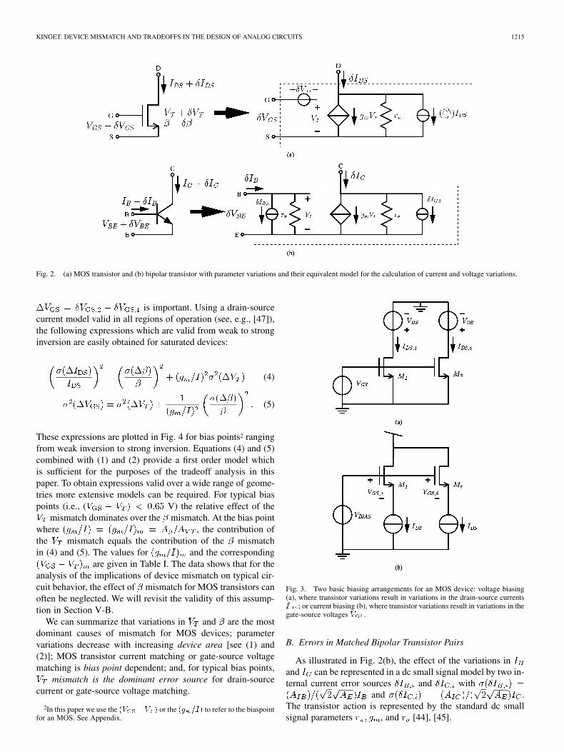
These expressions are plotted in Fig. 4 for bias points2 rangingfrom weak inversion to strong inversion. Equations (4) and (5)combined with (1) and (2) provide a first order model whichis sufficient for the purposes of the tradeoff analysis in thispaper. To obtain expressions valid over a wide range of geome-tries more extensive models can be required. For typical biaspoints (i.e., ( V) the relative effect of the
mismatch dominates over the mismatch. At the bias pointwhere , the contribution ofthe mismatch equals the contribution of the mismatchin (4) and (5). The values for and the corresponding
are given in Table I. The data shows that for theanalysis of the implications of device mismatch on typical cir-cuit behavior, the effect of mismatch for MOS transistors canoften be neglected. We will revisit the validity of this assump-tion in Section V-B.
We can summarize that variations in and are the mostdominant causes of mismatch for MOS devices; parametervariations decrease with increasing device area [see (1) and(2)]; MOS transistor current matching or gate-source voltagematching is bias point dependent; and, for typical bias points,
mismatch is the dominant error source for drain-sourcecurrent or gate-source voltage matching.
2In this paper we use the (V �V ) or the (g =I) to refer to the biaspointfor an MOS. See Appendix.
Fig. 3. Two basic biasing arrangements for an MOS device: voltage biasing(a), where transistor variations result in variations in the drain-source currentsI ; or current biasing (b), where transistor variations result in variations in thegate-source voltages V .
B. Errors in Matched Bipolar Transistor Pairs
As illustrated in Fig. 2(b), the effect of the variations inand can be represented in a dc small signal model by two in-ternal current error sources and with
and .The transistor action is represented by the standard dc smallsignal parameters , and [44], [45].
1216 IEEE JOURNAL OF SOLID-STATE CIRCUITS, VOL. 40, NO. 6, JUNE 2005
Fig. 4. Drain-source current (�) (a) and gate-source voltage (�) (b) mis-match for a 0.25 �m/0.25 �m nMOS transistor in a 0.25 �m CMOS technologywith A = 6 mV�m and A = 1:85% �m [12]; the contributions from Vmismatch ( ) and � mismatch (�) are also shown separately.
The two basic biasing configurations of Fig. 3 can now berevisited for bipolar devices using the equivalent model fromFig. 2(b) and the following expressions are obtained:
(6)
(7)
where is the thermal voltage ( mV at room tempera-ture); the approximation for assumes a large currentgain and a large output resistance
for the transistor.We can summarize that variations in the base current and
collector current are the most important causes of mismatch inbipolar circuits; transistor variations reduce with increasing de-vice area [see (3)]; the errors are bias point independent; the
collector current mismatch3 is the dominant error source for col-lector current and base-emitter voltage matching.
C. DC Offset Calculation for a Fully Differential OTA
By representing device mismatch as error sources in the dcsmall signal equivalent model as in Fig. 2, the calculation ofthe sensitivity of a circuit to device mismatches and param-eter variations can be reduced to a small signal analysis [42],[43]. As an example we now calculate the input offset voltagefor the fully differential operational transconductance amplifier(OTA) in Fig. 5. First we short the differential outputs and cal-culate the output error current due to the error sources.4
Table II lists the respective multiplication factors5 for the contri-bution of each error source to . We then null the internalerror sources and apply an equivalent input differential offsetvoltage source and again compute the output error current
.The multiplication factors for matched pairs ,
, , have opposite signsso that this fully differential topology cancels any systematicshifts6 in or (i.e., all or are identical). However,random variations result in a random equivalent input offsetvoltage that can be computed by equating and .Now the and are independent stochastic variablesand the variance of depends the sum of the variances in(1) and (2). For most practical bias points the contribution ofthe mismatch can be neglected compared to the mismatchand the following expression is then obtained:
(8)
The equivalent input offset voltage is strongly dependent onthe contribution of the input differential pair. The sensitivity tothe other pairs can be reduced by decreasing and com-pared to . Since in this example all devices are biased withthe same current, this can only be achieved by decreasing the
for and , and thus increasing their ,which comes at the cost of a reduced output swing.
IV. IMPLICATION OF MISMATCH ON THE
PERFORMANCE TRADEOFFS AND DESIGN
OPTIMIZATION OF ANALOG CIRCUITS
In the upcoming paragraphs, the derivations and examplesare for MOS analog circuits. For bipolar circuits very similarderivations can be performed. In the interest of clarity, the dis-cussion of the tradeoffs in bipolar circuits is postponed to a sep-arate paragraph.
3In the examples studied here the base is voltage biased and the contributionof the base current mismatches to the errors is small. However, in bipolar circuitswith very high impedances at the base, the base current mismatch contributioncan be significant.
4By calculating the output current we do not have to include the outputimpedance in the expressions. This calculation technique is similar to tech-niques used in circuit noise analysis (see, e.g., [45]).
5The second-order errors in the current mirrors due to the finite transconduc-tance and output conductance have been neglected.
6With the exception of process gradients which can be addressed by commoncentroid layout techniques.

KINGET: DEVICE MISMATCH AND TRADEOFFS IN THE DESIGN OF ANALOG CIRCUITS 1217
Fig. 5. (a) Schematic of a fully differential operational transconductance amplifier where (M ;M ); (M ;M ); (M ;M ); (M ;M ) are matchedpairs; the common-mode feedback circuit is omitted for clarity. (b) Equivalent circuit for the calculation of the effect of transistor mismatches; the transistor outputresistances r have been omitted for clarity.
TABLE IIMULTIPLICATION FACTORS FOR THE CONTRIBUTIONS
OF THE DIFFERENT MISMATCH SOURCES IN �I
During the design of a MOS circuit the designer has tochoose the current, width and length of the devices. For agiven current and bias point , only the aspect ratio
of the device is fixed, but the width or the length canstill be chosen freely. The use of shorter channel devices helpsto reduce the capacitive load in the circuit. This results in alower power consumption for a given bandwidth or operation
frequency (“speed”) and a reduction in the power-bandwidthratio. However, due to device mismatch there is a minimalrequired device area to achieve a given dc accuracy.This introduces an additional constraint that fixes the minimalarea and thus circuit capacitance. We will show that, as aconsequence, the power-bandwidth ratio cannot be optimizedindependently of the dc accuracy requirements.
In the subsequent paragraphs we derive the connectionbetween dc accuracy, bandwidth and power consumption forseveral basic analog circuit blocks. We only consider mis-matches and collector current mismatches as the dominantsources of error and neglect the effect of and base currentmismatches. This assumption was substantiated in Section IIand will be re-examined in Section V-B. We demonstrate thatthe power-bandwidth-accuracy tradeoff is only weakly depen-dent on the device sizing and mainly depends on technologicaland physical constants. We also investigate the optimal designof these blocks in view of these constraints.

1218 IEEE JOURNAL OF SOLID-STATE CIRCUITS, VOL. 40, NO. 6, JUNE 2005
A. Current Signal Processing Blocks
A current mirror is an important building block for signal pro-cessing and for biasing in many analog circuits. Fig. 6 shows theschematic for a 1-1 current mirror. This is considered a currentprocessing block since the signals of interest are the input cur-rent and the output current; the gate-source voltage that developsis crucial in the operation of the circuit but its value or accuracyis not of direct interest.
Under nominal operation, the output current of the mirroris equal to the input current . Systematic errors can occur,e.g., due to the limited output resistance of the devices. Thesesystematic errors can be corrected during the design stage bytopology improvements (e.g., by using cascode devices) and assuch do not fundamentally limit the accuracy. The random vari-ations in the device parameters result in device mismatches inevery fabricated circuit; these cause dc offsets in the output cur-rent which cannot be corrected during the design phase. To ob-tain a zero output, an input offset current has to be applied whosestandard deviation can be calculated as follows:
(9)
where is the bias current, the transconductance, andand are the width and length of the devices.
In a typical application the relative accuracy of the currentsignal processing depends on the ratio of the maximal inputcurrent signal, , and the value7 of the input referredoffset current . The distortion and linearity requirements8
determine the maximal . We assume a typical bias mod-ulation index of and is then . The dcaccuracy is now
(10)
which illustrates the direct connection between accuracy and thedevice area.
Typically, the bandwidth, which determines the maximalinput signal frequency or speed, and the power consumptionare the other two most significant specifications besides accu-racy. A mirror operating in strong inversion9 has a bandwidth
7By using the 3� value of the offset current, the current mirror meets theaccuracy specification with a probability of about 99.7%. This probability has adirect impact on the yield of the total chip and in complex systems with manystages, a higher probability can be required for the individual stages to obtain ahigh yield [5]–[7]; more than a 3� variation has then to be accounted for in (10).Note however that an increased dc accuracy increases the power consumptionor reduces the bandwidth of the circuit substantially [see (12)].
8Typically, the distortion and linearity specifications determine the magnitudeof the largest signals that can be processed correctly by the circuit. For the sakeof clarity, we assume that the distortion specifications are met under the givenassumptions. If very high linearity is required, only smaller signals comparedto the bias can be used and this will result a lower accuracy or a higher powerconsumption [7].
9This derivation can easily be repeated for devices operating in moderate orweak inversion by using the appropriate value of the gate-source and gate-bulkcapacitances for the bandwidth calculation. Since the optimal performance ofthe current mirror is in strong inversion, we present that case here.
Fig. 6. Current mirror as a basic current signal processing block; M andM are matched devices.
[44]–[46], a power con-sumption and thus a power-bandwidth ratioof
(11)
For a given bias point , using a smaller device area yieldsa lower power consumption and higher bandwidth at the ex-pense of a reduced accuracy. Substituting the minimal devicearea required by the accuracy specifications from (10) into (11)results in the following performance tradeoff relationship:
(12)
The dc accuracy requirement fixes the power-speed ratio of thecircuit and the tradeoff between the bandwidth, the accuracyand the power consumption is set by technology constants
. Operating the mirror toward strong inver-sion by choosing a bias point with a large anda small , is the only design parameter a designer canmodify to improve this tradeoff. Power supply and voltageswing limitations typically do not allow for an improvement farbeyond a factor.
Table III shows the simulation results for the performance offour 1-1 current mirrors in a 0.18 m CMOS technology. A 1-1mirror with m/ m transistors is used as the referencepoint (Ref). The performance of three modified mirrors (LP, HS,HA) all operating at about the of the Ref mirror aresimulated as well. The LP mirror is sized toward lower powerconsumption, the HS mirror is sized for high speed and the HAmirror transistor sizes are chosen to improve the accuracy. Thesimulations confirm that LP, HS and HA mirrors have indeedthe same ratio since they operate at the same
. The ratio for the Ref mirror is abouttwice the other mirrors’ ratio which is consistent with (12) andits being twice as large.
B. Voltage Signal Processing Blocks
To study the implications of device mismatches for circuitsthat process voltage signals we consider two different circuit ar-chitectures: open loop and feedback (or closed loop) topologies.
1) Open Loop Topologies: Many important voltage signalprocessing circuits rely on an open loop circuit topology. Forinstance, in high-speed flash analog-to-digital converters [5] the

KINGET: DEVICE MISMATCH AND TRADEOFFS IN THE DESIGN OF ANALOG CIRCUITS 1219
TABLE IIICOMPARISON OF THE SIMULATED PERFORMANCE FOR DIFFERENT 1-1
CURRENT MIRRORS IN A 0.18-�m CMOS TECHNOLOGY
input signal is compared with different reference voltages in par-allel. A simplified block diagram is illustrated in Fig. 7; the inputsignal is buffered by the input block which often consists ofa “Sample-and-Hold” followed by a buffer; this buffer drivesthe input of blocks which can be pre-amplifiers orcomparators.
The accuracy of the signal processing depends on the offsetvoltages of whose input stages invariably consistof differential pairs. A typical measure for the accuracy is then
(13)
where is the signal level at the buffer output, andand are the width and length of the input devices. Again, toimprove the accuracy, the area of the input device has to beincreased which results in a larger capacitive load at the bufferoutput. For an input pair operating in strong inversion the inputcapacitance for stage is[22] and the dc accuracy and input capacitance are related by
(14)
Interestingly, the numerator in (14) is proportional to the energystored and removed from the input capacitors [5].
The power-bandwidth tradeoff in the circuit of Fig. 7 is setby the total load at the buffer output and the efficiency of thebuffer. For a buffer operating in class A mode, the dc bias currentmust be larger than the signal current amplitude and the supplyvoltage must be larger than twice the signal voltage ampli-tude; a lower bound on the power consumption for a signal withfrequency is then: . Forpractical buffer circuits the power consumption will be largerdue to voltage headroom and distortion requirements. After re-casting this power bound into
(15)
we conclude there is again a bandwidth-accuracy-powertradeoff for this type of circuit.
2) Feedback Topologies: Active electronic devices havestrongly nonlinear characteristics and linear voltage signal
Fig. 7. Open loop voltage signal processing circuit including a buffer B andN identical parallel voltage processing circuits C . . .C .
Fig. 8. Linear voltage amplifier using an opamp in a feedback topology.
processing circuits most often use feedback topologies.The feedback amplifier in Fig. 8 is a representative ex-ample of a feedback voltage amplifier and has a voltage gain
. For the typical case of a large gainamplifier and an input pair operating in stronginversion, the dc accuracy is given by (13) and is proportionalto the input capacitance as in (14). More stringent dcaccuracy requirements lead to larger input devices and a larger
which with the feedback network introduces aparasitic pole in the loop gain transfer function. To maintainstability, this pole needs to be moved to frequencies beyond
times the unity gain bandwidth of the loop where is2 or larger for typical designs [44]–[46]. This requires reducingthe impedances and and results in a larger loading of theamplifier’s output buffer and increases its power consumption.It can be shown that closed loop bandwidth , accuracyand power consumption are again closely tied
(16)
Remarkably, both in (15) and (16) the tradeoff between thedifferent specifications is only determined by technology con-stants and the circuit designer has little influence on this overall

1220 IEEE JOURNAL OF SOLID-STATE CIRCUITS, VOL. 40, NO. 6, JUNE 2005
Fig. 9. Linear voltage amplifier with feedback topology implemented with adifferential pair as a simple operational amplifier.
tradeoff. We now study two circuit level realizations for Fig. 8to find circuit design guidelines that improve the tradeoff.
a) Two Transistor Differential Amplifier: Fig. 9 shows acircuit implementation of Fig. 8 using a differential pair as asimple operational amplifier. For very high-precision designslarge input devices are required and the gate capacitance is thedominant capacitance in this circuit; we neglect the effects ofthe other capacitors in this first order analysis. The bandwidthof the circuit is then set by . The powerconsumption is given by and the maximumoutput signal is a fraction of the available supply voltage or
where is the closedloop gain and is a parameter smaller than one that de-creases with more stringent linearity requirements for the de-sign. Combining these relationships with the expression for thedc accuracy and input capacitance (14) the following tradeoffrelationship is obtained:
(17)
Interestingly, the best combined performance for this voltagemode circuit when gain, speed, accuracy and power consump-tion are considered, is obtained if the stage is designed with alarge or small .
b) Load Compensated Operational TransconductanceAmplifier: Operational transconductance amplifiers are widelyused in closed loop voltage circuits and Fig. 5 shows a rep-resentative schematic. A load-compensated OTA typicallyconsists of a differential voltage to current input stage (and ) and a current-in current-out output stage (and ) [44], [46], [48]. For this derivation we assumethe effect of the internal poles of the OTA on the stabilitydominate over the effect of the pole created by the feedbacknetwork and the input capacitance; the influence of the inputpole was investigated earlier. In differential mode, this OTAhas a nondominant pole at the gates of (and ),
, which together with therequired stability limits the maximum Gain-Bandwidth productthat can be used, and , whereis the closed loop gain and is typically 2 or larger toguarantee a sufficient phase margin. The offset voltage of thisamplifier is given by (8) and assuming that all transistors have
the same length ,10 that and thus , andthat the current source devices and are made suffi-ciently large so that their contribution to the offset is negliblewe can rewrite (8) as follows:
(18)
Combining these relationships and the earlier expressions for dcaccuracy and maximum input signal with the expression for thepower consumption, , we find the followingtradeoff:
(19)
Once more the bandwidth, accuracy, and power consump-tion of this circuit are closely linked and set by the technologymatching quality. The only step the designer can take to improvethe overall performance is to maximize and minimize
, which implies maximizing the internal small signalgain from the inputs to the gates of and . This is fullyin line with previous circuit sizing optimizations which steeredtoward a high for voltage signal processing transistorsand a low for current processing transistors.
C. MOS Analog Circuit Performance Limitations and BiasPoint Optimization
The presented analysis of the tradeoffs in the design of analogcurrent and voltage signal processing circuits [see (12), (15),(17), and (19)] leads to the following conclusions:
• The bandwidth-accuracy-power tradeoff is almost inde-pendent of design parameters and is bound by the tech-nology parameter .
• Optimizing the MOS bias point allows simultaneous im-provement off both the accuracy and the bandwidth-accu-racy-power tradeoff:
— in current signal processing by using a small andlarge (see (12), and (19));
— in voltage signal processing by using a large andsmall (see (17), and (19)).
D. Matching Tradeoffs in Bipolar Circuits
The results obtained for the MOS circuits can easily beadapted for the case of bipolar devices. The tradeoffs in a bipolarcurrent mirror using a similar topology as in Fig. 6 are derivedhere. For devices with an emitter area and with a largecurrent gain , the offset current is
. In a typical high accuracy, analog application thebipolar devices are biased in their ideal operation region and
10The length of the current mirror transistors is typically kept as small as pos-sible to maintain a high bandwidth and second pole; also for the input devicessmall lengths are desirable to obtain a large (g =I). A possible reason to in-crease the device length is to reduce mismatch degradation due to short channeleffects, but this will lead to a larger length for both the input and current mirrordevices since both contribute considerably. So, the assumption of similar lengthsis typically valid.

KINGET: DEVICE MISMATCH AND TRADEOFFS IN THE DESIGN OF ANALOG CIRCUITS 1221
operate below their peak transit frequency so that theinput capacitance is dominated by the junction capacitancebetween base and emitter. The bandwidth of the mirror isthen [44], [45] withthe base-emitter junction capacitance per unit emitter area.Combining the expressions for offset current, accuracy (10),power consumption, and bandwidth, the following relationshipis obtained:
(20)
which is very similar to the case of an MOS current mirror.The voltage signal processing examples can be repeated in
a similar manner for bipolar devices. E.g., for a bipolar inputpair operating below peak- the input capacitance is
and the relationship between input capacitance anddc accuracy similar to (14) now becomes
(21)
The tradeoffs for the different circuits are very similar exceptthat for the bipolar devices the ratio is bias independent,so that no bias point optimization is possible in contrast to theMOS case.
V. IMPLICATIONS FOR ANALOG SYSTEM PERFORMANCE
AND TECHNOLOGY SCALING
A. Power Limitations for Analog Signal Processing: NoiseVersus Offset
In an analog circuit, the smallest signal that is correctly pro-cessed can be limited by device mismatches and offset or bynoise. We now compare these limitations.
First, the contribution of the input stages to the overall systemoffset dominates over the contribution of later stages providedsufficient gain exists in the stages11 [7]. At the input stage, thesignals are small and the effects of offset on accuracy are morepronounced. Low offset design thus leads to similar design con-siderations as low noise design (see, e.g., [44], [45]).
As demonstrated in Section IV-B there is a strong couplingbetween the required dc accuracy and the input capacitance; (14)shows that the required signal energy to drive the capacitor isproportional to the dc accuracy requirements. The associatedpower drain sets the theoretical minimal power drain for thegiven accuracy and speed. For a 100% efficient class B system,the power required to drive a signal with a frequency
across a capacitor is [49]:which after insertion of (14) and (21) results in the followingexpressions for the power consumption:
(22)
(23)
The matching quality of the technology puts a lower boundaryon the minimal power drain of analog systems and thebandwidth-accuracy-power tradeoff depends on technologicalconstants.
11The analysis of the OTA in Section IV-B.2b has similar conclusions.
Thermal noise also sets a lower limit on the smallest signalthat can be processed by the circuit and in [49] it is demonstratedthat this results in a boundary on the minimal power drain foran analog system for a given signal frequency and a givensignal-to-noise ratio
(24)
where is the Boltzmann constant and the absolutetemperature.
The limits on the minimal energy per cycle P/f imposedby noise (24), and by mismatch (22) and (23) are plotted inFig. 10(a). The limits imposed by mismatch are technology de-pendent. For MOS circuits the limit is more than two orders ofmagnitude higher than the limit imposed by thermal noise [4].The limit for bipolar circuits12 is about two orders of magnitudesmaller than for MOS circuits and is very close to the noiseimposed limit. The ratio of the “matching energy” [8], [11],
, to the thermal noise energy, , is plotted for severalMOS technology nodes in Fig. 10(b). Down to submicron MOStechnologies, is more than 10 to 100 times . Weconclude that in MOS integrated circuits that are sensitive todc accuracy, offsets due to device mismatches and not thermalnoise set the limit for the smallest signal that can be processed.On the other hand, bipolar circuits have a much higher intrinsicaccuracy than MOS circuits and the limits imposed by noiseand offsets are very close.
B. MOS Technology Scaling
A downwards evolution of with shrinking MOS devicesize can be observed in Fig. 1. The fluctuation of the dopantatoms under the gate has been demonstrated to be an impor-tant source of mismatch for MOS devices; a smaller gateoxide thickness results in a smaller but a higher sub-strate doping level leads to a larger [18], [50]. Technologyscaling indeed reduces the which leads to a reduction inbut this reduction is somewhat decreased by the increase in thesubstrate doping level needed in deep-submicron devices. Noclear trend in the evolution of can be identified in Fig. 1.The current factor mismatch has been linked to mobilityfluctuations [18] but a good physical understanding and a linkto technology parameters is still missing.
In the analysis for MOS circuits presented in this papermismatch has been used as the dominant cause of errors. Thisassumption is correct as long as the of the deviceis smaller than (see Section III-A). In Table I thevalues of are presented for different technolo-gies and a downward trend for can be observed.Due to signal swing requirements and biasing limitations, the
used in practical circuits will indeed be (substan-tially) smaller than for the presented technologies.Taking into account the significant reduction of supply voltageswith MOS technology scaling [51], this will most probably re-main so for several technology nodes to come. Additionally wenote that the basic assumption for the derivations in this paper isthe area dependence of the device matching. Independently of
12A typical value of 3 fF/�m was assumed for C (see, e.g., [45,Fig. 1.25])

1222 IEEE JOURNAL OF SOLID-STATE CIRCUITS, VOL. 40, NO. 6, JUNE 2005
Fig. 10. (a) Comparison of the minimal power limit imposed by mismatch (22)for a 1.2 �m (}), 0.7 �m ( ), 0.18 �m ( ), and bipolar (�) technology andthe limit imposed by thermal noise (x) versus Acc and SNR . (b) Ratioof the “matching energy” to the “noise energy” over several MOS technologynodes.
or mismatch being dominant, or both being significant, thearea dependence of the mismatch leads to a fixed bandwidth-ac-curacy-power constraint [7].
The bias point optimization of voltage processing circuitspromotes using a low or high so thatmismatch errors are indeed more dominant. Thereduction is typically limited by the bandwidth requirements ofthe application due to a decrease of the transistor transit fre-quency for smaller and larger [22], [44],[52]. For high-speed circuits the minimum is set bythe bandwidth (and device ) requirements which results in aquadratic dependence of the power consumption on the band-width rather than the linear dependence as in (17) [7].
Current processing circuits perform better when biased witha large (or low ) and this can lead in somecases to a significant contribution from the mismatch errors.An optimization of the current mirror performance using the fullexpression for the drain-source current error from (4) concludesthat (or ) is the optimal bias point [7].Using a bias point with a large leads to an increase in
Fig. 11. �(�V )( ) and �(��=�)(}) for a minimal nMOS device indifferent technology nodes.
the errors and reduces the performance. However, due to supplyvoltage constraints and output swing requirements, current mir-rors can typically not be biased at the high levels.
The reduction of with smaller results in a reductionof the matching energy with the technology featuresize as shown in Fig. 10(b). This apparent advantage of tech-nology scaling for analog circuits is strongly offset however bythe reduction of the power supply voltages. Reducing the powersupply voltage leads to a linear reduction in the power consump-tion, but also entails a reduction in the signal swing. This resultsin a quadratic reduction of the dc Accuracy. The Bandwidth-Ac-curacy-Power tradeoff degrades for lower supply voltages as canbe seen, e.g., in (17) and (19).
The reduction of with feature size implies that thematching for devices occupying a constant area improves indeeper sub-micron technologies so that, for the same accuracyrequirements, some area scaling of transistors is possible. But,this scaling advantage typically vanishes due to the aggressivepower supply voltage scaling as discussed above. Moreover,the area of the minimal size device reduces quadraticallywith the feature size whereas the reduction in is onlylinear. Consequently the matching of the minimal size device
degrades with scalingas can be seen from Fig. 11 for nMOS transistors. This isan important concern for the design of digital circuits sincethe device mismatch starts affecting the noise margin [8] andmismatch mitigation techniques (discussed next) cannot bewidely applied due to their large area overhead.
C. Mitigation of the Effect of Device Mismatch
The strong power consumption constraints imposed bymatching demonstrated in this paper provide a quantitativejustification for the use of offset correction techniques in MOScircuits. It is highly desirable to mitigate the effect of devicemismatch on the accuracy performance of the analog signalprocessing. Since device mismatch is caused by randomnessin fabrication processes, the device mismatches can only becorrected after device fabrication. Post fabrication trimming ofthe individual devices requires special IC technology options
KINGET: DEVICE MISMATCH AND TRADEOFFS IN THE DESIGN OF ANALOG CIRCUITS 1223
as well as expensive test equipment and test time and is onlyeconomical in some high-end applications.
Auto-zero calibration or chopping techniques [53] can berealized without special technology modifications but do requirethat the signal processing is interrupted and the circuit is takenoff-line on a regularbasis. The ultimate limitation of these correc-tion techniques again becomes the matching accuracy betweencomponents such as, e.g., switches [53] but the system accuracycan be improved significantly. Another possibility is to decouplethe interdependence of bandwidth, accuracy and power con-sumption with circuit architecture modifications. For example,in current-steering digital-to-analog converters [6], the accuracyrequirements and speed performance are less strongly coupledsince they are set by different devices.This helps in alleviating thedevice mismatch imposed performance boundaries. Averaging[54] in analog-to-digital converters reduces the effects of noiseand mismatch without significant operation speed penalties.Other approaches suggest to fabricate a large set of redundantdevices and select the optimal devices post fabrication [55].
VI. CONCLUSIONS
The matching of devices is proportional to their area anthus their capacitance and, consequently, the accuracy require-ments for analog circuits impose a minimal circuit area andcapacitance; the power required to achieve a given bandwidthincreases with the circuit capacitance. This paper shows that,as a result, the bandwidth-accuracy-power tradeoff is fixed bytechnology constants, related to the device matching quality.This constraint was derived for general MOS and bipolar analogcircuits including current processing and voltage processingcircuits.
The bandwidth-accuracy-power tradeoff can be improved inMOS current processing circuits by choosing a bias point witha high and low ; MOS voltage processingcircuits should be designed as low a (or as high a
) as possible. In bipolar circuits the performance tradeoffis largely independent of the bias point.
For a given bandwidth and accuracy the limit on the minimumpower consumption imposed by device matching is about twoorders of magnitude larger than the limit imposed by noise formodern MOS processes. For bipolar technologies the noise andmismatch limits are similar.
APPENDIX
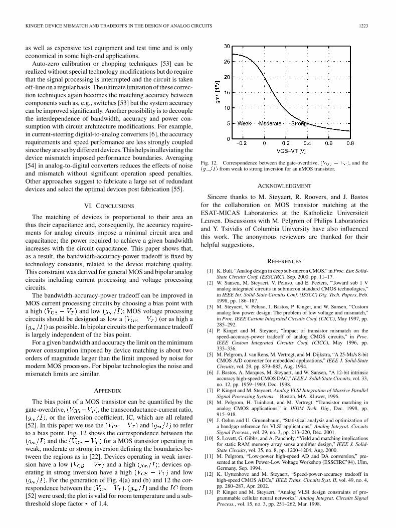
The bias point of a MOS transistor can be quantified by thegate-overdrive, , the transconductance-current ratio,
, or the inversion coefficient, IC, which are all related[52]. In this paper we use the and to referto a bias point. Fig. 12 shows the correspondence between the
and the for a MOS transistor operating inweak, moderate or strong inversion defining the boundaries be-tween the regions as in [22]. Devices operating in weak inver-sion have a low and a high ; devices op-erating in strong inversion have a high and low
. For the generation of Fig. 4(a) and (b) and 12 the cor-respondence between the and the from[52] were used; the plot is valid for room temperature and a sub-threshold slope factor of 1.4.
Fig. 12. Correspondence between the gate-overdrive, (V � V ), and the(g =I) from weak to strong inversion for an nMOS transistor.
ACKNOWLEDGMENT
Sincere thanks to M. Steyaert, R. Roovers, and J. Bastosfor the collaboration on MOS transistor matching at theESAT-MICAS Laboratories at the Katholieke UniversiteitLeuven. Discussions with M. Pelgrom of Philips Laboratoriesand Y. Tsividis of Columbia University have also influencedthis work. The anonymous reviewers are thanked for theirhelpful suggestions.
REFERENCES
[1] K. Bult, “Analog design in deep sub-micron CMOS,” in Proc. Eur. Solid-State Circuits Conf. (ESSCIRC), Sep. 2000, pp. 11–17.
[2] W. Sansen, M. Steyaert, V. Peluso, and E. Peeters, “Toward sub 1 Vanalog integrated circuits in submicron standard CMOS technologies,”in IEEE Int. Solid-State Circuits Conf. (ISSCC) Dig. Tech. Papers, Feb.1998, pp. 186–187.
[3] M. Steyaert, V. Peluso, J. Bastos, P. Kinget, and W. Sansen, “Customanalog low power design: The problem of low voltage and mismatch,”in Proc. IEEE Custom Integrated Circuits Conf. (CICC), May 1997, pp.285–292.
[4] P. Kinget and M. Steyaert, “Impact of transistor mismatch on thespeed-accuracy-power tradeoff of analog CMOS circuits,” in Proc.IEEE Custom Integrated Circuits Conf. (CICC), May 1996, pp.333–336.
[5] M. Pelgrom, J. van Rens, M. Vertregt, and M. Dijkstra, “A 25-Ms/s 8-bitCMOS A/D converter for embedded applications,” IEEE J. Solid-StateCircuits, vol. 29, pp. 879–885, Aug. 1994.
[6] J. Bastos, A. Marques, M. Steyaert, and W. Sansen, “A 12-bit intrinsicaccuracy high-speed CMOS DAC,” IEEE J. Solid-State Circuits, vol. 33,no. 12, pp. 1959–1969, Dec. 1998.
[7] P. Kinget and M. Steyaert, Analog VLSI Integration of Massive ParallelSignal Processing Systems. Boston, MA: Kluwer, 1996.
[8] M. Pelgrom, H. Tuinhout, and M. Vertregt, “Transistor matching inanalog CMOS applications,” in IEDM Tech. Dig., Dec. 1998, pp.915–918.
[9] J. Oehm and U. Gruenebaum, “Statistical analysis and optimization ofa bandgap reference for VLSI applications,” Analog Integrat. CircuitsSignal Process., vol. 29, no. 3, pp. 213–220, Dec. 2001.
[10] S. Lovett, G. Gibbs, and A. Pancholy, “Yield and matching implicationsfor static RAM memory array sense amplifier design,” IEEE J. Solid-State Circuits, vol. 35, no. 8, pp. 1200–1204, Aug. 2000.
[11] M. Pelgrom, “Low-power high-speed AD and DA conversion,” pre-sented at the Low Power-Low Voltage Workshop (ESSCIRC’94), Ulm,Germany, Sep. 1994.
[12] K. Uyttenhove and M. Steyaert, “Speed-power-accuracy tradeoff inhigh-speed CMOS ADCs,” IEEE Trans. Circuits Syst. II, vol. 49, no. 4,pp. 280–287, Apr. 2002.
[13] P. Kinget and M. Steyaert, “Analog VLSI design constraints of pro-grammable cellular neural networks,” Analog Integrat. Circuits SignalProcess., vol. 15, no. 3, pp. 251–262, Mar. 1998.

1224 IEEE JOURNAL OF SOLID-STATE CIRCUITS, VOL. 40, NO. 6, JUNE 2005
[14] A. Rodriguez-Vazquez, G. Linan, S. Espejo, and R. Dominguez-Castro,“Mismatch-induced tradeoffs and scalability of mixed-signal visionchips,” in Proc. IEEE Int. Symp. Circuits and Systems (ISCAS), 2002,pp. V-93–V-96.
[15] M. Bolt, E. Cantatore, M. Socha, C. Aussems, and J. Solo, “Matchingproperties of MOS transistors and delay line chains with self-alignedsource/drain contacts,” in Proc. IEEE Int. Conf. Microelectronic TestStructures, Mar. 1996, pp. 21–25.
[16] J. Shyu, G. C. Temes, and F. Krummenacher, “Random error effectsin matched MOS capacitors and current sources,” IEEE J. Solid-StateCircuits, vol. SC-19, no. 6, pp. 948–955, Dec. 1984.
[17] K. R. Lakshmikumar, R. A. Hadaway, and M. A. Copeland, “Char-acterization and modeling of mismatch in MOS transistors for preci-sion analog design,” IEEE J. Solid-State Circuits, vol. 21, no. 6, pp.1057–1066, Dec. 1986.
[18] M. Pelgrom, A. Duinmaijer, and A. Welbers, “Matching propertiesof MOS transistors,” IEEE J. Solid-State Circuits, vol. 24, no. 5, pp.1433–1439, May 1989.
[19] J. Bastos, M. Steyaert, R. Roovers, P. Kinget, W. Sansen, B. Grain-dourze, N. Pergoot, and E. Janssens, “Mismatch characterization ofsmall size MOS transistors,” in Proc. IEEE Int. Conf. MicroelectronicTest Structures, Mar. 1995, pp. 271–276.
[20] J. Horstmann, U. Hilleringmann, and K. Goser, “Matching analysis ofdeposition defined 50-nm MOSFET’s,” IEEE Trans. Electron Devices,vol. 45, no. 1, pp. 299–306, Jan. 1998.
[21] T.-H. Yeh, J. Lin, S.-C. Wong, H. Huang, and J. Sun, “Mis-match char-acterization of 1.8 V and 3.3 V devices in 0.18 �m mixed signal CMOStechnology,” in Proc. IEEE Int. Conf. Microelectronic Test Structures,Mar. 2001, pp. 77–82.
[22] Y. Tsividis, Operation and Modeling of the MOS Transistor, 2nded. Oxford, U.K.: Oxford Univ. Press, 2003.
[23] L. Portmann, C. Lallement, and F. Krummenacher, “A high density inte-grated test matrix of MOS transistors for matching study,” in Proc. IEEEInt. Conf. Microelectronic Test Structures, Mar. 1998, pp. 19–24.
[24] U. Gruenebaum, J. Oehm, and K. Schumacher, “Mismatch modelingand simulation—A comprehensive approach,” Analog Integrat. CircuitsSignal Process., vol. 29, no. 3, pp. 165–171, Dec. 2001.
[25] M. Steyaert, J. Bastos, R. Roovers, P. Kinget, W. Sansen, B. Grain-dourze, N. Pergoot, and E. Janssens, “Threshold voltage mismatch inshort-channel MOS transistors,” Electron. Lett., vol. 30, pp. 1546–1548,Sep. 1994.
[26] J. Bastos, M. Steyaert, A. Pergoot, and W. Sansen, “Mismatch character-ization of submicron MOS transistors,” Analog Integrat. Circuits SignalProcess., vol. 12, no. 2, pp. 95–106, Feb. 1997.
[27] S. Lovett, M. Welten, A. Mathewson, and B. Mason, “Optimizing MOStransistor mismatch,” IEEE J. Solid-State Circuits, vol. 33, no. 1, pp.147–150, Jan. 1998.
[28] P. Drennan and C. McAndrew, “Understanding MOSFET mismatch foranalog design,” IEEE J. Solid-State Circuits, vol. 38, no. 3, pp. 450–456,Mar. 2003.
[29] J. Croon, M. Rosmeulen, S. Decoutere, W. Sansen, and H. Maes, “Aneasy-to-use mismatch model for the MOS transistor,” IEEE J. Solid-State Circuits, vol. 37, no. 8, pp. 1056–1064, Aug. 2002.
[30] F. Forti and M. Wright, “Measurement of MOS current mismatch in theweak inversion region,” IEEE J. Solid-State Circuits, vol. 29, no. 2, pp.138–142, Feb. 1994.
[31] A. Pavasovic, A. G. Andreou, and C. R. Westgate, “Characterization ofsubthreshold MOS mismatch in transistors for VLSI systems,” AnalogIntegrat. Circuits Signal Process., no. 6, pp. 75–85, 1994.
[32] J. Bastos, “Matching characterization of MOS transistors for analog de-sign,” Ph.D. dissertation, Katholieke Univ., Leuven, Belgium, 1998.
[33] J. P. de Gyvez and H. Tuinhout, “Threshold voltage mismatch andintra-die leakage current in digital CMOS circuits,” IEEE J. Solid-StateCircuits, vol. 39, no. 1, pp. 157–168, Jan. 2004.
[34] J. Bastos, M. Steyaert, B. Graindourze, and W. Sansen, “Matching ofMOS transistors with different layout styles,” in Proc. IEEE Int. Conf.Microelectronic Test Structures, Mar. 1996, pp. 17–18.
[35] H. Tuinhout, M. Pelgrom, R. P. de Vries, and M. Vertregt, “Effects ofmetal coverage on MOSFET matching,” in IEDM Tech. Dig., Dec. 1996,pp. 735–738.
[36] H. Tuinhout and M. Vertregt, “Characterization of systematicMOSFET current factor mismatch caused by metal CMP dummystructures,” IEEE Trans. Semiconduct. Manufact., vol. 14, no. 4, pp.302–310, Nov. 2001.
[37] J. Bastos, M. Steyaert, A. Pergoot, and W. Sansen, “Influence of die at-tachment on MOS transistor matching,” IEEE Trans. Semiconduct. Man-ufact., vol. 10, no. 2, pp. 209–218, May 1997.
[38] H. Tuinhout, “Improving BiCMOS technologies using BJT parametricmismatch characterization,” in Proc. Bipolar/BiCMOS Circuits andTechnology Meeting, Sep. 2003, pp. 163–170.
[39] G. Lau, W. Einbrodt, and W. Sieber, “Improvement of poly emittern-p-n transistor matching in a 0.6 micron mixed signal technology,” inProc. IEEE Int. Conf. Microelectronic Test Structures, Mar. 2003, pp.232–237.
[40] P. Drennan, C. McAndrew, J. Bates, and D. Schroder, “Rapid evaluationof the root causes of BJT mismatch,” in Proc. IEEE Int. Conf. Micro-electronic Test Structures, Mar. 2000, pp. 122–127.
[41] H. Tuinhout, A. Bretveld, and W. Peters, “Current mirror test structuresfor studying adjacent layout effects on systematic transistor mismatch,”in Proc. IEEE Int. Conf. Microelectronic Test Structures, Mar. 2003, pp.221–226.
[42] J. Oehm and K. Schumacher, “Quality assurance and upgrade of analogcharacteristics by fast mismatch analysis option in network analysis en-vironment,” IEEE J. Solid-State Circuits, vol. 28, no. 7, pp. 865–871,Jul. 1993.
[43] P. Kinget, “Circuit analysis for device parameter variations and mis-match,” , 2005, submitted for publication.
[44] K. Laker and W. Sansen, Design of Analog Integrated Circuits and Sys-tems. New York, NY: McGraw-Hill, 1994.
[45] P. R. Gray, P. J. Hurst, S. H. Lewis, and R. G. Meyer, Analysis and Designof Analog Integrated Circuits. New York, NY: Wiley, 2001.
[46] B. Razavi, Design of Analog CMOS Integrated Circuits. New York,NY: McGraw-Hill, 2001.
[47] Y. Tsividis, K. Suyama, and K. Vavelidis, “Simple ‘reconciliation’MOSFET model valid in all regions,” Electron. Lett., vol. 31, no. 6, pp.506–508, 1995.
[48] P. R. Gray and R. G. Meyer, Analysis and Design of Analog IntegratedCircuits. New York, NY: Wiley, 1984.
[49] E. Vittoz, “Future of analog in the VLSI environment,” in Proc. ISCAS,May 1990, pp. 1372–1375.
[50] T. Mizuno, J. Okamura, and A. Toriumi, “Experimental study ofthreshold voltage fluctuation due to statistical variation of channeldopant number in MOSFET’s,” IEEE Trans. Electron Devices, vol. 41,no. 11, pp. 2216–2221, Nov. 1994.
[51] The International Technology Roadmap for Semiconductors (2001 Edi-tion) [Online]. Available: http://public.itrs.net
[52] D. Binkley, C. Hopper, S. Tucker, B. Moss, J. Rochelle, and D. Foty, “ACAD methodology for optimizing transistor current and sizing in analogCMOS design,” IEEE Trans. Computer-Aided Design, vol. 22, no. 2, pp.225–237, Feb. 2003.
[53] C. Enz, E. Vittoz, and F. Krummenacher, “A CMOS chopper amplifier,”IEEE J. Solid-State Circuits, vol. 22, no. 3, pp. 335–342, Mar. 1987.
[54] K. Kattmann and J. Barrow, “A technique for reducing differential non-linearity errors in flash A/D converters,” in IEEE Int. Solid-State CircuitsConf. Dig. Tech. Papers, Feb. 1991, pp. 170–171.
[55] M. Flynn, C. Donovan, and L. Sattler, “Digital calibration incorporatingredundancy of flash ADCs,” IEEE Trans. Circuits Syst. II, vol. 50, no. 5,pp. 205–213, May 2003.
[56] A. V. den Bosch, M. Steyaert, and W. Sansen, “A high density matchedhexagonal transistor structure in standard CMOS technology for highspeed applications,” in Proc. IEEE Int. Conf. Microelectronic Test Struc-tures, Mar. 1999, pp. 212–215.
Peter R. Kinget (S’88–M’90–SM’02) received theengineering degree in electrical and mechanical engi-neering and the Ph.D. degree in electrical engineeringfrom the Katholieke Universiteit Leuven, Belgium, in1990 and 1996, respectively.
From 1991 to 1995, he held a fellowship fromthe Belgian National Fund for Scientific Research(NFWO) to work as a Research Assistant at theESAT-MICAS Laboratory of the Katholieke Uni-versiteit Leuven. From 1996 to 1999, he was withBell Laboratories, Lucent Technologies, Murray
Hill, NJ, as a Member of Technical Staff in the Design Principles Department.From 1999 to 2002, he held various technical and management positions in ICdesign and development at Broadcom, CeLight, and MultiLink. In the summerof 2002, he joined the faculty of the Department of Electrical Engineering,Columbia University, New York, NY. His research interests are in analog andRF integrated circuits and signal processing.
Dr. Kinget serves on the Technical Program Committees of the IEEE CustomIntegrated Circuits Conference (CICC) and of the Symposium on VLSI Circuits.He has been an Associate Editor for the JOURNAL OF SOLID-STATE CIRCUITS
since 2003.