Embed Size (px)
Citation preview
USOO8440973B1
(12) United States Patent (10) Patent No.: US 8.440,973 B1 Fernandez et al. 45) Date of Patent: MaV 14, 2013 9
(54) BIMORPH CANTILEVER ARRANGEMENT OTHER PUBLICATIONS AND APPLICATIONS THEREOF
F. J. Morin; Oxides which show a metal-to-insulator transition at the (75) Inventors: Felix E Fernandez, Mayaguez, PR (US); neel temperature; Physical Review Letters; Jul. 1, 1959: pp. 34-36;
Nelson Sepulveda-Alancastro, vol. 3, No. 1; U.S. Mayaguez, PR (US); Armando Rua, N. Berglund and H. H. Guggenheim, Electronic Properties of VO Yauco, PR (US); Rafmag Cabrera near the Semiconductor-Metal Transition; Physical Review Sep. 15,
s s s 1969: pp. 1022-1033; vol. 185, No. 5; US. Aguas Buenas, PR (US) D. P. Partlow, S. R. Gurkovich, K. C. Radford, and L. J. Denes;
Switchable fanadium oxide films by a sol-gel process.J. Appl. Phys; (73) Assignee: University of Puerto Rico, San Juan, PR Jul. 1, 1991; pp. 443-452; vol. 70, R. 1.; SP ppi. Iny
(US) J. R. Barnes, R. J. Stephenson, C. N. Woodburn, S.J. O'Shea, M. E. Welland, T. Rayment, J. K. Gimzewski, and CH. Gerber; A
(*) Notice: Subject to any disclaimer, the term of this femtojoule calorimeter using micromechanical sensors; Rev. Sci. patent is extended or adjusted under 35 Instrum.; Dec. 1994; pp. 3793-3798; vol. 65, No. 12; US. U.S.C. 154(b) by 571 days. P. G. Datskos, P.I. Oden, T. Thundat, E. A. Wachter, R. J. Warmack,
and S. R. Hunter; Remote infared radiation detection using (21) Appl. No.: 12/660,933 piezoresistive microcantilevers; Appl Phys. Lett.; Nov. 11, 1996; pp.
2986-2988; vol. 69, No. 20; US. (22) Filed: Mar. 5, 2010 (Continued)
Related U.S. Application Data Primary Examiner — Mark RGaworecki (60) Provisional application No. 61/157,675, filed on Mar. (74) Attorney, Agent, or Firm — Hoglund & Pamias, PSC:
5, 2009. Roberto J. Rios
(51) Int. Cl. (57) ABSTRACT e 1nVent1On ult11ZeS the Changes 1n S1Cal orOpert1eS O GOL 5/20 (2006.01) The i ili he changes in physical properties of
(52) U.S. Cl. materials during a solid-solid phase transition in order to USPC ....................................................... 250/338.4 enhance the sensitivity of cantilever IR detectors. The sub
(58) Field of Classification Search .................. 250/332, stantial changes in properties during insulator-to-metal tran 250/338.1, 338.4, 339.01, 339.02, 339.04 sitions (IMTs) of some materials are useful for controlling
See application file for complete search history. purposes according to the invention. A cantilever arrange (56) Ref Cited ment is provided with a cantilever being coated with an insu
eerees e
U.S. PATENT DOCUMENTS
6,140,646 A 10, 2000 Busta et al. 6,335,478 B1 1/2002 Chou et al. 6,392.233 B1 5, 2002 Channinet al. 6,399,947 B2 6/2002 Yagyu et al. 6,835,932 B2 * 12/2004 Ishizuya et al. ............ 250/338.1 7,184,200 B2 2/2007 Dalakos et al.
lator-to-metal transitions (IMTs) material. Bending of the cantilever is achieved when the temperature of the (IMTs) material is within its phase transition temperature range. A Focal Plane Array (FPA) for detecting Infrared (IR) radiation including the cantilever arrangement of the invention is also proposed.
34 Claims, 6 Drawing Sheets
US 8440,973 B1 Page 2
OTHER PUBLICATIONS
P. I. Oden, P. G. Datskos, T. Thundat and R. J. Warmack; Uncooled thermal imaging using a piezoresistive microcantilever, Appl Phys. Lett.; Nov. 18, 1996; pp. 3277-3279; vol. 69, No. 21; US. S. R. Manalis, S. C. Minne, and C. F. Quate, G. G. Yaralioglu, and A. Atalar; Two-dimensional micromechanical bimorph arrays for detec tion of thermal radiation. Appl Phys. Lett.; Jun. 16, 1997; pp. 3311 3313; vol. 70, No. 24; US. J. Varesi, J. Lai, T. Perazzo, Z. Shi, and A. Majumdar; Photothermal measurements at picowatt resolution using uncooled micro optomechanical sensors; Appl Phys. Lett.; Jul. 21, 1997; pp. 306-308; vol. 71, No. 3; US. Qing-Ming Wang, Xiao-Hong Du, Baomin Xu and Eric Cross; Theo retical analysis of the sensor effect of cantilever piezoelectric bend ers; Journal of Applied Physics; Feb. 1, 1999: pp. 1702-1712; vol. 85, No. 3; US. Perazzo, M. Mao, O. Kwon, A. Majumdar, J. B. Varesi, and P. Norton; Infrared vision using uncooled micro-optomechanical camera; Applied Physics Letters; Jun. 7, 1999: pp.3567-3569; vol. 74, No. 23; US. Nelson Sepulveda, Armando Rua, Rafimag Cabrera, and Felix Fernandez; Young's modulus of VO, thin films as a function of temperature including insulator-to-metal transition regime, Applied Physics Letters; 2008; pp. 191913-1-191913-3; vol.92, No. 19; US. P. G. Datskos, N. V. Lavrik, and S. Rajic; Performance of uncooled microcantilever thermal detectors; Review of Scientific Instruments; Apr. 2004; pp. 1134-1 148; vol. 75, No. 4; US. J. Y. Suh, R. Lopez, L. C. Feldman, and R. F. Haglund, Jr.; Semicon ductor to metal phase transition in the nucleation and growth of VO
nanoparticles and thin films; Journal of Applied Physics; Jul. 15, 2004; pp. 1209-1213; vol. 96, No. 2; US. M. Soltani, M. Chaker, E. Haddad, R. V. Kruzelecky, and D. Nikanpour, Optical Switching of vanadium dioxide thin films depos ited by reactive pulsed laser deposition; J. Vac. Sci. Technol.; May/ Jun. 2004; pp. 859-864; vol. A 22, No. 3; US. Y.J. Chang, C. H. Koo, J. S. Yang, Y. S. Kim, D. H. Kim, J. S. Lee, T. W. Noh, Hyun-Tak Kim and B. G. Chae; Phase coexistence in the metal-insulator transition of a VO, thin film; Science Direct; 2005; pp. 46-49; US. Yong-Hee Han, Kun-Tae Kim, Hyun-Joon Shin, Sung Moon, and In-Noon Choi; Enhanced characteristics of an uncooled microbolometer using vanadium-tungsten oxide as a thermometric material; Applied Physics Letter 2005; pp. 254101-1-254101-3; vol. 86, No. 25; US. D. Grbovic, N.V. Lavrik, P. G. Datskos, D. Forrai, E. Nelson, J. Devitt and B. McIntyre; Uncooled infrared imaging using bimaterial microcantilever arrays; Applied Physics Letters; 2006; pp. 0731 18 1-0731 18-3; vol. 89, No. 7: US. Xin Wang. Shenglin Ma, Xiaomei Yu, Ming Liu, Xiaohua Liu, and Yuejin Zhao; IR imaging using a cantilever-based focal plan array fabricated by deep reactive ion etching technique, Applied Physics Letters; 2007: pp. 054109-1-054109-3; vol. 91, No. 5; US. Kiril Zinoviev, Carlos Dominguez, Jose Antonio Plaza and Laura M. Lechuga; Optical waveguide cantilever actuated by light-, Applied Physics Letter; 2008; pp. 011908-1-01 1908-3; vol. 92, No. 5; US.
* cited by examiner
U.S. Patent May 14, 2013 Sheet 1 of 6 US 8.440,973 B1
NNN
r CN
CD S
L
N
w
US 8.440,973 B1 Sheet 2 of 6 May 14, 2013 U.S. Patent
z aun3)
US 8.440,973 B1 Sheet 3 of 6 May 14, 2013 U.S. Patent
X: :::
$33. scio K.
8: 3: :*:
U.S. Patent May 14, 2013 Sheet 4 of 6 US 8.440,973 B1
i
U.S. Patent May 14, 2013 Sheet 5 of 6 US 8.440,973 B1
i i L W L I
U.S. Patent May 14, 2013 Sheet 6 of 6 US 8440,973 B1
i
US 8,440,973 B1 1.
BMORPH CANTILEVER ARRANGEMENT AND APPLICATIONS THEREOF
FIELD OF THE INVENTION
The invention relates to thermally induced moving sys tems, and, more particularly, to the enhancement of the sen sitivity of cantilever detectors by means of the changes in physical properties of materials during insulator-to-metal transitions (IMTs).
BACKGROUND OF THE INVENTION
Detection of infrared (IR) signals and images has impor tant scientific, commercial, and military applications. Advances in the last few decades have allowed extraordinary capabilities in IR sensing and thermal imaging. Further enhancements in resolution and sensitivity will enhance these capabilities. Images of IR-emitting objects can be formed by suitable optical elements onto a Focal Plane Array (FPA) or Staring Array. This is an array of detectors, usually rectangu lar, each of them corresponding to a pixel. For visible light the most common type of FPAS are the Charge-Coupled Device (CCD) and the Active Pixel Sensor (APS), which are based on silicon technology and are not useful in the IR range. For IR image acquisition with a FPA each pixel must be an IR sensitive detector. In general, IR detectors can be classified as quantum detectors or thermal detectors. Quantum detectors, which rely on electron transitions in semiconductors, are efficient and can be manufactured in very Small dimensions. However, since electron transitions can be caused by ambient thermal energy in the narrow-band semiconductors required for this application, IR quantum detectors require cooling during their operation, often to cryogenic temperatures (~77 K), in order to avoid thermal noise. This requirement is a serious obstacle in many applications for which cryogenic cooling cannot be provided.
Thermal detectors for IR radiation do not require cryogenic cooling and have the further advantages of very wide spectral response and nearly flat responsivity as a function of wave length of the incident radiation. On the other hand, they have much lower detectivity than quantum detectors, and are gen erally not effective in very Small sensing areas, which puts a lower limit on the device size and hence the pixel size possible for IR arrays based on thermal detectors. Therefore, develop ment of highly sensitive uncooled IR detectors and arrays, which do not require cryogenic cooling, has substantial inter est; since these allow simpler device fabrication, lower opera tion costs, and facilitates implementation in many settings. Uncooled thermal detectors and arrays for the IR are well known in the art and have been used for many years. In the most common types, the increased temperature at an IR absorbing Surface is sensed by means of a thermopile, a thermistor, or a pyroelectric material, but more recently the mechanical flexure of a cantilever caused by absorbed IR energy is also being used in uncooled detectors.
In the last 15 years uncooled thermal detectors employing cantilevers or cantilever arrays have been developed. These employ the fact that a bi-material or “bimorph” cantilever will bend as its temperature changes due to differential thermal expansion of the two materials. Detection of cantilever bend ing by means of electrical response of the sensing material itself or, more commonly, by other mechanisms which sense cantilever motion, have been implemented using piezoresis tance, field emission devices, thermopiles, pyroelectricity, and resistance.
10
15
25
30
35
40
45
50
55
60
65
2 However, thermal detectors that rely on changes of electri
cal properties of the sensing material or of structures coupled to the sensing material still require electrical connections to each pixel, along with the electronics to read and display the sensed information. The use of uncooled detectors which can be read by direct optical means provides further advantages in terms of simplicity of fabrication and implementation. Direct optical readout methods have been demonstrated for FPAS in which microcantilever array elements are deformed by the absorbed IR radiation and these in turn reflect or scatter visible light, which can be viewed directly by the eye or imaged onto a CCD. A similar principle is used for a different purpose in a proposed IR optical limiter based on microcan tilevers. A technique employing evanescent wave coupling in planar optical waveguides joined to bimorph cantilevers has been proposed as well in order to detect their bending. The sensitivity of the cantilever as an IR detector is pro
portional to both the square of the length of the cantilever and to the difference in thermal expansion coefficients of the two materials in the bimorph. Therefore, cantilevers lose sensitiv ity rapidly as their length is shortened. Also, the temperature increase AT at the pixel itself for a given net absorbed IR flux (energy per unit area per unit time) q is AT-q, A/G, where A is the pixel area and G is the thermal conductance, which includes contributions due to conduction, convection, and radiation losses. Therefore, other things being equal, a device sensitive to a smaller AT for a given absorbing area can actually be designed with Smaller pixels, and hence can achieve higher image resolution. Currently, however, canti lever lengths in IRFPAs are limited to lengths of ~100 um or more. While cantilevers can be easily fabricated in sizes of order 10 to 100 um with current surface micromachining and standard contact lithography technologies, and in fact there is no technological obstacle to fabrication of cantilevers with Sub-micron dimensions, it is the working principle of these devices that in practice places a lower limit on the size of a useful cantilever. It must be stressed that in all the cases known in the art the actuating principle for the microcantile ver-based FPAS, whether for electrical or direct optical detec tion, is the differential thermal expansion coefficients of the two materials in the cantilever structure. In fact, in order to obtain the maximum deflection per temperature degree, the materials that form the “bimorph” cantilever need to be cho Sen so they have a large enough difference in thermal expan sion coefficients, which adds a constraint on the materials that can be used. Actuation based on differential thermal expan sion leads to a fundamental materials property restriction which places a lower limit on the size of the detectors and hence the size of the pixels which the FPA can usefully have. The present invention addresses this restriction and makes it possible to design and fabricate microcantilever-based FPAS with substantially reduced pixel sizes.
SUMMARY OF THE INVENTION
The present invention proposes a novel cantilever arrange ment to enhance the sensitivity of cantilever IR detectors using the changes in physical properties of materials during a Solid-solid phase transition.
According to an aspect of the invention, a thermally-in duced moving assembly is provided with a substrate material and a solid-to-solid phase transition material in contact with said substrate material, wherein said solid-to-solid phase transition material causes at least a portion of said Substrate material to move when Subjected to a temperature change.
According to another aspect of the invention, the solid-to Solid phase transition material comprises an insulator-to
US 8,440,973 B1 3
metal transition material. The insulator-to-metal transition material can be selected from VO, VO, and VO.
According to still another aspect of the invention, the insu lator-to-metal transition material is doped with at least one doping material. The at least one doping material comprises Tungsten (W). In another aspect, the doped insulator-to-metal transition material comprises: V.W.O., X is selected from about 0.01 to about 0.02.
According to a further aspect of the invention, at least one Infrared (IR) absorbent material such as but not limited to: gold black, carbon-filled polymer, SiNa, and a cyanine com pound is provided in contact with said solid-to-solid phase transition material.
According to an aspect of the invention, a binding material is provided in contact with said solid-to-solid phase transition material; said binding material is selected to bind with a target material, wherein said target material is characterized by a specific Infrared (IR) spectral band.
According to another aspect of the invention, the Substrate material is selected from: Silicon (Si), Silicon Dioxide (SiO.) and Sapphire.
According to one aspect of the invention, a method of thermally inducing movement of an element is achieved by providing a solid-to-solid phase transition material in contact with said element; and inducing said solid-to-solid phase transition material to transition between phases by means of a temperature change in said Solid-to-solid phase transition material; at least a portion of said element moves in response to said solid-to-solid phase transition material transitioning between phases.
According to another aspect of the invention, the tempera ture change selectively occurs within a phase transition tem perature region of said Solid-to-solid phase transition mate rial.
According to still another aspect of the invention, the method provides for selectively modifying said phase transi tion temperature region by doping said solid-to-solid phase transition material with at least one doping material.
According to an aspect of the invention, the element used in the method is a cantilever.
According to a further aspect of the invention, the method provides for priming said solid-to-solid phase transition material to a desired temperature prior to said Solid-to-solid phase transition material being Subjected to said temperature change.
According to an aspect of the invention, a Focal Plane Array (FPA) for detecting Infrared (IR) radiation has a plu rality of cantilever elements; each cantilever element having a layer of a Solid-to-solid phase transition material in contact with said cantilever element, said solid-to-solid phase transi tion material causes said cantilever element to move when said solid-to-solid phase transition material transitions between phases in response to said Infrared (IR) radiation.
According to another aspect of the invention, the array includes means for priming said solid-to-solid phase transi tion materials to a desired temperature prior to said Solid-to Solid phase transition material being Subjected to a tempera ture change caused by said Infrared (IR) radiation.
According to still another aspect of the invention, at least one of the solid-to-solid phase transition materials of the array is selectively designed to have a different phase transi tion temperature range from the other Solid-to-solid phase transition materials.
According to one aspect of the invention, the array includes means for sensing the change in electrical properties of said Solid-to-solid phase transition materials.
10
15
25
30
35
40
45
50
55
60
65
4 BRIEF DESCRIPTION OF THE DRAWINGS
The invention can be better understood with reference to the following drawings. The components in the drawings are not necessarily to scale, emphasis instead being placed upon clearly illustrating the principles of the present invention. In the drawings, like reference numerals designate correspond ing parts throughout the several views.
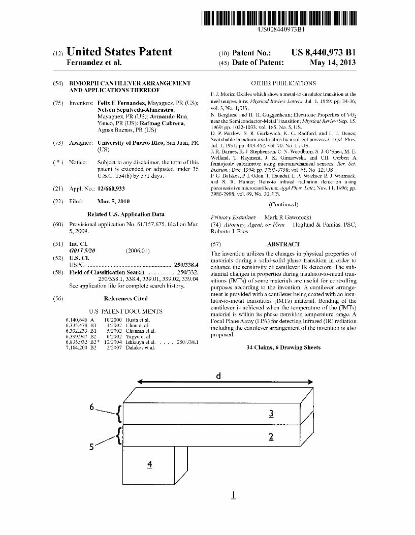
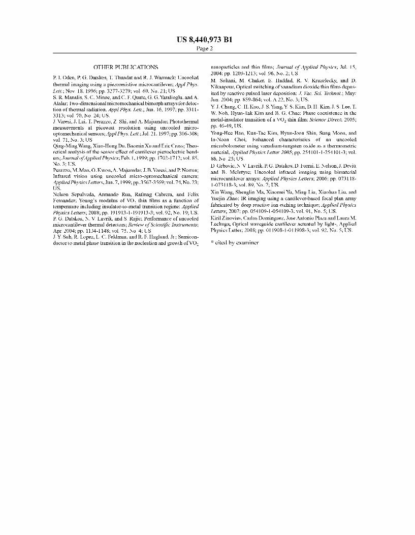
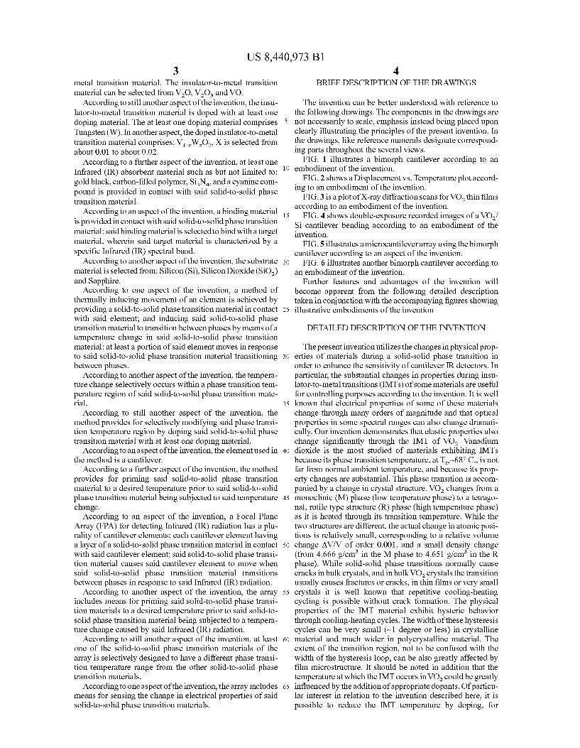
FIG. 1 illustrates a bimorph cantilever according to an embodiment of the invention.
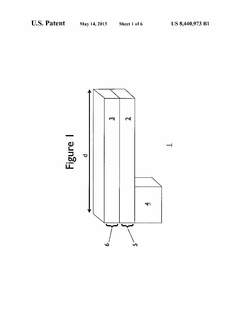
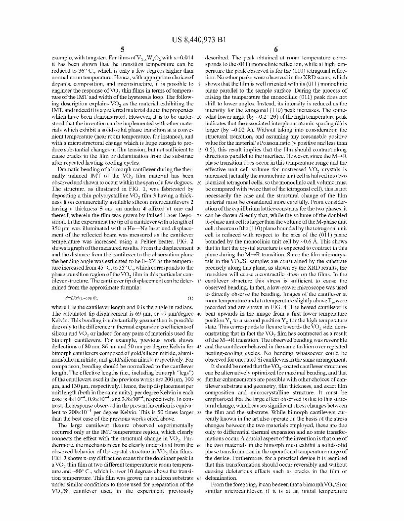
FIG. 2 shows a Displacement vs. Temperature plot accord ing to an embodiment of the invention.
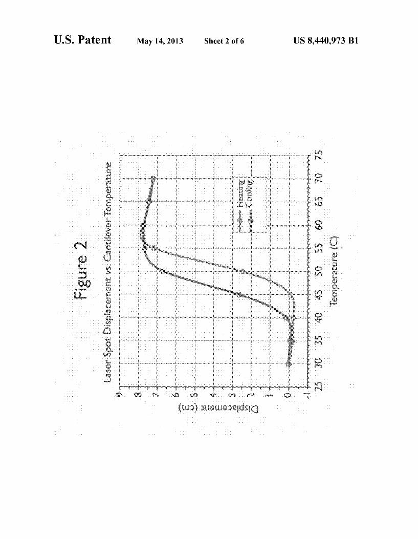
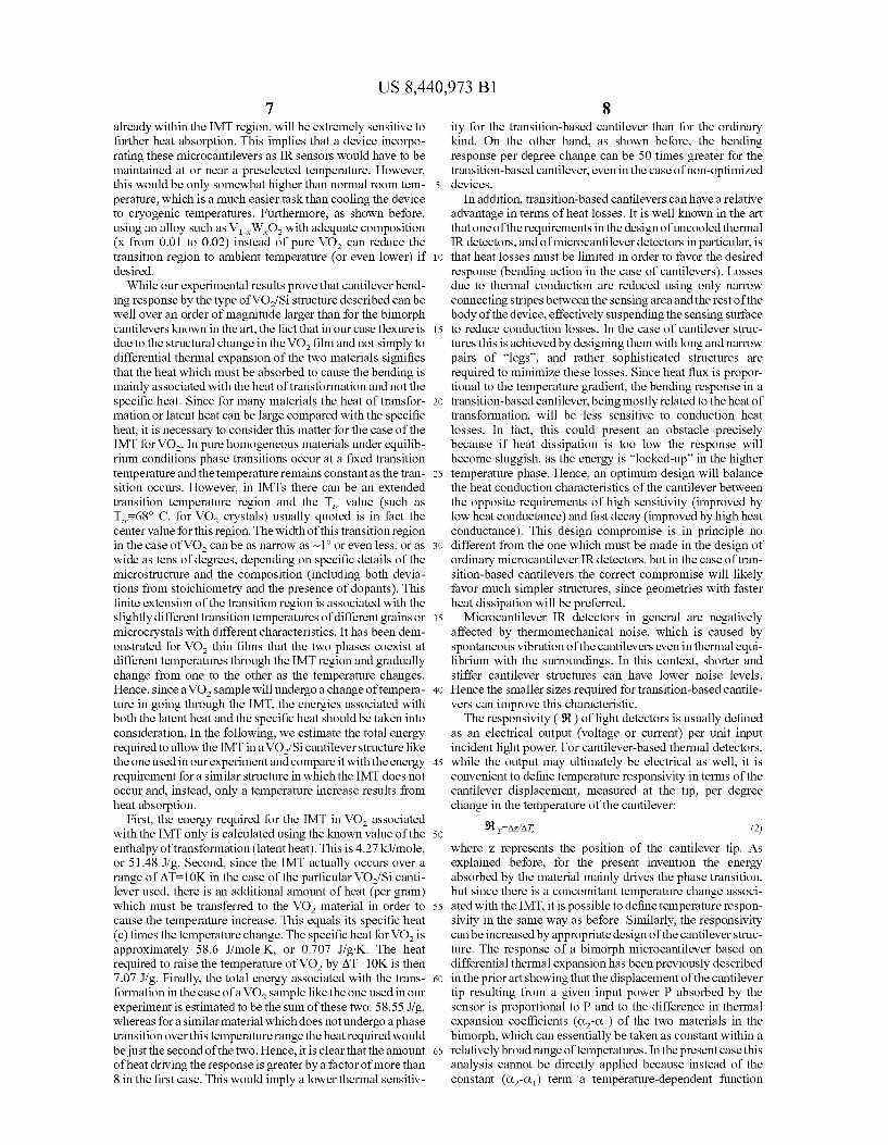
FIG.3 is a plot of X-ray diffraction scans for VO, thin films according to an embodiment of the invention.
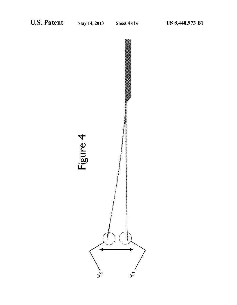
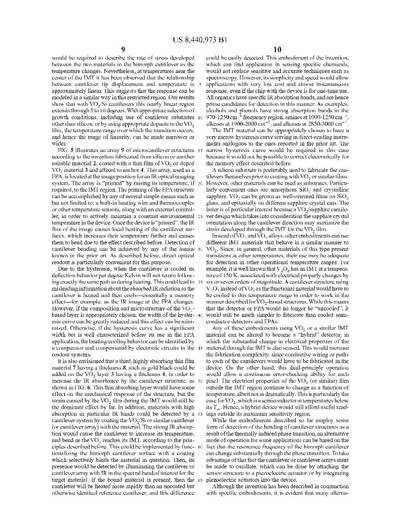
FIG. 4 shows double-exposure recorded images of a VO/ Si cantilever bending according to an embodiment of the invention.
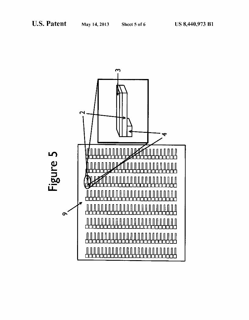
FIG.5 illustrates a microcantilever array using the bimorph cantilever according to an aspect of the invention.
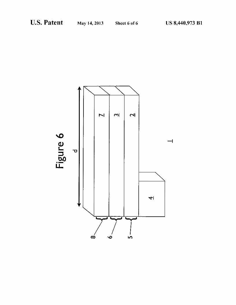
FIG. 6 illustrates another bimorph cantilever according to an embodiment of the invention.
Further features and advantages of the invention will become apparent from the following detailed description taken in conjunction with the accompanying figures showing illustrative embodiments of the invention
DETAILED DESCRIPTION OF THE INVENTION
The present invention utilizes the changes in physical prop erties of materials during a solid-solid phase transition in order to enhance the sensitivity of cantilever IR detectors. In particular, the substantial changes in properties during insu lator-to-metal transitions (IMTs) of some materials are useful for controlling purposes according to the invention. It is well known that electrical properties of some of these materials change through many orders of magnitude and that optical properties in some spectral ranges can also change dramati cally. Our invention demonstrates that elastic properties also change significantly through the IMT of VO. Vanadium dioxide is the most studied of materials exhibiting IMTs because its phase transition temperature, at T-68°C., is not far from normal ambient temperature, and because its prop erty changes are substantial. This phase transition is accom panied by a change in crystal structure. VO changes from a monoclinic (M) phase (low temperature phase) to a tetrago nal, rutile type structure (R) phase (high temperature phase) as it is heated through its transition temperature. While the two structures are different, the actual change in atomic posi tions is relatively small, corresponding to a relative Volume change AV/V of order 0.001, and a small density change (from 4.666 g/cm in the M phase to 4.651 g/cm in the R phase). While solid-solid phase transitions normally cause cracks in bulk crystals, and in bulkVO crystals the transition usually causes fractures or cracks, in thin films or very small crystals it is well known that repetitive cooling-heating cycling is possible without crack formation. The physical properties of the IMT material exhibit hysteric behavior through cooling-heating cycles. The width of these hysteresis cycles can be very Small (~1 degree or less) in crystalline material and much wider in polycrystalline material. The extent of the transition region, not to be confused with the width of the hysteresis loop, can be also greatly affected by film microstructure. It should be noted in addition that the temperature at which the IMT occurs in VO could be greatly influenced by the addition of appropriate dopants. Of particu lar interest in relation to the invention described here, it is possible to reduce the IMT temperature by doping, for
US 8,440,973 B1 5
example, with tungsten. For films of VWO with x=0.014 it has been shown that the transition temperature can be reduced to 36°C., which is only a few degrees higher than normal room temperature. Hence, with appropriate choice of dopants, composition, and microstructure, it is possible to engineer the response of VO, thin films in terms oftempera ture of the IMT and width of the hysteresis loop. The follow ing description explains VO as the material exhibiting the IMT, and indeed it is a preferred material due to the properties which have been demonstrated. However, it is to be under stood that the invention can be implemented with other mate rials which exhibit a solid-solid phase transition at a conve nient temperature (near room temperature, for instance), and with a microstructural change which is large enough to pro duce Substantial changes in film tension, but not sufficient to cause cracks in the film or delamination from the Substrate after repeated heating-cooling cycles.
Dramatic bending of a bimorph cantilever during the ther mally induced IMT of the VO film material has been observed and shown to occur within the span of a few degrees. The structure, as illustrated in FIG. 1, was fabricated by depositing a thin polycrystalline VO film 3 having a thick ness 6 on commercially available silicon microcantilevers 2 having a thickness 5 and an anchor 4 affixed at one end thereof, wherein the film was grown by Pulsed Laser Depo sition. In the experiment the tip of a cantilever with a length of 350 um was illuminated with a He—Ne laser and displace ment of the reflected beam was measured as the cantilever temperature was increased using a Peltier heater. FIG. 2 shows agraph of the measured results. From the displacement and the distance from the cantilever to the observation plane the bending angle was estimated to be 0-23 as the tempera ture increased from 45° C. to 55°C., which corresponds to the phase transition region of the VO film in this particular can tilever structure. The cantilever tip displacement can be deter mined from the approximate formula:
d=L/0* (1-cos 0), (1)
where L is the cantilever length and 0 is the angle in radians. The calculated tip displacement is 69 um, or ~7 um/degree Kelvin. This bending is substantially greater than is possible due only to the difference in thermal expansion coefficients of silicon and VO, or indeed for any pairs of materials used for bimorph cantilevers. For example, previous work shows deflections of 80 nm, 86 nm and 50 nm per degree Kelvin for bimorph cantilevers composed of gold/silicon nitride, alumi num/silicon nitride, and gold/silicon nitride respectively. For comparison, bending should be normalized to the cantilever length. The effective lengths (i.e., including bimorph “legs) of the cantilevers used in the previous works are 200 um, 100 um, and 130 um, respectively. Hence, the tip displacement per unit length (both in the same units), per degree Kelvin in each case is 4x10, 0.9x10", and 3.8x10", respectively. In con trast, the response observed in the present invention is equiva lent to 200x10" per degree Kelvin. This is 50 times larger than the best case of the previous works cited above.
The large cantilever flexure observed experimentally occurred only at the IMT temperature region, which clearly connects the effect with the structural change in VO. Fur thermore, the mechanism can be clearly understood from the observed behavior of the crystal structure in VO, thin films. FIG.3 shows X-ray diffraction scans for the dominant peak in aVO, thin film at two different temperatures: room tempera ture and ~80°C., which is over 10 degrees above the transi tion temperature. This film was grown on a silicon Substrate under similar conditions to those used for preparation of the VO/Si cantilever used in the experiment previously
5
10
15
25
30
35
40
45
50
55
60
65
6 described. The peak obtained at room temperature corre sponds to the (011) monoclinic reflection, while at high tem perature the peak observed is for the (110) tetragonal reflec tion. No other peaks were observed in the XRD scans, which shows that the film is well oriented with its (011) monoclinic plane parallel to the sample Surface. During the process of raising the temperature the monoclinic (011) peak does not shift to lower angles. Instead, its intensity is reduced as the intensity for the tetragonal (110) peak increases. The some what lower angle (by -0.220) of the high temperature peak indicates that the associated interplanar atomic spacing (d) is larger (by ~0.02 A). Without taking into consideration the structural transition, and assuming any reasonable positive value for the materials Poisson ratio (v positive and less than 0.5), this result implies that the film should contract along directions parallel to the interface. However, since the M->R phase transition does occur in this temperature range and the effective unit cell volume for unstressed VO crystals is increased (actually the monoclinic unit cell is halved into two identical tetragonal cells, so the monoclinic cell Volume must be compared with twice that of the tetragonal cell), this is not necessarily the case and the structural change of the film material must be considered more carefully. From consider ation of the equilibrium lattice constants for the two phases, it can be shown directly that, while the volume of the doubled R-phase unit cell is larger than the volume of the M-phase unit cell, the area of the (110) plane bounded by the tetragonal unit cell is reduced with respect to the area of the (011) plane bounded by the monoclinic unit cell by ~0.6 A. This shows that in fact the crystal structure is expected to contract in this plane during the M->R transition. Since the film microcrys tals in the VO/Si samples are constrained by the substrate precisely along this plane, as shown by the XRD results, the transition will cause a contractile stress on the films. In the cantilever structure this stress is sufficient to cause the observed bending. In fact, a low-power microscope was used to directly observe the bending. Images of the cantilever at room temperature and at a temperature slightly above Twere recorded and are shown in FIG. 4. The heated cantilever is bent upwards in the image from a first lower temperature position Y to a second position Y for the high temperature state. This corresponds to flexure towards the VO, side, dem onstrating that in fact the VO film has contracted as a result of the M->R transition. The observed bending was reversible and the cantilever behaved in the same fashion over repeated heating-cooling cycles. No bending whatsoever could be observed for uncoated Sicantilevers in the same arrangement.
It should be noted that the VO-coated cantilever structures can be alternatively optimized for maximal bending, and that further enhancements are possible with other choices of can tilever Substrate and geometry, film thickness, and exact film composition and microcrystalline structure. It must be emphasized that the large effect observed is due to this struc tural change, which causes significant stress changes between the film and the substrate. While bimorph cantilevers cur rently known in the art also operate on the basis of the stress changes between the two materials employed, these are due only to differential thermal expansion and no state transfor mations occur. A crucial aspect of the invention is that one of the two materials in the bimorph must exhibit a solid-solid phase transformation in the operational temperature range of the device. Furthermore, for a practical device it is required that this transformation should occur reversibly and without causing deleterious effects such as cracks in the film or delamination. From the foregoing, it can be seen that a bimorphVO/Sior
similar microcantilever, if it is at an initial temperature
US 8,440,973 B1 7
already within the IMT region, will be extremely sensitive to further heat absorption. This implies that a device incorpo rating these microcantilevers as IR sensors would have to be maintained at or near a preselected temperature. However, this would be only somewhat higher than normal room tem perature, which is a much easier task than cooling the device to cryogenic temperatures. Furthermore, as shown before, using an alloy Such as VWO with adequate composition (x from 0.01 to 0.02) instead of pure VO, can reduce the transition region to ambient temperature (or even lower) if desired.
While our experimental results prove that cantilever bend ing response by the type of VO/Si structure described can be well over an order of magnitude larger than for the bimorph cantilevers known in the art, the fact that in our case flexure is due to the structural change in the VO film and not simply to differential thermal expansion of the two materials signifies that the heat which must be absorbed to cause the bending is mainly associated with the heat of transformation and not the specific heat. Since for many materials the heat of transfor mation or latent heat can be large compared with the specific heat, it is necessary to consider this matter for the case of the IMT for VO. In pure homogeneous materials under equilib rium conditions phase transitions occur at a fixed transition temperature and the temperature remains constant as the tran sition occurs. However, in IMTs there can be an extended transition temperature region and the T value (Such as T-68° C. for VO, crystals) usually quoted is in fact the center value for this region. The width of this transition region in the case of VO can be as narrow as ~1° or even less, or as wide as tens of degrees, depending on specific details of the microstructure and the composition (including both devia tions from Stoichiometry and the presence of dopants). This finite extension of the transition region is associated with the slightly different transition temperatures of different grains or microcrystals with different characteristics. It has been dem onstrated for VO, thin films that the two phases coexist at different temperatures through the IMT region and gradually change from one to the other as the temperature changes. Hence, since a VO. sample will undergo a change oftempera ture in going through the IMT, the energies associated with both the latent heat and the specific heat should be taken into consideration. In the following, we estimate the total energy required to allow the IMT in a VO/Sicantilever structure like the one used in our experiment and compare it with the energy requirement for a similar structure in which the IMT does not occur and, instead, only a temperature increase results from heat absorption.
First, the energy required for the IMT in VO, associated with the IMT only is calculated using the known value of the enthalpy of transformation (latent heat). This is 4.27 kJ/mole, or 51.48 J/g. Second, since the IMT actually occurs over a range of AT=10K in the case of the particular VO/Si canti lever used, there is an additional amount of heat (per gram) which must be transferred to the VO, material in order to cause the temperature increase. This equals its specific heat (c) times the temperature change. The specific heat for VO is approximately 58.6 J/mole K, or 0.707 J/g-K. The heat required to raise the temperature of VO, by AT=10K is then 7.07 J/g. Finally, the total energy associated with the trans formation in the case of a VO, sample like the one used in our experiment is estimated to be the sum of these two: 58.55 J/g, whereas for a similar material which does not undergo a phase transition over this temperature range the heatrequired would be just the second of the two. Hence, it is clear that the amount of heat driving the response is greater by a factor of more than 8 in the first case. This would imply a lower thermal sensitiv
10
15
25
30
35
40
45
50
55
60
65
8 ity for the transition-based cantilever than for the ordinary kind. On the other hand, as shown before, the bending response per degree change can be 50 times greater for the transition-based cantilever, even in the case of non-optimized devices.
In addition, transition-based cantilevers can have a relative advantage in terms of heat losses. It is well known in the art that one of the requirements in the design of uncooled thermal IR detectors, and of microcantilever detectors in particular, is that heat losses must be limited in order to favor the desired response (bending action in the case of cantilevers). Losses due to thermal conduction are reduced using only narrow connecting stripes between the sensing area and the rest of the body of the device, effectively Suspending the sensing Surface to reduce conduction losses. In the case of cantilever struc tures this is achieved by designing them with long and narrow pairs of "legs, and rather Sophisticated structures are required to minimize these losses. Since heat flux is propor tional to the temperature gradient, the bending response in a transition-based cantilever, being mostly related to the heat of transformation, will be less sensitive to conduction heat losses. In fact, this could present an obstacle precisely because if heat dissipation is too low the response will become sluggish, as the energy is "locked-up' in the higher temperature phase. Hence, an optimum design will balance the heat conduction characteristics of the cantilever between the opposite requirements of high sensitivity (improved by low heat conductance) and fast decay (improved by high heat conductance). This design compromise is in principle no different from the one which must be made in the design of ordinary microcantilever IR detectors, but in the case of tran sition-based cantilevers the correct compromise will likely favor much simpler structures, since geometries with faster heat dissipation will be preferred.
Microcantilever IR detectors in general are negatively affected by thermomechanical noise, which is caused by spontaneous vibration of the cantilevers even in thermal equi librium with the surroundings. In this context, shorter and stiffer cantilever structures can have lower noise levels. Hence the smaller sizes required for transition-based cantile vers can improve this characteristic. The responsivity (9) of light detectors is usually defined
as an electrical output (voltage or current) per unit input incident light power. For cantilever-based thermal detectors, while the output may ultimately be electrical as well, it is convenient to define temperature responsivity in terms of the cantilever displacement, measured at the tip, per degree change in the temperature of the cantilever:
9 =Az/AT, (2) where Z represents the position of the cantilever tip. As explained before, for the present invention the energy absorbed by the material mainly drives the phase transition, but since there is a concomitant temperature change associ ated with the IMT, it is possible to define temperature respon sivity in the same way as before. Similarly, the responsivity can be increased by appropriate design of the cantilever struc ture. The response of a bimorph microcantilever based on differential thermal expansion has been previously described in the prior art showing that the displacement of the cantilever tip resulting from a given input power P absorbed by the sensor is proportional to P and to the difference in thermal expansion coefficients (C-C) of the two materials in the bimorph, which can essentially be taken as constant within a relatively broad range oftemperatures. In the present case this analysis cannot be directly applied because instead of the constant (C-C) term a temperature-dependent function
US 8,440,973 B1 9
would be required to describe the rate of stress developed between the two materials in the bimorph cantilever as the temperature changes. Nevertheless, at temperatures near the center of the IMT it has been observed that the relationship between cantilever tip displacement and temperature is approximately linear. This suggests that the response can be modeled in a similar way in this restricted region. Our results show that with VO/Si cantilevers this nearly linear region extends through 5 to 10 degrees. With appropriate selection of growth conditions, including use of cantilever Substrates other than silicon, or by using appropriate dopants in the VO film, the temperature range over which the transition occurs, and hence the range of linearity, can be made narrower or wider.
FIG. 5 illustrates an array 9 of microcantilever structures according to the invention fabricated from silicon or another suitable material 2, coated with a thin film of VO, or doped VO material 3 and affixed to anchor 4. This array, used as a FPA, is located at the image position for an IR optical imaging system. The array is “primed by raising its temperature, if required, to the IMT region. The priming of the FPA structure can be accomplished by any of several simple means such as but not limited to: a built-in heating wire and thermocouples or other temperature sensors, along with an external control ler, in order to actively maintain a constant environmental temperature in the device. Once the device is “primed, the IR flux of the image causes local heating of the cantilever Sur faces, which increases their temperature further and causes them to bend due to the effect described before. Detection of cantilever bending can be achieved by any of the means known in the prior art. As described before, direct optical readout is particularly convenient for this purpose. Due to the hysteresis, when the cantilever is cooled its
deflection behavior per degree Kelvin will not return follow ing exactly the same path as during heating. This could lead to misleading information about the absorbed IR radiation as the cantilever is heated and then cools—essentially a memory effect—for example, as the IR image at the FPA changes. However, if the composition and microstructure of the VO based layer is appropriately chosen, the width of the hyster esis curve can be greatly reduced and this effect can be mini mized. Otherwise, if the hysteresis curve has a significant width but is well characterized before its use in the FPA application, the heating/cooling behavior can be identified by a comparator and compensated by electronic circuits in the readout systems.
It is also envisioned that a third, highly absorbing thin film material 7 having a thickness 8, such as gold black could be added on the VO layer 3 having a thickness 6, in order to increase the IR absorbance by the cantilever structure, as shown in FIG. 6. This thin absorbing layer would have some effect on the mechanical response of the structure, but the strain caused by the VO film during the IMT would still be the dominant effect by far. In addition, materials with high absorption in particular IR bands could be detected by a cantilever system by coating the VO/Sior similar cantilever (or cantilever array) with the material. The strong IR absorp tion would cause the cantilever to increase its temperature, and bend as the VO, reaches its IMT, according to the prin ciples described before. This could be implemented by func tionalizing the bimorph cantilever Surface with a coating which selectively binds the material in question. Then, its presence would be detected by illuminating the cantilever or cantilever array with IR in the spectral band of interest for the target material. If the bound material is present, then the cantilever will be heated more rapidly than an uncoated but otherwise identical reference cantilever, and this difference
10
15
25
30
35
40
45
50
55
60
65
10 could be easily detected. This embodiment of the invention, which can find application in sensing specific chemicals, would not replace sensitive and accurate techniques such as spectroscopy. However, its simplicity and speed would allow applications with very low cost and almost instantaneous response, even if the chip with the device is for one-time use. All organics have specific IR absorption bands, and are hence prime candidates for detection in this manner. As examples, alcohols and phenols have strong absorption bands in the 970-1250 cm frequency region, amines at 1000-1250 cm', alkenes at 1900-2000 cm, and alkanes at 2850-3000 cm. The IMT material can be appropriately chosen to have a
very narrow hysteresis curve serving in direct-reading instru ments analogous to the ones reported in the prior art. The narrow hysteresis curve would be required in this case because it would not be possible to correct electronically for the memory effect described before. A silicon substrate is preferably used to fabricate the can
tilevers themselves prior to coating with VO or similar films. However, other materials can be used as substrates. Particu larly convenient ones are amorphous SiO, and crystalline sapphire. VO can be grown as well-oriented films on SiO, glass, and epitaxially on different Sapphire crystal cuts. The latter is of particular interest because a VO/sapphire cantile Verdesign which takes into consideration the Sapphire crystal orientation along the cantilever direction may maximize the strain developed through the IMT for the VO film.
Instead of VO, andVO, alloys, other embodiments can use different IMT materials that behave in a similar manner to VO. Since, in general, other materials of this type present transitions at other temperatures, their use may be adequate for detection in other operational temperature ranges. For example, it is well known that V.O., has an IMT at a tempera ture of 150 K, associated with electrical property changes by six or seven orders of magnitude. A cantilever structure using VO instead of VO as the functional material would have to be cooled to this temperature range in order to work in the manner described for VO-based structures. While this means that the detector or FPA would no longer be “uncooled, it would still be much simpler to fabricate than cooled semi conductor detectors and FPAs. Any of these embodiments using VO, or a similar IMT
material can be altered to become a “hybrid detector, in which the substantial change in electrical properties of the material through the IMT is also sensed. This would increase the fabrication complexity, since conductive wiring or paths to each of the cantilevers would have to be fabricated in the device. On the other hand, this dual-principle operation would allow a continuous error-checking ability for each pixel. The electrical properties of the VO (or similar) film outside the IMT region continue to change as a function of temperature, albeit not as dramatically. This is particularly the case for VO, which is a semiconductor attemperatures below its T. Hence, a hybrid device would still afford useful read ings outside its maximum sensitivity region.
While the embodiments described so far employ some form of detection of the bending of cantilever structures as a result of the thermally induced phase transition, an alternative mode of operation for Some applications can be based on the fact that the resonance frequency of the bimorph cantilever can change substantially through the phase transition. To take advantage of this fact the cantilever or cantilever arrays must be made to oscillate, which can be done by attaching the sensor structure to a piezoelectric actuator or by integrating piezoelectric actuators into the device.
Although the invention has been described in conjunction with specific embodiments, it is evident that many alterna
US 8,440,973 B1 11
tives and variations will be apparent to those skilled in the art in light of the foregoing description. Accordingly, the inven tion is intended to embrace all of the alternatives and varia tions that fall within the spirit and scope of the appended claims. We claim: 1. A thermally-induced moving assembly comprising: a substrate material; a solid-to-solid phase transition material in contact with
said substrate material, wherein said solid-to-solid phase transition material causes at least a portion of said Substrate material to move when subjected to a tempera ture change.
2. The assembly of claim 1, wherein said solid-to-solid phase transition material comprises an insulator-to-metal transition material.
3. The assembly of claim 2, wherein said insulator-to-metal transition material is selected from the group consisting of VO, and VO.
4. The assembly of claim 2, wherein said insulator-to-metal transition material comprises: VO.
5. The assembly of claim 1, wherein said insulator-to-metal transition material is doped with at least one doping material.
6. The assembly of claim 5, wherein said at least one doping material comprises Tungsten (W).
7. The assembly of claim 5, wherein said doped insulator to-metal transition material comprises: V.W.O.; X is selected from about 0.01 to about 0.02.
8. The assembly of claim 1, further comprising at least one Infrared (IR) absorbent material in contact with said solid-to Solid phase transition material.
9. The assembly of claim 8, wherein said at least one (IR) absorbent material comprises at least one of gold black, carbon-filled polymer, SiNa, and cyanine compound.
10. The assembly of claim 1, further comprising a binding material in contact with said solid-to-solid phase transition material; said binding material is selected to bind with a target material, wherein said target material is characterized by a specific Infrared (IR) spectral band.
11. The assembly of claim 1, wherein said substrate mate rial is selected from the group consisting of Silicon (Si), Silicon Dioxide (SiO) and Sapphire.
12. A method of thermally inducing movement of an ele ment comprising:
providing a solid-to-solid phase-transition material in con tact with said element; and
inducing said solid-to-solid phase transition material to transition between phases by means of a temperature change in said solid-to-solid phase transition material;
at least a portion of said element moves in response to said Solid-to-solid phase transition material transitioning between phases.
13. The method of claim 12, wherein said temperature change selectively occurs within a phase transition tempera ture region of said solid-to-solid phase transition material.
14. The method of claim 13, further comprising selectively modifying said phase transition temperature region.
15. The method of claim 14, wherein said phase transition temperature region is modified by doping said solid-to-solid phase transition material with at least one doping material.
16. The method of claim 15, wherein said at least one doping material comprises Tungsten (W).
5
10
15
25
30
35
40
45
50
55
60
12 17. The method of claim 16, wherein said doped insulator
to-metal transition material comprises: V.W.O.; X is selected from about 0.01 to about 0.02.
18. The method of claim 12, wherein said solid-to-solid phase transition material comprises an insulator-to-metal transition material.
19. The method of claim 18, wherein said insulator-to metal transition material is selected from the group consisting of VO and VO.
20. The method of claim 18, wherein said insulator-to metal transition material comprises: VO.
21. The method of claim 12, wherein said element is made from a material selected from the group consisting of Silicon (Si), Silicon Dioxide (SiO2) and Sapphire.
22. The method of claim 12, wherein said element com prises a cantilever.
23. The method of claim 12, further comprising: priming said solid-to-solid phase transition material to a
desired temperature prior to said solid-to-solid phase transition material being subjected to said temperature change.
24. A Focal Plane Array (FPA) for detecting Infrared (IR) radiation comprising:
a plurality of cantilever elements; each cantilever element having a layer of a solid-to-solid
phase transition material in contact with said cantilever element; said solid-to-solid phase transition material causes said cantilever element to move when said solid to-solid phase transition material transitions between phases in response to said Infrared (IR) radiation.
25. The array of claim 24, further comprising: means for priming said solid-to-solid phase transition
materials to a desired temperature prior to said solid-to Solid phase transition material being subjected to a tem perature change caused by said Infrared (IR) radiation.
26. The array of claim 24, wherein said solid-to-solid phase transition materials comprise an insulator-to-metal transition material.
27. The array of claim 26, wherein said insulator-to-metal transition material is selected from the group consisting of: VO, and VO.
28. The array of claim 26, wherein said insulator-to-metal transition material comprises: VO.
29. The array of claim 26, wherein said insulator-to-metal transition material is doped with at least one doping material.
30. The array of claim 29, wherein said at least one doping material comprises Tungsten (W).
31. The array of claim 30, wherein said doped insulator to-metal transition material comprises: V.W.O.; X is selected from about 0.01 to about 0.02.
32. The array of claim 24, wherein said plurality of canti lever elements is made from a material selected from the group consisting of Silicon (Si), Silicon Dioxide (SiO) and Sapphire.
33. The array of claim 24, wherein at least one of said Solid-to-solid phase transition materials is selectively designed to have a different phase transition temperature range from the other solid-to-solid phase transition materials.
34. The array of claim 24, further comprising: means for sensing the change in electrical properties of
said solid-to-solid phase transition materials. ck ck ck ck ck