Embed Size (px)
Citation preview

US008811039B2
(12) Un1ted States Patent (10) Patent No.: US 8,811,039 B2
The N 0 et al. 45 Date of Patent: Au . 19 2014a
(54) PULSE WIDTH MODULATED RESONANT 2008/0055942 A1 * 3/2008 Tao et a1. ................... 363/2103
POWER CONVERSION 2008/0186742 A1* 8/2008 Seong ........... 363/17
2009/0303750 A1 * 12/2009 Zhu et al. ..... 363/13
. 2010/0142229 A1 * 6/2010 Chen et al. ...... 363/2102
(75) Inventors: Khal Dean The Ngo, Blacksburg, YA 2010/0254163 A1* 10/2010 Martini et 31. .. ........ 363/17
(US); Xlao C30, Itasca, IL (US); Yln 2011/0090717 A1* 4/2011 Lee et al. ................... 363/2102
Wan , Blacksbur , VA S
g g (U ) OTHER PUBLICATIONS
(73) ASSlgnee: Ezglgizcrf<2$jlfign$£e$llsjl Propertles, A. K. Jain et al.; “PWM Control ofDual Active Bridge: Comprehen-
I’ g’ sive Analysis and Experimental Verification”; Industrial Electronics,
( * ) Notice: Subject to any disclaimer, the term ofthis :ggfgiCON 2008,34thAnnual Conference ofIEEE, Nov. 2008,pp.
pJatSerét 11$5:331:3(1632721‘dadJuSted under 35 Xuaodong Li et al.; “Analysis and Design of High-Frequency Iso-
' ' ' y ays. lated Dual-Bridge Series Resonant DC/DC Converter”; IEEE Trans-
(21) Appl No . 13/184 798 actions on Power Electronics, vol. 25, No. 4, Apr. 2010, pp. 850-862.
. .. ,
* 't d b '
(22) Filed: Jul. 18, 2011 Cl e y exammer
_ _ _ Primary Examiner 7 Adolf Berhane
(65) Prlor Publlcatlon Data Assistant Examiner 7 Fred E Finch, III
US 2012/0014138 A1 Jan. 19, 2012 (74) Attorney, Agent, or Firm 7 Whitham, Curtis,
Chr‘istofferson & Cook, P.C.
Related US. Application Data
(60) Provisional application No. 61/364,954, filed on Jul. (57) ABSTRACT
16, 2010. A ower converter includin a resonant circuit is controlledP g
by pulse width modulation (PWM) of a switching circuit to
(51) Int. Cl- control current in the resonant circuit near the frequency of
H02M3/335 (2006.01) the resonant circuit (a null-immittance criterion) in order to
(52) US. Cl. control current and voltage at the output of the resonant
USPC .......................................... 363/21.02; 363/98 circuit. Further control ofvoltage can be performed by PWM
(58) Field of Classification Search ofa switching circuit at the output ofthe resonant circuit such
USPC ........................ 363/17, 210172103, 98, 132 that centers of the duty cycles of reSpective switches for the
See application file for complete search history. output of the resonant circuit are substantially synchronized
and substantially symmetrical about centers of said duty
(56) References Cited cycles of respective switches at the input of the resonant
U.S. PATENT DOCUMENTS
6,151,222 A * 11/2000 Barrett ............................ 363/16
2006/0187686 A1* 8/2006 Sun et al. ...... 363/17
2007/0041222 A1* 2/2007 Eguchi et al. 363/17
2007/0070655 A1* 3/2007 Eguchi et al. ................... 363/17
circuit. Thus, operation of the converter is substantially sim-
plified by using only PWM, a wide range of input and output
voltages can be achieved and the converter circuit can be
configured for bi-directional power transfer.
17 Claims, 17 Drawing Sheets
PWM
Battery Vch

120
SystemDiagram
100
D1?
D2;
110
93
"K“D41
13f
1‘?
15\U
5
Motor160
DC—DC
Batte
DC~AC
g
Converter
ry
inverter
{fl
02%
Figure
1
U.S. Patent Aug. 19, 2014 Sheet 1 of 17 US 8,811,039 B2

Battery
V1102
+
AC—DC
Rectifier
Vdc1
I
I
Figure2
(RelatedArt)
Phase—ShiftingModulation
Phase-ShiftingModulation
Phase—Shifting+PWM
Modulatior
VVp
V5
V8
Vp
_.0
Vs
(p>0
LP<O
—
Figure3A
Figure3B
Figure30
(RelatedArt)
(RelatedArt)
(RelatedArt)
U.S. Patent Aug. 19, 2014 Sheet 2 of 17 US 8,811,039 B2

p1
3132
331
3
AC-DC
Rectifier
Vdc1
8.01,
32K
0Cr
Lr
tl
+
+H
IO
+
Vp
VS
Co::
Battery
Vdc2
52’K
sp2'
39k
s
./._____,/.
Figure4
(RelatedArt)
AVS
oL/‘g
t\_7
Figure5
{RelatedArt)
U.S. Patent Aug. 19, 2014 Sheet 3 of 17 US 8,811,039 B2

U.S. Patent Aug. 19, 2014
+ VS
Co::
Battery
Figure6
Sheet 4 of 17 US 8,811,039 B2

TVbridgein
+l
E
Vout
U.S. Patent Aug. 19, 2014 Sheet 5 of 17 US 8,811,039 B2

Figure 6B
Gate Driver Signai
Geneiator Biock
PWM Generator Block
V4
1
U3
L
U1
.55" ""x
TV3
Vbout1
%V7
£5“—
[YE
Vb:n_legZ
U18
T;
Q
33'?
TJ'
QN
Vbout
1992
U16
U7
35
Li:
J;
U15
D33
U.S. Patent Aug. 19, 2014 Sheet 6 of 17 US 8,811,039 B2

US. Patent Aug. 19, 2014 Sheet 7 of 17 US 8,811,039 B2
__| \J\> L g
/// 7
< a,\ or:
T \\>
/
36
/\
—L_....._:—“—L____l—_~'1
I
/‘\
\/
\//
\/
34 FigureBC
\ \> I
l-D‘Zf'va-OWCONFCD WMNi—C) 'd‘C‘ONR-“O ‘ETCQNv-Cj
Vbin‘l
I
Vbin1_leg1
Vbin‘lmlegZ
l
A Amie mm mm Awda> K
:3
C)
(D
U‘)
"U
'E
.D
>

US. Patent Aug. 19, 2014 Sheet 8 of 17 US 8,811,039 B2
\\ I 9*
>
// '
/
< 5%
_. \\
\>/
—_L___F—I___..._I———_I
/
x/
\/
\/
\/
FigureGD
‘</ E
\\
\>.._. / N
<//
\
\
\
Lf)<:'UJNPO'<§‘<‘0C\WC) VODNPO fi'C'JNFO "fi'mmx—CD
100
50 G
-50
400
Vhoufl
|
Vbout1jeg1
VboutLEegZ
i
/
V
:5
OA l 95PIJQA A A/LSG A/ZSCI MESG A/VSU._.__

US. Patent Aug. 19, 2014 Sheet 9 of 17 US 8,811,039 B2
Gate
Signal 1
0 1‘
Gate ;
SignaE 2 8132 ..
0 t
V V'nuuuuuu Vp
dc1 V
V - 53C102 5
0 ‘—"§ '1‘
I
Figure 7

US. Patent Aug. 19, 2014 Sheet 10 of 17 US 8,811,039 B2
c I gr LI 1' +
+ I - +
@Vdm Vp g 3 Vs 00:: Battery Vdc2
Time (us)
Figure 8

US. Patent Aug. 19, 2014 Sheet 11 of 17 US 8,811,039 B2
500
250
IL(A)
-250
-500
500
400
300
Vdc2
(V)
200
100

US 8,811,039 B2Sheet 12 of 17Aug. 19, 2014U.S. Patent
(9MB
WA
(mugs
———w-—
_
(mugs
809A
:3!ugeBafienoneqi
A“
0LamfiH
3353A
LOPA
{A

US. Patent Aug. 19, 2014 Sheet 13 of 17 US 8,811,039 B2
4.5
4 — 10% Load
3 5 +50% Load
1:: '3 + Full Load
'3 + Caiculaied
O 2.5
G.)
E 2
g 1.5
1
0.5
O
0 20 4O 60 80 100
l3 2 (°)
4 m U
35 (1‘50 —10% Load
‘3 +50% Load
E + Full Load
8 2'5 + Calculated
m 2
0')
$1 5
>0 1
0.5
O I I I I
20 40 60 80 100
l3 5 (°)
2.5
a = 30° m 10% Load
2 + 50% Load
C \ W Full Load
'- a... Calculated33 1.5 ’\
CD
a \\
E 1 \0.5
O I I E I 100
{35 (°)
Figure 11

US. Patent Aug. 19, 2014 Sheet 14 of 17 US 8,811,039 B2
Waveforms of Resonant Current and Vds of MOSFET
40.0 . . .
30.0-
20.0-
10,0-
~100-
-20.0-
-30.0-
-40.0
40.0
30.0-
20.0-
10.0-
0.
-1 0.0-
-20.0—
-30.0- : : : :~40.0 ' ‘ - - v
40.0 . . .
30.0-
20.0-
10.0-
o.
-1 0.0--
-20.0-
~300-
40.0
40.0
30.0-
20.0-
10.0-
0.
40.0--
~200-
00.0-
-40.0 E
2900 292u
SwitchingFrequency:219kHz
SwitchingFrequency:240kHz
2041: 290a 2911; 300:;
its)
Resonant Frequency: 219 kHz
Figure 12

D33T
034T
Battery
Figure13
Figure14
Battery
Vdc2
Vdc2
U.S. Patent Aug. 19, 2014 Sheet 15 of 17 US 8,811,039 B2
l'lin Jl
II
+
H0
0+-
;g
VCaz:
Battery
Vdc2
Source/
Load
Sp4
Sp5
’Load/
Source
II
1
SPA
354
885
356
I'II
Figure16
U.S. Patent Aug. 19, 2014 Sheet160f17 US 8,811,039 B2

‘l:
Identify
Fm,“atwhich203W“)or
Y(F,,u")of
FilterNetwork=0
2:
At
Fm,”the
FilterNetworkforcesVFm(FnU”)=
V,Out(FnU”)or
1Fm(|=null)=
lmaznuu)
I
input
g.lp
Voltage/
m>
Ingt
km
Fitter
IFOU’E
Output
Iout
Output
+Swatches
+’
Nh
-Volta
/
Current
etwork
+'
SWItches
+93
Yin
[J
YFin
_L
VFW:
JVOUt
Current
Vin
Jfil
TE
'At!
_
tg
lSwitch
inputswitches
at
Fnullwithconductionangle
O(togeneratefundamentalharmonic
VFin(Fnull)=
f(Vin’
0‘)
or
IFin(Fnull)=
3:“id(X)
\l/
Switchoutputswitches
at
Fm,“withconductionangleBtogeneratefundamentalharmonic
V:Fout(F:null)9(V0ut'B)
or
1FOUI(F:‘1UII)=
g(|out'8)
Voltagegain
orcurrentgain
isestablishedbycombiningstems
2,3and
4:
f(Vina):
9(Voet
E?)
OF
f(n‘(IX):
9(lout'B)
Figure17
U.S. Patent Aug. 19, 2014 Sheet 17 of 17 US 8,811,039 B2

US 8,811,039 B2
1
PULSE WIDTH MODULATED RESONANT
POWER CONVERSION
CROSS-REFERENCE TO RELATED
APPLICATIONS
This application claims priority ofUS. Provisional Patent
Application 61/364,954, filed Jul. 16, 2010, which is hereby
incorporated by reference in its entirety.
FIELD OF THE INVENTION
The present invention generally relates to power conver-
sion and power converter circuits such as may be required for
charging batteries of electric vehicles or storing power from
intermittently available sources such as power derived from
renewable resources and, more particularly, to power convert-
ers capable ofcontrolling output voltage through pulse width
modulation.
BACKGROUND OF THE INVENTION
While alternating current (AC) has long been the standard
for distributing power, particularly to loads in fixed locations
that may be widely separated from power generation sources
where power is continuously generated, there is increasing
interest in power systems using so-called renewable
resources such as solar and wind power where power genera-
tion may be intermittent and generated power, when avail-
able, must be stored, often as the potential energy of stored
charge, until needed. The same is true for portable or mobile
devices which must generally contain their own power
sources, such as electrical generators and/or batteries which
store energy as charge and deliver that energy as direct current
(DC). If alternating current is required by the ultimate load,
so-called power inverters can be used to develop AC power
from a DC power input. On the other hand, batteries are often
not an economical source of portable power unless they are
capable of being recharged using energy which is ultimately
generated and distributed as alternating current.
Among applications where the powered device is mobile
and energy must necessarily be intermittently stored, there
has been much recent interest in using electrical power for
powering vehicles in order to avoid or at least reduce atmo-
spheric pollution, particularly in areas where numerous
vehicles are concurrently in use. Therefore, there has been a
corresponding interest in various technologies for batteries
which can store greater quantities of energy in order to
increase the range of the vehicles as well as the capability of
such batteries to be quickly recharged; ideally, within a period
time comparable to that required for filling the fuel tank of a
vehicle powered by an internal combustion engine. Thus,
variable voltage may be necessary for both rapidly charging
batteries and to prolong battery life as well as to accommo-
date various safety concerns encountered in some technolo-
gies. Further, isolation ofthe battery from the power source is
generally desirable, particularly for reasons of safety.
In summary, particularly for charging batteries capable of
storing relatively large amounts of energy, it is generally
desirable to provide an isolated DC-DC converter capable of
operating in either buck or boost mode in order to provide an
output voltage which is variable over a wide range from a
relatively constant input voltage and which is capable of
bi-directional power flow. Both buck and boost modes are
desirable since input voltage may be higher or lower than the
desired output voltage. In the case of battery charging, the
output voltage desired depends ofthe state of battery charge;
10
20
25
40
45
55
2
At he beginning ofbattery charging the voltage could be very
low but near full charge, the voltage is high. Bi-directional
power flow capability is desirable since, in addition to trans-
ferring power from the grid or a local generator to a battery,
the battery may be required to provide energy to the grid or
other devices or to another battery.
It is also generally desirable for the DC-DC converter to be
controllable to produce a variable output voltage in a simple
manner that does not require complex circuitry to produce
suitable control waveforms and which has so-called soft
switching capabilities (e.g. where switching is performed
when voltage and/or current is low or zero) in order to achieve
high efficiency. It is also very desirable for high efficiency to
be maintained over a wide range of load conditions since the
load presented by a battery under charging conditions may be
very large when the battery has been deeply discharged but
may be much smaller as the battery approaches full charge. In
this latter regard, it is also very desirable for the output voltage
of the converter to be controllable in a predictable manner;
requiring that the controlled output voltage to be substantially
unaffected by the load which the battery presents.
Unfortunately, power converter circuits developed prior to
the present invention have not been able to achieve all ofthese
desirable features. In particular, known isolated DC-DC con-
verters capable of bi-directional power flow have only been
capable of providing soft switching over a very narrow load
range and have exhibited load-dependent voltage gain even
when complicated control schemes and circuitry are
employed.
SUMMARY OF THE INVENTION
It is therefore an object of the present invention to provide
a DC-DC power converter capable of supplying a high and
variable voltage at high current in a load-independent manner
using simplified control.
In order to accomplish this and other objects of the inven-
tion, a power converter is provided comprising a first switch-
ing circuit having a plurality of switches, a second switching
circuit having a plurality of switches, a connection between
the first switching circuit and the second switching circuit
including a resonant circuit, and a pulse width modulation
circuit for providing driving pulses to drive the plurality of
switches of at least the first switching circuit at a frequency
near a resonant frequency of the resonant circuit.
In accordance with another aspect of the invention, a
method ofoperating a power converter circuit having first and
second switching circuits, each switching circuit comprising
a plurality of switches connected to provide conversion
betweenAC and DC voltage, and a resonant circuit connect-
ing the first and second switching circuits, the method com-
prising controlling switches of at least the first switching
circuit to provide pulse width modulated current in the reso-
nant circuit at a frequency near a resonant frequency of said
resonant circuit.
BRIEF DESCRIPTION OF THE DRAWINGS
The foregoing and other objects, aspects and advantages
will be better understood from the following detailed descrip-
tion of a preferred embodiment of the invention with refer-
ence to the drawings, in which:
FIG. 1 is a high-level schematic diagram of a system for
supplying power to a motor such as may be provided for an
electric powered vehicle,

US 8,811,039 B2
3
FIG. 2 is a schematic diagram of a portion ofthe system of
FIG. 1 including a known Dual active bridge (DAB) con-
verter,
FIGS. 3A, 3B and 3C are waveforms used to control
amount and direction ofpower transfer in the DAB converter
of FIG. 2,
FIG. 4 is a schematic diagram of a known series resonant
DAB converter,
FIG. 5 illustrates waveforms corresponding to operation of
the series resonant DAB converter of FIG. 4,
FIG. 6 is a schematic diagram of a series resonant DAB
converter in accordance with the invention,
FIG. 6A is a schematic diagram of a preferred main circuit
for producing symmetrical, synchronized PWM waveforms
in accordance with the invention,
FIG. 6B is a schematic diagram of a preferred main circuit
for producing symmetrical, synchronized PWM waveforms
in accordance with the invention,
FIGS. 6C and 6D illustrate operational waveforms, gener-
ated by the circuits of FIGS. 6A and 6B for the input and
output bridges of a converter circuit in accordance with the
invention,
FIG. 7 illustrates waveforms for the operation of the series
resonant DAB converter in accordance with the invention,
FIGS. 8 and 9 illustrates simulation waveform varying
secondary side pulse widthmodulation (PWM) in accordance
with the invention and resulting output voltage and current
waveforms,
FIG. 10 illustrates waveforms for operation of the con-
verter in accordance with the invention as a buck converter.
FIG. 11 graphically summarizes the operation ofthe inven-
tion as a boost or buck converter and verifies the theoretical or
calculated performance of a converter in accordance with the
invention,
FIG. 12 illustrates waveforms for achieving zero voltage
switching in the operation of the invention to reduce switch-
ing losses,
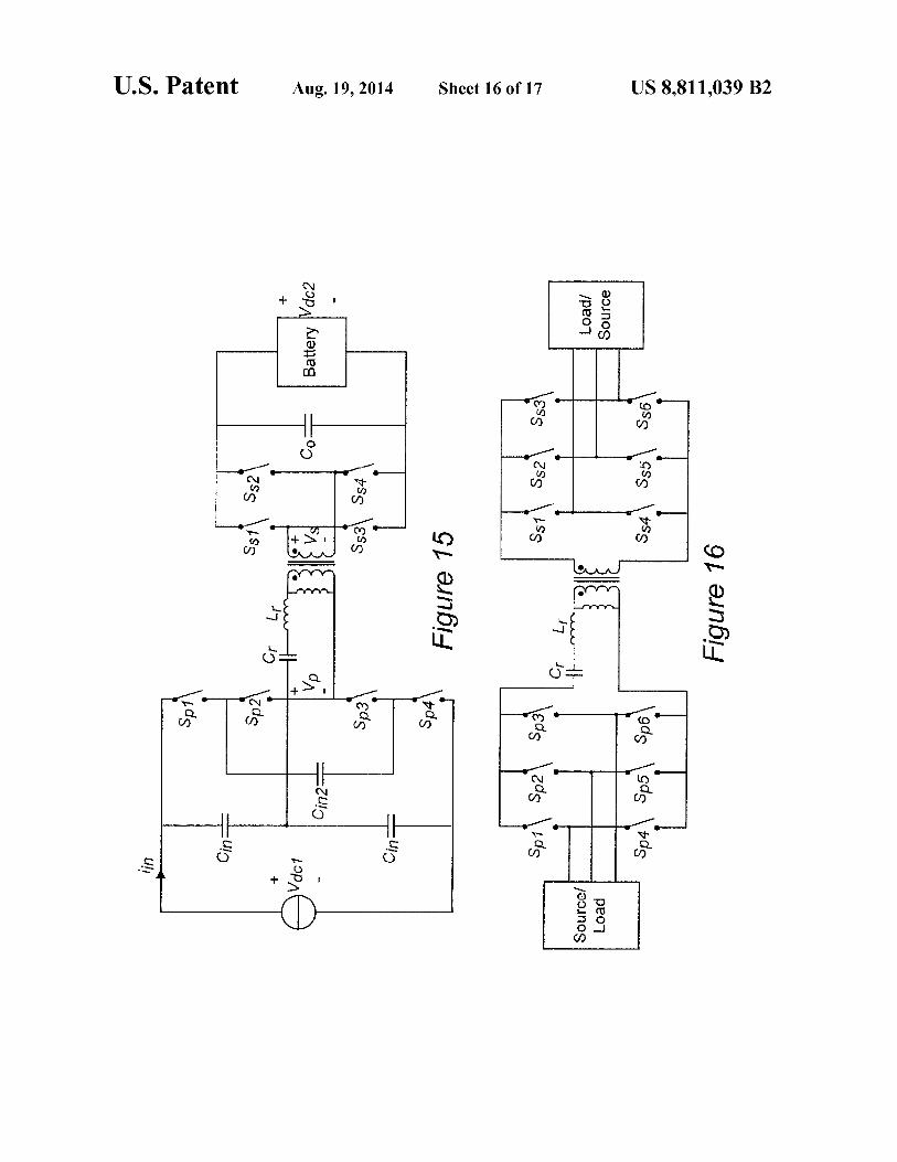
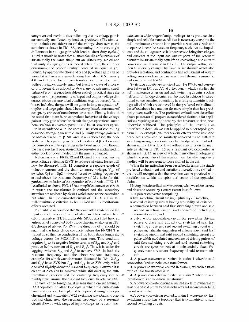
FIGS. 13, 14, 15 and 16 are schematic diagrams of further
embodiments illustrating application of the principle of the
invention to exemplary power converter variations and
topologies, and
FIG. 17 illustrates the basic methodology employed in
power conversion utilizing a null-immittance criterion.
DETAILED DESCRIPTION OF A PREFERRED
EMBODIMENT OF THE INVENTION
Referring now to the drawings, and more particularly to
FIG. 1, there is shown a high-level schematic diagram of the
architecture of a power system 100 as might be used for
powering a vehicle. In the system architecture illustrated,
while unimportant to the principles ofthe invention, power is
delivered from its ultimate source over, for example, distri-
bution system 110 as AC power. The delivered AC power is
then transformed into DC power using a rectifier arrangement
120 which is schematically illustrated as a full bridge rectifier
using four diodes but the details of the constitution and con-
figuration of the rectifier arrangement are unimportant to the
successful practice of the invention. A filter arrangement,
such as a filter capacitor, may be included as part of the
rectifier arrangement. The DC power so developed will then
be applied to a DC-DC converter 130 which can deliver
current at a suitable voltage to a battery 140 for storage.
Thereafter, the stored power can be applied to a motor 160 or
other load as DC power or, ifrequired by the load, AC power
developed by inverter 150.
10
25
35
40
45
50
4
It should also be appreciated that, for some applications, it
may be desirable to connect the inverter 150 in parallel with
the rectifier arrangement 120 to deliverAC power back to the
distribution system 110. It may also be desirable to provide
DC power to other DC loads, possibly at different voltages, in
addition to delivering power to motor 160. Therefore, it is
generally important and often required that DC-DC converter
130 be not only operable as a buck converter (e.g. to reduce
voltage) or a boost converter (e.g. to increase voltage) and
provide for bi-directional power flow as alluded to above. It is
also desirable for the DC-DC converter to be a switching
converter operable at a fixed frequency and to be easily con-
trollable using a fixed amplitude signal but having another
parameter that is continuously variable (or incrementally
variable with relatively fine increments) that can be devel-
oped by simple circuitry such as control by, for example,
pulse width modulation (PWM).
An example of a known DC-DC converter capable of at
least these functions is illustrated schematically in FIG. 2.
The circuit principally comprises a transformer connected
between two full-bridge (sometimes called H-bridge) switch-
ing circuits capable of reversing the direction of current flow
in the transformer windings or reversing the polarity of volt-
age appearing across the transformer windings by closing
switches in two opposite legs of the full bridge (e.g. Sp1 and
Sp2' or Ss1 and Ss2') while the other switches (e.g. Sp2 and
Sp1' or Ss2 and Ssl') are opened and vice-versa and is thus
commonly referred to as a dual active bridge (DAB) topology.
The Inductors Lr and Lm illustrated may be parasitic induc-
tance ofthe transformer (e.g. leakage inductance and magne-
tizing inductance) or may be added inductances to adjust
waveforms such that so-called soft switching may be
achievedby performing the switching whenvoltage on and/or
current through the switches is near zero. It is immaterial to
operation of this circuit whether the inductances are on the
primary side or secondary side or distributed between the
primary and secondary sides of the transformer. Thus, the
circuit of FIG. 1 functions as if it were entirely symmetrical
and, as such, can provide desirable bi-directional power flow.
The transformer also serves to provide isolation between the
respective sides of the circuit which is highly desirable, as
also alluded to above.
In operation, as is known, the direction and magnitude of
power transfer through the circuit is given by the equation:
P:NVdcl Vdc2¢(1—¢/W)/2nstV (1)
(Where N is the turns ratio of the transformer and q) is the
phase difference in switch control timing between the pri-
mary and secondary sides of the circuit) for the general case
of simple phase-shift modulation of the switching on the
primary and secondary sides of the circuit. Switch control
waveforms for phase shift modulation are shown in FIGS. 3A
and 3B.
A detailed discussion of the operation of the operation of
circuits of DAB topology is provided in “PWM Control of
Dual Active Bridge: Comprehensive Analysis and Experi-
mental Verification” by Jain et al., IEEE Transactions on
Power Electronics, Vol. 26, No. 4,April 201 1, pp. 1215-1227,
which is hereby incorporated by reference in its entirety and
includes analysis of a more general switching control tech-
nique that includes a combination of phase shift modulation
and pulse width modulation (PWM). Pulse width modulation
can be achieved simply by phase shifting the switching con-
trol signals in one leg of either or both of the primary and
secondary sides ofthe circuit by a phase angle, (X, with respect
to the other. Exemplary switching control waveforms show-
ing an exemplary relationship of (X and q) is illustrated in FIG.

US 8,811,039 B2
5
3C. The direction and magnitude ofpower transferwhen both
phase shift modulation and PWM are employed is given by
P:(8/n2)cos(oz/2)sin(0t+(q)/2))(NVdC2 Iggy
znfsw Vdcll’r (2)
As can be readily understood (and detailed in the above-
incorporated Jain et al. publication), when both phase shift
modulation and PWM are used together, particularly on both
the primary and secondary sides of a DAB topology circuit,
the equations for expressing power transfer become
extremely complicated. However, in qualitative terms,
because of the leakage inductance (which may be set, for
example, by an air gap in a leg of the transformer core or
similar structure andwhich can be supplemented, ifdesired or
needed, with additional series inductance), the voltage of the
primary side of the circuit can be controlled by the phase
modulation of switches on the primary side of the trans-
former. The same type ofmodulation can be employed on the
secondary side of the transformer to control the secondary
side voltage and the power transferred is controlled by the
phase shift between voltages at the primary side and the
secondary side of the circuit. Thus, use of phase shift modu-
lation and PWMmay require a complicated control scheme to
achieve voltage control since voltage gain is affected by both
switching frequency and load and, perhaps more importantly,
the asymmetric phase shifting of switch control. Moreover,
soft switching can only be achieved over a very narrow load
range and cannot be achieved at light loads because the cir-
culating currents are not high enough to discharge the para-
sitic capacitors ofthe switches. Low circulating current leads
to a small ZVS range which means high switching losses but
low conduction loss and switching losses then predominate
and limit overall efficiency.
In an effort to reduce large circulating currents and increase
the load range over which soft switching can be achieved, a
circuit topology illustrated in FIG. 4 has been proposed and is
discussed in detail in “Analysis and Design of High-Fre-
quency Isolated Dual-Bridge Series Resonant Converter” by
Li et al., IEEE Transactions on Power electronics, Vol. 25, No.
4, April 2010, which is also hereby incorporated by reference
in its entirety. The topology of this circuit is identical to that
of FIG. 2 but for the inclusion of a capacitor, Cr, having a
value that is resonant with the inductance, Lr. As discussed
therein, only phase modulation (but not PWM) is employed
for controlling the switches in the bridge circuits on the pri-
mary and secondary sides of the circuit. Large circulating
currents are not caused since there is no PWM (e.g. (F0)
applied. Exemplary operational waveforms are shown in FIG.
5 in which the angle 0 is the phase difference between the
resonant tank current and the output voltage and determines
whether the secondary side switches can achieve ZVS. As
will be discussed more fully below, ZVS can be achieved for
the secondary side switches only if 0<0. However, while
soft-switching can be achieved over an extended range in the
topology of FIG. 4, the voltage gain remains affected by both
load and frequency, variable switching frequency and a com-
plicated control scheme are required since voltage gain is
affected by phase shifting as well as load and switching
frequency. As with the circuit topology ofFIG. 2, the relative
phase of switching on the primary and secondary sides of the
circuit controls both the direction and magnitude of power
transfer and the voltage gain is similarly affected by both load
and switching frequency.
The inventors have discovered, however, that numerous
simplifications of control and operation as well as increased
functionality and improved performance can be achieved by
operating a circuit similar to that ofFIG. 4 at substantially the
10
15
20
25
30
35
40
45
50
55
60
65
6
resonant frequency using PWM only as illustrated in FIG. 6.
Exemplary operational waveforms are illustrated in FIG. 7.
FIGS. 6A-6D illustrate an exemplary circuit and operational
waveforms thereof for generating the operational waveforms
ofFIG. 7. That is, the inventors have discovered that the phase
shift modulation between the primary and secondary sides of
the circuit which cause asymmetry of the switching control
signals and require complicated circuitry can be omitted
entirely since the phase shifts that can be achieved by PWM
onthe primary and secondary sides ofthe circuit are sufficient
to control the voltage gain andpower transfer direction and do
so in a much less complicated manner.
Moreover, the inventors have discovered that PWM which
is symmetrical and synchronized on both the primary and
secondary sides of the circuit allows voltage gain to be inde-
pendent of load. Further, the inventors have discovered that
adequate control ofvoltage gain using PWM can be achieved
at a constant frequency which, ifset close to (e. g. at or slightly
above) the resonant frequency, can unconditionally provide
soft switching to guarantee high efficiency under any load
condition. Additionally, using symmetrical and synchronized
PWM switch control signals, allows the circuit ofFIG. 6 to be
operated in either a buck or boost mode; allowing the output
voltage to be continuously varied over a very wide range
while retaining bi-directional power transfer capabilities.
Specifically, symmetrical and synchronized PWM is pref-
erably achieved in accordance with the invention by applying
a threshold to a triangular waveform using a circuit such as
that of FIGS. 6A and 6B which will be discussed is greater
detail below. As the threshold is increased or decreased, the
points in time when a triangular waveform pulse crosses the
threshold will approach or separate from each other sym-
metrically around the maximum or peak of the triangular
waveform pulse, defining the switching points for a three-
level waveform. The phase angle between the maximum of
the triangular wave and the trailing edge of the primary or
secondary side voltage waveform are shown as (X and [3,
respectively, as illustrated in FIG. 7.
The circuit shown in FIG. 6A is the simulation file (and
thus contains an output circuit and “test points” (Vbridgin and
Vbridgout) that may be regarded as artifacts of simulation
which are unnecessary for successful practice of the inven-
tion) that shows the power stage of the PWM converter. The
switches shown in FIG. 6A are illustrated as ideal switches
and the parasitic capacitors and resistors and body diodes of
the switches shown in FIG. 6 are shown for purposes of
simulation and different reference numerals are applied for
that reason. C10 ofFIG. 6A corresponds to the output capaci-
tor Co ofFIG. 6 and the load of FIG. 6 is represented in FIG.
6A by R1. The tank circuit 610 comprising R1 and CL ofFIG.
6 are represented by L2 and C7 within dashed line 610' in FIG.
6A.
Referring now to FIG. 6B, when the PWM waveforms are
generated from a triangular waveform Vtmn as discussed
above, two pairs of T-flip-flops, triggered by the rising and
falling edges as shown in the phase shift block portion ofFIG.
6B, separately follow the PWM waveforms to achieve the
gate driver signals for the switch bridges on the primary and
secondary sides of the converter circuit. In the gate driver
signal generator block of FIG. 6B, buffers, and an array of
AND and OR gates are used to generate the complementary
gate driver signals with dead time for each phase leg. Alter-
natively the buffers illustrated can also be replaced by RC
circuits to generate the desired dead time. The operational
waveforms of FIGS. 6A and 6B are shown in FIGS. 6C and
6D for the primary and secondary side switch bridges. The

US 8,811,039 B2
7
eight outputs ofthe gate driver signal generator block are then
applied to the respective switches ofthe primary and second-
ary bridge circuits of FIG. 6A
Referring again to FIG. 7, the resulting voltages on the
primary and secondary sides ofthe circuit will thus be square
waves, the Fourier transform of which can be expressed as:
(3)N 4Vdcl
VP“) 2 2 7mn:l
Mt) = i
n:l
7m
sin(7 )sin(0m)sin(m)
(4)4Vdc2 . 7m . .WSln(7)sm(fin)sm(m)
In general, it is considered preferable to choose values of
Cr and Lr to have a series resonant frequency to match a
desired switching frequency for the converter. For a switching
frequency at or slightly above the resonant frequency, the
impedance of the resonant tank circuit formed by Cr and Lr
can be considered to be zero. As a result, the voltage across the
LrCr tank circuit at the fundamental frequency is forced to
zero.
This condition is referred to by the inventors and hereinaf-
ter as a null-immittance criterion since, if switching is per-
formed at a resonant frequency of a resonant circuit such that
the fundamental frequency of voltage across the resonant
circuit is forced to zero, the resonant circuit will emulate a
short circuit and both the voltages and currents at the input
and output ports ofthe resonant circuit are forced to be equal,
thereby achieving direct voltage and current conversion. This
criterion can thus be exploited in regard to any resonant
circuit and any switching topology at the input and output
ports of the resonant circuit and therefore many variant
embodiments of the invention are possible and can function
for conversion of any combination ofAC and DC input and
output voltages and currents. Switching is only necessary to
achieve PWM (although setting of switching frequency is
also simultaneously achieved) so that voltage variation can be
achieved by regulation of the current in the inductor and
consequent voltage developed across it which serves to trans-
fer powerthrough the converter circuit. Ifa DC voltage output
is required, any type of rectifier circuit can be employed and
bridge-type switching circuits should be understood as
merely exemplary of types of circuits that can operate bi-
directionally to convert between DC andAC. Notably, as will
be discussed below in connection with FIG. 13, a particularly
simple embodiment ofthe invention capable ofoperating as a
variable voltage converter capable ofoperating in accordance
with the invention as discussed herein need not include either
a transformer or control of switching on the secondary side of
the converter circuit (e.g. diodes can be used).
Thus, from equations (3) and (4) and considering the fun-
damental frequency components of the voltages to be equal,
the following simple equation can be derived:
Vdc2/Vdc1:sin(a)/N sin([5) (5)
Thus equation (5) shows that the ratio ofprimary and second-
ary side voltages is equal to the inverse ofthe ratio ofthe ratio
ofthe duty cycles ofthe primary and secondary side switches
(e.g. 20. and 2B for N:1) and thus the output voltage is
independent of load while operation at a constant, resonant
frequency avoids dependency of output voltage on switching
frequency. Further, the circuit will operate in a buck mode
when 0t<[3 and will operate in a boost mode when 0t>[3;
shifting seamlessly from one mode to the other as their rela-
tive values change. The efficacy of the invention to provide
10
15
20
25
30
35
40
45
50
55
60
65
8
operation in either a buck or boost mode has been confirmed
by simulation and will now be discussed with reference to
FIGS. 8-12.
In general, it is desirable to keep the pulse width of either
20. or 28 as large as possible. Therefore, to increase voltage
from a minimum value to a maximum value, it is preferable to
start with the duty cycle of Vs:2[3 at 50% and to increase
Vp:2ot from a minimal value to 50% where converter voltage
gain will be one and thereafter to further increase voltage gain
by decreasing 28 to a minimal value while maintaining the
duty cycle ofVp:20t at 50%. However, it should be observed
and kept in mind during the following discussion of FIGS.
8-12 that a given converter voltage gain can be obtained using
a continuum of duty cycles for (X and [3. For example, as long
as (F8 the converter voltage gain will be one (or N or 1/N if
N¢1) regardless of the duty cycle ofVp and Vs.
As shown in FIG. 8, the primary side voltage waveform
(Vp) duty cycle is set to 50% (0t:180°/2:90°; the dead time
appearing at both the leading and trailing edges of the PWM
pulse) and [3 is used as the control variable. Exemplary values
for [3 of 15°, 45° and 75° are shown for the secondary side
voltage, Vs. The other simulation conditions were:
Vdcl:120 Volts
fs:1.0 MHZ
f0:0.998 MHZ (resonant frequency)
Power:13 kW (full load)
N:1.
The resulting inductor current iL and secondary side output
voltage, Vdcz, are shown in FIG. 9. Recalling that the differ-
ence in voltages at the primary and secondary side windings
ofthe transformer appears as a voltage across the inductor as
a function of the current therethrough and the switching is
performed at substantially the resonant frequency ofthe con-
verter, the inductor current is substantially a sinusoidal wave-
formhaving a peak voltage that substantially follows (but lags
behind in phase) the peak secondary winding voltage. The
filtered output voltage, Vdcz, is substantially proportional to
the peak inductor current. Thus, it is seen that the synchro-
nized symmetrical switching ofthe converter circuit in accor-
dance with the invention is clearly capable of operating in a
boost mode with the output voltage increasing with decreas-
ing [3. It should be noted that buck mode operation is not
exhibited in FIGS. 8 and 9 since [3<0t for the simulations
illustrated. These results are fully consistent with the
expected function of the invention as described above.
Referring now to FIG. 10, the converse simulation switch-
ing waveforms are depicted. That is, [3 is set to 90° and a is
varied as the control variable. In this case, the simulated
response is entirely consistent with equation (5) above and the
proportionality of the output voltage to the input voltage is
equal to sin(0t)/sin([3). Since [3:90°, sin([3):1 and thus V0162
equals V016l sin(0t); corresponding to buck mode operation.
The simulation results discussed above are summarized in
FIG. 11 from which several other observations can be made
confirming the predicted performance of the invention. Spe-
cifically FIG. 11 illustrates three families of curves showing
voltage gain as a function of [3 for three different values of (X,
respectively. The respective curves of each family of curves
indicate voltage gain (e.g. the ratio of output voltage to input
voltage) for different loads and include the calculated, theo-
retical voltage gain as discussed above.
First of all, it should be noted that all curves are in good
agreement with the calculated voltage gain, thus indicating
that the invention is capable ofproducing the predicted results
that the inventors have theorized and evidently confirming the
theory of operation of the invention as discussed above. Sec-
ond, the curves of each family of curves are substantially
US 8,811,039 B2
9
congruent and overlaid, thus indicating that the voltage gain is
substantially unaffected by load, as predicted. (The simula-
tion includes consideration of the voltage drop across the
switches as shown in FIG. 6A, accounting for the very slight
differences in voltage gain with load at short duty cycles.)
Third, it shouldbe noted that all three families ofcurves are of
substantially the same shape but are differently scaled and
that unity voltage gain is achieved when [3:0t, thus further
confirming the proportionality indicated in equation (5).
Fourth, by appropriate choice of (X and [3, voltage gain can be
varied at will over a range extending from about 0.5 to nearly
4.0, an 0:1 ratio for a given transformer turns ratio, even
without using extremely small but feasible values of either (X
or [3. In general, as alluded to above, use of extremely small
values of(X or [3 are not desirable or entirely practical since the
equations of proportionality of input and output voltage dis-
cussed above assume ideal conditions (e.g. no losses). With
losses included, the gain will not go to infinity as equation (5)
implies and large gains shouldbe accomplished, as a matter of
design, by choice oftransformer turns ratio. Finally, it should
be noted that there is no anomalous behavior of the voltage
gain at unity gain where the circuit changes operational mode
between buck converter operation and boost converter opera-
tion in accordance with the above discussion of controlling
converter voltage gain with (X and [3. Unity voltage gain will
be obtained when (x:[3:90° and, if (X is decreased, the con-
verter will be operating in the buck mode or, if [3 is decreased
the converter will be operating in the boost mode even though
the basic electrical operation ofthe converter is unchanged in
either buck or boost mode; only the gain is changed.
Referring now to FIGS. 12 and 13, conditions for achieving
zero voltage switching (ZVS) to reduce switching losses will
now be discussed. FIG. 12 comprises a separate graph of
inductor current and the drain-to-source voltage, Vd5, of
switches Sp1 and Sp2 for two different switching frequencies
at and above the resonant frequency of 219 KHZ for this
particular simulation ofthe operation ofthe circuit ofFIG. 13.
As alluded to above, FIG. 13 is a simplified converter circuit
in which the transformer is omitted and the secondary
switches are replaced by diodes which need not be controlled
but which, like the converter circuit of FIG. 6, allows the
null-immittance criterion to be utilized and its meritorious
effects obtained.
It should be understood that the controlled switches on the
input side of the circuit are not ideal switches but are field
effect transistors (FETs, preferably MOSFETs) that have an
anti-parallel connected body diode therein, as shown in FIG.
6A discussed above. For ZVS, the direction of iL should be
such that the body diode conducts before the MOSFET is
turned on so that the conduction of the body diode brings the
voltage across the MOSFET to near zero. This condition
requires iL to be negative before turn on of SP1 and SP 1' and
positive before turn on of Sp2 and Spl'. Thus, it is easier for
lagging switches Sp2 and SP2' to achieve ZVS. In both the
resonant frequency and the above-resonant frequency
examples for which waveforms are illustrated in FIG. 12, Sp2
and sz' have ZVS but SP1 and SP1' have ZVS only when
operated slightly above the resonant frequency. However, it is
clear that ZVS can be achieved while still meeting the null-
immittance criterion and the switching frequency can be
readily tuned around the resonant frequency to achieve ZVS.
In view of the foregoing, it is seen that a circuit having a
DAB topology or other topology in which the null-immit-
tance criterion can be exploited but operated using only syn-
chronized and symmetric PWM switching waveforms to con-
trol switching near the resonant frequency of a resonant
circuit allows a wide range of input voltages to be accommo-
10
15
20
25
30
35
40
45
50
55
60
65
10
dated and a wide range of output voltages to be produced in a
simple and reliable manner. All that is necessary to exploit the
null-immittance criterion is to provide a resonant circuit and
to operate it near the resonant frequency such that the imped-
ance and the voltage across it is near zero to bring the voltages
and currents at the input and output ports of the resonant
circuit to be substantially equal for direct voltage and current
conversion as illustrated in FIG. 17. The output voltage can
then be coarsely changed by use of a transformer which also
provides isolation, and continuous fine adjustment of output
voltage over a wide range can be achieved through symmetric
and synchronized PWM.
Switching circuits are required only for PWM and conver-
sion between DC and AC at a frequency which satisfies the
null-immittance criterion and such switching circuits, such as
half and full bridge circuits, can be used to achieve bi-direc-
tional power transfer, potentially in a fully symmetric topol-
ogy; all of which are achieved in the preferred embodiment
described above in a manner far more simple than has previ-
ously been available. The preferred embodiment described
above possesses all properties considered desirable for appli-
cations requiring storage ofenergy that have not, to date, been
otherwise achieved. The principles of the invention as
described in detail above can be applied to other topologies,
as well. For example, the meritorious effects of the invention
described above can be similarly achieved using different
switching arrangements such as a halfbridge at the input side,
shown in FIG. 14, a three level voltage converter on the input
side as shown in FIG. 15 or a resonant cycloconverter as
shown in FIG. 16; in view ofwhich, many other topologies to
which the principles of the invention can be advantageously
applied will be apparent to those skilled in the art.
While the invention has been described in terms ofa single
preferred embodiment and variations thereof, those skilled in
the art will recognize that the invention can be practiced with
modification within the spirit and scope of the appended
claims.
Having thus described our invention, what we claim as new
and desire to secure by Letters Patent is as follows:
1. A power converter comprising
a first switching circuit having a plurality of switches,
a second switching circuit having a plurality of switches,
a connection between said first switching circuit and said
second switching circuit, said connection including a
resonant circuit, and
a pulse width modulation circuit for providing driving
pulses to drive said plurality of switches of said first
switching circuit and said second switching circuit with
pulses such that driving pulses ofat least one of said first
switching circuit and said second switching circuit are
pulse width modulated and centers of driving pulses of
said first switching circuit and said second switching
circuit are synchronized at a substantially fixed fre-
quency near a resonant frequency of said resonant cir-
cuit.
2. A power converter as recited in claim 1 wherein said
connection further includes a transformer.
3. A power converter as recited in claim 2, wherein a turns
ratio of said transformer is 1:1.
4. A power converter as recited in claim 2 wherein said
transformer is an isolation transformer.
5. A power converter circuit as recited in claim 2 wherein at
least one ofsaid plurality ofswitches ofsaid second switching
circuit is a diode.
6. A power converter as recited in claim 2, wherein said first
switching circuit has a topology that is symmetrical to said
second switching circuit.

US 8,811,039 B2
11
7. A power converter as recited in claim 2, wherein said
resonant circuit comprises a series connected inductor and
capacitor.
8. A power converter as recited in claim 7 wherein said
inductor comprises a leakage inductance of a transformer.
9. A power converter as recited in claim 2, wherein said first
switching circuit is a full bridge circuit.
10. A power converter as recited in claim 1 wherein at least
one of said plurality of switches of said second switching
circuit is a diode.
11. A power converter as recited in claim 1, wherein said
first switching circuit has a topology that is symmetrical to
said second switching circuit.
12. A power converter as recited in claim 1, wherein said
resonant circuit comprises a series connected inductor and
capacitor.
13. A power converter as recited in claim 12 wherein said
inductor comprises a leakage inductance of a transformer.
14. A power converter as recited in claim 1, wherein said
first switching circuit is a full bridge circuit.
15
12
15. The power converter as recited in claim 1, wherein said
resonant circuit is a series resonant circuit.
1 6. A method ofoperating a power converter circuit having
first and second switching circuits, each switching circuit
comprising a plurality of switches connected to provide con-
version between AC and DC voltage, and a resonant circuit,
said resonant circuit connecting said first and second switch-
ing circuits, said method comprising
controlling switches ofat least said first switching circuit to
provide pulse width modulated current in said resonant
circuit at a substantially fixed frequency near a resonant
frequency of said resonant circuit such that centers ofthe
duty cycles ofrespective switches of said second switch-
ing circuit are substantially synchronized and substan-
tially symmetrical about centers of said duty cycles of
respective switches of said first switching circuit.
17. The method as recited in claim 16, wherein said reso-
nant circuit is a series resonant circuit.
* * * * *
![ñZ ]vP ]À ^o Dïïñ : ¬óñìUììì...ñZ ]vP ]À ^o Dïïñ : ¬óñìUììì &h>>zZ &hZ /^, dK^/DW>zD /E'^dE Z E Dh^d s/ t JJ,KD ^dd ' Ed^ ]À]o P } ]vP } Z u l Z] (}µ](https://img.pdfslide.us/doc/110x75/5e3a60bab05e8f7bfb6cedf8/z-vp-o-d-u-z-vp-o-d-u.jpg)

![D]v]vP Z tKD }( Z ZW^ µPPo }(/v ]P v}µ t}u vP]v µ À u]v]vP · Lepanto Consolidated Mining Company/Gold Fields LimitedCo. (Jacqueline Sakiwat Buli-e) 4. Indonesia, Nusa Tenggara](https://img.pdfslide.us/doc/110x75/5e4f1ee886040d1db27029e1/dvvp-z-tkd-z-zw-ppo-v-p-v-tu-vpv-uvvp-lepanto-consolidated.jpg)
![$01 · E%$>#-%$(,%.!E*;#.(+&!*5!@*-).#/!D04$#-4 !! ! ! !!!!!D Z u oD} o]vP}( }u o Æ^Ç u !!D$*!,%+!%)).0?!!vÇ(µ Z µ }v MWo }v µ J](https://img.pdfslide.us/doc/110x75/5d66bc4f88c99364418b4778/01-e-e5-d04-4-d-z-u-od-ovp-u.jpg)


![2017 WORKSHOP SERIES...v D]v vv August 2 îìíó o Z]v o v v PÇ > Sept 1 /v } µ }v } µ]o ]vP v PÇD} o]vP Sept 222 D] }ZÇ }^Ç u ]Pv /v oo }v Sept 2 o} ]vP Z >}} WtZÇ }t E W}](https://img.pdfslide.us/doc/110x75/600a7b5019d6b843fa21d5b1/2017-workshop-series-v-dv-vv-august-2-o-zv-o-v-v-p-sept-1.jpg)


![by subm~Ued, DONALD E. PEHLKE AND CHARLES D. WELLER · CHARLES P. SMITH, DONALD E. PEHLKE AND CHARLES D. WELLER PROJECT STAR DECEMBER, 1974 /(Ç}µZÀ ] µ À] Á]vP} ]vP Z] (]o }v](https://img.pdfslide.us/doc/110x75/5e1912606c47af6feb5410fa/by-submued-donald-e-pehlke-and-charles-d-weller-charles-p-smith-donald-e.jpg)


![PowerPoint Presentation · ^ D/E Á} l]vP Ç^W lP]vP - < Ç(} ^Ç u/v P ]}v_ JUN/27, 2013 @ NANIUM, Vila do Conde, Portugal Highlights: x Around 100 participants e xpected x Event](https://img.pdfslide.us/doc/110x75/5bec204b09d3f2cb5e8c5b91/powerpoint-de-a-lvp-cw-lpvp-c-c-uv-p-v-jun27-2013-.jpg)


![^ o]À ]vP }u} }Á[ ^}oµ ]}v d} Ç - SINGELA](https://img.pdfslide.us/doc/110x75/6169cd4211a7b741a34b84f6/-o-vp-u-o-v-d-singela.jpg)


![Vp%5 B1%5 D[1]](https://img.pdfslide.us/doc/110x75/557a35efd8b42a32248b4925/vp5-b15-d1.jpg)