Embed Size (px)
Citation preview
INSTITUTE OF PHYSICS PUBLISHING JOURNAL OF MICROMECHANICS AND MICROENGINEERING
J. Micromech. Microeng. 12 (2002) 87–95 PII: S0960-1317(02)28226-1
Fabrication of thick silicon dioxidesacrificial and isolation blocks in asilicon substrateHongrui Jiang1,5, Kyutae Yoo1, Jer-Liang Andrew Yeh2,6,Zhihong Li1,4,7 and Norman C Tien3
1 School of Electrical and Computer Engineering, Cornell University, Ithaca, NY 14853, USA2 Advanced Integrated Photonics, Inc, Fremont, CA 94538, USA3 Department of Electrical and Computer Engineering, University of California at Davis,Davis, CA 95616, USA4 Institute of Microelectronics, Peking University, Beijing 100871, People’s Republic ofChina
Received 22 August 2001, in final form 24 October 2001Published 11 December 2001Online at stacks.iop.org/JMM/12/87
AbstractA silicon micromachining method that is able to create deep silicon dioxideblocks at selected locations in a silicon substrate is presented. The processcombines deep-reactive-ion etching (DRIE), thermal oxidation, depositionof silicon dioxide and optional planarization. Design issues and parametersfor the creation of such blocks are discussed. The selectively defined silicondioxide blocks allow the integration of silicon surface and bulkmicromachining and thick large-area isolation regions for integratedcircuits. The performance enhancement that this approach enables isexemplified in the fabrication of an on-chip tunable capacitor and amonolithic transformer on 20-µm-deep silicon dioxide blocks.
1. Introduction
On-chip passive components have attracted a lot of interestin recent years because they are very important in radio-frequency (RF) circuits, which have widespread applicationsin wireless communication systems [1, 2]. The performanceof current components, such as inductors, transformers andtunable capacitors, however, could be much improved. On-chip inductors and transformers generally suffer from lowquality factors (Q) and low self-resonant frequencies (fres)[1, 3–6]. One of the main reasons is the lack of a thick isolationlayer between the device and the silicon substrate below. Theeddy current induced in the substrate by the electromagneticfield generated by the inductor and the transformer introducesloss of energy and lowers Q [3, 5, 6]. Furthermore, the parasiticcapacitance between the device and the substrates sets a limit
5 Present address: Berkeley Sensor and Actuator Center, University ofCalifornia Berkeley, Berkeley, CA 94720, USA.6 Present address: Department of Power Mechanical Engineering, NationalTsing-Hua University, Shinchu, Taiwan.7 Present address: Department of Electrical and Computer Engineering,University of California at Davis, Davis, CA 95616, USA.
to fres of the device, thus its functional frequency range [4–6].Current on-chip tunable capacitors, generally realized by elec-trostatically actuated parallel plates, have a similar problem.Because of the closeness between the bottom plate of the ca-pacitor and the silicon substrate, the parasitic capacitance ison the same order of magnitude as the functional capacitancebetween the plates. Therefore, the tuning ratio of such capac-itors is severely impaired [7]. A direct remedy to these issuesis to deposit a thick layer of insulating material such as silicondioxide [7]; the electromagnetic coupling and the parasiticsbetween the devices and the substrate can be greatly reduced,thus enhancing the device performance. However, depositionof a very thick, say more than 10 µm, insulating film acrossthe wafer, is hard to realize and will introduce other difficultiesin processing such as making contacts with the substrate. Thestress distribution in a thick deposited film can also induce alarge bending moment on the substrate that would severelybend the wafer. The residual stress and built-in stress gradientof a thick deposited film may cause the film to crack as well.Other techniques have been developed to form ‘localized’ in-sulating layers in the substrate underneath specific devices,such as etching holes into the silicon substrate under partic-ular devices and filling them with borophosphosilicate glass
0960-1317/02/010087+09$30.00 © 2002 IOP Publishing Ltd Printed in the UK 87
H Jiang et al
Polysilicon
Single-crystal silicon
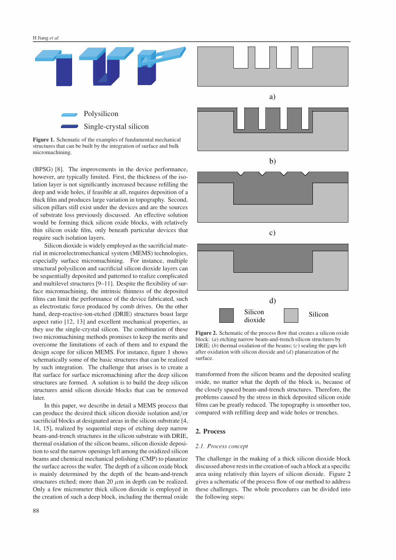
Figure 1. Schematic of the examples of fundamental mechanicalstructures that can be built by the integration of surface and bulkmicromachining.
(BPSG) [8]. The improvements in the device performance,however, are typically limited. First, the thickness of the iso-lation layer is not significantly increased because refilling thedeep and wide holes, if feasible at all, requires deposition of athick film and produces large variation in topography. Second,silicon pillars still exist under the devices and are the sourcesof substrate loss previously discussed. An effective solutionwould be forming thick silicon oxide blocks, with relativelythin silicon oxide film, only beneath particular devices thatrequire such isolation layers.
Silicon dioxide is widely employed as the sacrificial mate-rial in microelectromechanical system (MEMS) technologies,especially surface micromachining. For instance, multiplestructural polysilicon and sacrificial silicon dioxide layers canbe sequentially deposited and patterned to realize complicatedand multilevel structures [9–11]. Despite the flexibility of sur-face micromachining, the intrinsic thinness of the depositedfilms can limit the performance of the device fabricated, suchas electrostatic force produced by comb drives. On the otherhand, deep-reactive-ion-etched (DRIE) structures boast largeaspect ratio [12, 13] and excellent mechanical properties, asthey use the single-crystal silicon. The combination of thesetwo micromachining methods promises to keep the merits andovercome the limitations of each of them and to expand thedesign scope for silicon MEMS. For instance, figure 1 showsschematically some of the basic structures that can be realizedby such integration. The challenge that arises is to create aflat surface for surface micromachining after the deep siliconstructures are formed. A solution is to build the deep siliconstructures amid silicon dioxide blocks that can be removedlater.
In this paper, we describe in detail a MEMS process thatcan produce the desired thick silicon dioxide isolation and/orsacrificial blocks at designated areas in the silicon substrate [4,14, 15], realized by sequential steps of etching deep narrowbeam-and-trench structures in the silicon substrate with DRIE,thermal oxidation of the silicon beams, silicon dioxide deposi-tion to seal the narrow openings left among the oxidized siliconbeams and chemical mechanical polishing (CMP) to planarizethe surface across the wafer. The depth of a silicon oxide blockis mainly determined by the depth of the beam-and-trenchstructures etched; more than 20 µm in depth can be realized.Only a few micrometer thick silicon dioxide is employed inthe creation of such a deep block, including the thermal oxide
a)
b)
c)
d)
SiliconSilicondioxide
Figure 2. Schematic of the process flow that creates a silicon oxideblock: (a) etching narrow beam-and-trench silicon structures byDRIE; (b) thermal oxidation of the beams; (c) sealing the gaps leftafter oxidation with silicon dioxide and (d) planarization of thesurface.
transformed from the silicon beams and the deposited sealingoxide, no matter what the depth of the block is, because ofthe closely spaced beam-and-trench structures. Therefore, theproblems caused by the stress in thick deposited silicon oxidefilms can be greatly reduced. The topography is smoother too,compared with refilling deep and wide holes or trenches.
2. Process
2.1. Process concept
The challenge in the making of a thick silicon dioxide blockdiscussed above rests in the creation of such a block at a specificarea using relatively thin layers of silicon dioxide. Figure 2gives a schematic of the process flow of our method to addressthese challenges. The whole procedures can be divided intothe following steps:
88
Fabrication of thick silicon dioxide sacrificial and isolation blocks
2 µm1 µm
60 µm
Silicon beamsTrenches
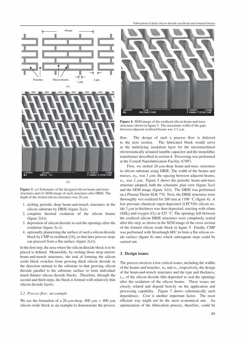
(a)
(b)
Figure 3. (a) Schematic of the designed silicon beam-and-trussstructures and (b) SEM image of such structures after DRIE. Thedepth of the etched silicon structures was 20 µm.
1. etching periodic deep beam-and-trench structures in thesilicon substrate by DRIE (figure 2(a));
2. complete thermal oxidation of the silicon beams(figure 2(b));
3. deposition of silicon dioxide to seal the openings after theoxidation (figure 2(c));
4. optionally planarizing the surface of such a silicon dioxideblock by CMP or etchback [16], so that later process stepscan proceed from a flat surface (figure 2(d)).
In the first step, the area where the silicon dioxide block is to beplaced is defined. Meanwhile, by etching those deep narrowbeam-and-trench structures, the task of forming the siliconoxide block switches from growing thick silicon dioxide inthe direction normal to the substrate to that growing silicondioxide parallel to the substrate surface to form individualmuch thinner silicon dioxide blocks. Therefore, through thesecond and third steps, the block is formed with relatively thinsilicon dioxide layers.
2.2. Process flow: an example
We use the formation of a 20-µm-deep, 400 µm × 400 µmsilicon oxide block as an example to demonstrate the process
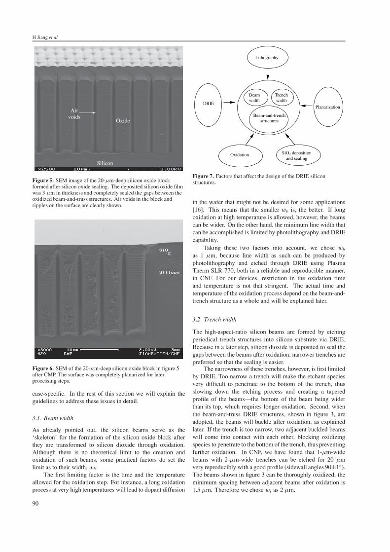
Figure 4. SEM image of the oxidized silicon beam-and-trussstructures shown in figure 3. The maximum width of the gapsbetween adjacent oxidized beams was 2.5 µm.
flow. The design of such a process flow is deferredto the next section. The fabricated block would serveas the underlying insulation layer for the micromachinedelectrostatically actuated tunable capacitor and the monolithictransformer described in section 4. Processing was performedat the Cornell Nanofabrication Facility (CNF).
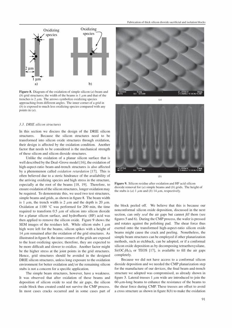
First, we etched 20-µm-deep beam-and-truss structuresin silicon substrate using DRIE. The width of the beams andtrusses, wb, was 1 µm; the spacing between adjacent beams,wt , was 2 µm. Figure 3 shows the periodic beam-and-trussstructure adopted, both the schematic plan view (figure 3(a))and the SEM image (figure 3(b)). The DRIE was performedon a Plasma Therm SLR-770. Next, the DRIE structures werethoroughly wet oxidized for 260 min at 1100 ◦C (figure 4). Alow-pressure chemical-vapor-deposited (LPCVD) silicon ox-ide 3 µm in thickness was then deposited, reacting with silane(SiH4) and oxygen (O2) at 425 ◦C. The openings left betweenthe oxidized silicon DRIE structures were completely sealedafter this step, as shown in the SEM image of the cross sectionof the formed silicon oxide block in figure 5. Finally, CMPwas performed with Strasbaugh 6EC to form a flat silicon ox-ide surface (figure 6) onto which subsequent steps could becarried out.
3. Design issues
The process involves a few critical issues, including the widthsof the beams and trenches, wb and wt , respectively, the designof the beam-and-trench structures and the type and thickness,tox, of the silicon dioxide film deposited to seal the openingsafter the oxidation of the silicon beams. These issues areclosely related and depend heavily on the application andprocessing capability. Figure 7 shows schematically suchdependence. Cost is another important factor. The mostefficient way might not be the most economical one. Anoptimization of the fabrication process, therefore, could be
89
H Jiang et al
Oxide
Silicon
Airvoids
Figure 5. SEM image of the 20-µm-deep silicon oxide blockformed after silicon oxide sealing. The deposited silicon oxide filmwas 3 µm in thickness and completely sealed the gaps between theoxidized beam-and-truss structures. Air voids in the block andripples on the surface are clearly shown.
Figure 6. SEM of the 20-µm-deep silicon oxide block in figure 5after CMP. The surface was completely planarized for laterprocessing steps.
case-specific. In the rest of this section we will explain theguidelines to address these issues in detail.
3.1. Beam width
As already pointed out, the silicon beams serve as the‘skeleton’ for the formation of the silicon oxide block afterthey are transformed to silicon dioxide through oxidation.Although there is no theoretical limit to the creation andoxidation of such beams, some practical factors do set thelimit as to their width, wb.
The first limiting factor is the time and the temperatureallowed for the oxidation step. For instance, a long oxidationprocess at very high temperatures will lead to dopant diffusion
Lithography
Beam-and-trenchstructures
Beamwidth
Trenchwidth
DRIE
Oxidation SiO2 depositionand sealing
Planarization
Figure 7. Factors that affect the design of the DRIE siliconstructures.
in the wafer that might not be desired for some applications[16]. This means that the smaller wb is, the better. If longoxidation at high temperature is allowed, however, the beamscan be wider. On the other hand, the minimum line width thatcan be accomplished is limited by photolithography and DRIEcapability.
Taking these two factors into account, we chose wb
as 1 µm, because line width as such can be produced byphotolithography and etched through DRIE using PlasmaTherm SLR-770, both in a reliable and reproducible manner,in CNF. For our devices, restriction in the oxidation timeand temperature is not that stringent. The actual time andtemperature of the oxidation process depend on the beam-and-trench structure as a whole and will be explained later.
3.2. Trench width
The high-aspect-ratio silicon beams are formed by etchingperiodical trench structures into silicon substrate via DRIE.Because in a later step, silicon dioxide is deposited to seal thegaps between the beams after oxidation, narrower trenches arepreferred so that the sealing is easier.
The narrowness of these trenches, however, is first limitedby DRIE. Too narrow a trench will make the etchant speciesvery difficult to penetrate to the bottom of the trench, thusslowing down the etching process and creating a taperedprofile of the beams—the bottom of the beam being widerthan its top, which requires longer oxidation. Second, whenthe beam-and-truss DRIE structures, shown in figure 3, areadopted, the beams will buckle after oxidation, as explainedlater. If the trench is too narrow, two adjacent buckled beamswill come into contact with each other, blocking oxidizingspecies to penetrate to the bottom of the trench, thus preventingfurther oxidation. In CNF, we have found that 1-µm-widebeams with 2-µm-wide trenches can be etched for 20 µmvery reproducibly with a good profile (sidewall angles 90±1◦).The beams shown in figure 3 can be thoroughly oxidized; theminimum spacing between adjacent beams after oxidation is1.5 µm. Therefore we chose wt as 2 µm.
90
Fabrication of thick silicon dioxide sacrificial and isolation blocks
2 µm
1 µma) b)
Oxidizingspecies
Oxidizingspecies
Figure 8. Diagram of the oxidation of simple silicon (a) beam and(b) grid structures; the width of the beams is 1 µm and that of thetrenches is 2 µm. The arrows symbolize oxidizing speciesapproaching from different angles. The inner corner of a grid in(b) is exposed to much less oxidizing species compared with anypoints in (a).
3.3. DRIE silicon structures
In this section we discuss the design of the DRIE siliconstructures. Because the silicon structures need to betransformed into silicon oxide structures through oxidation,their design is affected by the oxidation condition. Anotherfactor that needs to be considered is the mechanical strengthof these silicon and silicon dioxide structures.
Unlike the oxidation of a planar silicon surface that iswell described by the Deal–Grove model [16], the oxidation ofhigh-aspect-ratio beam-and-trench structures is also affectedby a phenomenon called oxidation retardation [17]. This isoften believed due to a steric hindrance of the availability ofthe arriving oxidizing species and high stress in the structure,especially at the root of the beams [18, 19]. Therefore, toensure oxidation of the silicon structures, longer oxidation maybe required. To demonstrate this, we used two test structures,simple beams and grids, as shown in figure 8. The beam widthis 1 µm, the trench width is 2 µm and the depth is 20 µm.Oxidation at 1100 ◦C was performed for 200 min, the timerequired to transform 0.5 µm of silicon into silicon dioxidefor a planar silicon surface, and hydrofluoric (HF) acid wasthen applied to remove the silicon oxide. Figure 9 shows theSEM images of the residues left. While silicon stubs 1 µmhigh were left for the beams, silicon spikes with a height of14 µm remained after the oxidation of the grid structures. Asillustrated in figure 8, the inner corners of the grids are exposedto the least oxidizing species; therefore, they are expected tobe more difficult and slower to oxidize. Another factor mightbe the higher stress at the joint points in the grid structures.Hence, grid structures should be avoided in the designedDRIE silicon structures, unless long exposure to the oxidationenvironment for better oxidation and/or the remaining siliconstubs is not a concern for a specific application.
The simple beam structures, however, have a weakness.It was observed that after oxidation of these beams anddeposition of silicon oxide to seal the air gaps, the siliconoxide block thus created could not survive the CMP process.In most cases cracks occurred and in some cases part of
(a)
(b)
Figure 9. Silicon residue after oxidation and HF acid silicondioxide removal for (a) simple beams and (b) grids. The height ofthe stubs is (a) 1 µm and (b) 14 µm, respectively.
the block peeled off. We believe that this is because ournonconformal silicon oxide deposition, discussed in the nextsection, can only seal the air gaps but cannot fill them (seefigures 5 and 6). During the CMP process, the wafer is pressedand rotates against the polishing pad. The shear force thusexerted onto the transformed high-aspect-ratio silicon oxidebeams might cause the crack and peeling. Nonetheless, thesimple beam structures can be employed if other planarizationmethods, such as etchback, can be adopted, or if a conformalsilicon oxide deposition as by decomposing tetraethoxysilane,Si(OC2H5)4 or TEOS [17], is available to fill the air gapscompletely.
Because we did not have access to a conformal silicondioxide deposition and we needed the CMP planarization stepfor the manufacture of our devices, the final beam-and-trenchstructure we adopted was compromised, as already shown infigure 3. Lateral trusses 1 µm wide are introduced to join the60-µm-long beams to enhance the resistance of the beams tothe shear force during CMP. These trusses are offset to avoida cross structure as shown in figure 8(b) to make the oxidation
91
H Jiang et al
a) b)
φ1 φ2TT=0
2T3T
T=0
2T3T
T
Time Time
φ1=45° φ2>45°Sealed
Sealed
Airvoid
Filled
Figure 10. Schematic of the sealing of a trench by silicon oxideusing (a) conformal and (b) nonconformal deposition as timeevolves. The trench is completely filled with conformal deposition.The corners of the trench are moving upward at an angle of 45◦
because the deposition rates at the top surface and on the sidewallsare the same. With nonconformal deposition, the deposition rate atthe top surface is larger than that on the sidewalls and the corners ofthe trench are moving upward at an angle larger than 45◦. Thickerfilm is required to seal the trench than that required to fill the trenchwith conformal deposition; the sealing point is also higher. Thetrench cannot be filled but can only be sealed and an air void will beleft after the sealing.
retardation less severe. After oxidation, the volume of thebeams expands by a factor of 2.27 [17]. The long beamsand the trusses experience expansion in different directions,causing the beams to buckle and widening some of the airgaps. The widened air gaps make their sealing more difficultduring the silicon oxide deposition, as discussed in the nextsection. Therefore, less buckling is preferred. The degreeof buckling varies with the length of the beams. Generallyspeaking, the longer the beams are, the more the buckling,thus wider air gaps. On the other hand, structures with shorterbeams with the trusses require a longer time for the patterngenerator to make the mask for photolithography. The choiceof 60-µm-long beams was what we found the best compromisebetween the maximum width of the air gaps and the amount oftime required for pattern generation. In practice, the structuresof beams and trusses underwent a wet oxidation of 260 minat 1100 ◦C, 1 h more than required to oxidize 0.5-µm-thicksilicon for a planar silicon surface to better oxidize the jointsof the beams and trusses. The observed maximum width ofthe air gaps after oxidation was 2.5 µm, much smaller than theupper limit of 4 µm we found, as will be explained next.
3.4. SiO2 deposition
The purpose of silicon oxide deposition is to seal the air gapsleft after the oxidation of the beams, thus, as mentioned above,creating much smaller individual blocks with relatively thinsilicon oxide layer. Generally speaking, the lesser the need toseal the trenches is, the better. Therefore, better step coverageis more desirable.
Figure 10 schematically diagrams the trench sealing pro-cess with conformal and nonconformal deposited films. Inthe case of a conformal deposition, the deposition rate on thetop surfaces is equal to that on the sidewalls of the trenches.Therefore, the corners of the trench moving upward at an angleof 45◦. The trench is then sealed and completely filled aftera deposition of half the width of the trench, regardless of itsdepth (figure 10(a)). On the other hand, when the deposition is
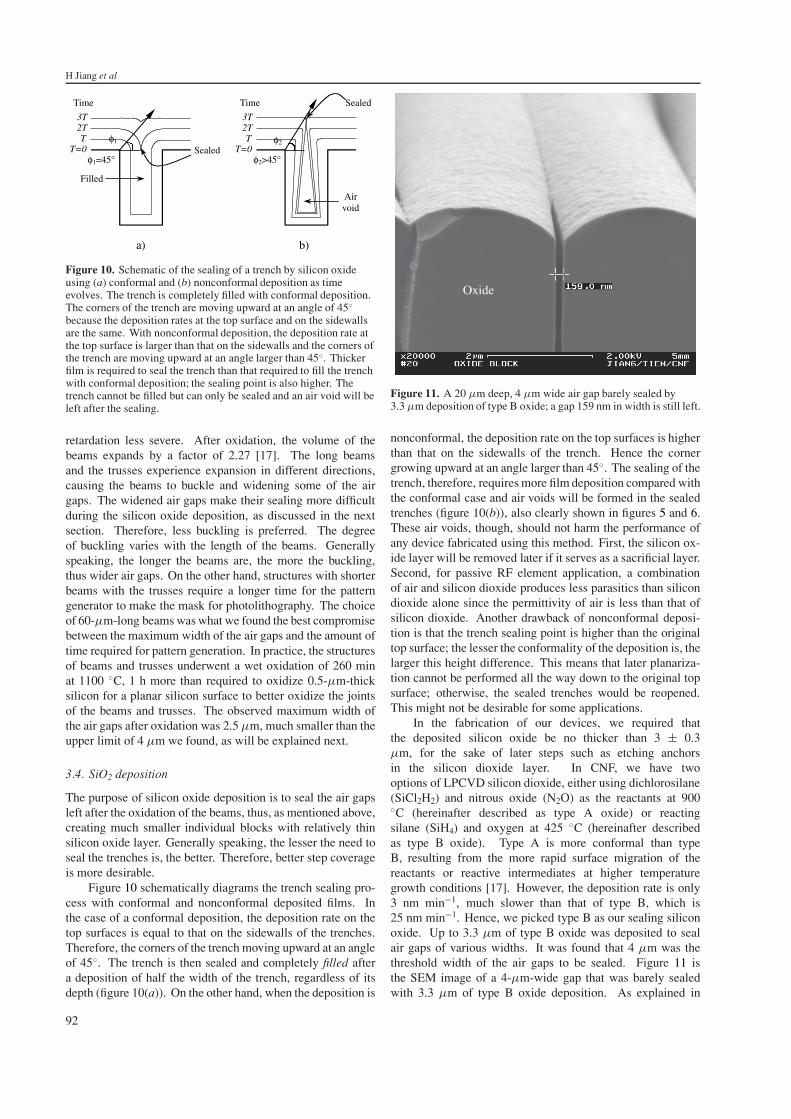
Oxide
Figure 11. A 20 µm deep, 4 µm wide air gap barely sealed by3.3 µm deposition of type B oxide; a gap 159 nm in width is still left.
nonconformal, the deposition rate on the top surfaces is higherthan that on the sidewalls of the trench. Hence the cornergrowing upward at an angle larger than 45◦. The sealing of thetrench, therefore, requires more film deposition compared withthe conformal case and air voids will be formed in the sealedtrenches (figure 10(b)), also clearly shown in figures 5 and 6.These air voids, though, should not harm the performance ofany device fabricated using this method. First, the silicon ox-ide layer will be removed later if it serves as a sacrificial layer.Second, for passive RF element application, a combinationof air and silicon dioxide produces less parasitics than silicondioxide alone since the permittivity of air is less than that ofsilicon dioxide. Another drawback of nonconformal deposi-tion is that the trench sealing point is higher than the originaltop surface; the lesser the conformality of the deposition is, thelarger this height difference. This means that later planariza-tion cannot be performed all the way down to the original topsurface; otherwise, the sealed trenches would be reopened.This might not be desirable for some applications.
In the fabrication of our devices, we required thatthe deposited silicon oxide be no thicker than 3 ± 0.3µm, for the sake of later steps such as etching anchorsin the silicon dioxide layer. In CNF, we have twooptions of LPCVD silicon dioxide, either using dichlorosilane(SiCl2H2) and nitrous oxide (N2O) as the reactants at 900◦C (hereinafter described as type A oxide) or reactingsilane (SiH4) and oxygen at 425 ◦C (hereinafter describedas type B oxide). Type A is more conformal than typeB, resulting from the more rapid surface migration of thereactants or reactive intermediates at higher temperaturegrowth conditions [17]. However, the deposition rate is only3 nm min−1, much slower than that of type B, which is25 nm min−1. Hence, we picked type B as our sealing siliconoxide. Up to 3.3 µm of type B oxide was deposited to sealair gaps of various widths. It was found that 4 µm was thethreshold width of the air gaps to be sealed. Figure 11 isthe SEM image of a 4-µm-wide gap that was barely sealedwith 3.3 µm of type B oxide deposition. As explained in
92
Fabrication of thick silicon dioxide sacrificial and isolation blocks
the previous section, the maximum width of the air gaps afterthe oxidation of our beam-and-truss structures was 2.5 µm,smaller than the 4 µm limit. In practice we deposited 3 µmof type B oxide in order to get as thick an insulating film aspossible and to leave more tolerance for the CMP step, whichwill thin down the silicon oxide layer.
4. Applications
In this section we demonstrate the applications of the processmodule to form thick silicon oxide blocks described above. Inthe first two examples, the block served as an underlying large-area isolation layer, while in the last two, it was a sacrificialblock that enabled the integration of polysilicon surface- andsingle-crystal bulk micromachining.
4.1. A tunable capacitor
The first example is an on-chip tunable capacitor. It consistsof two polysilicon plates, one fixed and one suspended bysprings, separated by a silicon oxide sacrificial layer. Thedevice is fabricated on a 20-µm-thick silicon dioxide block.The polysilicon plates will later be plated with copper afterthe removal of the sacrificial oxide for high conductivity[20]. When a voltage is applied between the two plates,the suspended plate will be attracted toward the fixed plate,thus changing the capacitance between the two plates. If thecapacitor is built on a thick silicon oxide layer, the parasiticcapacitances between the plates and the silicon substrate willbe drastically diminished.
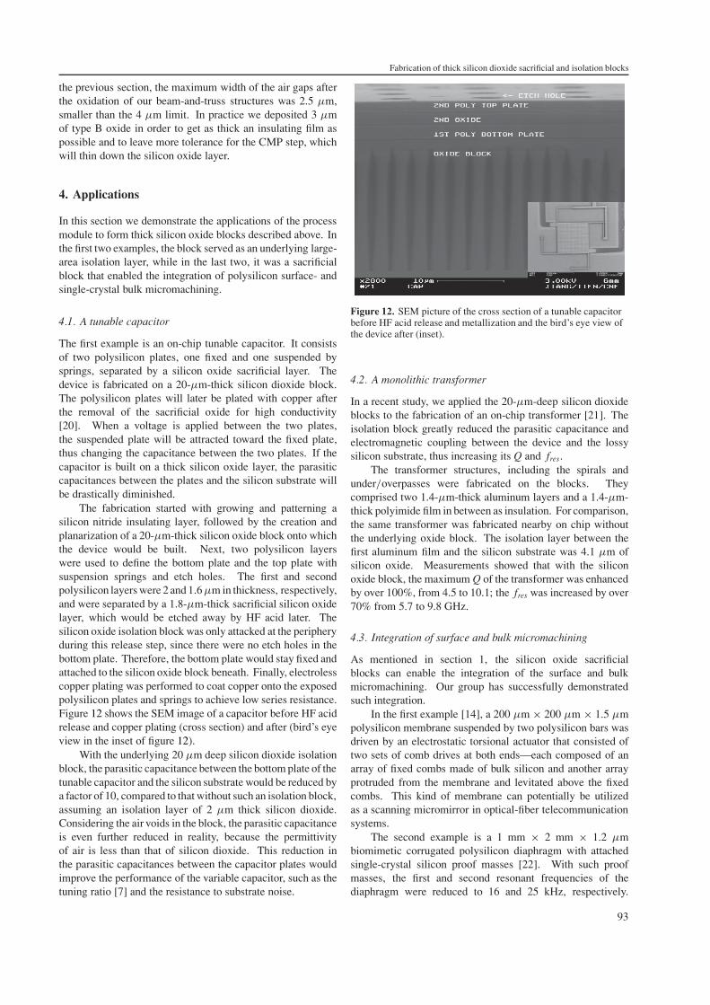
The fabrication started with growing and patterning asilicon nitride insulating layer, followed by the creation andplanarization of a 20-µm-thick silicon oxide block onto whichthe device would be built. Next, two polysilicon layerswere used to define the bottom plate and the top plate withsuspension springs and etch holes. The first and secondpolysilicon layers were 2 and 1.6 µm in thickness, respectively,and were separated by a 1.8-µm-thick sacrificial silicon oxidelayer, which would be etched away by HF acid later. Thesilicon oxide isolation block was only attacked at the peripheryduring this release step, since there were no etch holes in thebottom plate. Therefore, the bottom plate would stay fixed andattached to the silicon oxide block beneath. Finally, electrolesscopper plating was performed to coat copper onto the exposedpolysilicon plates and springs to achieve low series resistance.Figure 12 shows the SEM image of a capacitor before HF acidrelease and copper plating (cross section) and after (bird’s eyeview in the inset of figure 12).
With the underlying 20 µm deep silicon dioxide isolationblock, the parasitic capacitance between the bottom plate of thetunable capacitor and the silicon substrate would be reduced bya factor of 10, compared to that without such an isolation block,assuming an isolation layer of 2 µm thick silicon dioxide.Considering the air voids in the block, the parasitic capacitanceis even further reduced in reality, because the permittivityof air is less than that of silicon dioxide. This reduction inthe parasitic capacitances between the capacitor plates wouldimprove the performance of the variable capacitor, such as thetuning ratio [7] and the resistance to substrate noise.
Figure 12. SEM picture of the cross section of a tunable capacitorbefore HF acid release and metallization and the bird’s eye view ofthe device after (inset).
4.2. A monolithic transformer
In a recent study, we applied the 20-µm-deep silicon dioxideblocks to the fabrication of an on-chip transformer [21]. Theisolation block greatly reduced the parasitic capacitance andelectromagnetic coupling between the device and the lossysilicon substrate, thus increasing its Q and fres.
The transformer structures, including the spirals andunder/overpasses were fabricated on the blocks. Theycomprised two 1.4-µm-thick aluminum layers and a 1.4-µm-thick polyimide film in between as insulation. For comparison,the same transformer was fabricated nearby on chip withoutthe underlying oxide block. The isolation layer between thefirst aluminum film and the silicon substrate was 4.1 µm ofsilicon oxide. Measurements showed that with the siliconoxide block, the maximum Q of the transformer was enhancedby over 100%, from 4.5 to 10.1; the fres was increased by over70% from 5.7 to 9.8 GHz.
4.3. Integration of surface and bulk micromachining
As mentioned in section 1, the silicon oxide sacrificialblocks can enable the integration of the surface and bulkmicromachining. Our group has successfully demonstratedsuch integration.
In the first example [14], a 200 µm × 200 µm × 1.5 µmpolysilicon membrane suspended by two polysilicon bars wasdriven by an electrostatic torsional actuator that consisted oftwo sets of comb drives at both ends—each composed of anarray of fixed combs made of bulk silicon and another arrayprotruded from the membrane and levitated above the fixedcombs. This kind of membrane can potentially be utilizedas a scanning micromirror in optical-fiber telecommunicationsystems.
The second example is a 1 mm × 2 mm × 1.2 µmbiomimetic corrugated polysilicon diaphragm with attachedsingle-crystal silicon proof masses [22]. With such proofmasses, the first and second resonant frequencies of thediaphragm were reduced to 16 and 25 kHz, respectively.
93
H Jiang et al
Figure 13. SEM image of a corner of the tunable capacitor with anunderlying 20-µm-deep, 370 × 370 µm2-large silicon oxide block(not shown). The top polysilicon plate is suspended by springsanchored to the edges of the block. The flatness of the top plate andthe spring suggests that there is no apparent detrimental effect of theisolation block on the device structures.
Frequencies between these two resulted in the linearcombination of the two modes, producing an asymmetric shapeof the diaphragm corresponding to the direction of the acousticsource. The diaphragm can be applied to the fabrication ofdirectional hearing aids.
5. Discussion
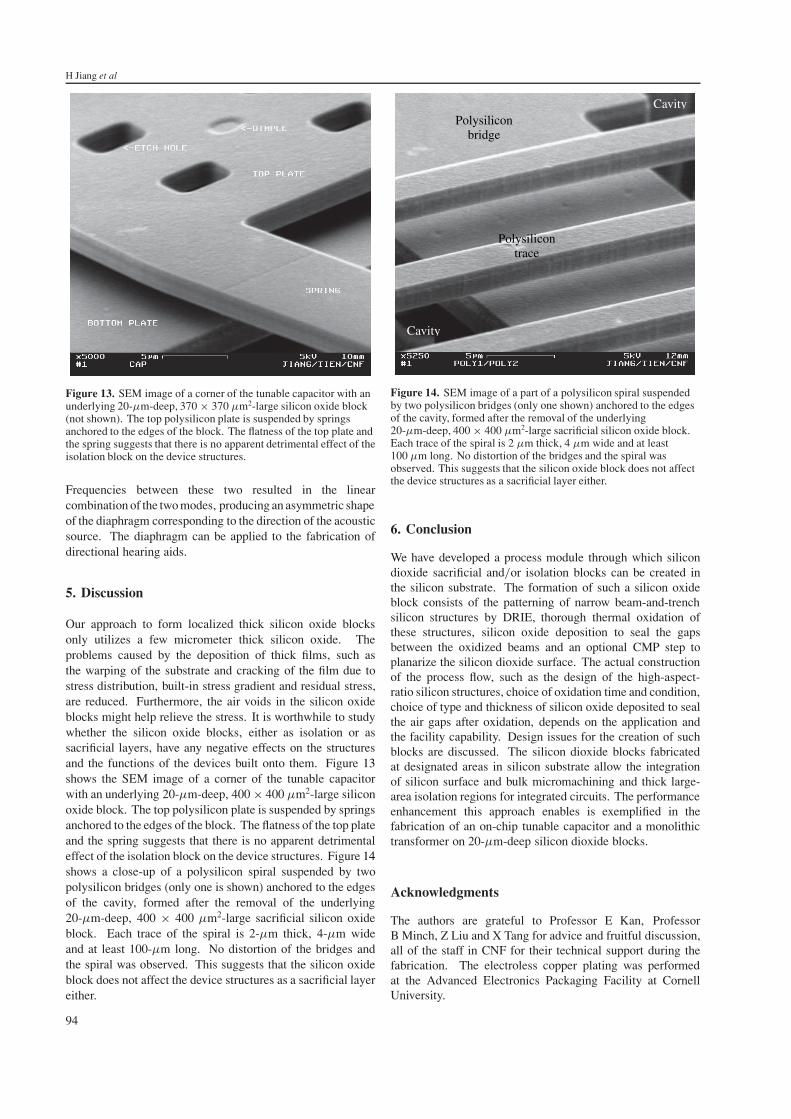
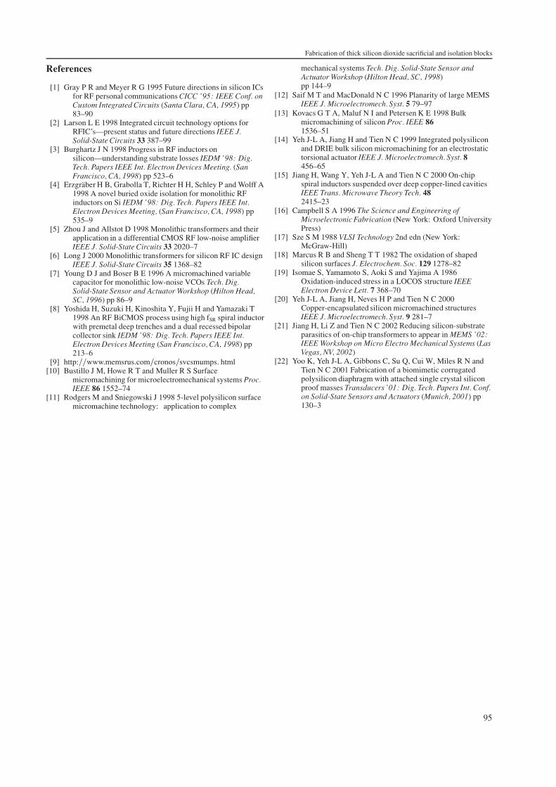
Our approach to form localized thick silicon oxide blocksonly utilizes a few micrometer thick silicon oxide. Theproblems caused by the deposition of thick films, such asthe warping of the substrate and cracking of the film due tostress distribution, built-in stress gradient and residual stress,are reduced. Furthermore, the air voids in the silicon oxideblocks might help relieve the stress. It is worthwhile to studywhether the silicon oxide blocks, either as isolation or assacrificial layers, have any negative effects on the structuresand the functions of the devices built onto them. Figure 13shows the SEM image of a corner of the tunable capacitorwith an underlying 20-µm-deep, 400 × 400 µm2-large siliconoxide block. The top polysilicon plate is suspended by springsanchored to the edges of the block. The flatness of the top plateand the spring suggests that there is no apparent detrimentaleffect of the isolation block on the device structures. Figure 14shows a close-up of a polysilicon spiral suspended by twopolysilicon bridges (only one is shown) anchored to the edgesof the cavity, formed after the removal of the underlying20-µm-deep, 400 × 400 µm2-large sacrificial silicon oxideblock. Each trace of the spiral is 2-µm thick, 4-µm wideand at least 100-µm long. No distortion of the bridges andthe spiral was observed. This suggests that the silicon oxideblock does not affect the device structures as a sacrificial layereither.
Polysiliconbridge
Polysilicontrace
Cavity
Cavity
Figure 14. SEM image of a part of a polysilicon spiral suspendedby two polysilicon bridges (only one shown) anchored to the edgesof the cavity, formed after the removal of the underlying20-µm-deep, 400 × 400 µm2-large sacrificial silicon oxide block.Each trace of the spiral is 2 µm thick, 4 µm wide and at least100 µm long. No distortion of the bridges and the spiral wasobserved. This suggests that the silicon oxide block does not affectthe device structures as a sacrificial layer either.
6. Conclusion
We have developed a process module through which silicondioxide sacrificial and/or isolation blocks can be created inthe silicon substrate. The formation of such a silicon oxideblock consists of the patterning of narrow beam-and-trenchsilicon structures by DRIE, thorough thermal oxidation ofthese structures, silicon oxide deposition to seal the gapsbetween the oxidized beams and an optional CMP step toplanarize the silicon dioxide surface. The actual constructionof the process flow, such as the design of the high-aspect-ratio silicon structures, choice of oxidation time and condition,choice of type and thickness of silicon oxide deposited to sealthe air gaps after oxidation, depends on the application andthe facility capability. Design issues for the creation of suchblocks are discussed. The silicon dioxide blocks fabricatedat designated areas in silicon substrate allow the integrationof silicon surface and bulk micromachining and thick large-area isolation regions for integrated circuits. The performanceenhancement this approach enables is exemplified in thefabrication of an on-chip tunable capacitor and a monolithictransformer on 20-µm-deep silicon dioxide blocks.
Acknowledgments
The authors are grateful to Professor E Kan, ProfessorB Minch, Z Liu and X Tang for advice and fruitful discussion,all of the staff in CNF for their technical support during thefabrication. The electroless copper plating was performedat the Advanced Electronics Packaging Facility at CornellUniversity.
94
Fabrication of thick silicon dioxide sacrificial and isolation blocks
References
[1] Gray P R and Meyer R G 1995 Future directions in silicon ICsfor RF personal communications CICC ’95: IEEE Conf. onCustom Integrated Circuits (Santa Clara, CA, 1995) pp83–90
[2] Larson L E 1998 Integrated circuit technology options forRFIC’s—present status and future directions IEEE J.Solid-State Circuits 33 387–99
[3] Burghartz J N 1998 Progress in RF inductors onsilicon—understanding substrate losses IEDM ’98: Dig.Tech. Papers IEEE Int. Electron Devices Meeting. (SanFrancisco, CA, 1998) pp 523–6
[4] Erzgraber H B, Grabolla T, Richter H H, Schley P and Wolff A1998 A novel buried oxide isolation for monolithic RFinductors on Si IEDM ’98: Dig. Tech. Papers IEEE Int.Electron Devices Meeting, (San Francisco, CA, 1998) pp535–9
[5] Zhou J and Allstot D 1998 Monolithic transformers and theirapplication in a differential CMOS RF low-noise amplifierIEEE J. Solid-State Circuits 33 2020–7
[6] Long J 2000 Monolithic transformers for silicon RF IC designIEEE J. Solid-State Circuits 35 1368–82
[7] Young D J and Boser B E 1996 A micromachined variablecapacitor for monolithic low-noise VCOs Tech. Dig.Solid-State Sensor and Actuator Workshop (Hilton Head,SC, 1996) pp 86–9
[8] Yoshida H, Suzuki H, Kinoshita Y, Fujii H and Yamazaki T1998 An RF BiCMOS process using high fSR spiral inductorwith premetal deep trenches and a dual recessed bipolarcollector sink IEDM ’98: Dig. Tech. Papers IEEE Int.Electron Devices Meeting (San Francisco, CA, 1998) pp213–6
[9] http://www.memsrus.com/cronos/svcsmumps. html[10] Bustillo J M, Howe R T and Muller R S Surface
micromachining for microelectromechanical systems Proc.IEEE 86 1552–74
[11] Rodgers M and Sniegowski J 1998 5-level polysilicon surfacemicromachine technology: application to complex
mechanical systems Tech. Dig. Solid-State Sensor andActuator Workshop (Hilton Head, SC, 1998)pp 144–9
[12] Saif M T and MacDonald N C 1996 Planarity of large MEMSIEEE J. Microelectromech. Syst. 5 79–97
[13] Kovacs G T A, Maluf N I and Petersen K E 1998 Bulkmicromachining of silicon Proc. IEEE 861536–51
[14] Yeh J-L A, Jiang H and Tien N C 1999 Integrated polysiliconand DRIE bulk silicon micromachining for an electrostatictorsional actuator IEEE J. Microelectromech. Syst. 8456–65
[15] Jiang H, Wang Y, Yeh J-L A and Tien N C 2000 On-chipspiral inductors suspended over deep copper-lined cavitiesIEEE Trans. Microwave Theory Tech. 482415–23
[16] Campbell S A 1996 The Science and Engineering ofMicroelectronic Fabrication (New York: Oxford UniversityPress)
[17] Sze S M 1988 VLSI Technology 2nd edn (New York:McGraw-Hill)
[18] Marcus R B and Sheng T T 1982 The oxidation of shapedsilicon surfaces J. Electrochem. Soc. 129 1278–82
[19] Isomae S, Yamamoto S, Aoki S and Yajima A 1986Oxidation-induced stress in a LOCOS structure IEEEElectron Device Lett. 7 368–70
[20] Yeh J-L A, Jiang H, Neves H P and Tien N C 2000Copper-encapsulated silicon micromachined structuresIEEE J. Microelectromech. Syst. 9 281–7
[21] Jiang H, Li Z and Tien N C 2002 Reducing silicon-substrateparasitics of on-chip transformers to appear in MEMS ’02:IEEE Workshop on Micro Electro Mechanical Systems (LasVegas, NV, 2002)
[22] Yoo K, Yeh J-L A, Gibbons C, Su Q, Cui W, Miles R N andTien N C 2001 Fabrication of a biomimetic corrugatedpolysilicon diaphragm with attached single crystal siliconproof masses Transducers ’01: Dig. Tech. Papers Int. Conf.on Solid-State Sensors and Actuators (Munich, 2001) pp130–3
95


![MAXPROLOGIC FPGA DEVELOPMENT SYSTEM Data Sheet€¦ · J4-6 XIO8_5 102 XIO8[5] J4-7 XIO8_6 105 XIO8[6] J4-8 XIO8_7 106 XIO8[7] J4-9 GND NC NC J4-10 GND NC NC Connector-Pin # Net Name](https://img.pdfslide.us/doc/110x75/609406a89a61bb3a6e6a0473/maxprologic-fpga-development-system-data-sheet-j4-6-xio85-102-xio85-j4-7-xio86.jpg)