Embed Size (px)
Citation preview
1
12Crystal-Growth Technology for Ternary III-V SemiconductorProduction by Vertical Bridgman and Vertical Gradient FreezingMethods with Accelerated Crucible Rotation Technique
P.S. Dutta
12.1Introduction
In semiconductor device technology, multilayered thin-film structures comprisingvarious ternary and quaternary compounds are grown on binary substrates usingliquid phase epitaxy (LPE), metal-organic vapor phase epitaxy (MOCVD or OMVPE)or molecular beam epitaxy (MBE) techniques [1–5]. Due to the lattice mismatchbetween the epilayer and the substrate, misfit dislocations originate at the growthinterface and propagate into the device layers [6]. Typical misfit dislocation densitiesare in the range of 106 –109 cm−2 [6]. Such high density of dislocations leads todegradation of electrical and optical characteristics of the devices. To reducethe misfit dislocation density, a variety of buffer layers are grown between thesubstrate and the device layers. The buffer-layer technology necessary to relievemisfit-related stresses is not optimized for all systems and often devices exhibitpoor characteristics due to interfacial defects. By using lattice-matched ternarysubstrates, enhancement in performances of electronic and optoelectronic deviceshas already been demonstrated [7–16]. However, bulk single-crystal substratesof ternary semiconductors are still not available for commercial applications dueto inherent problems in growing them from the melt [17–31]. The high costof ternary wafers due to poor yield of the substrates grown from melt with thesame alloy composition has restricted their usage in commercial semiconductordevices. This chapter lays out the challenges and potential solutions that couldbe adopted for future commercial development of ternary substrates. We willfirst discuss the fundamental issues encountered during ternary crystal growthand then present a process developed in our group to meet the requirements forlarge-diameter homogeneous ternary crystal growth. The crystal-growth methodis a combination of vertical Bridgman or vertical gradient freezing techniquewith accelerated crucible rotation technique and a periodic solute-feeding process[32–34]. The optimization of the growth parameters to obtain compositionallyhomogeneous wafers of 50-mm diameter GaInSb with high yield will be discussed.
Crystal Growth Technology. Edited by Hans J. Scheel and Peter CapperCopyright 2008 WILEY-VCH Verlag GmbH & Co. KGaA, WeinheimISBN: 978-3-527-31762-2
2 12 Crystal-Growth Technology for Ternary III-V Semiconductor Production
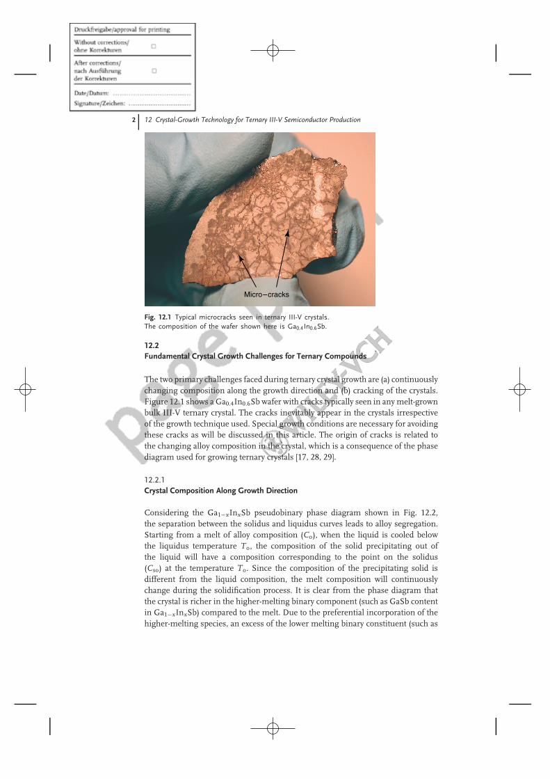
Micro–cracks
Fig. 12.1 Typical microcracks seen in ternary III-V crystals.The composition of the wafer shown here is Ga0.4In0.6Sb.
12.2Fundamental Crystal Growth Challenges for Ternary Compounds
The two primary challenges faced during ternary crystal growth are (a) continuouslychanging composition along the growth direction and (b) cracking of the crystals.Figure 12.1 shows a Ga0.4In0.6Sb wafer with cracks typically seen in any melt-grownbulk III-V ternary crystal. The cracks inevitably appear in the crystals irrespectiveof the growth technique used. Special growth conditions are necessary for avoidingthese cracks as will be discussed in this article. The origin of cracks is related tothe changing alloy composition in the crystal, which is a consequence of the phasediagram used for growing ternary crystals [17, 28, 29].
12.2.1Crystal Composition Along Growth Direction
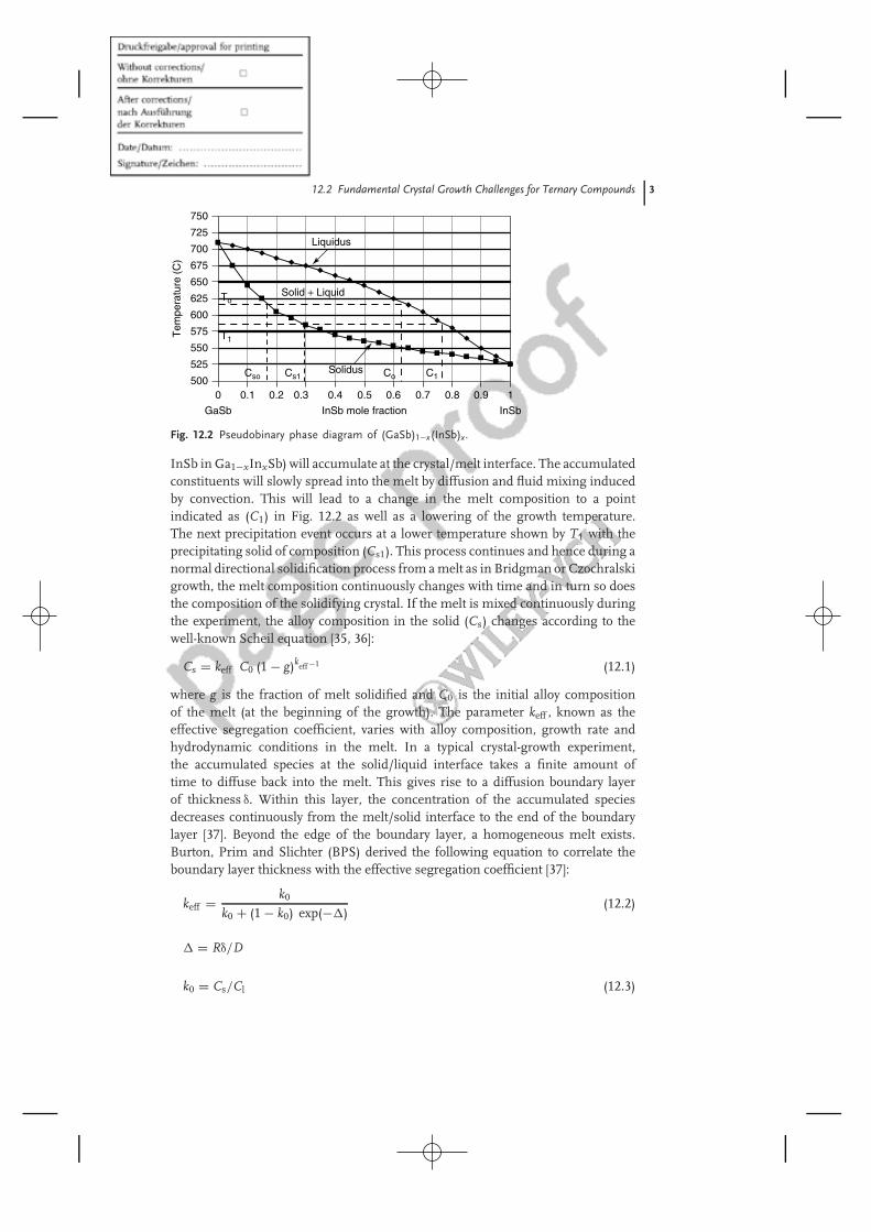
Considering the Ga1−xInxSb pseudobinary phase diagram shown in Fig. 12.2,the separation between the solidus and liquidus curves leads to alloy segregation.Starting from a melt of alloy composition (Co), when the liquid is cooled belowthe liquidus temperature To, the composition of the solid precipitating out ofthe liquid will have a composition corresponding to the point on the solidus(Cso) at the temperature To. Since the composition of the precipitating solid isdifferent from the liquid composition, the melt composition will continuouslychange during the solidification process. It is clear from the phase diagram thatthe crystal is richer in the higher-melting binary component (such as GaSb contentin Ga1−xInxSb) compared to the melt. Due to the preferential incorporation of thehigher-melting species, an excess of the lower melting binary constituent (such as
12.2 Fundamental Crystal Growth Challenges for Ternary Compounds 3
500
525
550
575
600
625
650
675
700
725
750
0 0.1 0.2 0.3 0.4 0.5 0.6 0.7 0.8 0.9 1
InSb mole fraction
Tem
pera
ture
(C
)
Solid + Liquid
Liquidus
Solidus
GaSb InSb
Co C1Cso Cs1
To
T1
Fig. 12.2 Pseudobinary phase diagram of (GaSb)1−x(InSb)x.
InSb in Ga1−xInxSb) will accumulate at the crystal/melt interface. The accumulatedconstituents will slowly spread into the melt by diffusion and fluid mixing inducedby convection. This will lead to a change in the melt composition to a pointindicated as (C1) in Fig. 12.2 as well as a lowering of the growth temperature.The next precipitation event occurs at a lower temperature shown by T1 with theprecipitating solid of composition (Cs1). This process continues and hence during anormal directional solidification process from a melt as in Bridgman or Czochralskigrowth, the melt composition continuously changes with time and in turn so doesthe composition of the solidifying crystal. If the melt is mixed continuously duringthe experiment, the alloy composition in the solid (Cs) changes according to thewell-known Scheil equation [35, 36]:
Cs = keff C0 (1 − g)keff −1 (12.1)
where g is the fraction of melt solidified and C0 is the initial alloy compositionof the melt (at the beginning of the growth). The parameter keff , known as theeffective segregation coefficient, varies with alloy composition, growth rate andhydrodynamic conditions in the melt. In a typical crystal-growth experiment,the accumulated species at the solid/liquid interface takes a finite amount oftime to diffuse back into the melt. This gives rise to a diffusion boundary layerof thickness δ. Within this layer, the concentration of the accumulated speciesdecreases continuously from the melt/solid interface to the end of the boundarylayer [37]. Beyond the edge of the boundary layer, a homogeneous melt exists.Burton, Prim and Slichter (BPS) derived the following equation to correlate theboundary layer thickness with the effective segregation coefficient [37]:
keff = k0
k0 + (1 − k0) exp(−∆)(12.2)
∆ = Rδ/D
k0 = Cs/Cl (12.3)
4 12 Crystal-Growth Technology for Ternary III-V Semiconductor Production
where k0 is the equilibrium segregation coefficient as estimated from the ratioof solidus concentration (Cs) and liquidus concentration (Cl) of any constituentat a given temperature in the phase diagram (see Fig. 12.2). D is the diffusioncoefficient of the accumulated species at the melt/solid interface and R is the crystalgrowth rate. The diffusion coefficient D is a fundamental material property and isdependent on the alloy composition as well as the temperature. For example, thediffusion coefficient of InSb in Ga1−xInxSb melt at 600 ◦C is lower than that at650 ◦C. Similarly, the diffusion coefficient of InSb in a Ga melt at 600 ◦C is differentfrom that in a Ga1−xInxSb melt at the same temperature.
In the presence of forced convection in the melt, the boundary layer thickness, δ,can be approximately estimated by:
δ = 1.6D1/3ν1/6�−1/2 (12.4)
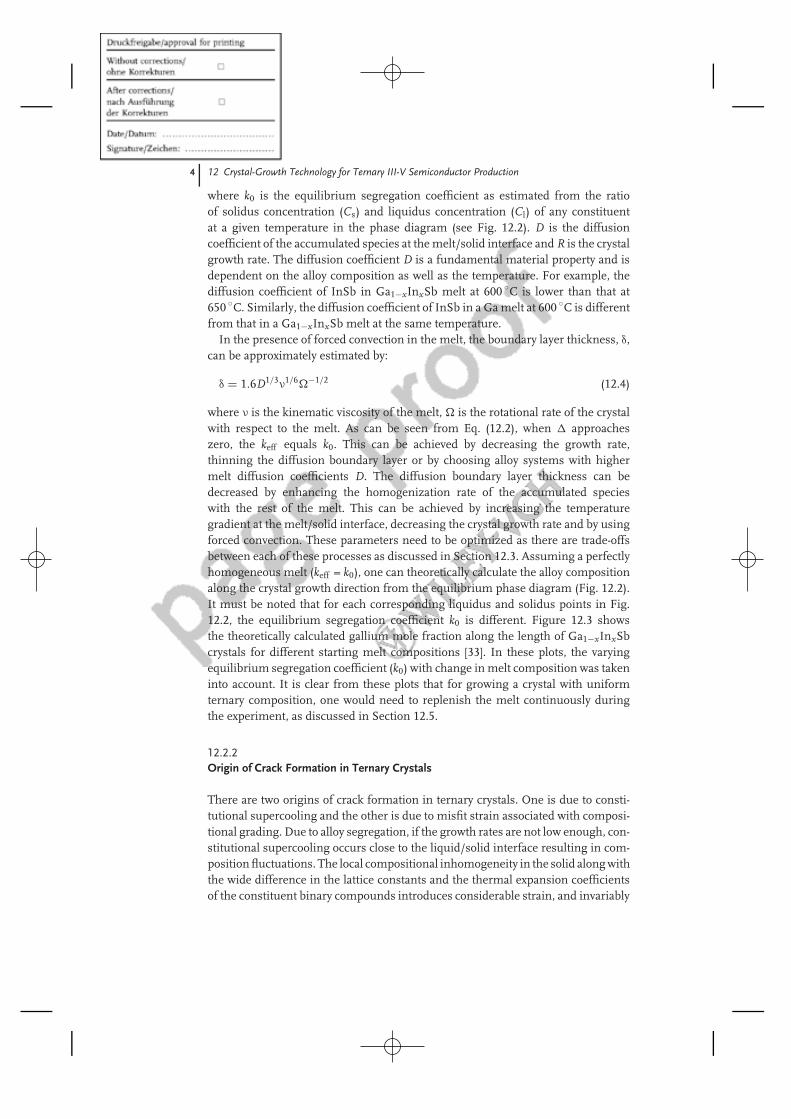
where ν is the kinematic viscosity of the melt, � is the rotational rate of the crystalwith respect to the melt. As can be seen from Eq. (12.2), when ∆ approacheszero, the keff equals k0. This can be achieved by decreasing the growth rate,thinning the diffusion boundary layer or by choosing alloy systems with highermelt diffusion coefficients D. The diffusion boundary layer thickness can bedecreased by enhancing the homogenization rate of the accumulated specieswith the rest of the melt. This can be achieved by increasing the temperaturegradient at the melt/solid interface, decreasing the crystal growth rate and by usingforced convection. These parameters need to be optimized as there are trade-offsbetween each of these processes as discussed in Section 12.3. Assuming a perfectlyhomogeneous melt (keff = k0), one can theoretically calculate the alloy compositionalong the crystal growth direction from the equilibrium phase diagram (Fig. 12.2).It must be noted that for each corresponding liquidus and solidus points in Fig.12.2, the equilibrium segregation coefficient k0 is different. Figure 12.3 showsthe theoretically calculated gallium mole fraction along the length of Ga1−xInxSbcrystals for different starting melt compositions [33]. In these plots, the varyingequilibrium segregation coefficient (k0) with change in melt composition was takeninto account. It is clear from these plots that for growing a crystal with uniformternary composition, one would need to replenish the melt continuously duringthe experiment, as discussed in Section 12.5.
12.2.2Origin of Crack Formation in Ternary Crystals
There are two origins of crack formation in ternary crystals. One is due to consti-tutional supercooling and the other is due to misfit strain associated with composi-tional grading. Due to alloy segregation, if the growth rates are not low enough, con-stitutional supercooling occurs close to the liquid/solid interface resulting in com-position fluctuations. The local compositional inhomogeneity in the solid along withthe wide difference in the lattice constants and the thermal expansion coefficientsof the constituent binary compounds introduces considerable strain, and invariably
12.2 Fundamental Crystal Growth Challenges for Ternary Compounds 5
1
0.9
0.8
0.7
0.6
0.5
0.4
0.3
0.2
0.1
0
Gal
lium
mol
e fr
actio
n
0.1
0.3
0.50.7
0.9
0 0.2 0.4 0.6 0.8 1
Fraction solidified (G)
Fig. 12.3 Theoretical gallium concentration along the growthaxis for GaxIn1−xSb crystals grown from different startingmelt compositions (under normal freezing conditions). Thefractions next to each curve represent the gallium mole frac-tion in the starting melt.
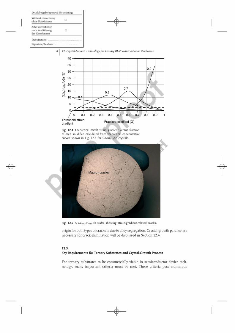
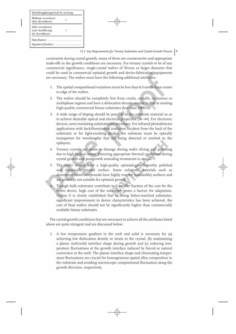
leads to cracking of the crystals. Cracking in the crystal can also occur without con-stitutional supercooling. These cracks are due to misfit strain in the crystal and arerelated to the rate at which the alloy composition and more importantly the latticeparameter and other physical properties like thermal expansion coefficient changesalong the length of the crystal. For the GaInSb system, the lattice parameter variesfrom 6.096 A (for GaSb) to 6.479 A (for InSb) and the thermal expansion coefficientfrom 7.75 × 10⁻⁶ ◦C−1 to 5.37 × 10⁻⁶ ◦C−1 [1]. Figure 12.4 shows the theoreticalmisfit strain-gradient curves calculated using the theoretical alloy composition pro-files shown in Fig. 12.3 and the lattice parameter a0 for each composition using theVegard’s law [1]. It has been empirically observed that crystals inevitably crack if themisfit strain gradient exceeds 1–2% [17]. It is obvious that an alloy system with largerseparation between the solidus and liquidus curves will have higher strain gradientthan those with smaller separation. Moreover, cracking may occur even below 1%of misfit strain gradient if there is a thermal strain due to a large temperature gra-dient in the solid during growth and during postgrowth cooling. Figure 12.5 showstypical misfit strain-gradient related cracks in a Ga0.95In0.05Sb polycrystal wafergrown using the vertical Bridgman method. Referring to Fig. 12.5, the strain-relatedcracks originate in the crystal where the strain gradient exceeds 1–2%, as shown bythe horizontal dashed line. For a crystal grown with a starting gallium mole fractionof 0.7 in the melt, the cracks should appear when the fraction solidified (G) reaches25%. The highest probability for cracking has been experimentally observed aroundthe peak of the strain gradient [32], which is close to 60% for the melt with 0.7 start-ing gallium mole fraction. The visual appearance of the supercooling-related cracks(shown in Fig. 12.1) and that of misfit strain-gradient-related cracks (Fig. 12.5)are quite different and can be easily distinguished. Nevertheless, the fundamental
6 12 Crystal-Growth Technology for Ternary III-V Semiconductor Production
0
5
10
15
20
25
30
35
40
0 0.1 0.2 0.3 0.4 0.5 0.6 0.7 0.8 0.9 1
(1/a
o)(d
a o/d
G)
[%]
Fraction solidified (G)
0.1
0.30.7
0.9
Threshold straingradient
Fig. 12.4 Theoretical misfit strain gradient versus fractionof melt solidified calculated from theoretical concentrationcurves shown in Fig. 12.3 for GaxIn1−xSb crystals.
Macro–cracks
Fig. 12.5 A Ga0.95In0.05Sb wafer showing strain-gradient-related cracks.
origin for both types of cracks is due to alloy segregation. Crystal-growth parametersnecessary for crack elimination will be discussed in Section 12.4.
12.3Key Requirements for Ternary Substrates and Crystal-Growth Process
For ternary substrates to be commercially viable in semiconductor device tech-nology, many important criteria must be met. These criteria pose numerous
12.3 Key Requirements for Ternary Substrates and Crystal-Growth Process 7
constraints during crystal growth, many of them are counteractive and appropriatetrade-offs in the growth conditions are necessary. For ternary crystals to be of anycommercial significance, single-crystal wafers of 50 mm or larger diameter thatcould be used in commercial epitaxial growth and device-fabrication equipmentsare necessary. The wafers must have the following additional attributes:
1. The spatial compositional variations must be less than 0.5 mol% from centerto edge of the wafers.
2. The wafers should be completely free from cracks, metallic inclusions ormultiphase regions and have a dislocation density similar to that in existinghigh-quality commercial binary substrates (less than 1000 cm−2).
3. A wide range of doping should be possible in the substrate material so asto achieve desirable optical and electrical properties [38–44]. For electronicdevices, semi-insulating substrates are necessary. For infrared photodetectorapplications with backillumination (radiation incident from the back of thesubstrate) or for light-emitting diodes, the substrate must be opticallytransparent for wavelengths that are being detected or emitted in theepilayers.
4. Ternary crystals are prone to damage during wafer slicing and polishingdue to high built-in strain. Ensuring appropriate thermal conditions duringcrystal growth and postgrowth annealing treatments is crucial.
5. The wafer should have a high-quality epitaxial-growth-worthy polishedand chemically treated surface. Some substrate materials such asaluminum-based compounds have highly reactive (oxidizable) surfaces andare generally not suitable for epitaxial growth.
6. Though bulk substrates contribute to a smaller fraction of the cost for theentire device, high cost of the substrates poses a barrier for adaptation.Unless it is clearly established that by using lattice-matched substrates,significant improvement in device characteristics has been achieved, thecost of final wafers should not be significantly higher than commerciallyavailable binary substrates.
The crystal-growth conditions that are necessary to achieve all the attributes listedabove are quite stringent and are discussed below:
1. A low temperature gradient in the melt and solid is necessary for (a)achieving low dislocation density or strain in the crystal, (b) maintaininga planar melt/solid interface shape during growth and (c) reducing tem-perature fluctuations at the growth interface induced by forced or naturalconvection in the melt. The planar interface shape and eliminating temper-ature fluctuations are crucial for homogeneous spatial alloy composition inthe substrate and avoiding microscopic compositional fluctuation along thegrowth direction, respectively.
8 12 Crystal-Growth Technology for Ternary III-V Semiconductor Production
2. A low temperature gradient, however, enhances the probability for constitu-tional supercooling. To avoid supercooling, the crystal growth rate must bereduced. But lower growth rate translates to higher final wafer cost. Hence,for maintaining reasonable growth rate (without supercooling) under a lowtemperature gradient, forced convection in the melt such as using ACRT isnecessary.
3. To lower substrate costs, it is also essential to have high yield of wafersof the same composition from a single ingot. This requires maintaining ahomogeneous melt composition during the entire growth by replenishingthe depleted constituents (solute feeding) in the melt. The solute dissolutionand feeding process must be augmented by appropriate melt stirring toensure a homogeneous melt at all times. Under a low temperature gradient,the natural convection is not strong enough to transport species effectivelyto and from the growth interface, thus leading to macroscopic compositionfluctuations along the growth direction.
4. Rapid or uncontrolled melt replenishment leads to high level of super-saturation in the melt. This triggers polycrystalline growth due to randomnucleation in the melt especially under a low temperature gradient. To main-tain single crystallinity during growth, the rate at which the solute is fed tothe melt must be precisely controlled at all times to match the crystal growthrate. This requires special solute-feeding processes and forced convectivemixing in the melt.
In summary, the three main parameters that are desirable for crystal growthof ternary alloys are: (a) low temperature gradient, (b) melt stirring by forcedconvection and (c) a precise solute dissolution process. Since large-diameterwafers are necessary for commercial applications, scaling up the production wouldrequire a crystal-growth process where optimization of the heat and mass transportis relatively easy to implement. The Bridgman and gradient freezing type methodsare becoming more popular for large-diameter binary crystal growth with verylow defect content. Fortunately, these growth systems could be easily upgraded toincorporate ACRT and solute-feeding mechanisms and adopted for future ternarycrystal-growth technology.
12.4Optimization of Growth Parameters for Radially Homogeneous Crystals
From the above discussions, it is apparent that optimization of melt homogenizationand solute-feeding processes in conjunction with the temperature gradient in themelt and solid is necessary for the successful growth of high-quality compositionallyhomogeneous ternary crystals. In this section, we will discuss the combinedeffects of axial temperature gradient and melt stirring using ACRT on the radialcompositional profile in ternary crystals.
12.4 Optimization of Growth Parameters for Radially Homogeneous Crystals 9
12.4.1Melt Homogenization Using ACRT
The role of melt stirring during ternary crystal growth is crucial. There are manyways for achieving melt stirring such as by using magnetic fields [45], stirrers andbaffles in the melt [25, 28, 32–34] and ACRT [28, 32–34, 46–51]. In this chapter,we will focus the discussion on ACRT due to its ease in adoptability for large-sizemelts as well as for sealed crucible configurations.
Due to the fact that ternary crystals need to be grown under low temperaturegradient, melt stirring during growth becomes very important and necessary formany purposes:
1. It helps transporting accumulated constituents from the melt/solid interfaceto the bulk melt by thinning the diffusion boundary layer. This helpsin maintaining a reasonable growth rate that is necessary for large-scaleproduction.
2. It helps the solute dissolution during the solute-feeding process (as discussedlater). In the absence of forced convection and with a low temperaturegradient in the melt, it takes a long time for the accumulated species (atthe melt/solid interface) to thoroughly mix with the bulk melt. Hence thesupersaturation level in the melt does not change, which results in nodissolution of the solute. Forced convection helps in rapid homogenizationof the melt and thus an efficient solute dissolution process could be achieved.
3. It helps in avoiding random nucleation in the growth melt as well asconstitutional supercooling at the growth interface. The latter helps ineliminating cracks in the crystal that originate from interface breakdown.
One of the primary goals during ternary crystal growth is to identify growthconditions that could eliminate cracks in the crystal. ACRT has been found tobe very efficient in eliminating the constitutional-supercooling-related cracks inlarge-diameter crystals [28, 32–34, 51]. To stress the importance of ACRT for crackelimination, let us review the theoretical analysis of Tiller et al. [52] for preventingconstitutional supercooling. According to this analysis, the ratio of temperaturegradient in the melt near the growth interface (G) to the growth rate (R) shouldexceed a critical value given by:
G
R≥ mC0(1 − k0)
k0 D(12.5)
where m is the slope of the liquidus in the phase diagram. While increasingthe axial temperature gradient helps in avoiding constitutional supercooling, itincreases the melt/solid interface curvature due to which the radial compositionprofile in the wafers varies (as discussed later). High axial temperature gradientalso lowers the threshold for strain-related cracks in the crystal, as discussedearlier and hence is not desirable. Hence, ternary crystals need to be grown undera low temperature gradient. To avoid constitutional supercooling under a lower
10 12 Crystal-Growth Technology for Ternary III-V Semiconductor Production
temperature gradient, the crystal growth rates necessary for crack-free crystals arevery low [28]. Such growth rates are not viable for commercial production. Theconstitutional supercooling can be avoided and the growth rate can be enhanced byappropriate melt stirring processes such as by ACRT. It must be noted that ACRThas no effect on the misfit-related cracks. These can be avoided only by ensuringa gradual change in alloy composition in the crystals during growth such as tomaintain the strain gradient below the threshold level (Fig. 12.4).
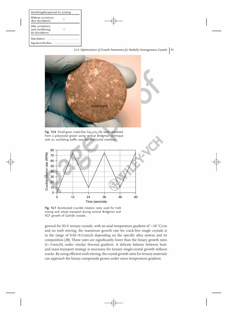
Fluid-mixing patterns used for forced convection could be very complicatedand significantly impacts the crystalline quality. Melt-mixing schemes reported inthe literature [25, 28, 32–34, 51] during ternary crystal growth include: unidirec-tional rotation of crucible, using baffles and stirrers and by accelerated cruciblerotation technique (ACRT). Unidirectional rotation even at higher rotation rates100–200 rpm does not result in effective mixing for large-diameter crystals (50 mmand higher). In the baffle-mixing scheme [25], the melt is homogenized very ef-ficiently either by rotating the baffle in the melt or by translating the baffle backand forth perpendicular to the growth interface. In the case where the baffle istranslated perpendicular to the growth interface, obtaining single crystals is quitedifficult due to thermal fluctuations at the melt/solid interface. Typically, very smallsized grains have been observed by using this process (Fig. 12.6). Nevertheless,it is worth mentioning that these wafers are compositionally homogeneous andno cracks are seen. Melt mixing using a stationary stirrer held inside the meltwhile the crucible is uniformly rotated in one direction has been found to be veryeffective in eliminating cracks as well as providing efficient solute transport duringsolute-feeding processes [32–34]. One of the limitations with any mixing processthat incorporates foreign object in the melt such as stirrer or baffle is that theheight of the melt needs to be deeper. For shallow melts, it is very difficult to usestirrers or baffles and avoid undesirable disturbances in the melt. ACRT is perfectlysuitable for melts of any size or depths and has been successfully used for ternarycrystal growth [28, 32–34, 51].
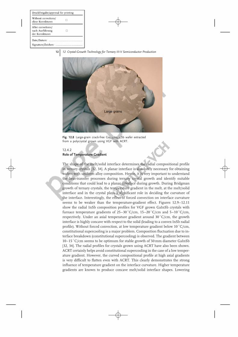
In ACRT, the crucible is periodically accelerated and de-accelerated (around thegrowth axis) to promote efficient mixing of the melt as shown in Fig. 12.7. However,there can be dead-zones (unmixed) even in a thoroughly mixed melt especially atthe center of the crystal [51]. This is specially seen in smaller-diameter crystals.These types of unmixed zones lead to compositional fluctuations in the growncrystals. Hence, it is essential to optimize the rotation schemes for each cruciblediameter, melt size and fluid viscosity in the ACRT scheme [46–50]. We haveobserved that by using ACRT, the growth rates of ternary III-V compounds canbe enhanced by a factor of 3–4. In vertical Bridgman grown crystals without anymelt stirring, typical growth rate necessary for obtaining crack-free GaInSb of anycomposition is less than 0.5 mm/h with axial temperature gradient of 10–15 ◦C/cm(near the melt/solid interface). By using optimized ACRT scheme as shown inFig. 12.7, the growth rate for crack-free crystals can be increased to 1.5–2 mm/hunder the same thermal gradient. Figure 12.8 shows a crack-free 50-mm diameterpolycrystalline wafer of Ga0.25In0.75Sb grown using the ACRT scheme. The growthrate was ∼1 mm/h similar to that used for the cracked wafer shown in Fig. 12.1. In
12.4 Optimization of Growth Parameters for Radially Homogeneous Crystals 11
Small grains
Fig. 12.6 Small-grain crack-free Ga0.8In0.2Sb wafer extractedfrom a polycrystal grown using vertical Bridgman techniquewith an oscillating baffle near the melt/solid interface.
00 12 24 36 48 60
10
20
30
40
50
60
70
80
Time (seconds)
Cru
cibl
e ro
tatio
n ra
te (
RP
M)
Fig. 12.7 Accelerated crucible rotation rates used for meltmixing and solute transport during vertical Bridgman andVGF growth of GaInSb crystals.
general for III-V ternary crystals, with an axial temperature gradient of ∼10 ◦C/cmand no melt stirring, the maximum growth rate for crack-free single crystals isin the range of 0.02–0.5 mm/h depending on the specific alloy system and itscomposition [28]. These rates are significantly lower than the binary growth rates(1–3 mm/h) under similar thermal gradient. A delicate balance between heat-and mass-transport strategy is necessary for ternary single-crystal growth withoutcracks. By using efficient melt stirring, the crystal growth rates for ternary materialscan approach the binary compounds grown under same temperature gradient.
12 12 Crystal-Growth Technology for Ternary III-V Semiconductor Production
Large grains
Fig. 12.8 Large-grain crack-free Ga0.25In0.75Sb wafer extractedfrom a polycrystal grown using VGF with ACRT.
12.4.2Role of Temperature Gradient
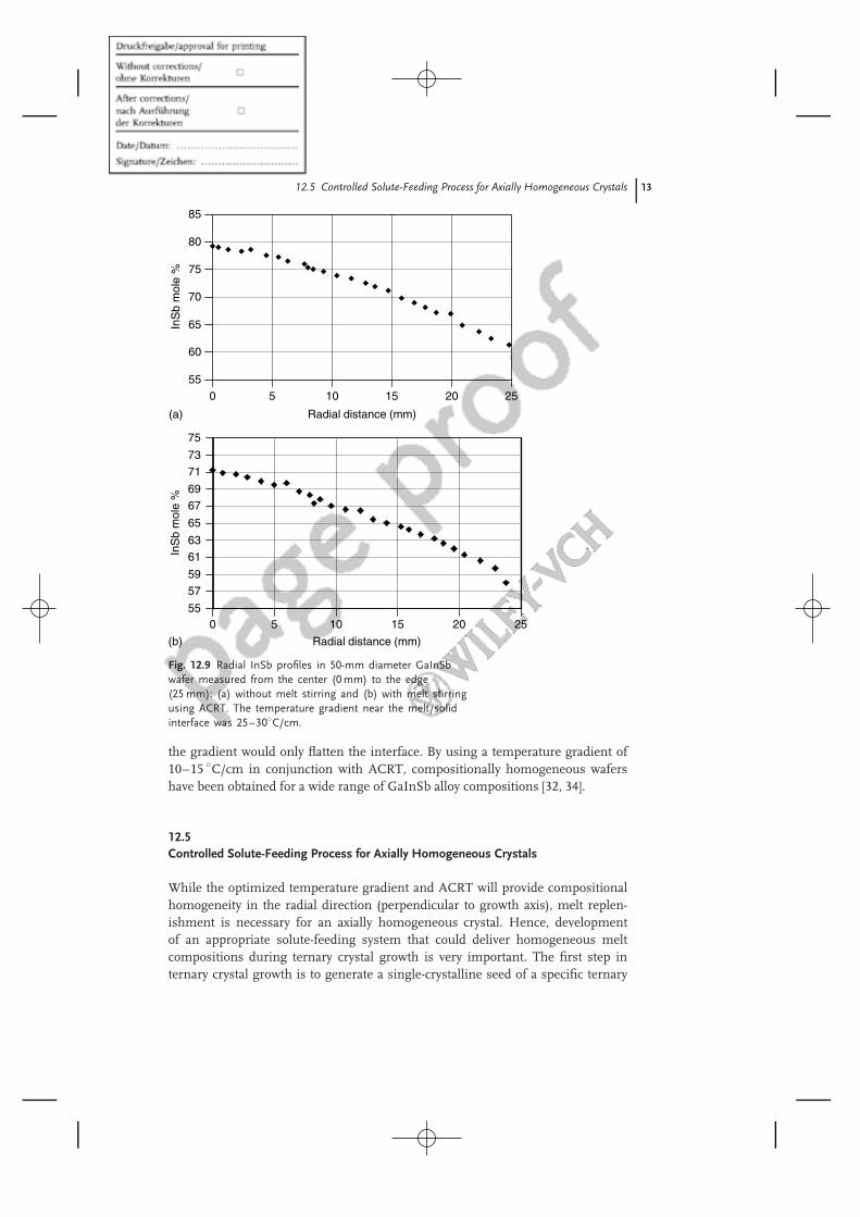
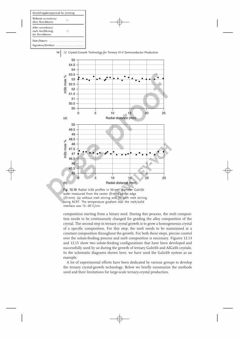
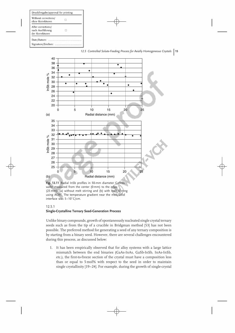
The shape of the melt/solid interface determines the radial compositional profilein ternary crystals [32, 34]. A planar interface is absolutely necessary for obtainingwafers with uniform alloy composition. Hence, it is very important to understandthe heat-transfer processes during ternary crystal growth and identify suitableconditions that could lead to a planar interface during growth. During Bridgmangrowth of ternary crystals, the temperature gradient in the melt, at the melt/solidinterface and in the crystal plays a significant role in deciding the curvature ofthe interface. Interestingly, the effect of forced convection on interface curvatureseems to be weaker than the temperature-gradient effect. Figures 12.9–12.11show the radial InSb composition profiles for VGF grown GaInSb crystals withfurnace temperature gradients of 25–30 ◦C/cm, 15–20 ◦C/cm and 5–10 ◦C/cm,respectively. Under an axial temperature gradient around 30 ◦C/cm, the growthinterface is highly concave with respect to the solid (leading to a convex InSb radialprofile). Without forced convection, at low temperature gradient below 10 ◦C/cm,constitutional supercooling is a major problem. Composition fluctuation due to in-terface breakdown (constitutional supercooling) is observed. The gradient between10–15 ◦C/cm seems to be optimum for stable growth of 50 mm diameter GaInSb[32, 34]. The radial profiles for crystals grown using ACRT have also been shown.ACRT certainly helps avoid constitutional supercooling in the case of a low temper-ature gradient. However, the curved compositional profile at high axial gradientsis very difficult to flatten even with ACRT. This clearly demonstrates the stronginfluence of temperature gradient on the interface curvature. Higher temperaturegradients are known to produce concave melt/solid interface shapes. Lowering
12.5 Controlled Solute-Feeding Process for Axially Homogeneous Crystals 13
55
60
65
70
75
80
85
0 5 10 15 20 25
Radial distance (mm)
InS
b m
ole
%
(a)
55
5759
6163
65
6769
7173
75
0 5 10 15 20 25
Radial distance (mm)
InS
b m
ole
%
(b)
Fig. 12.9 Radial InSb profiles in 50-mm diameter GaInSbwafer measured from the center (0 mm) to the edge(25 mm): (a) without melt stirring and (b) with melt stirringusing ACRT. The temperature gradient near the melt/solidinterface was 25–30◦C/cm.
the gradient would only flatten the interface. By using a temperature gradient of10–15 ◦C/cm in conjunction with ACRT, compositionally homogeneous wafershave been obtained for a wide range of GaInSb alloy compositions [32, 34].
12.5Controlled Solute-Feeding Process for Axially Homogeneous Crystals
While the optimized temperature gradient and ACRT will provide compositionalhomogeneity in the radial direction (perpendicular to growth axis), melt replen-ishment is necessary for an axially homogeneous crystal. Hence, developmentof an appropriate solute-feeding system that could deliver homogeneous meltcompositions during ternary crystal growth is very important. The first step internary crystal growth is to generate a single-crystalline seed of a specific ternary
14 12 Crystal-Growth Technology for Ternary III-V Semiconductor Production
50
50.5
51
51.5
52
52.5
53
53.5
54
54.5
55
0 5 10 15 20 25
Radial distance (mm)
InS
b m
ole
%
(a)
45
45.5
46
46.5
47
47.5
48
48.5
49
49.5
50
0 5 10 15 20 25
Radial distance (mm)
InS
b m
ole
%
(b)
Fig. 12.10 Radial InSb profiles in 50-mm diameter GaInSbwafer measured from the center (0 mm) to the edge(25 mm): (a) without melt stirring and (b) with melt stirringusing ACRT. The temperature gradient near the melt/solidinterface was 15–20◦C/cm.
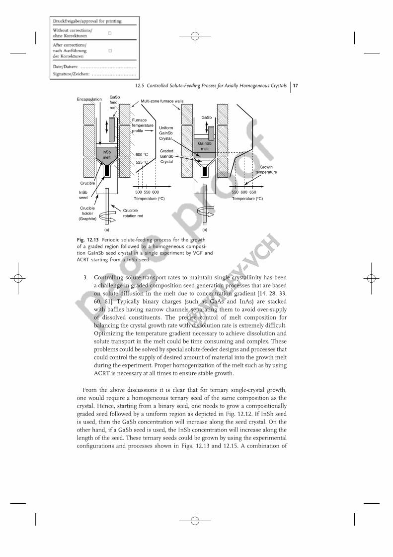
composition starting from a binary seed. During this process, the melt composi-tion needs to be continuously changed for grading the alloy composition of thecrystal. The second step in ternary crystal growth is to grow a homogeneous crystalof a specific composition. For this step, the melt needs to be maintained at aconstant composition throughout the growth. For both these steps, precise controlover the solute-feeding process and melt composition is necessary. Figures 12.13and 12.15 show two solute-feeding configurations that have been developed andsuccessfully used by us during the growth of ternary GaInSb and AlGaSb crystals.In the schematic diagrams shown here, we have used the GaInSb system as anexample.
A lot of experimental efforts have been dedicated by various groups to developthe ternary crystal-growth technology. Below we briefly summarize the methodsused and their limitations for large-scale ternary-crystal production.
12.5 Controlled Solute-Feeding Process for Axially Homogeneous Crystals 15
20
22
24
26
28
30
32
34
36
38
40
0 5 10 15 20 25
Radial distance (mm)
InS
b m
ole
%
(a)
25
2627
28
29
30
3132
3334
35
0 5 10 15 20 25
Radial distance (mm)
InS
b m
ole
%
(b)
Fig. 12.11 Radial InSb profiles in 50-mm diameter GaInSbwafer measured from the center (0 mm) to the edge(25 mm): (a) without melt stirring and (b) with melt stirringusing ACRT. The temperature gradient near the melt/solidinterface was 5–10◦C/cm.
12.5.1Single-Crystalline Ternary Seed-Generation Process
Unlike binary compounds, growth of spontaneously nucleated single crystal ternaryseeds such as from the tip of a crucible in Bridgman method [53] has not beenpossible. The preferred method for generating a seed of any ternary composition isby starting from a binary seed. However, there are several challenges encounteredduring this process, as discussed below:
1. It has been empirically observed that for alloy systems with a large latticemismatch between the end binaries (GaAs-InAs, GaSb-InSb, InAs-InSb,etc.), the first-to-freeze section of the crystal must have a composition lessthan or equal to 5 mol% with respect to the seed in order to maintainsingle crystallinity [19–24]. For example, during the growth of single-crystal
16 12 Crystal-Growth Technology for Ternary III-V Semiconductor Production
GaS
b or
InS
b co
mpo
sitio
n (x
)
0
Crystal length
0.2
0.4
0.6
InSb orGaSb seed
GradedGaInSbRegion
0.8
UniformGaInSbRegion
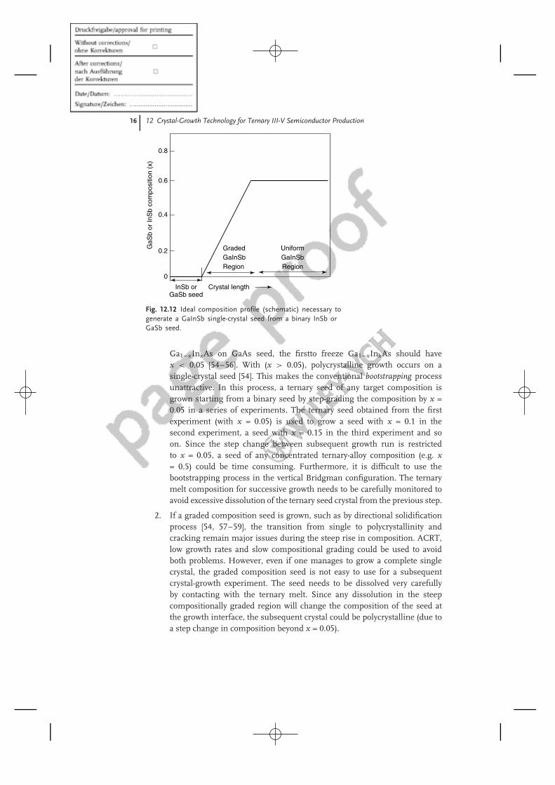
Fig. 12.12 Ideal composition profile (schematic) necessary togenerate a GaInSb single-crystal seed from a binary InSb orGaSb seed.
Ga1−xInxAs on GaAs seed, the firstto freeze Ga1−xInxAs should havex < 0.05 [54–56]. With (x > 0.05), polycrystalline growth occurs on asingle-crystal seed [54]. This makes the conventional bootstrapping processunattractive. In this process, a ternary seed of any target composition isgrown starting from a binary seed by step-grading the composition by x =0.05 in a series of experiments. The ternary seed obtained from the firstexperiment (with x = 0.05) is used to grow a seed with x = 0.1 in thesecond experiment, a seed with x = 0.15 in the third experiment and soon. Since the step change between subsequent growth run is restrictedto x = 0.05, a seed of any concentrated ternary-alloy composition (e.g. x= 0.5) could be time consuming. Furthermore, it is difficult to use thebootstrapping process in the vertical Bridgman configuration. The ternarymelt composition for successive growth needs to be carefully monitored toavoid excessive dissolution of the ternary seed crystal from the previous step.
2. If a graded composition seed is grown, such as by directional solidificationprocess [54, 57–59], the transition from single to polycrystallinity andcracking remain major issues during the steep rise in composition. ACRT,low growth rates and slow compositional grading could be used to avoidboth problems. However, even if one manages to grow a complete singlecrystal, the graded composition seed is not easy to use for a subsequentcrystal-growth experiment. The seed needs to be dissolved very carefullyby contacting with the ternary melt. Since any dissolution in the steepcompositionally graded region will change the composition of the seed atthe growth interface, the subsequent crystal could be polycrystalline (due toa step change in composition beyond x = 0.05).
12.5 Controlled Solute-Feeding Process for Axially Homogeneous Crystals 17
550 600 650
Growthtemperature
Crucibleholder
(Graphite)
InSbseed
GradedGaInSbCrystal
500 550 600
Temperature (°C) Temperature (°C)
Furnacetemperatureprofile
Multi-zone furnace wallsEncapsulation
InSbmelt
(a) (b)
Crucible
GaSbfeedrod
GaInSbmelt
GaSb
UniformGaInSbCrystal
600 °C
525 °C
Cruciblerotation rod
Fig. 12.13 Periodic solute-feeding process for the growthof a graded region followed by a homogeneous composi-tion GaInSb seed crystal in a single experiment by VGF andACRT starting from a InSb seed.
3. Controlling solute-transport rates to maintain single crystallinity has beena challenge in graded-composition seed-generation processes that are basedon solute diffusion in the melt due to concentration gradient [14, 28, 33,60, 61]. Typically binary charges (such as GaAs and InAs) are stackedwith baffles having narrow channels separating them to avoid over-supplyof dissolved constituents. The precise control of melt composition forbalancing the crystal growth rate with dissolution rate is extremely difficult.Optimizing the temperature gradient necessary to achieve dissolution andsolute transport in the melt could be time consuming and complex. Theseproblems could be solved by special solute-feeder designs and processes thatcould control the supply of desired amount of material into the growth meltduring the experiment. Proper homogenization of the melt such as by usingACRT is necessary at all times to ensure stable growth.
From the above discussions it is clear that for ternary single-crystal growth,one would require a homogeneous ternary seed of the same composition as thecrystal. Hence, starting from a binary seed, one needs to grow a compositionallygraded seed followed by a uniform region as depicted in Fig. 12.12. If InSb seedis used, then the GaSb concentration will increase along the seed crystal. On theother hand, if a GaSb seed is used, the InSb concentration will increase along thelength of the seed. These ternary seeds could be grown by using the experimentalconfigurations and processes shown in Figs. 12.13 and 12.15. A combination of
18 12 Crystal-Growth Technology for Ternary III-V Semiconductor Production
0
5
10
15
20
25
30
35
0 5 10 15 20 25 30 35 40 45
Axial distance (mm)
GaS
b m
ole
%
InSb seed
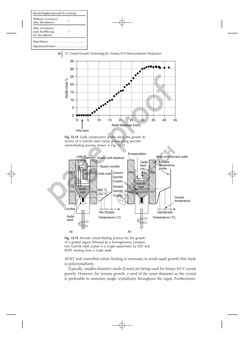
Fig. 12.14 GaSb composition profile along the growth di-rection of a GaInSb seed crystal grown using periodicsolute-feeding process shown in Fig. 12.13.
Encapsulation
550 600 650
Growthtemperature
GaSbseed
Graded
GaInSb
Crystal
700 750 800
Temperature (°C) Temperature (°C)
Furnacetemperatureprofile
Multi-zone furnace walls
GaSbmelt
(a) (b)
Crucible
GaInSbmelt
GaSbfeedrod
Uniform
GaInSb
Crystal
800 °C
725 °C
Quartz melt displacer
InSb melt
InSbdrops
Quartz crucible
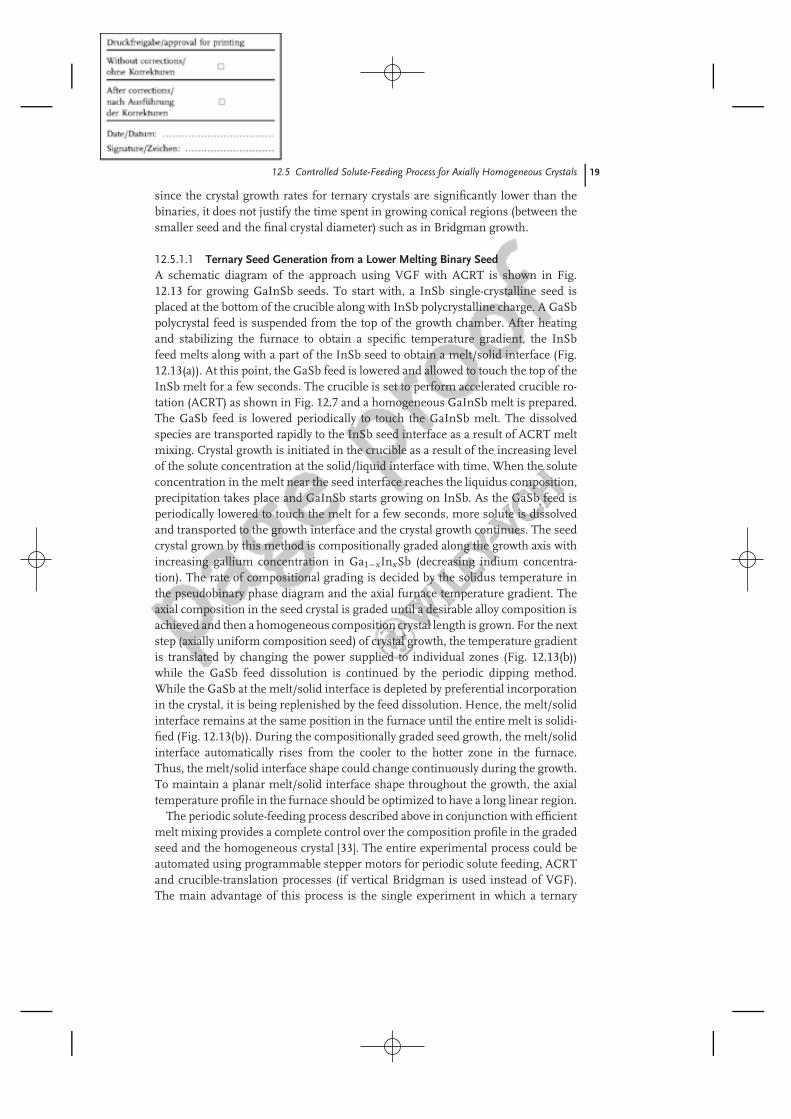
Fig. 12.15 Periodic solute-feeding process for the growthof a graded region followed by a homogeneous composi-tion GaInSb seed crystal in a single experiment by VGF andACRT starting from a GaSb seed.
ACRT and controlled solute feeding is necessary to avoid rapid growth that leadsto polycrystallinity.
Typically, smaller-diameter seeds (5 mm) are being used for binary III-V crystalgrowth. However, for ternary growth, a seed of the same diameter as the crystalis preferable to maintain single crystallinity throughout the ingot. Furthermore,
12.5 Controlled Solute-Feeding Process for Axially Homogeneous Crystals 19
since the crystal growth rates for ternary crystals are significantly lower than thebinaries, it does not justify the time spent in growing conical regions (between thesmaller seed and the final crystal diameter) such as in Bridgman growth.
12.5.1.1 Ternary Seed Generation from a Lower Melting Binary SeedA schematic diagram of the approach using VGF with ACRT is shown in Fig.12.13 for growing GaInSb seeds. To start with, a InSb single-crystalline seed isplaced at the bottom of the crucible along with InSb polycrystalline charge. A GaSbpolycrystal feed is suspended from the top of the growth chamber. After heatingand stabilizing the furnace to obtain a specific temperature gradient, the InSbfeed melts along with a part of the InSb seed to obtain a melt/solid interface (Fig.12.13(a)). At this point, the GaSb feed is lowered and allowed to touch the top of theInSb melt for a few seconds. The crucible is set to perform accelerated crucible ro-tation (ACRT) as shown in Fig. 12.7 and a homogeneous GaInSb melt is prepared.The GaSb feed is lowered periodically to touch the GaInSb melt. The dissolvedspecies are transported rapidly to the InSb seed interface as a result of ACRT meltmixing. Crystal growth is initiated in the crucible as a result of the increasing levelof the solute concentration at the solid/liquid interface with time. When the soluteconcentration in the melt near the seed interface reaches the liquidus composition,precipitation takes place and GaInSb starts growing on InSb. As the GaSb feed isperiodically lowered to touch the melt for a few seconds, more solute is dissolvedand transported to the growth interface and the crystal growth continues. The seedcrystal grown by this method is compositionally graded along the growth axis withincreasing gallium concentration in Ga1−xInxSb (decreasing indium concentra-tion). The rate of compositional grading is decided by the solidus temperature inthe pseudobinary phase diagram and the axial furnace temperature gradient. Theaxial composition in the seed crystal is graded until a desirable alloy composition isachieved and then a homogeneous composition crystal length is grown. For the nextstep (axially uniform composition seed) of crystal growth, the temperature gradientis translated by changing the power supplied to individual zones (Fig. 12.13(b))while the GaSb feed dissolution is continued by the periodic dipping method.While the GaSb at the melt/solid interface is depleted by preferential incorporationin the crystal, it is being replenished by the feed dissolution. Hence, the melt/solidinterface remains at the same position in the furnace until the entire melt is solidi-fied (Fig. 12.13(b)). During the compositionally graded seed growth, the melt/solidinterface automatically rises from the cooler to the hotter zone in the furnace.Thus, the melt/solid interface shape could change continuously during the growth.To maintain a planar melt/solid interface shape throughout the growth, the axialtemperature profile in the furnace should be optimized to have a long linear region.
The periodic solute-feeding process described above in conjunction with efficientmelt mixing provides a complete control over the composition profile in the gradedseed and the homogeneous crystal [33]. The entire experimental process could beautomated using programmable stepper motors for periodic solute feeding, ACRTand crucible-translation processes (if vertical Bridgman is used instead of VGF).The main advantage of this process is the single experiment in which a ternary
20 12 Crystal-Growth Technology for Ternary III-V Semiconductor Production
homogeneous seed crystal of any alloy composition can be obtained starting froma binary single-crystal seed and polycrystalline binary feed materials. For ensuringthe success of this process, the periodic solute-feeding process parameters need tobe fine tuned. This is necessary to precisely control the rate at which solute depletesand replenishes in the melt. The major process parameters that affect the crystallinequality of the seed include solute dipping time and dipping frequency. Dipping timedenotes the actual time the melt is in contact with the feed. This determines theamount of feed introduced in the melt over one period of the dipping cycle. Due tothe temperature gradient in the melt, the top of the melt (higher temperature zone)is usually under-saturated. Hence, the danger of uncontrolled dissolution exists ifthe solute feeding rod is dipped for more than the required time. Thus, a precisecontrol of the dipping time is required. Excess dissolution of the solute can promoterandom nucleation in the entire melt volume. Additionally, this can lead to anoversupply of the solute to the growth interface leading to small grains or causing achange in grain structure. The dipping frequency defines the period of the dippingcycle and should depend on the growth rate. It takes a finite time for the soluteto thoroughly mix with the growth melt. Further, the growth kinetics determinesthe actual growth rate. Based on experimental crystal-growth results [33], a set ofoptimized periodic solute-feeding parameters for GaInSb growth include: solutecontact area of 20 mm, solute dipping time of 2–3 s, solute dipping frequency of3–4 times per hour, temperature gradient near the melt/solid interface of 15 ◦C/cmand ACRT melt mixing process. Figure 12.14 shows the GaSb mole% along thelength of the seed crystal starting from InSb using the process described above.The superior control of the composition profile shown in this diagram clearlydemonstrates the effectiveness of the periodic solute-feeding process.
12.5.1.2 Ternary Seed Generation from a Higher-Melting Binary SeedAnother method for single-crystal seed generation using VGF and ACRT is shownin Fig. 12.15. In this process, the higher melting binary is used as the starting seedmaterial for the ternary seed crystal growth. The process for GaInSb seed genera-tion starting from a GaSb seed has been demonstrated. The experiment starts witha GaSb single-crystalline seed and a GaSb melt in the crucible. The lower meltingpoint binary (InSb in this case) is present in a quartz melt displacer. After the furnacehas been heated, the GaSb feed melts to form a melt/solid interface. The crucible isset to accelerated crucible rotation (ACRT) as in the previous case. By pressing thepiston, the InSb can be periodically fed to the GaSb melt. By controlling the lower-ing rate of the piston, the concentration of InSb in the growth melt can be increasedin a controlled fashion. After the initial InSb melt dispenses into the growth meltto form GaInSb liquid, the temperature of the furnace is slowly lowered to translatethe gradient along the melt like in a VGF process. The graded-composition GaInSbternary starts from the GaSb seed with increasing InSb content in the crystal. TheInSb concentration in the melt increases with time as it is fed into the melt periodi-cally. After the graded GaInSb seed growth, a GaSb feed is introduced into the meltperiodically like in the previous case. The gradient freezing is continued while the
12.6 Steps in Ternary Crystal Production 21
Growthdirection
Fig. 12.16 Cross section of a GaInSb polycrystal seed grownusing the method shown in Fig. 12.15. The GaInSb com-position was graded from a tip-nucleated GaSb seed to ahomogeneous region.
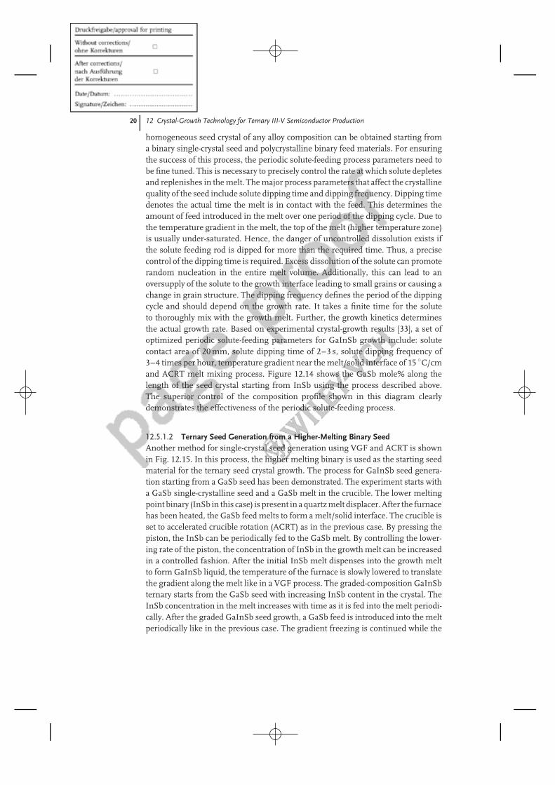
GaSb feed is periodically fed into the melt (Fig. 12.15(b)). This step results in com-positionally uniform GaInSb region. The processes described in Fig. 12.15 can alsobe implemented by the vertical Bridgman method as long as care is taken to ensurethat the GaSb feed shown in Fig. 12.15(b) is introduced into the lower-temperaturezone of the furnace without melting. Figure 12.16 shows the cross section of alarge-grain GaInSb polycrystal seed grown by the method described above startingfrom a tip-nucleated GaSb seed. No cracks could be seen in the entire crystal, demon-strating the success of the solute-feeding process. Figure 12.17 shows the axial InSbmole% in a GaInSb seed grown by the above method starting from a GaSb seed.
12.6Steps in Ternary Crystal Production
Having grown a ternary single-crystal seed of the desired composition, the next stepis to grow a ternary crystal of homogeneous composition from which a large numberof wafers (of the same composition) could be sliced. There are several experimentalconfigurations that could be used to grow homogeneous ternary crystals [62–76].For ternary crystal growth in bottom-seeded crucibles (as discussed here), thepreparation of the growth melt needs to be carried out in a particular fashion.Ensuring the melt composition to be in equilibrium with the seed composition iscrucial for avoiding excessive seed dissolution. Hence, ternary crystal production isa three-step process. Once a seed of a specific alloy composition exists, only steps 2and 3 are necessary for regular production.
22 12 Crystal-Growth Technology for Ternary III-V Semiconductor Production
0
5
10
15
20
25
30
35
40
45
0 5 10 15 20 25 30 35 40 45
Axial distance (mm)
InS
b m
ole
%
GaSb seed
Fig. 12.17 InSb composition profile along the growth di-rection of a GaInSb seed crystal grown using periodicsolute-feeding process shown in Fig. 12.15.
1. The first step is to grow a single-crystal seed of the same alloy compositionas the homogeneous ternary crystal that needs to be produced for generatinglarge number of wafers. For example, if a homogeneous Ga0.8In0.2Sb crystalneeds to be grown, one needs a single-crystal seed of the same alloycomposition. The single-crystal seed must have the same diameter as thediameter of the crystal to be grown. The seed-generation processes werediscussed in Sections 12.5.1.1 and 12.5.1.2. The homogeneous section ofthe seed should be sufficiently long (at least 2–3 cm) such that typical seedremelting (to expose a clean interface) could be carried out before growth.
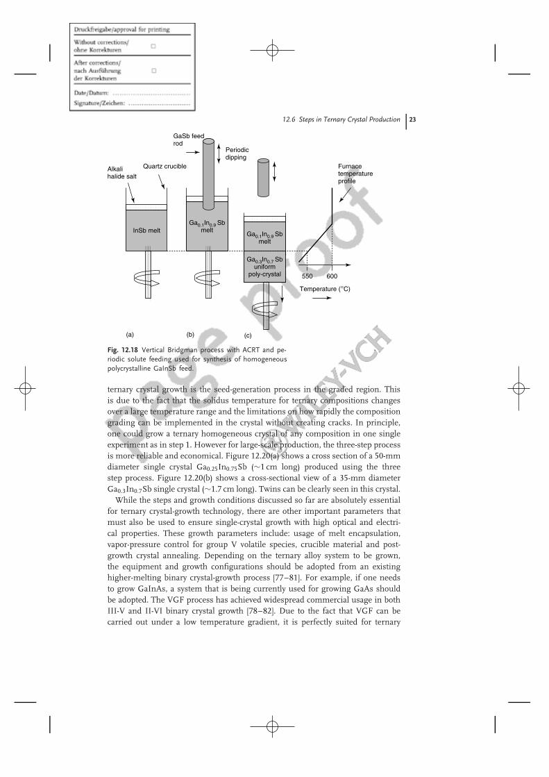
2. The second step is to grow a homogeneous polycrystalline ternary feed ma-terial that could be remelted in the third step discussed below. According tothe GaSb-InSb pseudobinary phase diagram, to grow a Ga0.8In0.2Sb crystal,one would require a melt composition of Ga0.3In0.7Sb with a growth temper-ature of 600 ◦C. Hence one needs to prepare a homogeneous polycrystallineingot of Ga0.3In0.7Sb. For synthesizing the homogeneous polycrystallineingot of Ga0.3In0.7Sb, one could simply use the process shown in Fig. 12.18.Initially, a flat-bottom crucible containing appropriate quantities of GaSband InSb polycrystals is heated to 550 ◦C to obtain a melt of Ga0.1In0.9Sb(liquidus composition corresponding to Ga0.3In0.7Sb solid). The melt is thendirectionally solidified while periodically dissolving GaSb.
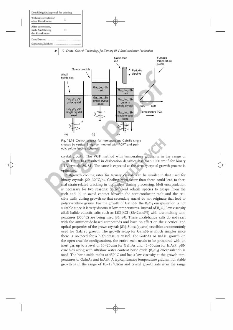
3. In the third and final step, the ternary seed crystal is stacked with the ternarypolycrystalline feed crystal as shown in Fig. 12.19. The polycrystalline feedis carefully melted and a seeding interface is obtained. The melt is thendirectionally solidified while periodically replenishing by dissolving the GaSbfeed rod. This results in a homogeneous ternary single crystal.
In both steps 2 and 3, ACRT is used along with the growth conditions discussedearlier for stable growth. The need for a three-step process discussed above is tosave the overall crystal production time. The most time-consuming process during
12.6 Steps in Ternary Crystal Production 23
GaSb feedrod
InSb meltGa0.1In0.9 Sb
melt
Alkalihalide salt
Quartz crucible
(a) (b) (c)
Ga0.3In0.7 Sbuniform
poly-crystal
Ga0.1In0.9 Sbmelt
550 600
Temperature (°C)
Furnacetemperatureprofile
Periodicdipping
Fig. 12.18 Vertical Bridgman process with ACRT and pe-riodic solute feeding used for synthesis of homogeneouspolycrystalline GaInSb feed.
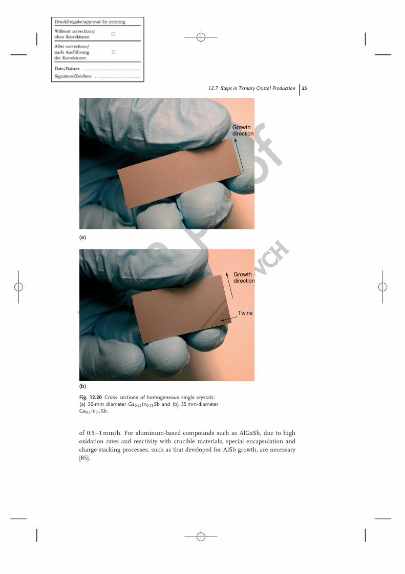
ternary crystal growth is the seed-generation process in the graded region. Thisis due to the fact that the solidus temperature for ternary compositions changesover a large temperature range and the limitations on how rapidly the compositiongrading can be implemented in the crystal without creating cracks. In principle,one could grow a ternary homogeneous crystal of any composition in one singleexperiment as in step 1. However for large-scale production, the three-step processis more reliable and economical. Figure 12.20(a) shows a cross section of a 50-mmdiameter single crystal Ga0.25In0.75Sb (∼1 cm long) produced using the threestep process. Figure 12.20(b) shows a cross-sectional view of a 35-mm diameterGa0.3In0.7Sb single crystal (∼1.7 cm long). Twins can be clearly seen in this crystal.
While the steps and growth conditions discussed so far are absolutely essentialfor ternary crystal-growth technology, there are other important parameters thatmust also be used to ensure single-crystal growth with high optical and electri-cal properties. These growth parameters include: usage of melt encapsulation,vapor-pressure control for group V volatile species, crucible material and post-growth crystal annealing. Depending on the ternary alloy system to be grown,the equipment and growth configurations should be adopted from an existinghigher-melting binary crystal-growth process [77–81]. For example, if one needsto grow GaInAs, a system that is being currently used for growing GaAs shouldbe adopted. The VGF process has achieved widespread commercial usage in bothIII-V and II-VI binary crystal growth [78–82]. Due to the fact that VGF can becarried out under a low temperature gradient, it is perfectly suited for ternary
24 12 Crystal-Growth Technology for Ternary III-V Semiconductor Production
GaSb feedrod
Ga0.3In0.7Sbmelt
Alkalihalide salt
Quartz crucible
(a) (b)
Ga0.8In0.2Sbsingle crystal
seed
Ga0.3In0.7Sbmelt
(c)
600 650
Temperature (°C)
Furnacetemperatureprofile
Periodicdipping
Ga0.8In0.2Sbsingle crystal
seed
Ga0.8In0.2Sbsingle crystal
seed
Ga0.3In0.7Sbpoly-crystal
Ga0.8In0.2Sbuniform
single crystal
Fig. 12.19 Growth process for homogeneous GaInSb singlecrystals by vertical Bridgman method with ACRT and peri-odic solute-feeding schemes.
crystal growth. The VGF method with temperature gradients in the range of1–10 ◦C/cm has resulted in dislocation densities less than 1000 cm−2 for binaryIII-V crystals [80, 81]. The same is expected as the ternary crystal-growth process isoptimized.
Postgrowth cooling rates for ternary crystals can be similar to that used forbinary crystals (20–30 ◦C/h). Cooling rates faster than these could lead to ther-mal strain-related cracking in the wafers during processing. Melt encapsulationis necessary for two reasons: (a) to avoid volatile species to escape from themelt and (b) to avoid contact between the semiconductor melt and the cru-cible walls during growth so that secondary nuclei do not originate that lead topolycrystalline grains. For the growth of GaInSb, the B2O3 encapsulation is notsuitable since it is very viscous at low temperatures. Instead of B2O3, low viscosityalkali-halide eutectic salts such as LiCl-KCl (58:42 mol%) with low melting tem-peratures (350 ◦C) are being used [83, 84]. These alkali-halide salts do not reactwith the antimonide-based compounds and have no effect on the electrical andoptical properties of the grown crystals [83]. Silica (quartz) crucibles are commonlyused for GaInSb growth. The growth setup for GaInSb is much simpler sincethere is no need for a high-pressure vessel. For GaInAs or InAsP growth (inthe open-crucible configuration), the entire melt needs to be pressured with aninert gas up to a level of 10–20 atm for GaInAs and 45–50 atm for InAsP. pBNcrucibles along with ultralow water content boric oxide (B2O3) encapsulation isused. The boric oxide melts at 450 ◦C and has a low viscosity at the growth tem-peratures of GaInAs and InAsP. A typical furnace temperature gradient for stablegrowth is in the range of 10–15 ◦C/cm and crystal growth rate is in the range
12.7 Steps in Ternary Crystal Production 25
Growthdirection
(a)
Growthdirection
Twins
(b)
Fig. 12.20 Cross sections of homogeneous single crystals:(a) 50-mm diameter Ga0.25In0.75Sb and (b) 35 mm-diameterGa0.3In0.7Sb.
of 0.5–1 mm/h. For aluminum-based compounds such as AlGaSb, due to highoxidation rates and reactivity with crucible materials, special encapsulation andcharge-stacking processes, such as that developed for AlSb growth, are necessary[85].
26 12 Crystal-Growth Technology for Ternary III-V Semiconductor Production
12.7Current Status of Ternary Substrates
Most of the ternary III-V crystal production efforts are focused towards large-grainpolycrystalline growth for applications such as thermophotovoltaics, infrared opticalcomponents, homojunction optoelectronic devices such as photodetectors andterahertz emitters, etc. [11, 12, 33, 38–44, 86]. The optical and electrical propertiesof these crystals are close to their highest theoretical limits and are perfectlysuited for the above applications. Evaluation of single-crystalline material forheteroepitaxial device fabrication has not yet been initiated. This is due to lackof a steady supply of epiready ternary wafers from any high-profile commercialvendors. Data on crystalline quality such as spatial dislocation density profile,microscopic alloy fluctuation, thermal properties, etc., is still lacking. Limitedmeasurements on GaInSb single crystals grown using vertical Bridgman andVGF methods have revealed dislocation densities of 1000–2000 cm−2, which isvery encouraging. Proving high crystalline quality using X-ray rocking curves,availability of misoriented substrates and demonstration of high surface qualityare absolutely necessary for widespread usage in electronic and optoelectronicapplications where lattice-matched substrates are needed.
12.8Conclusion
Substrates of III-V ternary compounds with variable properties have potentialfor many large-scale emerging photonic, electronic and photovoltaic applications.The materials-science issues and crystal-growth challenges have already beenunderstood and established. This chapter presented a comprehensive treatmentof various problems encountered during bulk ternary crystal growth from themelt and methods to solve them. The only barrier to large-scale ternary crystalproduction is the development of an appropriate engineering infrastructure. Thiscould be accomplished by starting from existing binary crystal-growth systems.From extensive work, it has been concluded that the vertical Bridgman or verticalgradient freezing process is the most suitable method for growing large-diameterIII-V ternary bulk crystals. In this chapter, a crystal-growth process designedfor large-diameter ternary crystals has been described. The established processhas been successfully demonstrated in laboratory-scale experiments for growingGaInSb crystals (up to 50 mm diameter) with a wide range of alloy compositions.Limited experiments on AlGaSb, GaInAs and InAsP have also been carried outto evaluate the growth parameters necessary to grow crystals with high opticaland electrical properties. Crucial growth parameters include: low temperaturegradient, low growth rate compared to binary compounds and melt stirring usingforced convection to avoid constitutional supercooling. For generating ternarysingle-crystal seeds, a two-step process is necessary. Growth of homogeneoussingle crystals requires precise melt composition control using periodic solutereplenishment and continuous melt stirring such as with ACRT.
References 27
References
1. V. Swaminathan, A. T. Macrander, 1991,Materials Aspects of GaAs and InP BasedStructures, Prentice-Hall, Inc., New Jer-sey.
2. R. Koyama, 1995, Gallium ArsenideMicroelectronic Devices and Circuits,in Handbook of Compound Semicon-ductors – Growth, Processing, Char-acterization, Devices, William An-drew Publishing/Noyes p. 772.
3. D. Lile, 1995, Optoelectronic Devices,in Handbook of Compound Semicon-ductors – Growth, Processing, Char-acterization, Devices, William An-drew Publishing/Noyes, p. 814.
4. P. S. Dutta, H. L. Bhat, V. Kumar,1997, J. Appl. Phys. 81, 5821.
5. I. Vurgaftman, J. R. Meyer, L. R.Ram-Mohan, 2001, J. Appl. Phys. 89(11),5815.
6. Special issue on Compliant, alternativesubstrate technology, J. Electron. Mater.29, 2000.
7. K. Otsubo, H. Shoji, T. Kusunoki, T.Suziki, T. Uchida, Y. Nishijina, H.Ishikawa, 1997, Electron Lett. 33, 1795.
8. H. Ishikawa, 1993, Appl. Phys. Lett. 63,712.
9. K. Otsubo, Y. Nishijima, T. Uchida,H. Shoji, K. Nakajima, H. Ishikawa,1999, Jpn. J. Appl. Phys. 38, L312.
10. H.X. Yuan, D. Grubisic, T.T.S. Wong,1999, J. Electron. Mater. 28, 39.
11. T. Refaat, M. N. Abedin, V. Bhagwat,I.B. Bhat, P.S. Dutta, U.N. Singh,2004, Appl. Phys. Lett. 85(11), 1874.
12. G. Rajagopalan, N. S. Reddy, H. Ehsani,I. B. Bhat, P. S. Dutta, R. J. Gutmann,G. Nichols, G. W. Charache, O. Sulima,2003, J. Electron. Mater. 32(11), 1317.
13. K.I. Chang, Y.C.M. Yeh, P.A. Iles, J.M.Tracy, R.K. Morris, 1987, 19th IEEE Pho-tovoltaic Specialists Conference Issue 273.
14. K. Nakajima, S. Kodama, S. Miyashita,G. Sazaki, S. Hiyamizu, 1999, J. Cryst.Growth 205, 270.
15. G.W. Charache, D.M. Depoy, P.F.Baldasaro, 1998, Compd. Semicond. 4(7),36.
16. Antimonide-related Strained-layer Het-erostructures (ed.) M.O. Manasreh, 1997,
in: Optoelectronic Properties of Semi-conductors, Superlattices, Vol. 3, Gor-don Breach Science Publishers.
17. K.J. Bachmann, F.A. Thiel, H. SchreiberJr., 1979, Prog. Cryst. Growth Charac. 2,171.
18. K. Nakajima, K. Osamura, K. Yasuda,Y. Murakami, 1977, J. Cryst. Growth 41,87.
19. W.A. Bonner, B.J. Skromme, E. Berry,H.L. Gilchrist, R.E. Nahory, 1989, in:J.S. Harris (ed.), Proc. of the 15th Inter-national Symposium on GaAs and Re-lated Compounds, Atlanta, GA 1988, In-stitute of Physics Conference Series, Vol.96,Institute of Physics, Bristol, p. 337.
20. W.A. Bonner, B. Lent, D.J. Freschi, W.Hoke, 1994, in Producibility of II-VIMaterials, Devices, SPIE, 2228, 33.
21. S. Kodama, Y. Furumura, K. Kinoshita,H. Kato, S. Yoda, 2000, J. Cryst. Growth208, 165.
22. Y. Nishijima, K. Nakajima, K. Otsubo,H. Ishikawa, 2000, J. Cryst. Growth 208,171.
23. A. Tanaka, J. Shintani, M. Kimura, T.Sukegawa, 2000, J. Cryst. Growth 209,625.
24. T. Suzuki, K. Nakajima, T. Kusunoki,T. Katoh, 1996, J. Electron. Mater. 25(3),357.
25. P.S. Dutta, A.G. Ostrogorsky, 1998, J.Cryst. Growth 194, 1.
26. P.S. Dutta, A.G. Ostrogorsky, 1999,J. Cryst. Growth 198/199, 384.
27. P.S. Dutta, A.G. Ostrogorsky, 1999, J.Cryst. Growth 197, 1.
28. P.S. Dutta, 2005, J. Cryst. Growth 275,106.
29. P.S. Dutta and T.R. Miller, 2000, J. Elec-tron. Mater. 29, 956.
30. P.S. Dutta, T.R. Miller, 2003, Multicom-ponent homogeneous alloys and methodfor making same, US 6613162 B1.
31. P.S. Dutta, A.G. Ostrogorsky, 2001, Al-loys and methods for their preparation, US6273969 B1.
32. H.J. Kim, 2005, Ph.D. Thesis, RensselaerPolytechnic Institute, Troy, New York,Bulk Crystal-growth process for Composi-tionally Homogeneous GaInSb Substrates.
28 12 Crystal-Growth Technology for Ternary III-V Semiconductor Production
33. A. Chandola, 2005, Ph.D. Thesis, Rens-selaer Polytechnic Institute, Troy, NewYork, Bulk Crystal Growth and In-frared Absorption Studies of GaInSb.
34. H. Kim, A. Chandola, R. Bhat, P.S.Dutta, 2006, J. Cryst. Growth 289, 450.
35. E. Scheil, 1942, Z. Metallkde. 34, 70.36. W. G. Pfann, 1952, J. Met. 4, 747.37. J. A. Burton, R. C. Prim, W. P. Slichter,
1953, J. Chem. Phys. 21, 1987.38. R. Pino, Y. Ko, P.S. Dutta, 2004,
J. Electron. Mater. 33(9), 1012.39. A. Chandola, H.J. Kim, S. Guha,
L. Gonzalez, V. Kumar, P.S. Dutta,2005, J. Appl. Phys. 98, 093103.
40. H. Kim, A. Chandola, S. Guha, L.Gonzalez, V. Kumar, P.S. Dutta, 2005,J. Electron. Mater. 34(11), 1391.
41. A. Chandola, R. Pino, P.S. Dutta, 2005,Semicond. Sci. Technol. 20, 886.
42. R. Pino, Y. Ko, P.S. Dutta, 2004, Int. J.High Speed Electron. Syst. 14(3), 658.
43. R. Pino, Y. Ko, P.S. Dutta, 2004, J. Appl.Phys. 96(2), 1064.
44. R. Pino, Y. Ko, P.S. Dutta, S. Guha,L.P. Gonzalez, 2004, J. Appl. Phys. 96(9),5349.
45. J. B. Mullin, 1999, An historical per-spective, in: K.W. Benz (ed.), The Roleof Magnetic Fields in Crystal Growth,Prog. Crystal Growth Charact. Mater. 38.
46. D. Elwell, H. J. Scheel, 1975, Crys-tal Growth from High-Temperature So-lutions, Academic Press, London.
47. H. J. Scheel, R. H. Swendsen, 2001, J.Cryst. Growth 233, 609.
48. H. J. Scheel, E. O. Schulz-Dubois,1971, J. Cryst. Growth 8, 304.
49. H. J. Scheel, 1972, J. Cryst. Growth 13/14,560.
50. P. Capper, 2005, Bulk Growth of Cad-mium Mercury Telluride (CMT), inBulk Crystal Growth of Electronic,Optical, Optoelectronic Materials,(ed.), P. Capper, John Wiley, Sons,Ltd., Chichester, UK, Chap. 7.
51. K. Juliet Vogel, 2004, Ph.D Thesis, Rens-selaer Polytechnic Institute, Troy, NewYork, Solute Redistribution and Consti-tutional Supercooling Effects in Verti-cal Bridgman Grown InGaSb by Accel-erated Crucible Rotation Technique.
52. W. A. Tiller, K. A. Jackson, J. W. Rutter,B. Chalmers, 1953, Acta Met. 1, 428.
53. W.D. Lawson, S. Nielsen, 1958, Prepa-ration of Single Crystals, ButterworthsScientific Publications, London.
54. Y. Nishijima, K. Nakajima, K. Otsubo,H. Ishikawa, 1999, J. Cryst. Growth 197,769.
55. D. Reid, B. Lent, T. Bryskiewicz, P.Singer, E. Mortimer, W. A. Bonner,1997, J. Cryst. Growth 174, 250.
56. W. A. Bonner, R. E. Nahory, H. L.Gilchrist, E. Berry, 1990, Semi-InsulatingIII-V Materials p. 199.
57. K. Nakajima, T. Kusunoki, K. Otsubo,1997, J. Cryst. Growth 173, 42.
58. Y. Nishijima, K. Nakajima, K. Otsubo,H. Ishikawa, 2000, J. Cryst. Growth 208,171.
59. K. Hashio, M. Tatsumi, H. Kato, K.Kinoshita, 2000, J. Cryst. Growth 210,471.
60. W. G. Cochran, 1934, Proc. Camb. Philos.Soc. 30, 365.
61. A. Watanabe, A. Tanaka, T. Sukegawa,1993, Jpn. J. Appl. Phys. 32, 793.
62. H.-J. Sell, 1991, J. Cryst. Growth 107,396.
63. W. F. Leverton, 1958, J. Appl. Phys. 29,1241.
64. T. Kusunoki, K. Nakajima, K. Kuramata,1992, Inst. Phys. Conf. Ser. 129, 37.
65. K. Nakajima, T. Kusunoki, 1991,Inst. Phys. Conf. Ser. 120, 67.
66. T. Kusunoki, C. Takenaka, K. Nakajima,1991, J. Cryst. Growth 115, 723.
67. T. Ashley, J.A. Beswick, B. Cockayne,C.T. Elliott, 1995, Inst. Phys. Conf. Ser.144, 209.
68. A. Tanaka, A. Watanabe, M. Kimura, T.Sukegawa, 1994, J. Cryst. Growth 135,269.
69. A. Tanaka, T. Yoneyama, M. Kimura, T.Sukegawa, 1998, J. Cryst. Growth 186,305.
70. M.H. Lin, S. Kou, 1998, J. Cryst. Growth193, 443.
71. M. H. Lin, S. Kou, 1993, J. Cryst. Growth132, 461.
72. T. Ozawa, Y. Hayakawa, M. Kumagawa,1991/2001, J. Cryst. Growth 109,212; J. Cryst. Growth 229, 124.
73. K. Kinoshita, H. Kato, S. Yado,2000, J. Cryst. Growth 216, 37.
74. K. Kinoshita, H. Kato, S. Matsumoto, S.Yoda, 2001, J. Cryst. Growth 225, 59.
References 29
75. W.F.H. Micklethwaite, 2005, BulkGrowth of InSb and Related Ternary Al-loys, in Bulk Crystal Growth of Elec-tronic, Optical, Optoelectronic Mate-rials, (ed.), P. Capper, John Wiley &Sons, Ltd., Chichester, UK, Chap. 5.
76. P.S. Dutta, 2005, Method and Appa-ratus for Growth of Multi-ComponentSingle Crystals US Patent Pending.
77. R. K. Willardson, H.L. Goering, 1962,Compound Semiconductors, Vol. 1 Prepa-ration of III-V Compounds, ReinholdPublishing Corporation, New York.
78. I.R. Grant, 2005, InP Crystal Growth,in Bulk Crystal Growth of Electronic,Optical, Optoelectronic Materials,(ed.), P. Capper, John Wiley & Sons,Ltd., Chichester, UK, Chap. 4.
79. M.R. Brozel, I.R. Grant, 2005, Growth ofGaAs, in Bulk Crystal Growth of Elec-tronic, Optical, Optoelectronic Mate-rials, (ed.), P. Capper, John Wiley &Sons, Ltd., Chichester, UK, Chap. 2.
80. T. Asahi, K. Kainosho, K. Kohiro, A.Noda, K. Sato, O. Oda, 2003, Growthof III-V and II-VI Single Crystals by
the Vertical Gradient-freeze Method,in Crystal Growth Technology, (eds.)H.J. Scheel, T. Fukuda, John Wiley &Sons, Ltd., Chichester, UK, Chap. 16.
81. T. Kawase, M. Tatsumi, Y. Nishida,2003, Growth Technology of III-V Sin-gle Crystals for Production, in Crys-tal Growth Technology, (eds.) H.J.Scheel, T. Fukuda, John Wiley & Sons,Ltd., Chichester, UK, Chap. 16.
82. W.A. Gault, E.M. Monberg, J.E. Clemens,1986, J. Cryst. Growth 74, 491.
83. T. Duffar, J.M. Gourbil, P. Boiton,P. Dusserre, N. Eustathopoulos,1997, J. Cryst. Growth 179, 356.
84. P.S. Dutta, A.G. Ostrogorsky, R.J.Gutmann, 1997, ‘‘Bulk Growth of GaSband GaxIn1−xSb’’, Third NREL Confer-ence on Thermophotovoltaic Generationof Electricity, Colorado Springs, Col-orado, AIP Conf. Proc. 401, p. 157.
85. R. Pino, Y. Ko, P.S. Dutta, 2006, J. Cryst.Growth 290, 29.
86. R. Ascazubi, I. Wilke, K.J. Kim, P.S.Dutta, 2006, Phys. Rev. B 74, 075323.
keywords/abstract
Dear author,
Please check and/or supply keywords (3 to 5) and an abstract. These will not beincluded in the print version of your chapter but in the online version. If you donot supply an abstract, the section heading will be used instead.
Thank you!
Abstract
Substrates of III-V ternary compound semiconductors with variable bandgaps orlattice constants still remain very attractive for a variety of electronic, optoelec-tronic, and photovoltaic devices. However, the commercial technology for growinglarge-diameter, compositionally homogeneous, bulk III-V ternary crystals has notbeen fully developed. This chapter discusses the fundamental challenges that haveimpeded the rapid progress of ternary crystal growth. Due to the intrinsic separa-tion between liquidus and solidus in the pseudobinary phase diagrams used forgrowing ternary crystals, alloy segregation is a major issue. This, in turn, leadsto (a) low yield of wafers with the same composition, (b) cracking of crystals dueto constitutional supercooling and strain arising from the compositional grading,and (c) nonhomogeneous wafers due to the curved solid/liquid interface shape.Some of the recent advances made to overcome these challenges for the growthof Al-Ga-In-As-P-Sb-based ternary substrates have been presented. The precisecontrol of heat and mass transport in the melt that is necessary during ternarycrystal growth will be discussed. In particular, the crucial role of melt stirring usingaccelerated crucible rotation technique (ACRT) has been highlighted. The verticalBridgman (VB) or vertical gradient freezing (VGF) techniques in conjunction withACRT have been found to be most suitable and successfully employed for growingternary crystals with a wide range of alloy compositions. In this chapter, we willdiscuss various concepts using GaInSb as a model material due to the extensivenature of work that has been carried out on this system. The growth processesdeveloped for GaInSb have been found to translate well to other alloy systems suchas GaInAs, InAsP and AlGaSb with appropriate modifications for vapor-pressurecontrol. The growth results from these crystals will not be presented here sincethey are still in the initial stages of development.
Keywords
Q1

Queries in Chapter 12
Q1. Au: Please provide ‘‘Keywords’’.


![Ternary Logic Gates and Ternary SRAM Cell ….pdf · According to blueprint of Weste & Harris in [4] for design of a binary SRAM, a ternary SRAM is constructed similarly. A ternary](https://img.pdfslide.us/doc/110x75/5a8290bb7f8b9aa24f8e2227/ternary-logic-gates-and-ternary-sram-cell-pdfaccording-to-blueprint-of-weste.jpg)