Embed Size (px)
Citation preview
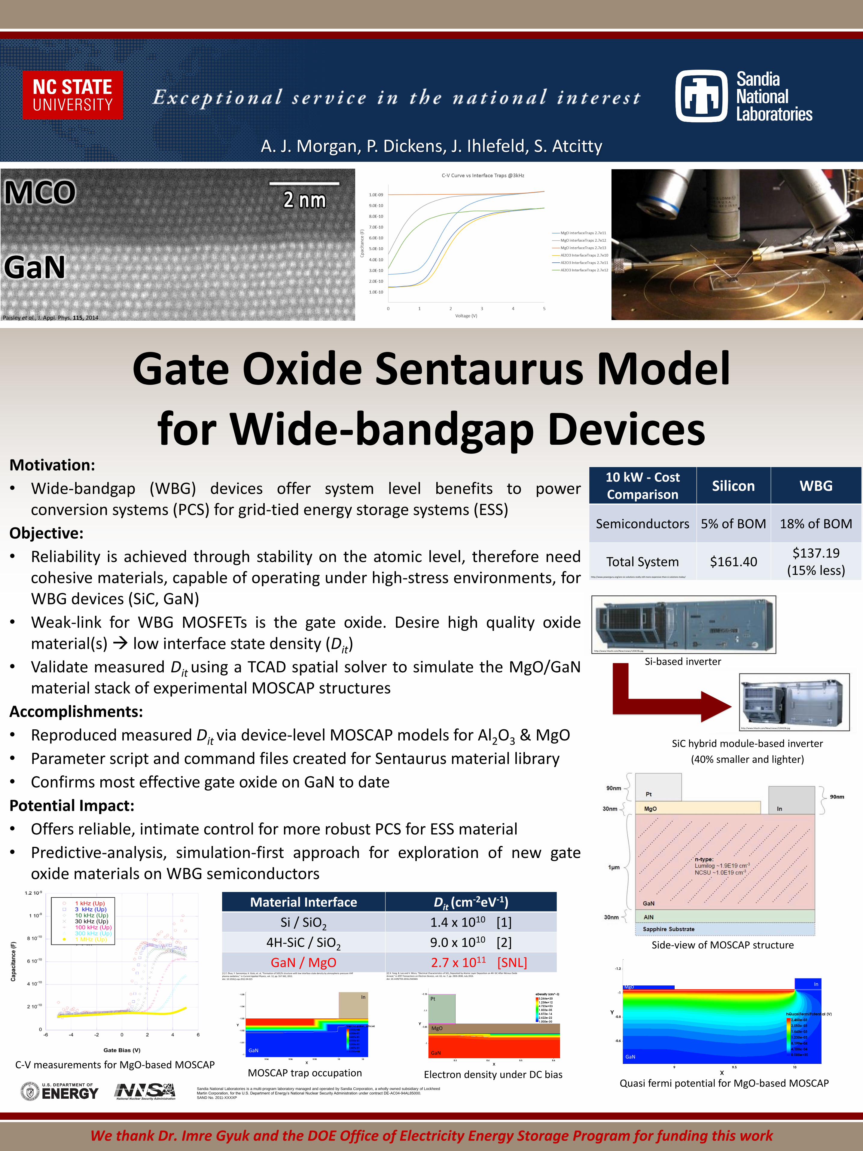
Gate Oxide Sentaurus Model for Wide-bandgap Devices
Sandia National Laboratories is a multi-program laboratory managed and operated by Sandia Corporation, a wholly owned subsidiary of Lockheed
Martin Corporation, for the U.S. Department of Energy’s National Nuclear Security Administration under contract DE-AC04-94AL85000.
SAND No. 2011-XXXXP
GaN
MCO
Paisley et al., J. Appl. Phys. 115, 2014
Motivation:
• Wide-bandgap (WBG) devices offer system level benefits to powerconversion systems (PCS) for grid-tied energy storage systems (ESS)
Objective:
• Reliability is achieved through stability on the atomic level, therefore needcohesive materials, capable of operating under high-stress environments, forWBG devices (SiC, GaN)
• Weak-link for WBG MOSFETs is the gate oxide. Desire high quality oxidematerial(s) low interface state density (Dit)
• Validate measured Dit using a TCAD spatial solver to simulate the MgO/GaNmaterial stack of experimental MOSCAP structures
Accomplishments:
• Reproduced measured Dit via device-level MOSCAP models for Al2O3 & MgO
• Parameter script and command files created for Sentaurus material library
• Confirms most effective gate oxide on GaN to date
Potential Impact:
• Offers reliable, intimate control for more robust PCS for ESS material
• Predictive-analysis, simulation-first approach for exploration of new gateoxide materials on WBG semiconductors
We thank Dr. Imre Gyuk and the DOE Office of Electricity Energy Storage Program for funding this work
A. J. Morgan, P. Dickens, J. Ihlefeld, S. Atcitty
Si-based inverter
SiC hybrid module-based inverter
(40% smaller and lighter)
http://www.hitachi.com/New/cnews/120419b.jpg
http://www.hitachi.com/New/cnews/120419b.jpg
10 kW - CostComparison
Silicon WBG
Semiconductors 5% of BOM 18% of BOM
Total System $161.40$137.19
(15% less)http://www.powerguru.org/are-sic-solutions-really-still-more-expensive-than-si-solutions-today/
Material Interface Dit (cm-2eV-1)
Si / SiO2 1.4 x 10¹⁰ [1]
4H-SiC / SiO2 9.0 x 10¹⁰ [2]
GaN / MgO 2.7 x 10¹¹ [SNL][2] X. Yang, B. Lee and V. Misra, "Electrical Characteristics of SiO2 Deposited by Atomic Layer Deposition on 4H–SiC After Nitrous Oxide Anneal," in IEEE Transactions on Electron Devices, vol. 63, no. 7, pp. 2826-2830, July 2016.doi: 10.1109/TED.2016.2565665
[1] Z. Zhuo, Y. Sannomiya, K. Goto, et. al, “Formation of Si02/Si structure with low interface state density by atmospheric-pressure VHF plasma oxidation," in Current Applied Physics, vol. 12, pp. S57-S62, 2012.doi: 10.1016/j.cap.2012.04.015
Side-view of MOSCAP structure
C-V measurements for MgO-based MOSCAPElectron density under DC bias
Pt
MgO
GaN
MOSCAP trap occupation
GaN
In
Quasi fermi potential for MgO-based MOSCAP
GaN
InMgO