Embed Size (px)
Citation preview
11.1 Band Theory of Solids 11.4 Nanotechnology
CHAPTER 11Semiconductor Theory and DevicesSemiconductor Theory and Devices
Categories of Solids
There are three categories of solids, based on their conducting properties: conductors semiconductors insulators
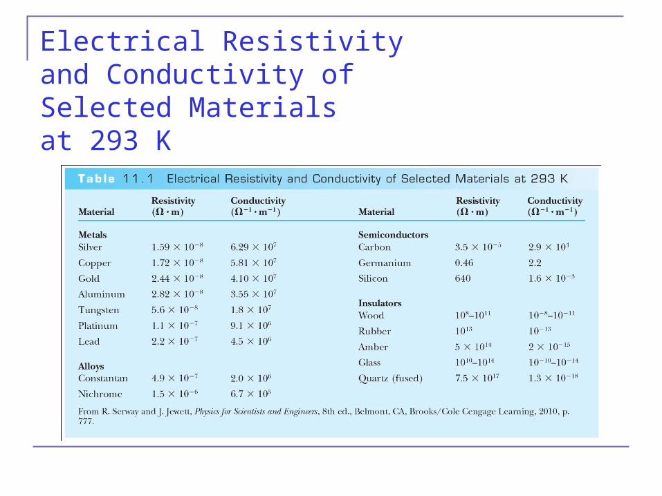
Electrical Resistivity and Conductivity of Selected Materials at 293 K
Reviewing the previous table reveals that:
The electrical conductivity at room temperature is quite different for each of these three kinds of solids Metals and alloys have the highest conductivities followed by semiconductors and then by insulators
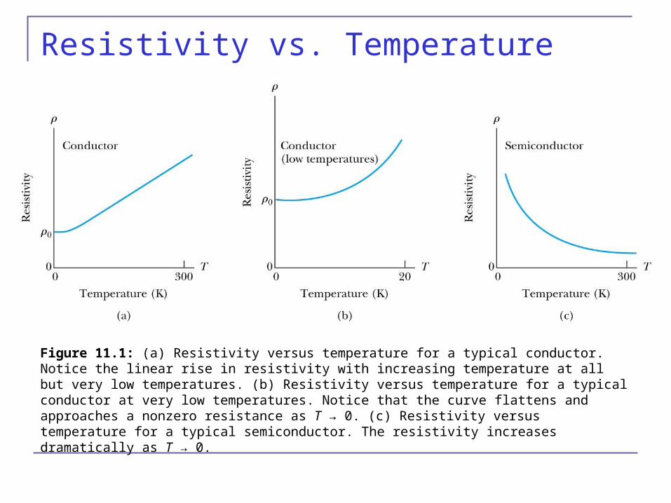
Resistivity vs. Temperature
Figure 11.1: (a) Resistivity versus temperature for a typical conductor. Notice the linear rise in resistivity with increasing temperature at all but very low temperatures. (b) Resistivity versus temperature for a typical conductor at very low temperatures. Notice that the curve flattens and approaches a nonzero resistance as T → 0. (c) Resistivity versus temperature for a typical semiconductor. The resistivity increases dramatically as T → 0.
In order to account for decreasing resistivity with increasing temperature as well as other properties of semiconductors, a new theory known as the band theory is introduced.
The essential feature of the band theory is that the allowed energy states for electrons are nearly continuous over certain ranges, called energy bands, with forbidden energy gaps between the bands.
Band Theory of Solids
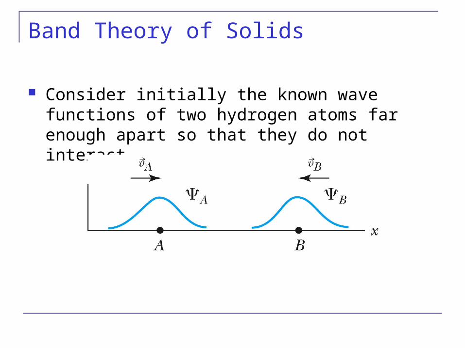
Consider initially the known wave functions of two hydrogen atoms far enough apart so that they do not interact.
Band Theory of Solids
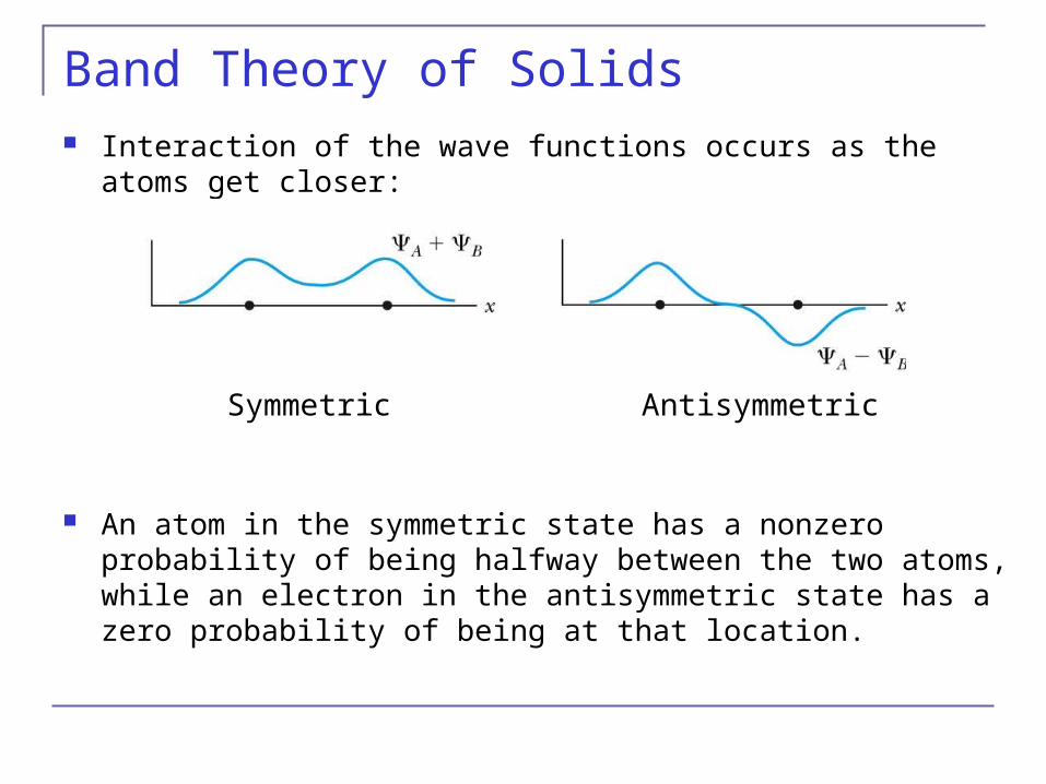
Band Theory of Solids Interaction of the wave functions occurs as the atoms get closer:
An atom in the symmetric state has a nonzero probability of being
halfway between the two atoms, while an electron in the antisymmetric state has a zero probability of being at that location.
Symmetric Antisymmetric
Band Theory of Solids
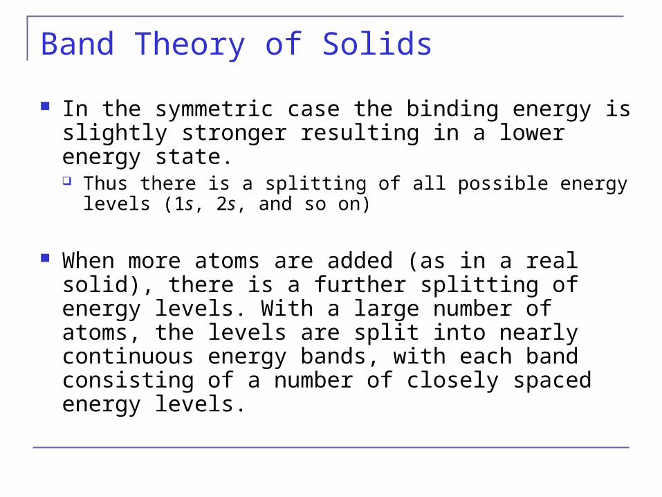
In the symmetric case the binding energy is slightly stronger resulting in a lower energy state. Thus there is a splitting of all possible energy levels (1s,
2s, and so on)
When more atoms are added (as in a real solid), there is a further splitting of energy levels. With a large number of atoms, the levels are split into nearly continuous energy bands, with each band consisting of a number of closely spaced energy levels.
Kronig-Penney Model
An effective way to understand the energy gap in semiconductors is to model the interaction between the electrons and the lattice of atoms.
R. de L. Kronig and W. G. Penney developed a useful one-dimensional model of the electron lattice interaction in 1931.
Kronig-Penney Model
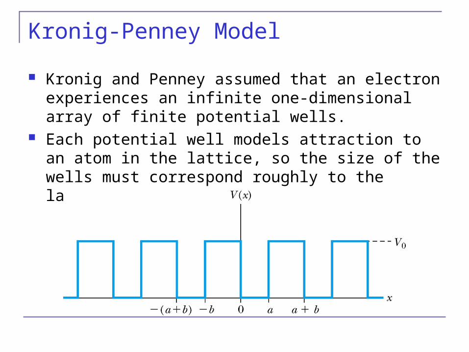
Kronig and Penney assumed that an electron experiences an infinite one-dimensional array of finite potential wells.
Each potential well models attraction to an atom in the lattice, so the size of the wells must correspond roughly to the lattice spacing.
Kronig-Penney Model
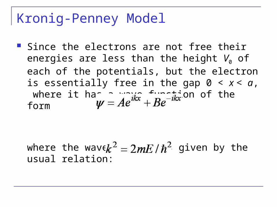
Since the electrons are not free their energies are less than the height V0 of each of the potentials, but the electron is essentially free in the gap 0 < x < a, where it has a wave function of the form
where the wave number k is given by the usual relation:
Tunneling
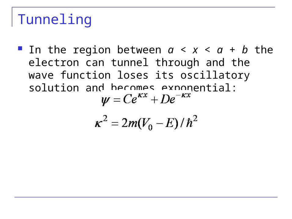
In the region between a < x < a + b the electron can tunnel through and the wave function loses its oscillatory solution and becomes exponential:
Kronig-Penney Model
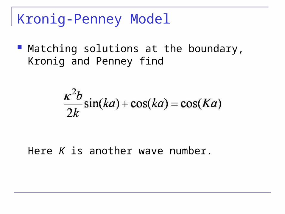
Matching solutions at the boundary, Kronig and Penney find
Here K is another wave number.
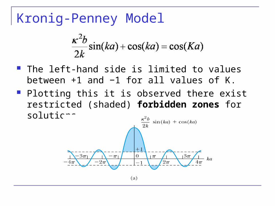
The left-hand side is limited to values between +1 and −1 for all values of K.
Plotting this it is observed there exist restricted (shaded) forbidden zones for solutions.
Kronig-Penney Model
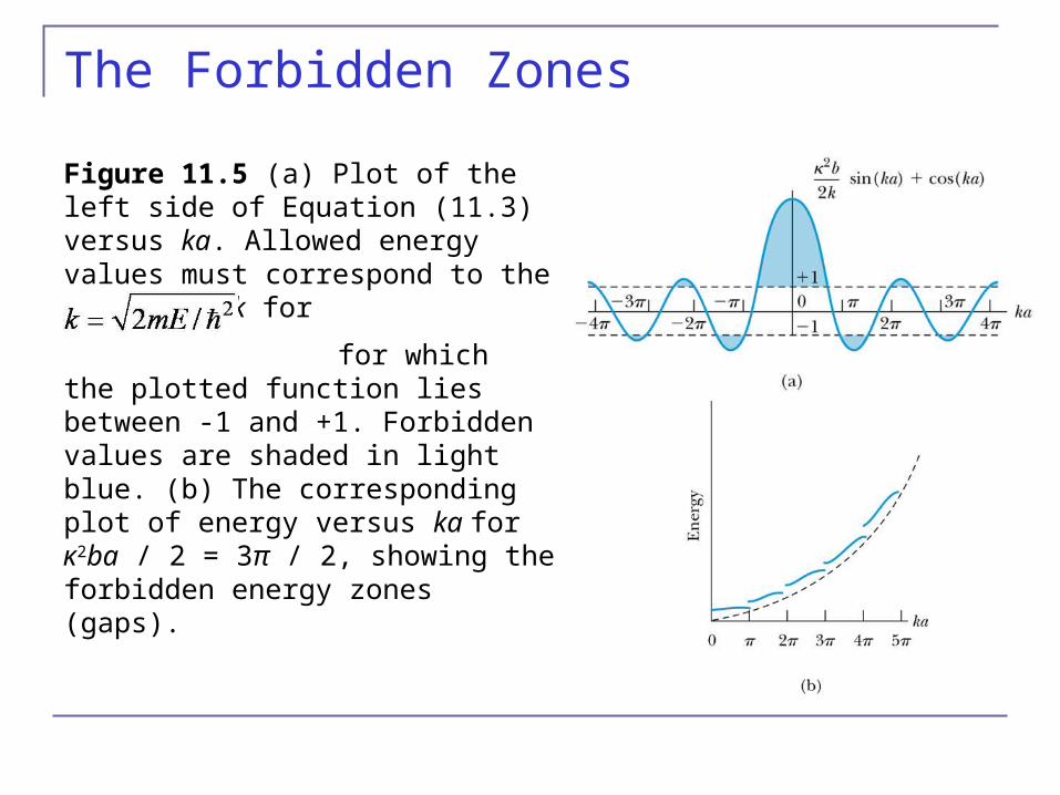
Figure 11.5 (a) Plot of the left side of Equation (11.3) versus ka. Allowed energy values must correspond to the values of k for
for which the plotted function lies between -1 and +1. Forbidden values are shaded in light blue. (b) The corresponding plot of energy versus ka for κ2ba / 2 = 3π / 2, showing the forbidden energy zones (gaps).
The Forbidden Zones
Important differences between the Kronig-Penney model and the single potential well
1) For an infinite lattice the allowed energies within each band are continuous rather than discrete. In a real crystal the lattice is not infinite, but even if chains are thousands of atoms long, the allowed energies are nearly continuous.
2) In a real three-dimensional crystal it is appropriate to speak of a wave vector . The allowed ranges for constitute what are referred to in solid state theory as Brillouin zones.
And…
3) In a real crystal the potential function is more complicated than the Kronig-Penney squares. Thus, the energy gaps are by no means uniform in size. The gap sizes may be changed by the introduction of impurities or imperfections of the lattice.
These facts concerning the energy gaps are of paramount importance in understanding the electronic behavior of semiconductors.
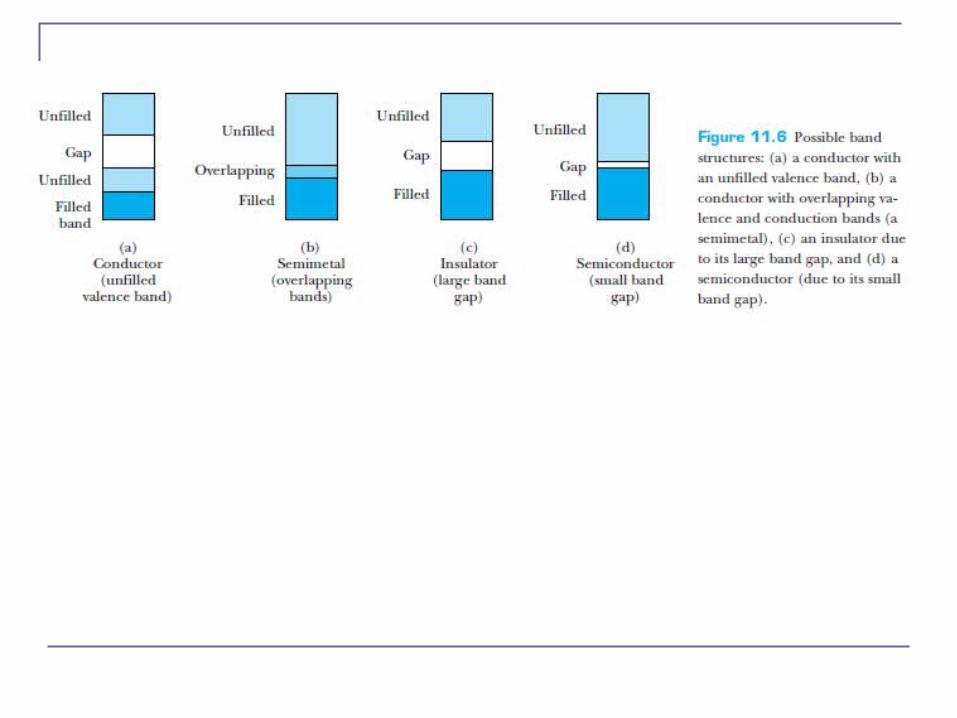
Band Theory and Conductivity
Band theory helps us understand what makes a conductor, insulator, or semiconductor.
1) Good conductors like copper can be understood using the free electron.
2) It is also possible to make a conductor using a material with its highest band filled, in which case no electron in that band can be considered free.
3) If this filled band overlaps with the next higher band, however (so that effectively there is no gap between these two bands) then an applied electric field can make an electron from the filled band jump to the higher level.
This allows conduction to take place, although typically with slightly higher resistance than in normal metals. Such materials are known as semimetals.
Valence and Conduction Bands
The band structures of insulators and semiconductors resemble each other qualitatively. Normally there exists in both insulators and semiconductors a filled energy band (referred to as the valence band) separated from the next higher band (referred to as the conduction band) by an energy gap.
If this gap is at least several electron volts, the material is an insulator. It is too difficult for an applied field to overcome that large an energy gap, and thermal excitations lack the energy to promote sufficient numbers of electrons to the conduction band.
For energy gaps smaller than about 1 electron volt, it is possible for enough electrons to be excited thermally into the conduction band, so that an applied electric field can produce a modest current.
The result is a semiconductor.
Smaller energy gaps create semiconductors
11.4: Nanotechnology
Nanotechnology is generally defined as the scientific study and manufacture of materials on a submicron scale.
These scales range from single atoms (on the order of 0.1 nm up to 1 micron (1000 nm).
This technology has applications in engineering, chemistry, and the life sciences and, as such, is interdisciplinary.
Carbon Nanotubes
In 1991, following the discovery of C60 buckminsterfullerenes, or “buckyballs,” Japanese physicist Sumio Iijima discovered a new geometric arrangement of pure carbon into large molecules.
In this arrangement, known as a carbon nanotube, hexagonal arrays of carbon atoms lie along a cylindrical tube instead of a spherical ball.
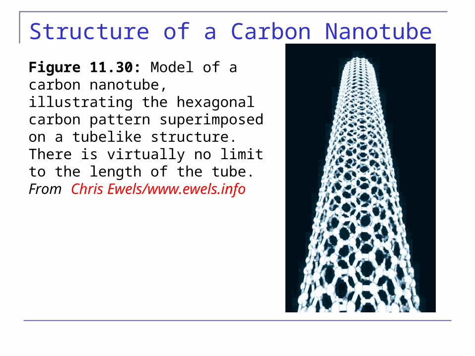
Structure of a Carbon Nanotube
Figure 11.30: Model of a carbon nanotube, illustrating the hexagonal carbon pattern superimposed on a tubelike structure. There is virtually no limit to the length of the tube. From Chris Ewels/www.ewels.info
Carbon Nanotubes
The basic structure shown in Figure 11.30 leads to two types of nanotubes. A single-walled nanotube has just the single shell of hexagons as shown.
In a multi-walled nanotube, multiple layers are nested like the rings in a tree trunk.
Single-walled nanotubes tend to have fewer defects, and they are therefore stronger structurally but they are also more expensive and difficult to make.
Applications of Nanotubes
Because of their strength they are used as structural reinforcements in the manufacture of composite materials (batteries in cell-phones use nanotubes in this way)
Nanotubes have very high electrical and thermal conductivities, and as such lead to high current densities in high-temperature superconductors.
Nanoscale Electronics
One problem in the development of truly small-scale electronic devices is that the connecting wires in any circuit need to be as small as possible, so that they do not overwhelm the nanoscale components they connect.
In addition to the nanotubes already described, semiconductor wires (for example indium phosphide) have been fabricated with diameters as small as 5 nm.
Nanoscale Electronics
These nanowires have been shown useful in connecting nanoscale transistors and memory circuits.
These are referred to as nanotransistors.
Graphene
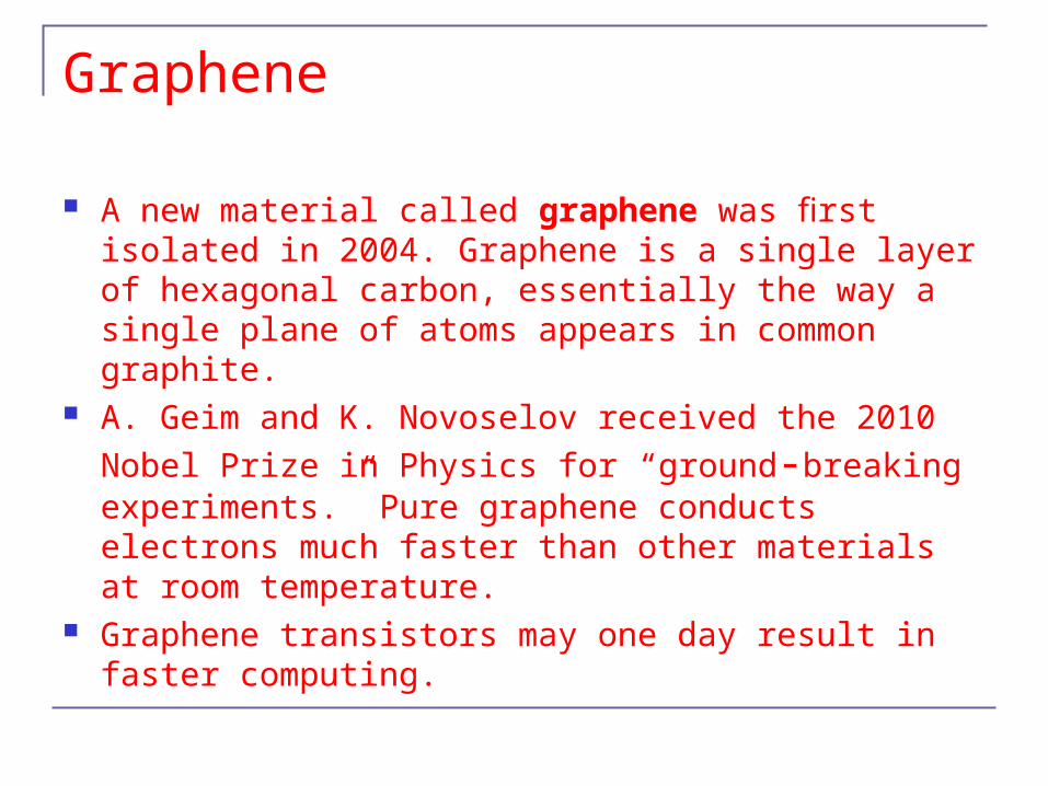
A new material called graphene was first isolated in 2004. Graphene is a single layer of hexagonal carbon, essentially the way a single plane of atoms appears in common graphite.
A. Geim and K. Novoselov received the 2010 Nobel Prize in Physics for “ground-breaking experiments.” Pure graphene conducts electrons much faster than other materials at room temperature.
Graphene transistors may one day result in faster computing.
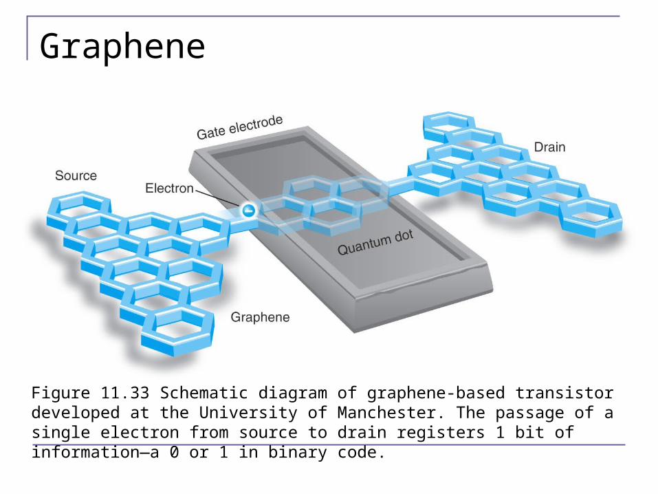
Figure 11.33 Schematic diagram of graphene-based transistor developed at the University of Manchester. The passage of a single electron from source to drain registers 1 bit of information—a 0 or 1 in binary code.
Graphene
Quantum Dots Quantum dots are nanostructures made of
semiconductor materials. They are typically only a few nm across, containing up to 1000
atoms. Each contains an electron-hole pair ]confined within the dot’s
boundaries, (somewhat analogous to a particle confined to a potential well discussed in Chapter 6.
Properties result from the fact that the band gap varies over a wide range and can be controlled precisely by manipulating the quantum dot’s size and shape. They can be made with band gaps that are nearly continuous
throughout the visible light range (1.8 to 3.1 eV) and beyond.
Nanotechnology and the Life Sciences
The complex molecules needed for the variety of life on Earth are themselves examples of nanoscale design.
Examples of unusual materials designed for specific purposes include the molecules that make up claws, feathers, and even tooth enamel.
Information Science
It’s possible that current photolithographic techniques for making computer chips could be extended into the hard-UV or soft x-ray range, with wavelengths on the order of 1 nm, to fabricate silicon-based chips on that scale.
In the 1990s physicists learned that it is possible to take advantage of quantum effects to store and process information more efficiently than a traditional computer. To date, such quantum computers have been built in prototype but not mass-produced.

4-rod Segmented Linear Paul Trap
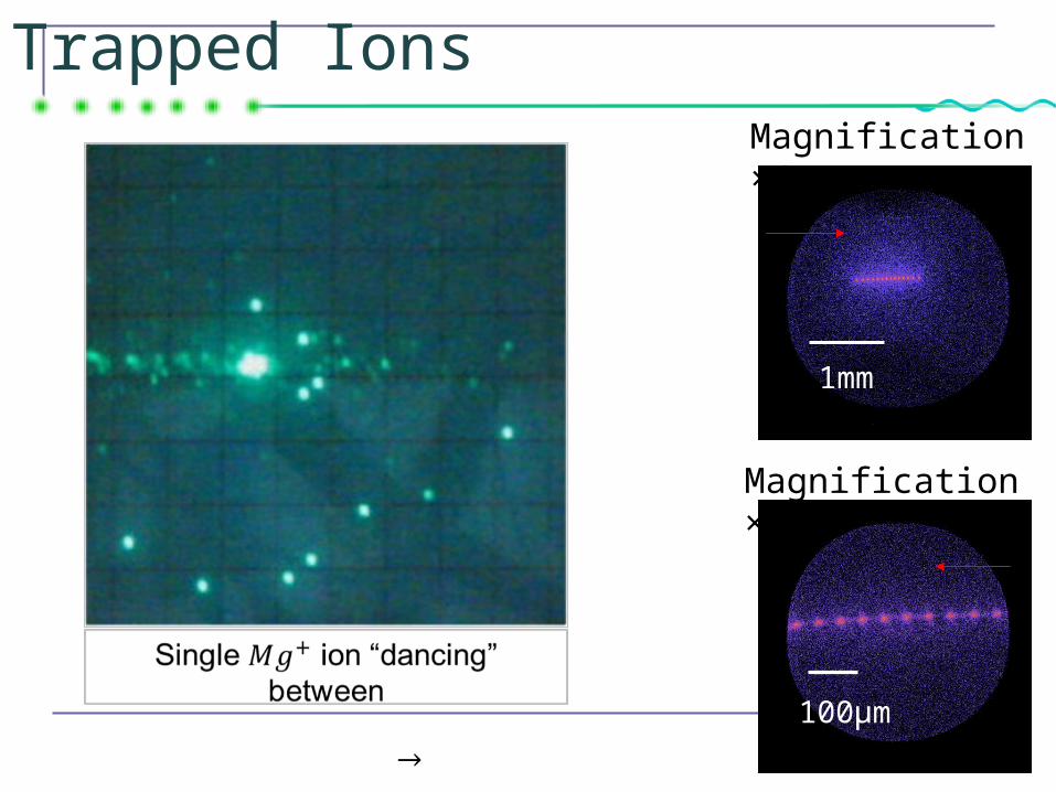
Magnification ×6
1mm
100µm
Magnification ×6 ×8
Trapped Ions