Embed Size (px)
Citation preview
71108 HREM of Interfacial Structures in SemiconductorHetero-StructuresNOBUYUKI IKARASHI* AND KOICHI ISHIDAMicroelectronics Research Laboratories, NEC Corporation, 34 Miyukigaoka Tsukuba 305, Japan
KEY WORDS GaAs/AlAs; Si/Ge; interfacial steps; chemically ordered interface; epitaxial growthmechanism
ABSTRACT We have established a 71108 cross-sectional high-resolution transmission electronmicroscopy (HREM) method to observe atomic structures of semiconductor hetero-interfaces. Weshow theoretically that the semiconductors in a hetero-structure exhibit strong contrast for an EMspecimen thickness near their extinction distances, allowing atomic-scale observations of theinterfacial structures between them. Furthermore, to obtain a clear HREM image, an EM specimenpreparation technique is developed in which chemical etching is used to remove ion milling artifacts.This HREM method allows edge-on imaging of interfaces formed along the 71108 direction;observations of atomic steps at AlAs/GaAs interfaces and a chemically ordered structure at Si/Geinterfaces are demonstrated. Microsc. Res. Tech. 40:187–205, 1998. r 1998 Wiley-Liss, Inc.
INTRODUCTIONAtomic structures of interfaces in semiconductor
hetero-structures dominate electrical and optical prop-erties of the hetero-structures and provide key informa-tion revealing epitaxial crystal growth process (Sakakiet al., 1993). Cross-sectional transmission electron mi-croscopy (TEM) has been widely used to characterizethe hetero-structures (Petroff, 1977; Petroff et al., 1978),and has revealed the structural outlines of the hetero-structures. However, atomic-scale structural analysisof interfaces by HREM has rarely been reported.
For cross-sectional high-resolution TEM (HREM) ofthe interfacial structures, the incident electron beamdirection should be selected so that the structures areobserved edge-on. In HREM of the interfacial atomicstructures, the 71108 is therefore the direction of choice,since various structural characteristics at the inter-faces are often formed in the 71108 direction; atomicsteps at AlAs/GaAs(001) interfaces and an orderedstructure at Si/Ge(001) interfaces are well-known ex-amples. However, 71108 imaging conditions used inprevious experiments were not sufficiently sensitive tothe differences in chemical compositions between semi-conductors making up the interfaces (De Jong et al.,1987; Laval et al., 1987; Poudoulec et al., 1990).
Another serious problem in cross-sectional HREM ofinterfacial structures is noise caused by ion-millingartifacts. Ion milling has been widely used as the finalthinning technique in EM specimen preparation, sinceit etches materials of different compositions (such asGaAs and AlAs) at almost equal etching rates. How-ever, it inevitably produces various artifacts, such aslattice defects, within several nanometers of the speci-men surface (Chew and Cullis, 1987). Noise from theartifacts significantly distorts the lattice image andcauses irregular changes in the background intensitiesof the image, preventing detailed observations of inter-facial structures.
In this paper, first we describe 71108 HREM imagingconditions in which HREM images of semiconductors in
a hetero-structure contrast sharply, allowing atomic-scale observations of the interfacial structures. Thenwe describe an ion-milling artifact-free specimen prepa-ration technique that allows HREM observations. Next,we apply this HREM method to investigate AlAs/GaAsand Si/Ge interfaces; the former are a typical exampleof well lattice-matched hetero-structures (0.1% latticemismatch), and the latter are those of strained hetero-structures (4.0% lattice mismatch).
IMAGING CONDITIONSHere, we describe the HREM image intensity as a
function of imaging conditions in general form. We thendetermine appropriate imaging conditions for AlAs/GaAs interfaces and those for Si/Ge interfaces, usingthe general expressions.
In 71108 imaging of semiconductors, the four 51116beams are the lowest order diffracted beams. Hence,the intensity produced by the interference between the(000) and the four 51116 beams dominates HREM latticeimages. The intensity at a point r on the image planeunder partially coherent illumination is expressed inthe general form (Bourret et al., 1978/1979; Desseauxet al., 1977; Glaisher et al., 1989a,b; Ishizuka, 1985),
I(r) 5 I0(r) 1 I1(r) 1 I2(r), (1)
where I0(r), I1(r), and I2(r) are
I0(r) 5 oi 5 0–4
C0(gi, gi; e),
I1(r) 5 oi 5 1–4
C1(gi, 0; e) exp (22pigi · r), (2)
I2(r) 5 oi Þ 0
oj Þ 0, j Þ i
C2(gi, gj; e) exp (22p i(gi 2 gj ) · r),
*Correspondence to: Nobuyuki Ikarashi, Microelectronics Research Laborato-ries, NEC Corporation, 34 Miyukigaoka, Tsukuba 305, Japan.
Received 15 March 1996; accepted in revised form 22 April 1996
MICROSCOPY RESEARCH AND TECHNIQUE 40:187–205 (1998)
r 1998 WILEY-LISS, INC.
in which g1, g2, g3 (52g1), and g4 (52g2) represent thereciprocal space coordinates of the four 51116 beams (the(111), (111), (111) and (111) beams, in the [110] projec-tion, respectively), and e is the defocus value used inHREM observation. The coefficients of I1 and I2 in eq.(2) are
C0(gi, gi; e) 5 U(gi)2
C1(gi, 0; e) 5 E(gi, 0; e)
· exp [i(Q(gi) 1 x(gi; e) 2 Q(0) 2 x(0; e))] · U(gi)U(0),
C2(gi, 0; e) 5 E(gi, gj; e)
· exp [i(Q(gi) 1 x(gi; e) 2 Q(gj) 2 x(gj; e))] · U(gi)U(gj),
(3)
Here, E(gi, gj; e) represents the product of the defocus-spread-dependent envelope function and the source-size-dependent envelope function (Ishizuka, 1985), andx(g i; e) is the aberration function. Q(gi) and U(gi) are thephases and amplitude of gi diffracted beam, and theyare functions of the specimen thickness. The underlinedparts in eq. (3) are called the generalized contrast transferfunction (GCTF). For C1 and C2, O # Ch (gi, gj; e) #U(gi)U(gj) (h 5 1,2: i, j 5 0,1,2), since 0 # GCTF # 1from the definition. GCTF does not appear in C0, sinceGCTF ; 1 for C0. The term I0 determines the back-ground intensity, while I1 and I2 describe the latticeimage intensity, with I1 giving the interference between
(000) and 51116, and I2 giving the interference betweenthe 51116 beams.
Equations (1)–(3) shows that interferences with largeCi values (i 5 1, 2) dominate HREM lattice imageformation, and that the maximum of Ci values at eachspecimen thickness are determined by U(gi) values.Consequently, semiconductors making up the interfacewould show large differences in their lattice imageintensities when their U(gi) values are significantlydifferent.
Imaging Conditions for GaAs/AlAsTo find the 71108 HREM imaging conditions for the
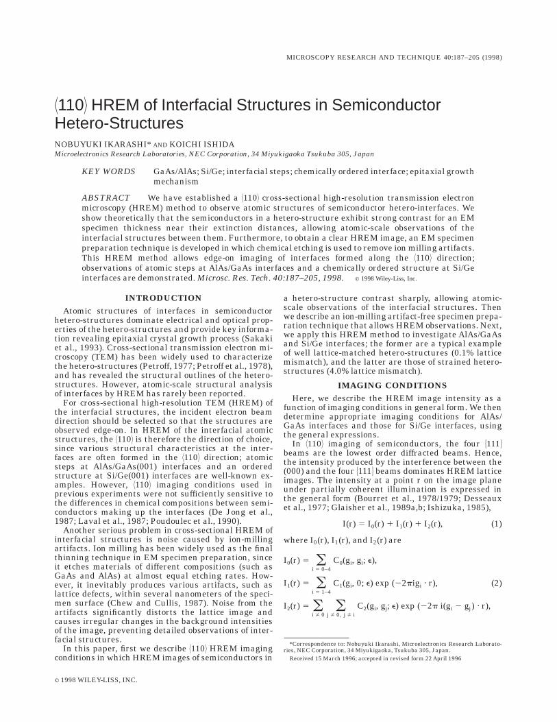
AlAs/GaAs interfaces, we first examine how the 51116beam amplitudes (U(gi), i 5 1–4) change with the thick-ness of GaAs and AlAs specimens, since U(gi) values fora specific material are functions of the specimen thick-ness. Calculated thickness dependencies of the 51116and the (000) beam amplitudes in GaAs and AlAs areshown in Figure 1.1 The multislice method (Cowley andMoodie, 1957) was used in these calculations (accelera-tion voltage: 200 kV). The amplitudes of the 51116 beamsfor GaAs reach a minimum at a thickness near 14.4 nm,whereas the amplitudes forAlAs are significantly higherat this thickness. This remarkable difference in the
1Two solid lines for the 51116 beam amplitudes are shown in each diagram inFig. 1. This is because Bijvoet-related diffracted beams have different thicknessdependencies under dynamical diffraction conditions due to the non-centrosym-metry of the 71108 projection of zincblende crystal structure.
Fig. 1. Variation of 5111]and (000) beam amplitudes with specimen thickness for (a) GaAs and (b) AlAsat 200 kV. The 51116 beams of GaAs are very weak at GaAs extinction distance (14.4-nm specimenthickness), while those for AlAs are significantly higher.
188 N. IKARASHI AND K. ISHIDA
51116 beam amplitudes indicates the possibility of distin-guishing GaAs from AlAs by the difference in theirHREM lattice image intensities; the GaAs lattice imageobtained with a 14.4-nm-thick specimen should appearvery weak, whereas the AlAs image is expected to beclear.
The 14.4-nm specimen thickness for GaAs (the dis-tance where diffracted beams reach the first minimum)is usually called ‘‘the extinction distance’’ of GaAs(jGaAs) (Hirsch et al., 1965). Therefore, the above resultsshow that two materials with different extinction dis-tances in a specimen are expected to show high contrastin the HREM images when the specimen thickness isequivalent to their extinction distances.
The transmitted beam in GaAs (Fig. 1a) is reduced atsample thicknesses of 7.6 and 22.0 nm, and is maxi-mized at 14.4 nm (jGaAs). Since the transmitted beamamplitude dominates the background intensities of thelattice images, the background intensities in a HREMimage of a tapered specimen alternate between brightand dark with increasing specimen thickness. The darkbackground regions appear around 7.6- and 22.0-nmspecimen thicknesses, which are the first and secondthickness fringe, respectively. Therefore, the above-mentioned marked difference in lattice images betweenGaAs and AlAs is expected to be observed around thebright background area between the first and thesecond thickness fringe of GaAs.
Next, we examine the defocus value dependencies ofthe HREM image intensities for GaAs and AlAs at a14.4-nm specimen thickness (jGaAs). Equation 2 showsthat I1 dominates the HREM images of GaAs and AlAs
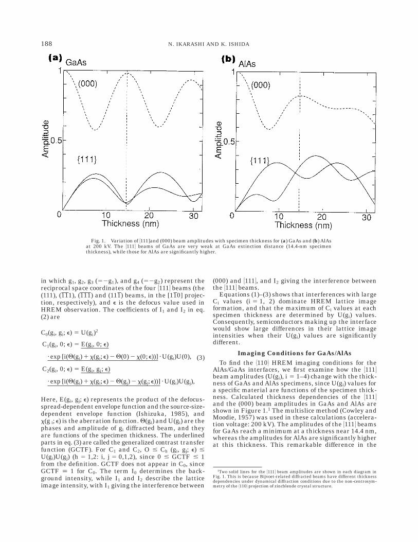
at jGaAs, since I1 is much larger than I2 at jGaAs;U(0)U(gi) 5 6 3 1022 : U(gi)U(gj) 5 3 3 1023 for i, j 51–4, i Þ j in GaAs, and U(0)U(gi) 5 2 3 1021 :U(gi)U(gj) 5 6 3 1023 to 9 3 1023 in AlAs. Hence, thedefocus value dependencies of the HREM images arecharacterized by C1 values as a function of the defocusvalue. The variations in C1 values with specimenthicknesses for GaAs and AlAs around jGaAs are shownin Figure 2. The parameters used in this image inten-sity analysis were 200 kV acceleration voltage, 0.4 mmspherical aberration, 6.4 nm defocus spread, and 5.0mrad beam divergence. These parameters were chosento fit the imaging conditions of the TOPCON EM-002Belectron microscope used in the experiment. The valuesof the phases and amplitudes of the diffracted beamsused in this analysis were obtained by using multislicecalculations. In Figure 2, the solid lines show thedefocus value dependencies of C1 for AlAs around jGaAs(specimen thicknesses of 12.8, 13.6, 14.4, 15.2, and 16.0nm are shown), and the dashed lines show those forGaAs. The results indicate that the GaAs lattice imageare very weak, around 210 nm (the minus sign indi-cates the under-focus condition), while the AlAs latticeimage appears strong between 215 and 220 nm.Therefore, AlAs and GaAs exhibit remarkable contrastin HREM lattice image intensity near a 14.4-nm speci-men thickness and a focus-setting of 210 to 220 nm.
Simulated Images of AlAs/GaAsFigure 3 shows the results of through-focal and
through-thickness image simulations near the above-mentioned imaging conditions. We used an atomic
Fig. 2. Defocus value dependencies of 51116lattice image spectra C1 for GaAs (dashed lines)and AlAs (solid lines) around jGaAs (specimenthicknesses of 12.8, 13.6, 14.4, 15.2, and 16.0nm). Around 210 to 220 nm defocus-setting,absolute value of C1 for GaAs is around zero,while that for AlAs appears strong.
189,110. HREM METHOD

Fig
.3.
Sim
ula
ted
thro
ugh
-foc
alan
dth
rou
gh-t
hic
knes
sim
ages
of[(
AlA
s)1M
L/(
GaA
s)19
ML
s].
GaA
sla
ttic
eim
ages
are
very
wea
kat
asp
ecim
enth
ickn
ess
of14
.4n
m.I
mag
esof
GaA
san
dA
lAs
show
hig
hes
tco
ntr
ast
ata
thic
knes
sof
14.4
nm
and
ade
focu
sof
210
nm
.
190 N. IKARASHI AND K. ISHIDA
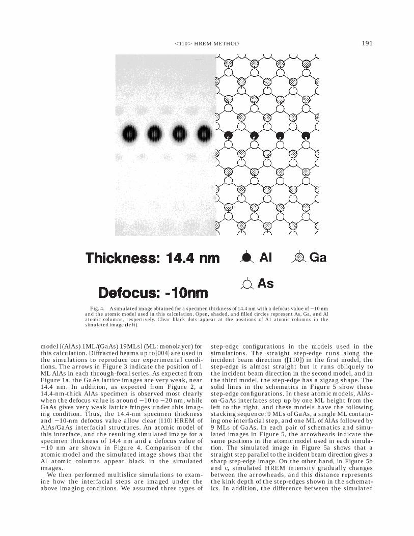
model [(AlAs) 1ML/(GaAs) 19MLs] (ML: monolayer) forthis calculation. Diffracted beams up to 50046 are used inthe simulations to reproduce our experimental condi-tions. The arrows in Figure 3 indicate the position of 1ML AlAs in each through-focal series. As expected fromFigure 1a, the GaAs lattice images are very weak, near14.4 nm. In addition, as expected from Figure 2, a14.4-nm-thick AlAs specimen is observed most clearlywhen the defocus value is around 210 to 220 nm, whileGaAs gives very weak lattice fringes under this imag-ing condition. Thus, the 14.4-nm specimen thicknessand 210-nm defocus value allow clear 71108 HREM ofAlAs/GaAs interfacial structures. An atomic model ofthis interface, and the resulting simulated image for aspecimen thickness of 14.4 nm and a defocus value of210 nm are shown in Figure 4. Comparison of theatomic model and the simulated image shows that theAl atomic columns appear black in the simulatedimages.
We then performed multislice simulations to exam-ine how the interfacial steps are imaged under theabove imaging conditions. We assumed three types of
step-edge configurations in the models used in thesimulations. The straight step-edge runs along theincident beam direction ([110]) in the first model, thestep-edge is almost straight but it runs obliquely tothe incident beam direction in the second model, and inthe third model, the step-edge has a zigzag shape. Thesolid lines in the schematics in Figure 5 show thesestep-edge configurations. In these atomic models, AlAs-on-GaAs interfaces step up by one ML height from theleft to the right, and these models have the followingstacking sequence: 9 MLs of GaAs, a single ML contain-ing one interfacial step, and one ML of AlAs followed by9 MLs of GaAs. In each pair of schematics and simu-lated images in Figure 5, the arrowheads indicate thesame positions in the atomic model used in each simula-tion. The simulated image in Figure 5a shows that astraight step parallel to the incident beam direction gives asharp step-edge image. On the other hand, in Figure 5band c, simulated HREM intensity gradually changesbetween the arrowheads, and this distance representsthe kink depth of the step-edges shown in the schemat-ics. In addition, the difference between the simulated
Fig. 4. A simulated image obtained for a specimen thickness of 14.4 nm with a defocus value of 210 nmand the atomic model used in this calculation. Open, shaded, and filled circles represent As, Ga, and Alatomic columns, respectively. Clear black dots appear at the positions of A1 atomic columns in thesimulated image (left).
191,110. HREM METHOD
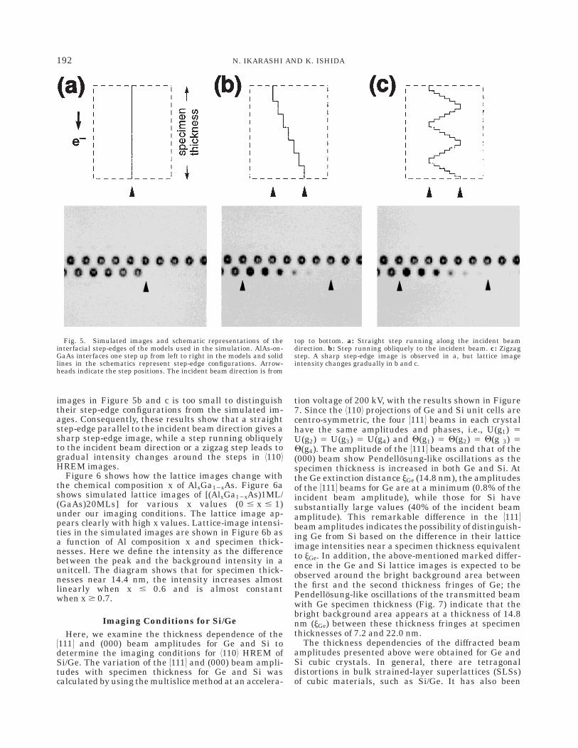
images in Figure 5b and c is too small to distinguishtheir step-edge configurations from the simulated im-ages. Consequently, these results show that a straightstep-edge parallel to the incident beam direction gives asharp step-edge image, while a step running obliquelyto the incident beam direction or a zigzag step leads togradual intensity changes around the steps in 71108HREM images.
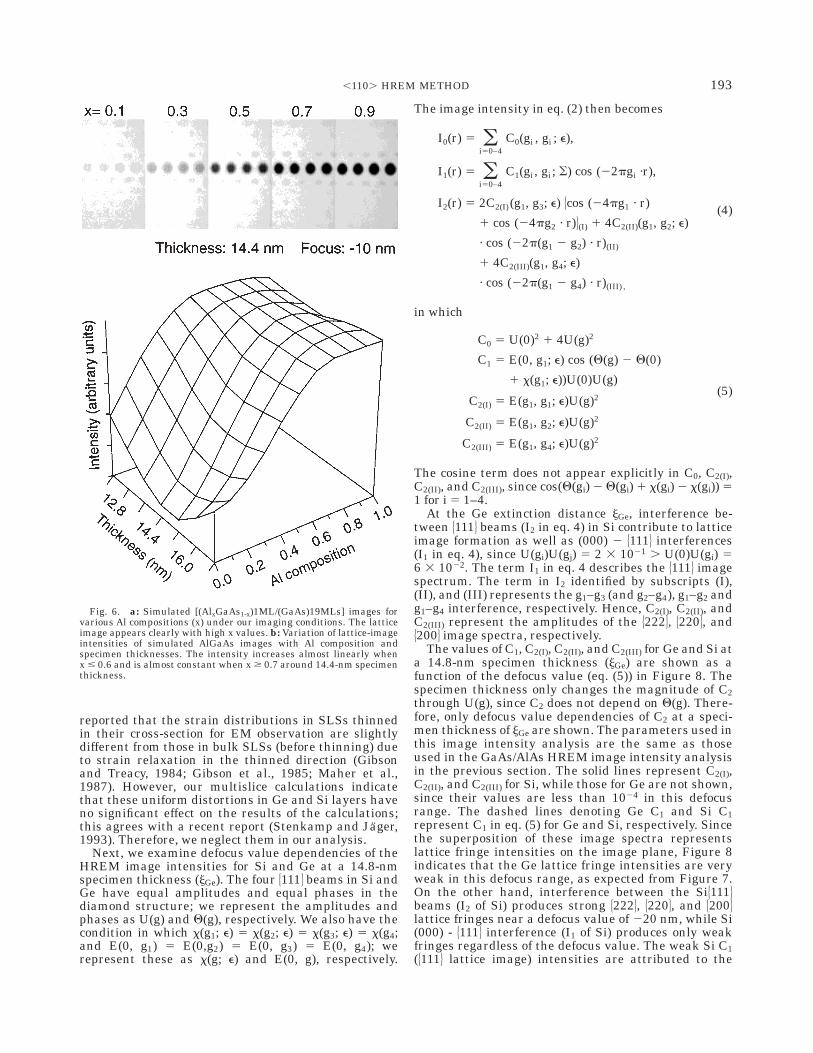
Figure 6 shows how the lattice images change withthe chemical composition x of AlxGa12xAs. Figure 6ashows simulated lattice images of [(AlxGa12xAs)1ML/(GaAs)20MLs] for various x values (0 # x # 1)under our imaging conditions. The lattice image ap-pears clearly with high x values. Lattice-image intensi-ties in the simulated images are shown in Figure 6b asa function of Al composition x and specimen thick-nesses. Here we define the intensity as the differencebetween the peak and the background intensity in aunitcell. The diagram shows that for specimen thick-nesses near 14.4 nm, the intensity increases almostlinearly when x # 0.6 and is almost constantwhen x $ 0.7.
Imaging Conditions for Si/GeHere, we examine the thickness dependence of the
51116 and (000) beam amplitudes for Ge and Si todetermine the imaging conditions for 71108 HREM ofSi/Ge. The variation of the 51116 and (000) beam ampli-tudes with specimen thickness for Ge and Si wascalculated by using the multislice method at an accelera-
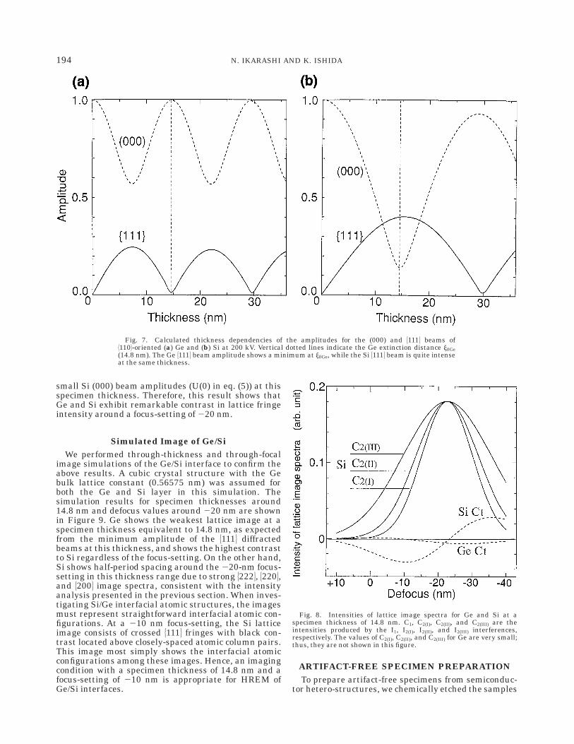
tion voltage of 200 kV, with the results shown in Figure7. Since the 71108 projections of Ge and Si unit cells arecentro-symmetric, the four 51116 beams in each crystalhave the same amplitudes and phases, i.e., U(g1) 5U(g2) 5 U(g3) 5 U(g4) and Q(g1) 5 Q(g2) 5 Q(g 3) 5Q(g4). The amplitude of the 51116 beams and that of the(000) beam show Pendellosung-like oscillations as thespecimen thickness is increased in both Ge and Si. Atthe Ge extinction distance jGe (14.8 nm), the amplitudesof the 51116 beams for Ge are at a minimum (0.8% of theincident beam amplitude), while those for Si havesubstantially large values (40% of the incident beamamplitude). This remarkable difference in the 51116beam amplitudes indicates the possibility of distinguish-ing Ge from Si based on the difference in their latticeimage intensities near a specimen thickness equivalentto jGe. In addition, the above-mentioned marked differ-ence in the Ge and Si lattice images is expected to beobserved around the bright background area betweenthe first and the second thickness fringes of Ge; thePendellosung-like oscillations of the transmitted beamwith Ge specimen thickness (Fig. 7) indicate that thebright background area appears at a thickness of 14.8nm (jGe) between these thickness fringes at specimenthicknesses of 7.2 and 22.0 nm.
The thickness dependencies of the diffracted beamamplitudes presented above were obtained for Ge andSi cubic crystals. In general, there are tetragonaldistortions in bulk strained-layer superlattices (SLSs)of cubic materials, such as Si/Ge. It has also been
Fig. 5. Simulated images and schematic representations of theinterfacial step-edges of the models used in the simulation. AlAs-on-GaAs interfaces one step up from left to right in the models and solidlines in the schematics represent step-edge configurations. Arrow-heads indicate the step positions. The incident beam direction is from
top to bottom. a: Straight step running along the incident beamdirection. b: Step running obliquely to the incident beam. c: Zigzagstep. A sharp step-edge image is observed in a, but lattice imageintensity changes gradually in b and c.
192 N. IKARASHI AND K. ISHIDA
reported that the strain distributions in SLSs thinnedin their cross-section for EM observation are slightlydifferent from those in bulk SLSs (before thinning) dueto strain relaxation in the thinned direction (Gibsonand Treacy, 1984; Gibson et al., 1985; Maher et al.,1987). However, our multislice calculations indicatethat these uniform distortions in Ge and Si layers haveno significant effect on the results of the calculations;this agrees with a recent report (Stenkamp and Jager,1993). Therefore, we neglect them in our analysis.
Next, we examine defocus value dependencies of theHREM image intensities for Si and Ge at a 14.8-nmspecimen thickness (jGe). The four 51116 beams in Si andGe have equal amplitudes and equal phases in thediamond structure; we represent the amplitudes andphases as U(g) and Q(g), respectively. We also have thecondition in which x(g1; e) 5 x(g2; e) 5 x(g3; e) 5 x(g4;and E(0, g1) 5 E(0,g2) 5 E(0, g3) 5 E(0, g4); werepresent these as x(g; e) and E(0, g), respectively.
The image intensity in eq. (2) then becomes
I0(r) 5 oi50–4
C0(gi , gi ; e),
I1(r) 5 oi50–4
C1(gi , gi ; o) cos (22pgi ·r),
I2(r) 5 2C2(I) (g1, g3; e) 5cos (24pg1 · r)
1 cos (24pg2 · r)6(I) 1 4C2(II)(g1, g2; e)
· cos (22p(g1 2 g2) · r)(II)
1 4C2(III)(g1, g4; e)
· cos (22p(g1 2 g4) · r)(III) ,
(4)
in which
C0 5 U(0)2 1 4U(g)2
C1 5 E(0, g1; e) cos (Q(g) 2 Q(0)
1 x(g1; e))U(0)U(g)
C2(I) 5 E(g1, g1; e)U(g)2
C2(II) 5 E(g1, g2; e)U(g)2
C2(III) 5 E(g1, g4; e)U(g)2
(5)
The cosine term does not appear explicitly in C0, C2(I),C2(II), and C2(III), since cos(Q(gi) 2 Q(gi) 1 x(gi) 2 x(gi)) 51 for i 5 1–4.
At the Ge extinction distance jGe, interference be-tween 51116 beams (I2 in eq. 4) in Si contribute to latticeimage formation as well as (000) 2 51116 interferences(I1 in eq. 4), since U(gi)U(gj) 5 2 3 1021 . U(0)U(gi) 56 3 1022. The term I1 in eq. 4 describes the 51116 imagespectrum. The term in I2 identified by subscripts (I),(II), and (III) represents the g1–g3 (and g2–g4), g1–g2 andg1–g4 interference, respectively. Hence, C2(I), C2(II), andC2(III) represent the amplitudes of the 52226, 52206, and52006 image spectra, respectively.
The values of C1, C2(I), C2(II), and C2(III) for Ge and Si ata 14.8-nm specimen thickness (jGe) are shown as afunction of the defocus value (eq. (5)) in Figure 8. Thespecimen thickness only changes the magnitude of C2through U(g), since C2 does not depend on Q(g). There-fore, only defocus value dependencies of C2 at a speci-men thickness of jGe are shown. The parameters used inthis image intensity analysis are the same as thoseused in the GaAs/AlAs HREM image intensity analysisin the previous section. The solid lines represent C2(I),C2(II), and C2(III) for Si, while those for Ge are not shown,since their values are less than 1024 in this defocusrange. The dashed lines denoting Ge C1 and Si C1represent C1 in eq. (5) for Ge and Si, respectively. Sincethe superposition of these image spectra representslattice fringe intensities on the image plane, Figure 8indicates that the Ge lattice fringe intensities are veryweak in this defocus range, as expected from Figure 7.On the other hand, interference between the Si51116beams (I2 of Si) produces strong 52226, 52206, and 52006lattice fringes near a defocus value of 220 nm, while Si(000) - 51116 interference (I1 of Si) produces only weakfringes regardless of the defocus value. The weak Si C1(51116 lattice image) intensities are attributed to the
Fig. 6. a: Simulated [(AlxGaAs1-x)1ML/(GaAs)19MLs] images forvarious Al compositions (x) under our imaging conditions. The latticeimage appears clearly with high x values. b: Variation of lattice-imageintensities of simulated AlGaAs images with Al composition andspecimen thicknesses. The intensity increases almost linearly whenx # 0.6 and is almost constant when x $ 0.7 around 14.4-nm specimenthickness.
193,110. HREM METHOD
small Si (000) beam amplitudes (U(0) in eq. (5)) at thisspecimen thickness. Therefore, this result shows thatGe and Si exhibit remarkable contrast in lattice fringeintensity around a focus-setting of 220 nm.
Simulated Image of Ge/SiWe performed through-thickness and through-focal
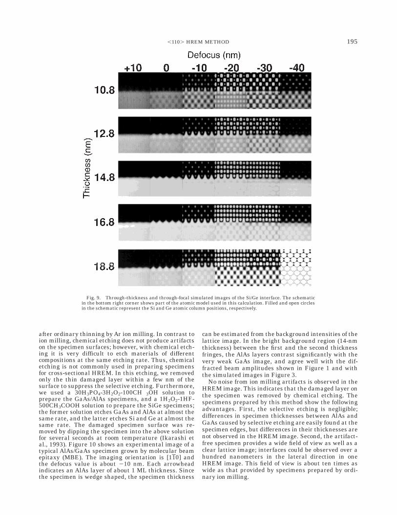
image simulations of the Ge/Si interface to confirm theabove results. A cubic crystal structure with the Gebulk lattice constant (0.56575 nm) was assumed forboth the Ge and Si layer in this simulation. Thesimulation results for specimen thicknesses around14.8 nm and defocus values around 220 nm are shownin Figure 9. Ge shows the weakest lattice image at aspecimen thickness equivalent to 14.8 nm, as expectedfrom the minimum amplitude of the 51116 diffractedbeams at this thickness, and shows the highest contrastto Si regardless of the focus-setting. On the other hand,Si shows half-period spacing around the 220-nm focus-setting in this thickness range due to strong 52226, 52206,and 52006 image spectra, consistent with the intensityanalysis presented in the previous section. When inves-tigating Si/Ge interfacial atomic structures, the imagesmust represent straightforward interfacial atomic con-figurations. At a 210 nm focus-setting, the Si latticeimage consists of crossed 51116 fringes with black con-trast located above closely-spaced atomic column pairs.This image most simply shows the interfacial atomicconfigurations among these images. Hence, an imagingcondition with a specimen thickness of 14.8 nm and afocus-setting of 210 nm is appropriate for HREM ofGe/Si interfaces.
ARTIFACT-FREE SPECIMEN PREPARATIONTo prepare artifact-free specimens from semiconduc-
tor hetero-structures, we chemically etched the samples
Fig. 7. Calculated thickness dependencies of the amplitudes for the (000) and 51116 beams of71108-oriented (a) Ge and (b) Si at 200 kV. Vertical dotted lines indicate the Ge extinction distance j0Ge(14.8 nm). The Ge 51116 beam amplitude shows a minimum at j0Ge, while the Si 51116 beam is quite intenseat the same thickness.
Fig. 8. Intensities of lattice image spectra for Ge and Si at aspecimen thickness of 14.8 nm. C1, C2(I), C2(II), and C2(III) are theintensities produced by the I1, I2(I), I2(II), and I2(III) interferences,respectively. The values of C2(I), C2(II), and C2(III) for Ge are very small;thus, they are not shown in this figure.
194 N. IKARASHI AND K. ISHIDA
after ordinary thinning by Ar ion milling. In contrast toion milling, chemical etching does not produce artifactson the specimen surfaces; however, with chemical etch-ing it is very difficult to etch materials of differentcompositions at the same etching rate. Thus, chemicaletching is not commonly used in preparing specimensfor cross-sectional HREM. In this etching, we removedonly the thin damaged layer within a few nm of thesurface to suppress the selective etching. Furthermore,we used a 30H3PO4-3H2O2-100CH 3OH solution toprepare the GaAs/AlAs specimens, and a 1H2O2-1HF-500CH3COOH solution to prepare the SiGe specimens;the former solution etches GaAs and AlAs at almost thesame rate, and the latter etches Si and Ge at almost thesame rate. The damaged specimen surface was re-moved by dipping the specimen into the above solutionfor several seconds at room temperature (Ikarashi etal., 1993). Figure 10 shows an experimental image of atypical AlAs/GaAs specimen grown by molecular beamepitaxy (MBE). The imaging orientation is [110] andthe defocus value is about 210 nm. Each arrowheadindicates an AlAs layer of about 1 ML thickness. Sincethe specimen is wedge shaped, the specimen thickness
can be estimated from the background intensities of thelattice image. In the bright background region (14-nmthickness) between the first and the second thicknessfringes, the AlAs layers contrast significantly with thevery weak GaAs image, and agree well with the dif-fracted beam amplitudes shown in Figure 1 and withthe simulated images in Figure 3.
No noise from ion milling artifacts is observed in theHREM image. This indicates that the damaged layer onthe specimen was removed by chemical etching. Thespecimens prepared by this method show the followingadvantages. First, the selective etching is negligible;differences in specimen thicknesses between AlAs andGaAs caused by selective etching are easily found at thespecimen edges, but differences in their thicknesses arenot observed in the HREM image. Second, the artifact-free specimen provides a wide field of view as well as aclear lattice image; interfaces could be observed over ahundred nanometers in the lateral direction in oneHREM image. This field of view is about ten times aswide as that provided by specimens prepared by ordi-nary ion milling.
Fig. 9. Through-thickness and through-focal simulated images of the Si/Ge interface. The schematicin the bottom right corner shows part of the atomic model used in this calculation. Filled and open circlesin the schematic represent the Si and Ge atomic column positions, respectively.
195,110. HREM METHOD

HREM OF AlAs/GaAs INTERFACIALSTRUCTURES
In this section, we describe studies of AlAs/GaAsinterfacial structures by our HREM method. We firstshow the interface abruptness of our sample using thechemical composition (X) dependencies of AlxGa1-xAslattice images described in the previous section.
Then we demonstrate the structural differences be-tween interfacial steps along the [110] direction andthose along the [110] direction. The surface steps onGaAs (001) running along the [110] direction are usu-ally referred to as A-steps and those running along the[110] direction are referred to as B-steps. Reflectionhigh-energy electron diffraction (RHEED) observationshave suggested that the straightness of the step edges,and the step interval distributions, differ between thesesteps (Neave et al., 1983; Pukite et al., 1989). We
investigate the structure of these interfacial steps byusing edge-on HREM of vicinal interfaces; A-steps areintroduced at the hetero-interfaces grown on GaAs(001) substrates slightly tilted toward [110], whileB-steps are introduced at the interface grown on thesubstrates tilted toward [110].
Next, we illustrate the effect of growth interruptionon the interface formation during MBE growth. Growthinterruption is a well-known technique that has beenproposed for forming atomically flat interfaces (Fuku-naga et al., 1985; Sakaki et al., 1985). RHEED andphoto-luminescence (PL) studies indicate that thegrowth interruption changes the interface structures aswell as the growth surface structure, suggesting thatgrowth-interrupted interfaces are smoother than thoseprepared by conventional MBE (Sakaki et al., 1985;Tanaka et al., 1986; Tanaka and Sakaki, 1987). How-
Fig. 10. Wide-field-of-view [110] image of a typical EM specimen prepared by the method outlined inthe text. No noise from ion milling artifacts and no evidence of selective etching are observed. Specimenthicknesses estimated from the GaAs thickness fringes are indicated.
196 N. IKARASHI AND K. ISHIDA
ever, direct observations of the differences betweenthese interfaces have not yet been reported.
Interface AbruptnessWe examined the abruptness of AlAs/GaAs interfaces
by using HREM image intensity analysis; we input theHREM images into a personal computer using a videocamera and measured the intensity of each unitcell. A[(AlAs)1ML/(GaAs)100MLs]10 superlattice with a 50-nmcapping layer grown on a GaAs(001) substrate was usedin this experiment. The growth rates of GaAs and AlAswere 1.4 3 1021 and 0.3 3 1021nm/s, respectively. Thesuperlattice was fabricated at 520°C and was cooled to
room temperature within 1 hour from the beginning ofthe superlattice fabrication.
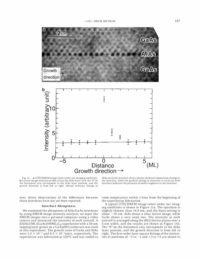
A typical [110] HREM image taken under our imag-ing conditions is shown in Figure 11a. The specimen isslightly thinner than 14.4 nm, and the focus-setting isabout 210 nm. AlAs shows a clear lattice image, whileGaAs shows a very weak one. The intensity at eachunitcell is averaged along the (001) lattice planes over a5-nm width, and the results are shown in Figure 11b.The ‘‘0’’ on the horizontal axis corresponds to the AlAslayer position, and the growth direction is from left toright. The first-order least-square fittings of the intensi-ties at positions of 25 to 21 and 13 to 15 are shown to
Fig. 11. a: [110] HREM image taken under our imaging conditions.b: Lattice-image intensity profile across the AlAs layer. In b, the ‘‘0’’ onthe horizontal axis corresponds to the AlAs layer position, and thegrowth direction is from left to right. Abrupt intensity change at
AlAs-on-GaAs interface shows abrupt chemical composition change atthe interface, while the gradual change in intensity at GaAs-on-AlAsinterface indicates the presence of small roughness at the interface.
197,110. HREM METHOD
indicate the intensities in the GaAs layers. A slightincrease in GaAs intensity is caused by decreasing thespecimen thickness in the growth direction, since thespecimen is slightly thinner than 14.4 nm.
The difference in abruptness between the AlAs-on-GaAs and GaAs-on-AlAs interfaces is evident: a transi-tion region from AlAs to GaAs appears at the 11 and12 positions (GaAs-on-AlAs interface), while no transi-tion layer is observed for AlAs-on-GaAs. In cross-sectional HREM of AlAs/GaAs interfaces, a transitionlayer appears when a compositional transition layer isformed by thermal diffusion of Ga and Al atoms and/orwhen small interfacial roughness in the incident beamdirection causes an intensity transition layer. Ourobserved difference in interfacial abruptness indicatesthat the transition layer at the GaAs-on-AlAs interfaceis mainly caused by the small roughness, since thermaldiffusion should form the same transition layer at bothAlAs-on-GaAs and GaAs-on-AlAs interfaces. The pre-sent results agree with previous PL measurementsconcerning the differences in interfacial roughness be-tweenAlAs-on-GaAs and GaAs-on-AlAs (Tanaka, 1986).
The abrupt intensity change at the AlAs-on-GaAsinterface strongly suggests an abrupt compositionalchange there. We estimated the amount of thermaldiffusion of Al in our sample using the one-dimensionaldiffusion equation and found it to be negligible; thisagreed with our experimental results. The Al composi-tion at the n-th layer at time t, x(n, t), in our sample is
x(n, t) 5Sd
ÎpDtexp 12 (nd)2
4Dt 2 , (6)
where S is the Al composition at the diffusion source, dthe distance between (001) layers, and D the diffusioncoefficient. We set S at 1⁄2 sinceAl diffuses into substrate-side and surface-side GaAs layers, and set d at 0.281nm (the distance between GaAs (001 planes). The
diffusion time t is less than 3,600 s in this experiment.The diffusion constant D at our growth temperature ismuch smaller than 1 3 10220 cm2/s from a previousexperiment (Ourmazd et al., 1990). Consequently, fromeq. 6, the largest Al composition of the GaAs layers atthe 61 position (next to the AlAs layer) is 0.6% in ouras-grown sample. This result indicates that A1 atomshardly diffused into the GaAs layers during the super-lattice fabrication. This is consistent with our HREMresults, which show abrupt compositional change at theAlAs-on-GaAs interface.
Step Structures at GaAs/AlAs Vicinal InterfacesTo determine the step structure of vicinal interfaces,
we examined two superlattice samples grown on GaAs(001) substrates tilted 2° toward (111)A and 2° toward(111)B. These two samples are referred to as sample Aand sample B, respectively, in this section. We exam-ined sample A in the [110] cross-section and sample B inthe [110] cross-section to image the interfacial stepsedge-on. The average interval between neighboring MLsteps on these surfaces is 8 nm. On these substrates wegrew a hetero-structure by alternately depositing oneML of AlAs and 14 MLs of GaAs a total of 20 times.
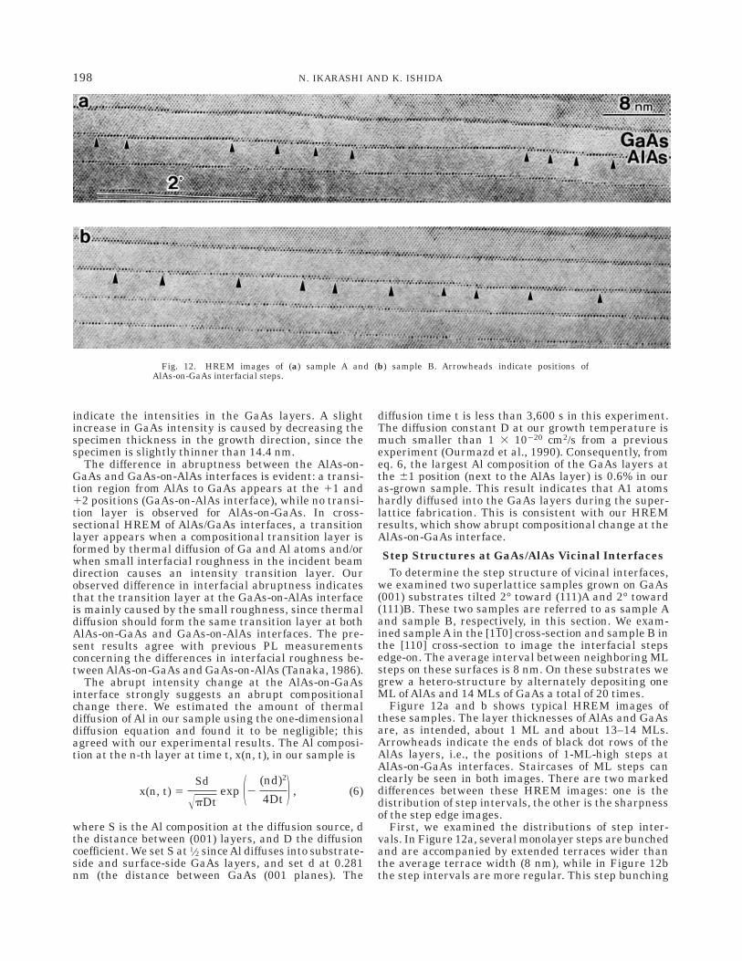
Figure 12a and b shows typical HREM images ofthese samples. The layer thicknesses of AlAs and GaAsare, as intended, about 1 ML and about 13–14 MLs.Arrowheads indicate the ends of black dot rows of theAlAs layers, i.e., the positions of 1-ML-high steps atAlAs-on-GaAs interfaces. Staircases of ML steps canclearly be seen in both images. There are two markeddifferences between these HREM images: one is thedistribution of step intervals, the other is the sharpnessof the step edge images.
First, we examined the distributions of step inter-vals. In Figure 12a, several monolayer steps are bunchedand are accompanied by extended terraces wider thanthe average terrace width (8 nm), while in Figure 12bthe step intervals are more regular. This step bunching
Fig. 12. HREM images of (a) sample A and (b) sample B. Arrowheads indicate positions ofAlAs-on-GaAs interfacial steps.
198 N. IKARASHI AND K. ISHIDA
in sample A usually occurs with several ML steps. Aso-called giant step or a macroscopic step consisting ofmore than several hundred ML steps has never beenfound.
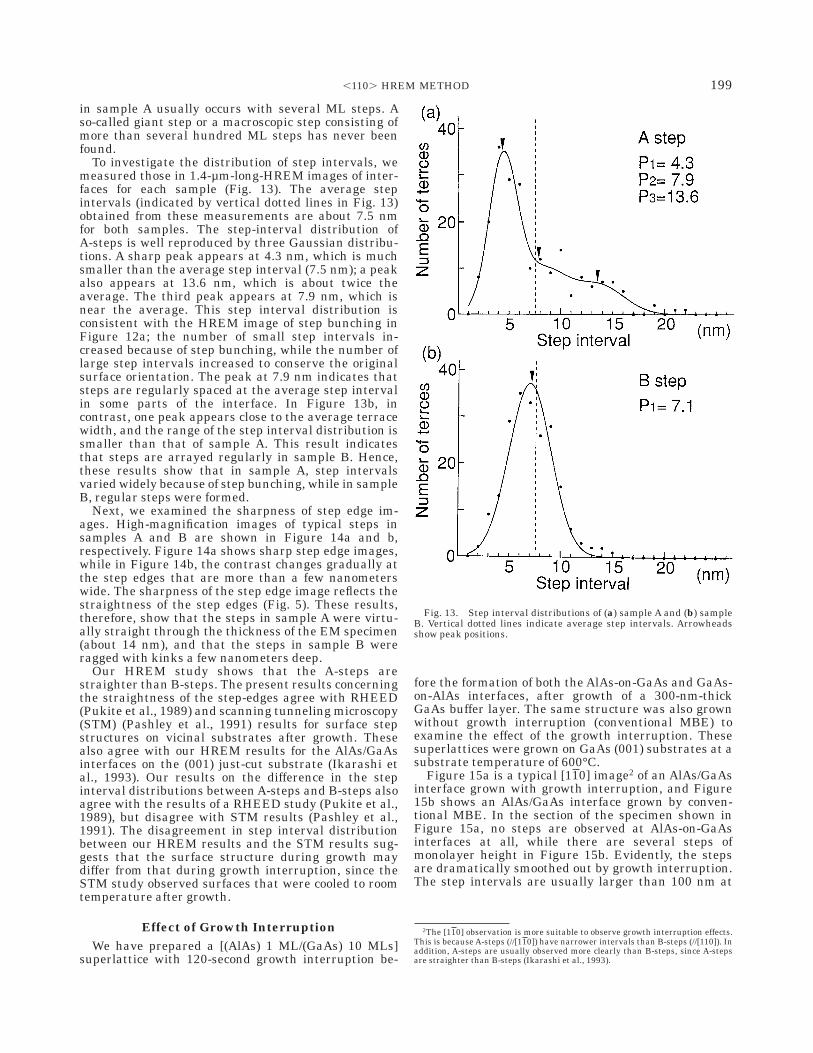
To investigate the distribution of step intervals, wemeasured those in 1.4-µm-long-HREM images of inter-faces for each sample (Fig. 13). The average stepintervals (indicated by vertical dotted lines in Fig. 13)obtained from these measurements are about 7.5 nmfor both samples. The step-interval distribution ofA-steps is well reproduced by three Gaussian distribu-tions. A sharp peak appears at 4.3 nm, which is muchsmaller than the average step interval (7.5 nm); a peakalso appears at 13.6 nm, which is about twice theaverage. The third peak appears at 7.9 nm, which isnear the average. This step interval distribution isconsistent with the HREM image of step bunching inFigure 12a; the number of small step intervals in-creased because of step bunching, while the number oflarge step intervals increased to conserve the originalsurface orientation. The peak at 7.9 nm indicates thatsteps are regularly spaced at the average step intervalin some parts of the interface. In Figure 13b, incontrast, one peak appears close to the average terracewidth, and the range of the step interval distribution issmaller than that of sample A. This result indicatesthat steps are arrayed regularly in sample B. Hence,these results show that in sample A, step intervalsvaried widely because of step bunching, while in sampleB, regular steps were formed.
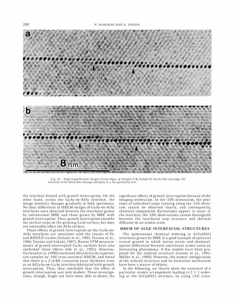
Next, we examined the sharpness of step edge im-ages. High-magnification images of typical steps insamples A and B are shown in Figure 14a and b,respectively. Figure 14a shows sharp step edge images,while in Figure 14b, the contrast changes gradually atthe step edges that are more than a few nanometerswide. The sharpness of the step edge image reflects thestraightness of the step edges (Fig. 5). These results,therefore, show that the steps in sample A were virtu-ally straight through the thickness of the EM specimen(about 14 nm), and that the steps in sample B wereragged with kinks a few nanometers deep.
Our HREM study shows that the A-steps arestraighter than B-steps. The present results concerningthe straightness of the step-edges agree with RHEED(Pukite et al., 1989) and scanning tunneling microscopy(STM) (Pashley et al., 1991) results for surface stepstructures on vicinal substrates after growth. Thesealso agree with our HREM results for the AlAs/GaAsinterfaces on the (001) just-cut substrate (Ikarashi etal., 1993). Our results on the difference in the stepinterval distributions between A-steps and B-steps alsoagree with the results of a RHEED study (Pukite et al.,1989), but disagree with STM results (Pashley et al.,1991). The disagreement in step interval distributionbetween our HREM results and the STM results sug-gests that the surface structure during growth maydiffer from that during growth interruption, since theSTM study observed surfaces that were cooled to roomtemperature after growth.
Effect of Growth InterruptionWe have prepared a [(AlAs) 1 ML/(GaAs) 10 MLs]
superlattice with 120-second growth interruption be-
fore the formation of both the AlAs-on-GaAs and GaAs-on-AlAs interfaces, after growth of a 300-nm-thickGaAs buffer layer. The same structure was also grownwithout growth interruption (conventional MBE) toexamine the effect of the growth interruption. Thesesuperlattices were grown on GaAs (001) substrates at asubstrate temperature of 600°C.
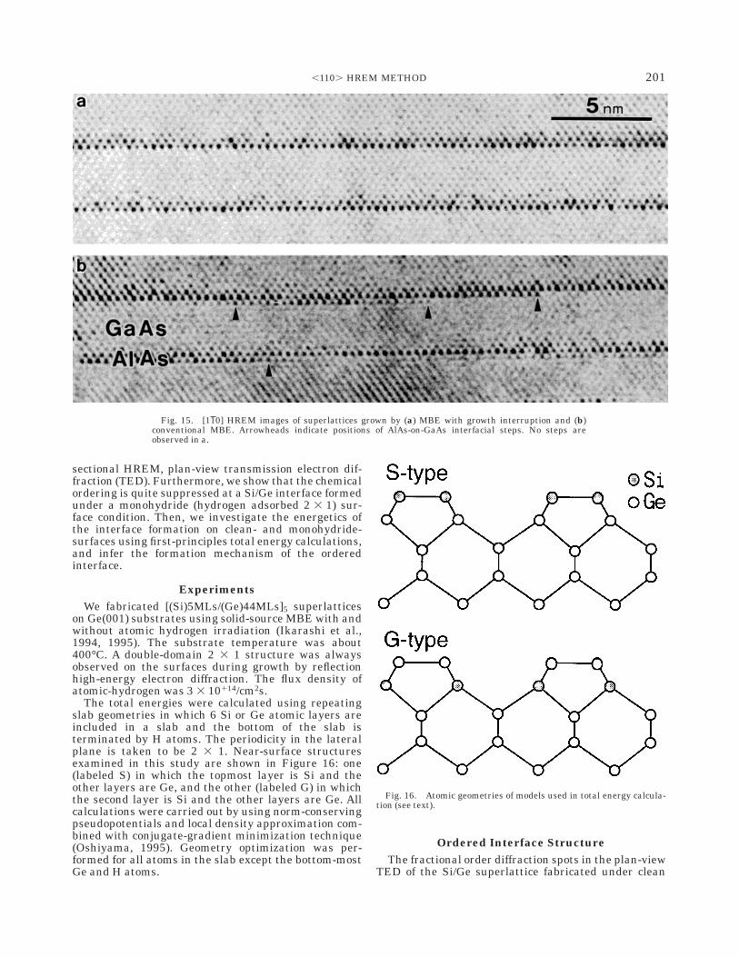
Figure 15a is a typical [110] image2 of an AlAs/GaAsinterface grown with growth interruption, and Figure15b shows an AlAs/GaAs interface grown by conven-tional MBE. In the section of the specimen shown inFigure 15a, no steps are observed at AlAs-on-GaAsinterfaces at all, while there are several steps ofmonolayer height in Figure 15b. Evidently, the stepsare dramatically smoothed out by growth interruption.The step intervals are usually larger than 100 nm at
2The [110] observation is more suitable to observe growth interruption effects.This is because A-steps (//[110]) have narrower intervals than B-steps (//[110]). Inaddition, A-steps are usually observed more clearly than B-steps, since A-stepsare straighter than B-steps (Ikarashi et al., 1993).
Fig. 13. Step interval distributions of (a) sample A and (b) sampleB. Vertical dotted lines indicate average step intervals. Arrowheadsshow peak positions.
199,110. HREM METHOD
the interface formed with growth interruption. On theother hand, across the GaAs-on-AlAs interface, theimage intensity changes gradually in both specimens.No clear differences in HREM images of GaAs-on-AlAsinterfaces were observed between the interfaces grownby conventional MBE and those grown by MBE withgrowth interruption. Thus, growth interruption smoothsout surface steps on the growing GaAs surface, but doesnot noticeably affect the AlAs surface.
These effects of growth interruption on the GaAs-on-AlAs interfaces are consistent with the results of PLand RHEED studies (Sakaki et al., 1985; Tanaka et al.,1986; Tanaka and Sakaki, 1987). Recent STM measure-ments of growth-interrupted GaAs surfaces have alsoconfirmed these effects (Ide et al., 1992). However,Ourmazd et al. (1990) examinedAlGaAs/GaAs superlat-tice samples by 71008 cross-sectional HREM, and foundthat there is a 2–4-ML transition layer thickness evenat an AlGaAs-on-GaAs interface fabricated with growthinterruption. Thus, they concluded that the effect ofgrowth interruption was only modest. These investiga-tions, though, might not have been able to detect the
significant effects of growth interruption because of theimaging orientation. In the 71008 orientation, the posi-tions of individual steps running along the 71108 direc-tion cannot be observed clearly, and consequently,chemical composition fluctuations appear to occur atthe interface; the 71008 observations cannot distinguishbetween the interfacial step structure and thermaldiffusion on an atomic scale.
HREM OF SI/GE INTERFACIAL STRUCTURESThe spontaneous chemical ordering at Si/Ge(001)
interfaces grown by MBE is a good example of epitaxialcrystal growth in which lattice strain and chemical-species differences between constituent atoms cause aninteresting phenomena. A few models have been pro-posed for the ordered structure (Jesson et al., 1991;Muller et al., 1989). However, the atomic configurationof the ordered structure and its formation mechanismhave been a matter of debate.
In the following, we clearly show the existence of aparticular atomic arrangement leading to 2 3 1 order-ing at the Si/Ge(001) interface, by using 71108 cross-
Fig. 14. High magnification images of step edges. a: Sample A. b: Sample B. Across the step edge, theintensity of the black dots changes abruptly in a, but gradually in b.
200 N. IKARASHI AND K. ISHIDA
sectional HREM, plan-view transmission electron dif-fraction (TED). Furthermore, we show that the chemicalordering is quite suppressed at a Si/Ge interface formedunder a monohydride (hydrogen adsorbed 2 3 1) sur-face condition. Then, we investigate the energetics ofthe interface formation on clean- and monohydride-surfaces using first-principles total energy calculations,and infer the formation mechanism of the orderedinterface.
ExperimentsWe fabricated [(Si)5MLs/(Ge)44MLs]5 superlattices
on Ge(001) substrates using solid-source MBE with andwithout atomic hydrogen irradiation (Ikarashi et al.,1994, 1995). The substrate temperature was about400°C. A double-domain 2 3 1 structure was alwaysobserved on the surfaces during growth by reflectionhigh-energy electron diffraction. The flux density ofatomic-hydrogen was 3 3 10114/cm2s.
The total energies were calculated using repeatingslab geometries in which 6 Si or Ge atomic layers areincluded in a slab and the bottom of the slab isterminated by H atoms. The periodicity in the lateralplane is taken to be 2 3 1. Near-surface structuresexamined in this study are shown in Figure 16: one(labeled S) in which the topmost layer is Si and theother layers are Ge, and the other (labeled G) in whichthe second layer is Si and the other layers are Ge. Allcalculations were carried out by using norm-conservingpseudopotentials and local density approximation com-bined with conjugate-gradient minimization technique(Oshiyama, 1995). Geometry optimization was per-formed for all atoms in the slab except the bottom-mostGe and H atoms.
Ordered Interface StructureThe fractional order diffraction spots in the plan-view
TED of the Si/Ge superlattice fabricated under clean
Fig. 16. Atomic geometries of models used in total energy calcula-tion (see text).
Fig. 15. [110] HREM images of superlattices grown by (a) MBE with growth interruption and (b)conventional MBE. Arrowheads indicate positions of AlAs-on-GaAs interfacial steps. No steps areobserved in a.
201,110. HREM METHOD
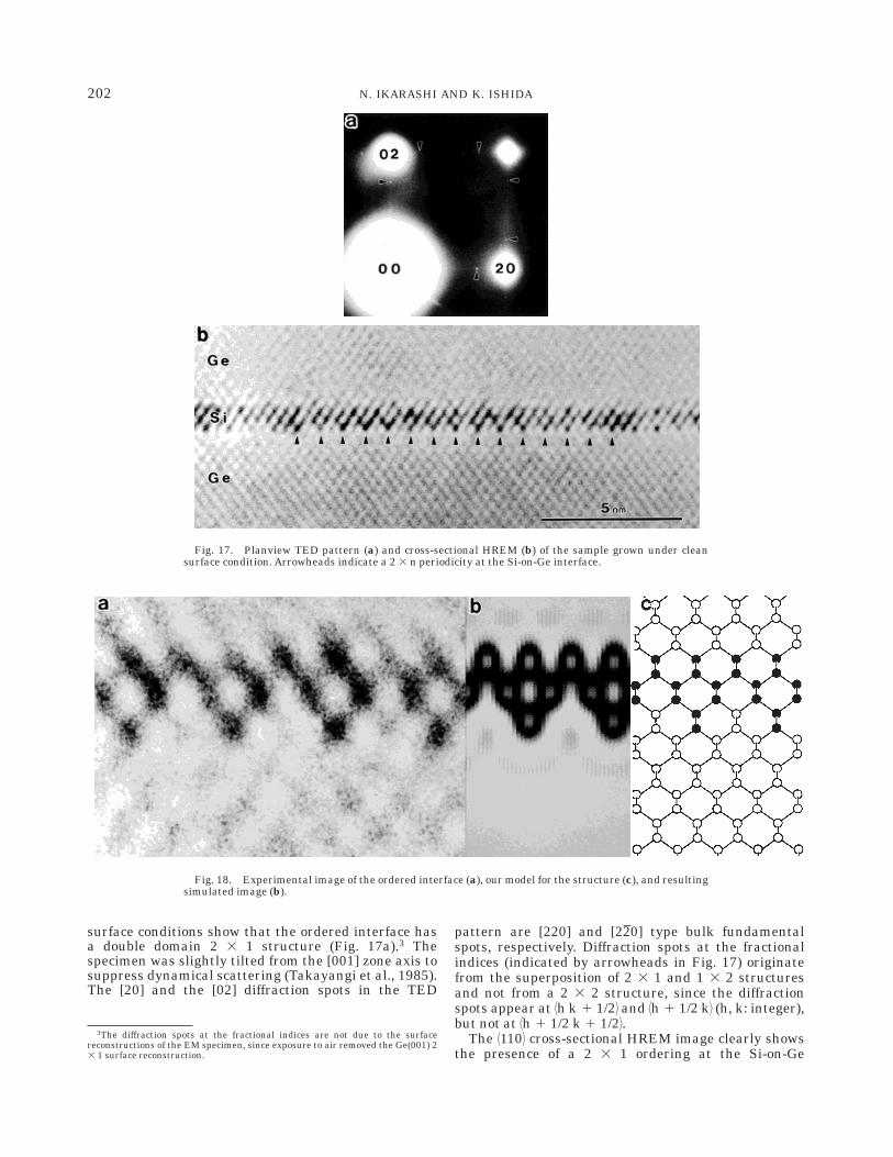
surface conditions show that the ordered interface hasa double domain 2 3 1 structure (Fig. 17a).3 Thespecimen was slightly tilted from the [001] zone axis tosuppress dynamical scattering (Takayangi et al., 1985).The [20] and the [02] diffraction spots in the TED
pattern are [220] and [220] type bulk fundamentalspots, respectively. Diffraction spots at the fractionalindices (indicated by arrowheads in Fig. 17) originatefrom the superposition of 2 3 1 and 1 3 2 structuresand not from a 2 3 2 structure, since the diffractionspots appear at 7h k 1 1/28 and 7h 1 1/2 k8 (h, k: integer),but not at 7h 1 1/2 k 1 1/28.
The 71108 cross-sectional HREM image clearly showsthe presence of a 2 3 1 ordering at the Si-on-Ge
3The diffraction spots at the fractional indices are not due to the surfacereconstructions of the EM specimen, since exposure to air removed the Ge(001) 23 1 surface reconstruction.
Fig. 17. Planview TED pattern (a) and cross-sectional HREM (b) of the sample grown under cleansurface condition. Arrowheads indicate a 2 3 n periodicity at the Si-on-Ge interface.
Fig. 18. Experimental image of the ordered interface (a), our model for the structure (c), and resultingsimulated image (b).
202 N. IKARASHI AND K. ISHIDA
interface (Fig. 17b). The Si layer shows a clear latticeimage, while the Ge lattice image is very weak. TheSi-on-Ge interface shows a periodicity of twice the (110)spacing, as indicated by the arrowheads. The orderedregions often extend over 10 nm in width. Note that theGe-on-Si interface is very nearly abrupt and there is no2 3 1 interfacial ordering. Our model for the 2 3 1ordered interface and the resulting simulated imageare shown in Figure 18, together with a high-magnifica-tion experimental image of the interface. The open andsolid circles show Ge and Si atomic columns, respec-tively. The simulated image reproduces the doubling ofthe (110) periodicity at the Si-on-Ge interface andagrees well with the experimental image.
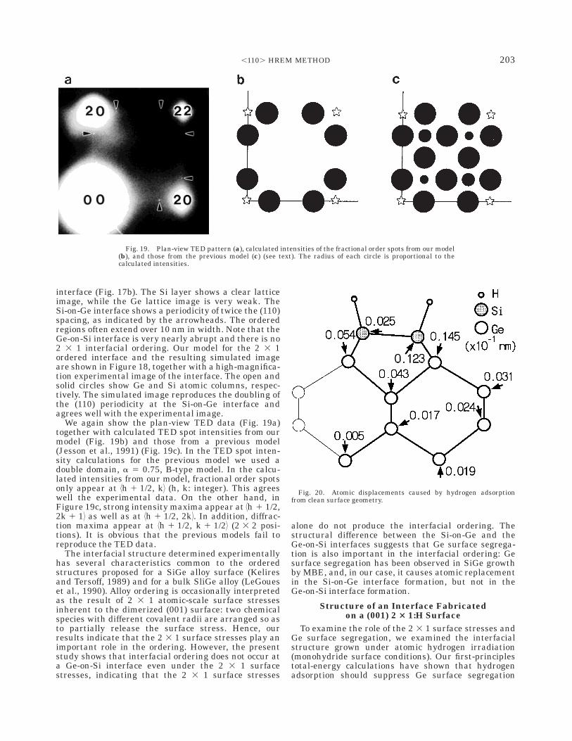
We again show the plan-view TED data (Fig. 19a)together with calculated TED spot intensities from ourmodel (Fig. 19b) and those from a previous model(Jesson et al., 1991) (Fig. 19c). In the TED spot inten-sity calculations for the previous model we used adouble domain, a 5 0.75, B-type model. In the calcu-lated intensities from our model, fractional order spotsonly appear at 7h 1 1/2, k8 (h, k: integer). This agreeswell the experimental data. On the other hand, inFigure 19c, strong intensity maxima appear at 7h 1 1/2,2k 1 18 as well as at 7h 1 1/2, 2k8. In addition, diffrac-tion maxima appear at 7h 1 1/2, k 1 1/28 (2 3 2 posi-tions). It is obvious that the previous models fail toreproduce the TED data.
The interfacial structure determined experimentallyhas several characteristics common to the orderedstructures proposed for a SiGe alloy surface (Keliresand Tersoff, 1989) and for a bulk SliGe alloy (LeGoueset al., 1990). Alloy ordering is occasionally interpretedas the result of 2 3 1 atomic-scale surface stressesinherent to the dimerized (001) surface: two chemicalspecies with different covalent radii are arranged so asto partially release the surface stress. Hence, ourresults indicate that the 2 3 1 surface stresses play animportant role in the ordering. However, the presentstudy shows that interfacial ordering does not occur ata Ge-on-Si interface even under the 2 3 1 surfacestresses, indicating that the 2 3 1 surface stresses
alone do not produce the interfacial ordering. Thestructural difference between the Si-on-Ge and theGe-on-Si interfaces suggests that Ge surface segrega-tion is also important in the interfacial ordering: Gesurface segregation has been observed in SiGe growthby MBE, and, in our case, it causes atomic replacementin the Si-on-Ge interface formation, but not in theGe-on-Si interface formation.
Structure of an Interface Fabricatedon a (001) 2 3 1:H Surface
To examine the role of the 2 3 1 surface stresses andGe surface segregation, we examined the interfacialstructure grown under atomic hydrogen irradiation(monohydride surface conditions). Our first-principlestotal-energy calculations have shown that hydrogenadsorption should suppress Ge surface segregation
Fig. 20. Atomic displacements caused by hydrogen adsorptionfrom clean surface geometry.
Fig. 19. Plan-view TED pattern (a), calculated intensities of the fractional order spots from our model(b), and those from the previous model (c) (see text). The radius of each circle is proportional to thecalculated intensities.
203,110. HREM METHOD
during Si-on-Ge interface formation, leaving atomic-scale surface stresses almost unchanged. Our calcula-tions show that, first, the total energy of the G-typestructure is lower than that of the S-type structure by0.31 eV per surface dimer under a clean surface condi-tion, i.e., Ge surface segregation lowers the total energy.This explains Ge surface segregation in terms of ener-getics. For monohydride surfaces, on the other hand,the total energy increases by 0.19 eV with the exchangeof sub-surface Ge and top-layer Si. This indicates thatGe surface segregation is suppressed on monohydridesurfaces. A schematic view of the stable monohydrideS-type structure is shown in Figure 20. The directionsand the magnitudes of the displacement compared withthe clean-surface geometry are also shown. The atomschange their position in 71108 planes parallel to thesurface dimer. However, the magnitudes of the displace-ments are typically less than 0.01 nm and are verysmall. Thus, this result indicates that the 2 3 1 surfacestresses remain almost unchanged by hydrogen adsorp-tion.
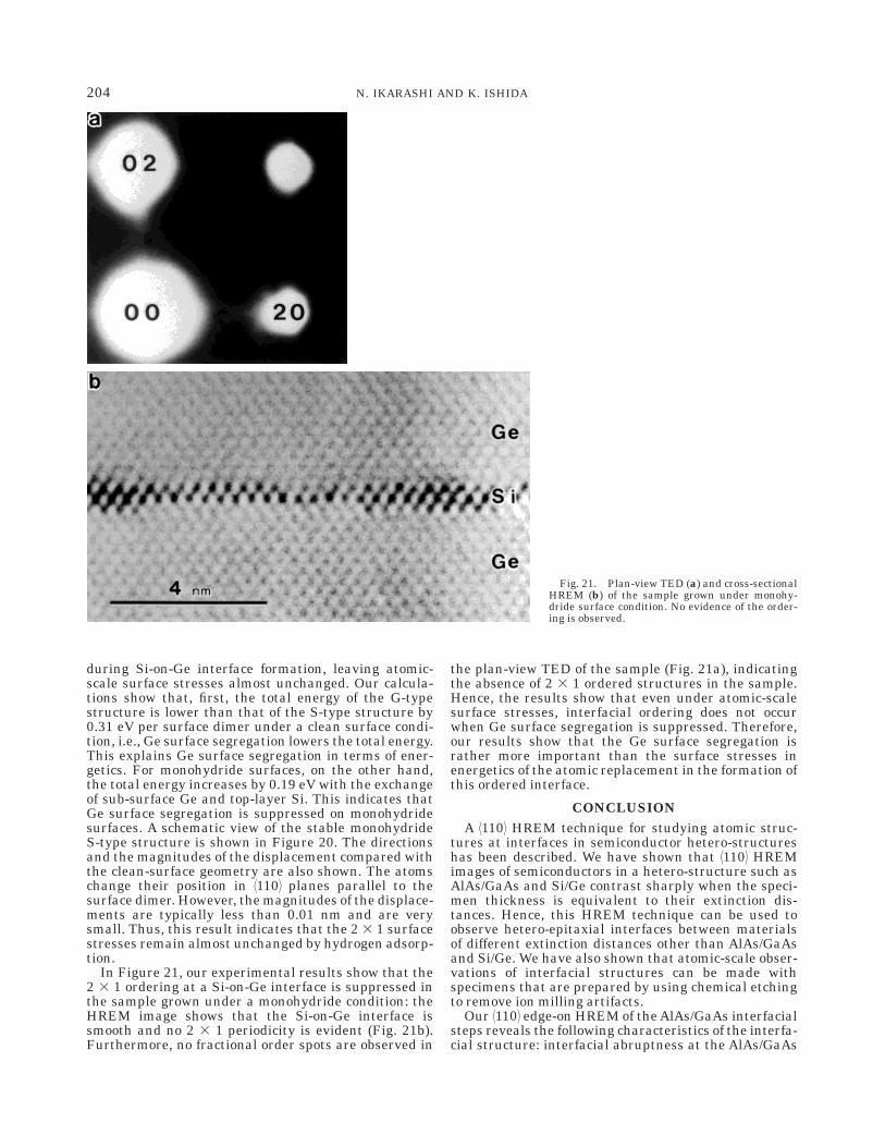
In Figure 21, our experimental results show that the2 3 1 ordering at a Si-on-Ge interface is suppressed inthe sample grown under a monohydride condition: theHREM image shows that the Si-on-Ge interface issmooth and no 2 3 1 periodicity is evident (Fig. 21b).Furthermore, no fractional order spots are observed in
the plan-view TED of the sample (Fig. 21a), indicatingthe absence of 2 3 1 ordered structures in the sample.Hence, the results show that even under atomic-scalesurface stresses, interfacial ordering does not occurwhen Ge surface segregation is suppressed. Therefore,our results show that the Ge surface segregation israther more important than the surface stresses inenergetics of the atomic replacement in the formation ofthis ordered interface.
CONCLUSIONA 71108 HREM technique for studying atomic struc-
tures at interfaces in semiconductor hetero-structureshas been described. We have shown that 71108 HREMimages of semiconductors in a hetero-structure such asAlAs/GaAs and Si/Ge contrast sharply when the speci-men thickness is equivalent to their extinction dis-tances. Hence, this HREM technique can be used toobserve hetero-epitaxial interfaces between materialsof different extinction distances other than AlAs/GaAsand Si/Ge. We have also shown that atomic-scale obser-vations of interfacial structures can be made withspecimens that are prepared by using chemical etchingto remove ion milling artifacts.
Our 71108 edge-on HREM of the AlAs/GaAs interfacialsteps reveals the following characteristics of the interfa-cial structure: interfacial abruptness at the AlAs/GaAs
Fig. 21. Plan-view TED (a) and cross-sectionalHREM (b) of the sample grown under monohy-dride surface condition. No evidence of the order-ing is observed.
204 N. IKARASHI AND K. ISHIDA
interface, differences in step edge straightness betweenA-steps and B-steps, and definite step interval distribu-tions at vicinal interfaces. Our 71108 HREM method hasalso shown the effects of growth interruption on inter-face smoothing. Hence, these observed interfacial struc-tures show that the growth surface structures prior tointerface formation are well maintained at the inter-face in AlAs/GaAs interfaces. In the study of Si/Geinterfacial structures, we have determined experimen-tally the chemically ordered 2 3 1 structure of an MBEgrown Si/Ge interface, and have investigated the ener-getics of the interfacial ordering using first-principlestotal-energy calculations. The results have shown thatGe surface segregation due to the chemical speciesdifference between Ge and Si and the stresses inherentto the 2 3 1 reconstruction at the growth surface playimportant roles in the ordering.
ACKNOWLEDGMENTSWe are pleased to thank Professor Hiroyuki Sakaki,
and Dr. Masaaki Tanaka of Tokyo University, ProfessorKoichi Akimoto of Nagoya University, Professor Atsu-shi Oshiyama of Tsukuba University, Dr. Toshio Baba,Dr. Toru Tatsumi, and Dr. Haruhiko Ono for theircollaboration. We also thank Takesi Noda of TokyoUniversity for assistance in MBE growth, Hideo Kawanofor valuable suggestions on chemical etching, andMakiko Oshida for technical assistance.
REFERENCESBourret, A., Renault, A., and Anstis, G.R. (1978/79) Dislocation core
imaging in metals and semiconductors. Chem. Scr., 14:207–212.Chew, N.G., and Cullis, A.G. (1987) The preparation of transmission
electron microscopy specimens from compound semiconductors byion milling. Ultramicroscopy, 23:175–198.
Cowley, J.M., and Moodie, A.F. (1957) The scattering of electrons byatoms and crystals, I. A new theoretical approach. Acta Crystallogr.,10:609–619.
De Jong, A.F., Bender, H., and Cone, W. (1987) Actual composition ofexperimental and simulated lattice images of the GaAs/AlAs inter-face. Ultramicroscopy 21, 373–378.
Desseaux, J., Renault, A., and Bourret, A. (1977) Multi-beam latticeimages from germanium oriented in (011). Philos. Mag. 35:357–372.
Fukunaga, T., Kobayashi, K.L.I., and Nakashima, H. (1985) Photolu-minescence from AlGaAs-GaAs single quantum wells with growthinterrupted hetero-interfaces grown by molecular beam epitaxy.Jpn. J. Appl. Phys. 24:L510–L512.
Gibson, J.M., and Treacy, M.M.J. (1984) The effect of elastic relaxationon the local structure of lattice modulated thin films. Ultramicros-copy 14:345–350.
Gibson, J.M., Hull, R., Bean, J.C., and Treacy, M.M.J. (1985) Elasticrelaxation in transmission electron microscopy of strained-layersuperlattices. Appl. Phys. Lett. 46:649–651.
Glaisher, R.W., Spargo, A.C.E., and Smith, D.J. (1989a) A theoreticalanalysis of HREM imaging for 71108 tetrahedral semiconductors.Ultramicroscopy 27:19–34.
Glaisher, R.W., Spargo, A.C.E., and Smith, D.J. (1989b) A systematicanalysis of HREM imaging of elemental semiconductors. Ultrami-croscopy 27:35–52.
Hirsch, P.B., Howie, A., Nicholson, R.B., Pashley, D.W., and Welan,M.J. (1965) Electron Microscopy of Thin Crystals. Butterworth,London, p. 100.
Ide, T., Yamashita, A., and Mizutani, T. (1992) Direct observations ofthe growth interruption effect for molecular beam epitaxy growth onGaAs(001) by scanning tunneling microscopy. Phys. Rev. B. 46:1905–1908.
Ikarashi, N., Tanaka, M., Baba, T., Sakaki, H., and Ishida, K. (1993)High-resolution transmission electron microscopy of AlAs/GaAs
interfacial structure in the 71108 projection. Jpn. J. Appl. Phys.32:2824–2831.
Ikarashi, N., Akimoto, K., Tatsumi, T., and Ishida, K. (1994) Orderedstructure at Si/Ge interfaces. Phys. Rev. Lett. 72:3198–3201.
Ikarashi, N., Oshiyama, A., Sakai, A., and Tatsumi, T. (1995) Role ofGe surface segregation in Si/Ge interfacial ordering: Interfaceformation on a monohydride surface. Phys. Rev. B. 51:14786–14789.
Ishizuka, K. (1985) Contrast transfer of crystal images in TEM.Ultramicroscopy 5:55–65.
Jesson, D.E., Pennycook, S.J., and Baribeau, J.-M. (1991) Directimaging of interfacial ordering in Ultrathin (SimGen)p superlat-tices. Phys. Rev. Lett., 66:750–753.
Kelires, P.C., and Tersoff, J., (1989) Equilibrium alloy properties bydirect simulation: Oscillatory segregation at the Si-Ge(001) 2 3 1surface. Phys. Rev. Lett. 63:1164–167.
Laval, J.Y., Delamarre, C., Dubon, A., Schiffmacher, G., Teste deSagey, G., Guenais, B., and Regreny, A. (1987) Atomic structure ofinterfaces in GaAs/AlGaAs superlattices. J. Physiol. (Paris) (Colloq.C5) 48:97–99.
LeGoues, F.K., Kesan, V.P., Iyer, S.S., Tersoff, J., and Tromp, R. (1990)Surface-stress-induced order in SiGe alloy films. Phys. Rev. Lett.64:2038–2041.
Maher, D.M., Fraser, H.L., Humphreys, C.J., Knoell, R.V., and Bean,J.C. (1987) Detection and measurement of local distortions in asemiconductor layered structure by convergent-beam electron diffrac-tion. Appl. Phys. Lett. 50:574–576.
Muller, E., Nissen, H.-U., Ospelt, M., and von Kanel, H. (1989)Chemical ordering and boundary structure in strained-layer Si-Gesuperlattices. Phys. Rev. Lett. 63:1819–1822.
Neave, J.H., Joyce, B.A., Dobson, P.J., and Norton, N. (1983) Dynamicsof film growth of GaAs by MBE from RHEED observations. Appl.Phys. A31:1–8.
Oshiyama, A. (1995) Structure of steps and appearances of 53116 facetson Si(001) surfaces. Phys. Rev. Lett. 74:130–133 (and referencestherein).
Ourmazd, A., Kim, Y., and Bode, M. Mater. (1990) Diffusion andinterdiffusion in multilayered semiconductor system. Res. Soc.Symp. Proc. 163:639–646.
Pashley, M.D., Haberern, K.W., and Gaines, J.M. (1991) Scanningtunneling microscopy comparison of GaAs(001) vicinal surfacesgrown by molecular beam epitaxy. Appl. Phys. Lett. 58:406–408.
Petroff, P.M. (1977) Transmission electron microscopy of interfaces inIII-V compound semiconductors. J. Vac. Sci. Technol. 14:973–978.
Petroff, P.M., Gossard, A.C., Weigmann, W., and Savage, A. (1978)Crystal growth kinetics in (GaAs)m-(AlAs)n superlattices depositedby molecular beam epitaxy. J. Cryst. Growth 44:5–13.
Poudoulec, A., Guenais, B., D’anterroches, C., and Regreny, A. (1990)Interface structure of a GaAs-AlAs superlattice MBE grown on aGaAs vicinal surface. J. Cryst. Growth 100:529–538.
Pukite, P.R., Petrich, G.S., Batra, S., and Choen, P.I. (1989) Themeandering of steps on GaAs(001). J. Cryst. Growth 95:269–272.
Sakaki, H., Tanaka, M., and Yoshino, J. (1985) One atomic layerheterointerface fluctuations in GaAs/AlAs quantum well structuresand their suppression by insertion of smoothing period in molecularbeam epitaxy. Jpn. J. Appl. Phys. 24:L417–L420.
Sakaki, H., Noda, T., Tanaka, M., Motohisa, J., Kadoya, Y., Ikarashi,N. (1993) Atomic scale understanding and controllability of heteroin-terfaces in quantum microstructure. In: Semiconductor Interfacesat the Sub-Nanometer Scale. H.W.M. Salemink, ed. (NATO/ASIseries E.), vol. 243, pp. 217–230.
Stenkamp, D., and Jager, W. (1993) Compositional and structuralcharacterization of SiGe alloys and heterostructures by high-resolution transmission electron microscopy. Ultramicroscopy 50:321–354.
Takayangi, K., Tanishiro, Y., Takahashi, S., and Takahashi, M. (1985)Structure analysis of Si(111) 7 3 7 reconstructed surface by transmis-sion electron diffraction. Surf. Sci. 164:367–392.
Tanaka, M., and Sakaki, H. (1987) Atomic models of interface struc-tures of GaAs-AlGaAs grown by interrupted and uninterruptedMBE. J. Cryst. Growth 81:153–158.
Tanaka, M., Sakaki, H., and Yoshino, J. (1986) Atomic-scale structuresof top and bottom heterointerfaces in GaAs-AlGaAs quantum wellsprepared by molecular beam epitaxy with growth interruption. Jpn.J. Appl. Phys. 25:L155–L158.
205,110. HREM METHOD