Embed Size (px)
Citation preview

Welcome to the 10th East Asia Symposium on
Superconductor Electronics
Dear colleagues and friends,
It is our great honor and pleasure to organize the 10th East Asia Symposium on
Superconductor Electronics (EASSE-2019), which will be held in Beijing, China
from Oct. 8 to Oct. 11, 2019. Following the tradition of this series, the coming
symposium will bring together the researchers on superconductor electronics
across East Asia to exchange and share our research ideas and results, as well as
to meet old friends and make new friends, so that we shall further strengthen the
collaboration between us and promote the research and applications of
superconductor electronics in East Asia.
Not only the capital of China but also a city vibrant with life and energy, Beijing
has many new things to offer, even to frequent visitors, in addition to its numerous
historical scenic spots. And October is the best time in a year to see it as well as
the other parts of China.
Do come to EASSE-2019. We shall do our best to make your participation fruitful
and rewarding, both professionally and socially.
B.S. Cao,Symposium Chair

Sponsors
Tsinghua University
Nanjing University
Western Superconducting Technologies Co.,Ltd.
Chinese Institue of Electronis
National Natural Science Foundation of China
Ministry of Science and Technology of the People’s Republic of China
Ministry of Education of the People’s Republic of China

The 10th East Asia Symposium on Superconductor
Electronics (EASSE-2019)
International Steering Committee
S. Ohshima ( Yamagata University, Yonezawa ), Chairman
B.S. Cao ( Tsinghua University, Beijing )
J. Chen ( Nanjing University, Nanjing )
H.E. Horng ( National Taiwan Normal University, Taipei )
N. Khare ( Indian Institute of Technology, Delhi )
H.J. Lee ( Pohang University of Science and Technology, Pohang )
Y.H. Lee (KRISS, Daejeon )
K. Nakajima (Yamagata University, Yonezawa)
Y.K. Park ( University of Science and Technology, Daejeon )
K. Tanabe ( ISTEC, Tokyo )
T. Venkatesan ( National University of Singapore, Xiamen University Malaysia )
L.M. Wang ( National Taiwan University, Taipei )
P.H. Wu ( Nanjing University, Nanjing )
International Advisory Committee
Z.G. Khim( Seoul National University, Seoul )
S. Kuriki( Hokkaido University, Sapporo )
C.K. Ong( National University of Singapore, Xiamen University Malaysia)
Organizing Committee
B.S. Cao ( Tsinghua University, Beijing ), Chairman
Y.R. Li ( Sichuan University, Chengdu ), Co-Chairman
J. Chen ( Nanjing University, Nanjing ), Co-Chairman
B. Wei ( Tsinghua University, Beijing ), Co-Chairman
D.K. Chen ( CETC, Hefei )
J. Li ( IOP, CAS, Beijing )
Y.P. Liu ( IOP, CAS, Beijing )
L.X. You ( SIMIT, CAS, Shanghai )
F.R. Wang ( Peking University, Beijing )
D.N. Zheng ( IOP, CAS, Beijing )
Topics
1) Materials and Device Fabrication;
2) RF Components and Devices;
3) SQUIDs and Applications;
4) Detectors and Applications;
5) Digital;
6) Quantum Information;
7) Cryogenic and Electrical Systems;
8) Novel Devices;
9) Metrology and Standard;
10) Topological Devices.


Conference Venue: Unisplendour International Center (October 9th 8:30 - 11:40)
Conference Venue: Jinchunyuan (October 9th 14:00 - 21:00, October 10th, October 11th)

EASSE 2019 – Program Tuesday 8 October, 2019
14:00 18:00 Registration (Location: Jinchunyuan)
18:00 20:00 Reception (Location: Jinchunyuan restaurant)
Wednesday 9 October, 2019 Conference Venue: Unisplendour International Center (October 9th 8:30 - 11:40)
Opening ceremony (Chair: Jian Chen)
8:30 8:40 Welcome address by professor Qikun Xue, vice president of Tsinghua University
8:40 8:50 Opening address by professor Peiheng Wu, Nanjing University
8:50 9:00 Welcome by professor Bisong Cao, Tsinghua University
9:00 9:30 Group photo of EASSE2019 & Coffee break
9:30 10:00 Memorial to Prof. Tsutomu Yamashita
Session I (Chairs: Yang Yu, Akira Fujimaki) Superconducting Computing & Circuits
10:00 10:20 Akira Fujimaki Numerical and Experimental Analysis on π-Shifted
SQUIDs for Logic Circuits and Memories Page 1
10:20 10:40 Mutsuo Hidaka Improvements of superconducting digital circuit
fabrication process Page 2
10:40 11:00 Kai Xu Generation of multicomponent atomic Schrödinger
cat states of up to 20 qubits Page 3
11:00 11:20 Yang Yu Simulation and manipulation of topological bands
using superconducting quantum circuits Page 4
11:20 11:40 Zhirong Lin Real-time detection of an itinerant microwave
photon using dressed-state engineering Page 5
12:00 13:00 Lunch (Location: Jinchunyuan restaurant)
Conference Venue: Jinchunyuan (October 9th 14:00 - 21:00, October 10th, October 11th)
Session II (Chairs: Huabing Wang, Masayoshi Tonouchi) Meeting Room 3 Microwave
14:00 14:20 Lu Ji Growth and properties analysis on epitaxial 2 inch
Tl-2212 superconducting films Page 6
14:20 14:40 Haiwen Liu
Compact and High Performance Microwave
Superconducting Bandpass Filters Using Microstrip
Multimode Resonators
Page 7
14:40 15:00 Liang Sun Development of the Ultra-wideband HTS Microstrip
Filters Page 8
15:00 15:20 Ming-Jye Wang Toward Full RF-Bandwidth mm-Wavelength
Receiver for Astronomical Telescope Page 9
15:20 15:40 Sansheng Wang
High quality uniform REBCO film growth by the
metalorganic deposition using trifluoroacetates and
its modifications for large-power microwave
devices application
Page 9
15:40 16:00 Xuehui Guan Novel Spiraled D-CRLH High Temperature
Superconducting Filter with a Dual-Passband Page 11
16:00 16:20 Coffee break
Session III (Chairs: Hideo Itozaki, Jinjin Li) Meeting Room 2 SQUIDs
14:00 14:20 Saburo Tanaka
Development of High-Tc SQUID Metallic
Contaminant Detection System for Li-ion Battery
Components
Page 12
14:20 14:40 Xiaoming Xie SQUID Systems for Bio-imaging/testing and
Geophysical Prospection Page 13
14:40 15:00 Jen-Jie Chieh Nonn-invasive and Fast Imaging Tumors by SQUID Page 14

16:00 16:20 Coffee break
Session IV (Chairs: Haiwen Liu,Ming-Jye Wang) Meeting Room 3 Junctions
16:20 16:40 Huabing Wang Josephson junctions with novel barrier layers Page 18
16:40 17:00 Hu-Jong Lee Strong proximity Josephson coupling in
heterojunctions of 2D materials Page 19
17:00 17:20 Akinobu Irie Spin-dependent behaviors in Ferromagnet/Intrinsic
Josephson junctions/Ferromagnet Hybrids Page 20
17:20 17:40 Masayoshi Tonouchi Ultrafast optical response and vortex generation in
high-Tc superconductors Page 21
18:00 19:00 Dinner (Location: Jinchunyuan restaurant)
Session V (Chair: Masataka Ohkubo) Meeting Room 2 Standard
16:20 16:40 SangYoung Lee
Two-resonance-mode dielectric resonator method
as an International Standard for the Intrinsic Surface
Impedance of High-Tc Superconductor Films
Page 22
16:40 17:00 Jinjin Li
The Development of Large-scale Josephson
Junction Array Devices for the Quantum Voltage
Standard at NIM
Page 23
17:00 17:20 Myung-Ho Bae Quantum metrology triangle for future electrical
standard Page 24
18:00 19:00 Dinner (Location: Jinchunyuan restaurant)
Biosusceptometry and Magnetic Nanoparticles
15:00 15:20 Shu-Hsien Liao High-Tc SQUID based NMR for breast cancer and
liver cancer diagnosis Page 15
15:20 15:40 Kenji Sakai Estimation of electrochemical impedance using
HTS-SQUID based magnetic measurement system Page 16
15:40 16:00 Li-Min Wang
Characterization of High-Tc dc-SQUID
Magnetometers: Fabrication with Sputtered YBCO
Films Deposited on Recycled SrTiO3 Bi-crystal
Substrates
Page 17

Poster Session (Chairs: Dongning Zheng, Takashi Tachiki) Meeting Room 3
19:00 21:00
Hirofumi Yamasaki
Correlation between the critical current density and
surface resistance in YBCO thin films—
reexamined
Page 46
Fang Li
Vortex manipulation with dots and antidots on
superconductivity of REBa2Cu3O7-δ films growth
by trifluoroacetate metal organic deposition method
Page 47
Xiaoqing Sun Effects of Ionic Accumulation in Nerve Conduction Page 48
Teppei Ueda Property of HTS Josephson Junction irradiated by
Ga Focused Ion Beam Page 49
Guofeng Zhang LTS SQUID magnetometers and gradiometers Page 50
Yifeng Pei LTS SQUID Based Transient Electromagnetic
System for Geophysical Prospecting Page 51
Yingyi Shao Control of roughness and stress of Nb films for
Nb/Al‐AlOx/Nb Josephson junctions Page 52
Zuyu Xu Tunable Josephson junction based on black
phosphorus Page 53
Shixian Chen Novel Nb-based Josephson junctions using
Bi2Sr2CaCu2O8+δ as barriers Page 54
Fajun Li Proximity Effects on Mo/Cu Bilayers Page 55
Sifan Wang Development of Mo/Cu TES Devices Page 56
Yeru Wang Characterization of Sputtered Molybdenum Thin
Films Page 57
Takahiro Murakami Bi-2212 mesas made of Bi-2212 thin film for THz
emission with superior heat dissipation. Page 58
Zaidong Qi High-power terahertz emission from
Bi2Sr2CaCu2O8 intrinsic Josephson junction stacks Page 59
Runfeng Su Characterization of superconducting NbN hot-
electron bolometers as THz direct detectors Page 60
Herng-Er Horng The application of high-Tc SQUID-based low-field
NMR in human liver tumor discrimination Page 61
Steering Committee (Chair: Shigetoshi Ohshima) Meeting Room 2
18:00 19:00 Steering Committee

Thursday 10 October,2019 Session VI (Chairs: Yoshihiko Takano, Akinobu Irie) Meeting Room 3 THz
8:40 9:00 Takashi Tachiki
Investigation of radiation properties of THz-wave
oscillators using Bi-2212 intrinsic Josephson
junctions for oscillator-array design
Page 25
9:00 9:20 Akira Kawakami 2 THz Hot Electron Bolometer Mixer using a
Magnetic Thin Film Page 26
9:20 9:40 Hsiao-Wen Chang Development of NbN Hot Electron Bolometer
Mixer Operating at 1.5 THz Page 27
9:40 10:00 Kensuke Nakajima Applications of superconducting thin films for
extensive use in terahertz functional devices. Page 28
10:00 10:20 Nobuyuki Yoshikawa Extremely Energy-Efficient Circuit Technology
based on Adiabatic Quantum Flux Parametron Page 29
10:20 10:40 Coffee break
Standardization Session (Chairs: SangYoung Lee, Masataka Ohkubo) Meeting Room 2
8:40 10:20 Shigetoshi Ohshima TC90/WG8&WG14 Page 30
10:20 10:40 Coffee break
Session VII (Chair: Kensuke Nakajima) Meeting Room 3 Others
10:40 11:00 Yoshihiko TAKANO Discovery of new superconductors under high
pressure using materials informatics Page 31
11:00 11:20 Hideki Ichinose Specimen Thinning for HRTEM via Photon
illumination Page 32
11:20 11:40 Chong Kim Ong Electrical signal transmission in Neural Functions Page 33
12:00 13:00 Lunch (Location: Jinchunyuan restaurant)
Session VIII (Chair: Nobuyuki Yoshikawa) Meeting Room 2 SNSPD
10:40 11:00 Lixing You Superconducting nanowire single photon
detectors for quantum information Page 34
11:00 11:20 Hirotaka Terai Recent progress in research and development of
superconducting nanowire single-photon detectors Page 35
11:20 11:40 Labao Zhang The original seeds of dark counts of SNSPD Page 36
12:00 13:00 Lunch (Location: Jinchunyuan restaurant)
13:00 18:00 Lab tour
18:00 21:30 Conference Banquet (Location: Laoshe Teahouse)

Friday 11 October,2019 Session IX (Chairs: Lixing You, Hirotaka Terai) Meeting Room 3 TES
8:40 9:00 Wei Cui Superconducting Detectors and Electronics for
Astronomical Applications Page 36
9:00 9:20 Yong Hamb Kim Metallic magnetic calorimeters for astroparticle
physics applications Page 38
9:20 9:40 Shuo Zhang Introduction to cryogenic particle detectors for
Shanghai Light source Facility Page 39
9:40 10:00 Takekazu Ishida Neutron imaging using a superconducting detector Page 40
10:00 10:20 Masataka Ohkubo
A challenge to chemical-state nanoscale-imaging
with superconductor-tunnel-junction X-ray detector
for aviation industry
Page 42
10:20 10:40 Coffee break
Session X (Chair:Hu-Jong Lee) Meeting Room 3 SQUIDs
10:40 11:00 Hideo Itozaki High Tc Scanning SQUID Microscope Page 44
11:00 11:20 Anjan Kumar Gupta Optimization of constriction based Nb µ-SQUIDs
for probing nano-magnetism Page 45
11:20 11:40 Neeraj Khare
11:40 12:00 Shigetoshi Ohshima Closing Remarks
12:00 13:00 Lunch (Location: Jinchunyuan restaurant)

Abstract Book

1
Numerical and Experimental Analysis on -Shifted
SQUIDs for Logic Circuits and Memories
A. Fujimaki1, Y. Takeshita1, D. Hasegawa1, F. Li1, K. Sano1,
M. Tanaka1, and T. Yamashita1,2
1Department of Electronics, Nagoya University, Nagoya.
2JST-PRESTO
We have successfully demonstrated -shifted SQUIDs (-SQUIDs) made up of two
conventional Nb/AlOx/Nb Josephson junctions and a single -shifted magnetic Josephson
junctions (hereinafter junctions). The junctions have a sandwich structure of a Nb/PdNi/Nb
trilayer. We confirm that modulation patterns of the critical currents to external magnetic fields
in -SQUIDs are shifted by a field corresponding to half of magnetic flux quantum as shown
in Figure 1.
The -SQUIDs function as an essential element of the half flux quantum (HFQ) logic circuit.
Figure 1 indicates that the -SQUIDs can be regarded as single junctions with reduced critical
currents. In addition, the phase change in a single switching of -SQUIDs is , so that HFQ
logic circuits can be built up by replacing conventional single junctions of the rapid single flux
quantum (RSFQ) circuits with -SQUIDs [1]. Numerical analysis of the HFQ circuits made
up of 100-A-junctions shows that the energy consumption is reduced below 0.05 aJ/junction,
which is 1-2 orders of magnitude smaller than that of the RSFQ circuit.
The -SQUIDs have two stable states corresponding to a clockwise and counter-clockwise
circulating current without any field. The potential barrier height between the two states can be
controlled by adjusting a loop inductance of the -SQUID or a critical current of an inserted
additional junction. The low barrier height enables us to make a large capacity matrix memory
driven by an impulse like an SFQ pulse [2].
The detail of the numerical and experimental analysis will be given at the symposium.
Fig. 1 Experimentally obtained modulation pattern of critical current of a -SQUID
[1] T. Kamiya, et al., IEICE Trans. Electron. E101-C (2018) 385.
[2] Fujimaki, et al., 17th Int. Supercond. Electron. Conf., 2019, Riverside, CA, USA.
-15 -10 -5 0 5 10 15
0.20
0.15
0.10
0.05
0
-0.05
-0.10
-0.15
-0.20
Critic
al
cu
rren
t [m
A]
Applied magnetic flux density [µT]

2
Improvements of superconducting digital circuit
fabrication process
M. Hidaka1
1National Institute of advanced industrial science and technologies (AIST), Tsukuba.
Superconducting digital circuits are attractive for their high-speed and low-dissipation
characteristics. AIST is routinely fabricating Nb-based superconducting digital circuits and also
investigating advanced fabrication process toward higher performances and various
applications. For examples, 106 GHz clock operation of a single-flux-quantum (SFQ) processor
was demonstrated using Josephson junctions (JJs) of 20 kA/cm2 critical current density (Jc)
[1], circuits area of adiabatic quantum flux parametron (AQFP) were reduced 40% by a
double gate layer device structure [2] and outputs of superconducting strip photon detectors
(SSPD) were effectively combined by a monolithic SFQ readout circuit [3]. We found out main
origin of SFQ circuit defects was small particles underneath JJs. Replacement of deposition
method of SiO2 from bias sputter to chemical vapor deposition (CVD) which generates much
fewer particles than that by bias sputter achieved dramatically improvement of SFQ circuit
integration level [4].We are also developing quantum annealing circuits based on the digital
fabrication process with Jc of 0.1 kA/cm2 which is 100 times smaller compared with ordinary
digital circuits [5].
A part of his presentation is based on results obtained from a project commissioned by the New
Energy and Industrial Technology Development Organization (NEDO) and JSPS-KAKENHI
18H05211, 18H05245.
[1] M. Tanaka, M. Kozaka, Y. Kita, A. Fujimaki, S. Nagasawa, and M. Hidaka (2015). IEEE Trans. Appl.
Supercond., Vol. 25, pp. 1–4.
[2] T. Ando, S. Nagasawa, N. Takeuchi, N. Tsuji, F. China, M. Hidaka, Y. Yamanashi, and N. Yoshikawa, (2017).
Supercond. Sci. Technol., Vol. 30, 075003.
[3] H. Terai, S. Nagasawa, S. Miyajima, T. Yamashita, S. Miki, M. Yabuno, and M. Hidaka (2016). ASC2016,
3EOr1B-03
[4] M. Hidaka, S. Nagasawa, T. Satoh and K. Hinode (2015). ,IEEE Xplore, 10.1109/ISEC2015.
[5] M. Maezawa, G. Fujii, M. Hidaka, K. Imafuku, K. Kikuchi, H. Koike, K. Makise, S. Nagasawa, H. Nakagawa,
M. Ukibe, and S. Kawabata (2019). J. Phys. Soc. Jpn., 061012.
3
Generation of multicomponent atomic Schrödinger
cat states of up to 20 qubits
Chao Song1†, Kai Xu2†, Hekang Li2†, Yu-Ran Zhang2,5, Xu Zhang1,
Wuxin Liu1, Qiujiang Guo1, Zhen Wang1, Wenhui Ren1, Jie Hao3,
Hui Feng3, Heng Fan2*, Dongning Zheng2*, Da-Wei Wang1,
H. Wang1*, Shi-Yao Zhu1
1Department of Physics, Zhejiang University, Hangzhou.
2Institute of Physics, Chinese Academy of Sciences, Beijing.
3Institute of Automation, Chinese Academy of Sciences, Beijing.
5Beijing Computational Science Research Center, Beijing.
*Corresponding author. E-mail: [email protected] (H.F.); [email protected] (D.N.Z.);
[email protected] (H.W.).
†These authors contributed equally to this work.
Multipartite entangled states, especially the Greenberger-Horne-Zeilinger (GHZ) states, are a
fundamental resource for numerous applications in quantum information science, but the
generation of such states remains an outstanding challenge due to their intrinsic fragilities.
Therefore, the creation of multiqubit GHZ states serves as an important benchmark for
characterizing the controllability and scalability of experimental quantum platforms [1,2]. We
report the deterministic generation of an 18-qubit GHZ state and multicomponent atomic
Schrödinger cat states of up to 20 qubits on a quantum processor, which features 20
superconducting qubits, also referred to as artificial atoms, interconnected by a bus resonator.
By engineering a one-axis twisting Hamiltonian, the system of qubits, once initialized,
coherently evolves to multicomponent atomic Schrödinger cat states—that is, superpositions of
atomic coherent states including the GHZ state—at specific time intervals as expected. We
measure a GHZ state fidelity F = 0.525 ± 0.005 for 18 qubits, confirming genuine 18-partite
entanglement. Our approach on a solid-state platform should not only stimulate interest in
exploring the fundamental physics of quantum many-body systems, but also enable the
development of applications in practical quantum metrology and quantum information
processing.
[1] Omran et al., Generation and manipulation of Schrödinger cat states in Rydberg atom arrays. Science 365,
570-574 (2019).
[2] K. X. Wei et al., Verifying multipartite entangled GHZ states via multiple quantum coherences.
arXiv:1905.05720 [quant-ph].

4
Simulation and manipulation of topological bands
using superconducting quantum circuits
Xinsheng Tan1, Yuxin Zhao1,2, Danwei Zhang3, Mengmeng Li1, Haifeng Yu1, Hui Yan3,
Shiliang Zhu1,3, Yang Yu1, Zidan Wang2,
1National Laboratory of Solid State Microstructures, School of Physics, Nanjing University,
China 2Department of Physics, The University of Hong Kong
3Guangdong Provincial Key Laboratory of Quantum Engineering and Quantum Materials,
SPTE, South China Normal University, Guangzhou 510006, China
Topological band theory has attracted much attention since several types of topological metals
and semimetals have been explored. These robustness of nodal band structures are symmetry-
protected, whose topological features have deepened and widened the understandings of
condensed matter physics. Meanwhile, as artificial quantum systems superconducting circuits
possess high controllability, supplying a powerful approach to investigate topological
properties of condensed matter systems. We realize Hamiltonians with topological symmetry
by mapping momentum space to parameter space in a superconducting quantum circuit[1-4].
By measuring energy spectrum of the system, we observe the gapless band structure of
topological semimetals, shown as Dirac points or Weyl points in momentum space. The phase
transition from topological semimetal to topological insulator can be realized by continuously
tuning the parameter in Hamiltonian. Our work open a platform to simulate the relation between
the symmetry and topological stability in condensed matter systems.
[1] Xinsheng Tan, Yuxin Zhao, Qiang Liu, Guangming Xue, Haifeng Yu, Z. D. Wang, Yang Yu, Npj Quantum
Materials 2, 60 (2017).
[2] Xinsheng Tan, Dan-Wei Zhang, Qiang Liu, Guangming Xue, Hai-Feng Yu, Yan-Qing Zhu, Hui Yan, Shi-
Liang Zhu, Yang Yu, Phys. Rev. Lett. 120, 130503 (2018).
[3] Xinsheng Tan, Mengmeng Li, Danyu Li, Kunzhe Dai, Haifeng Yu, Yang Yu, Appl. Phys. Lett. 112, 172601
(2018).
[4] Xinsheng Tan, Yuxin Zhao, Qiang Liu, Guangming Xue, Haifeng Yu, Zidan Wang, Yang Yu, Phys. Rev.
Lett. 122, 010501 (2019).

5
Real-time detection of an itinerant microwave
photon using dressed-state engineering
Zhirong Lin1,2
1CAS Center for Excellence in Superconducting Electronics, Shanghai Institute of
Microsystem and Information Technology, Shanghai, China
2 Center for Emergent Matter Science, RIKEN, Wako, Japan
Several schemes for single microwave photon detection have been proposed and demonstrated
lately in circuit quantum electrodynamics [1-4]. However, most experimental demonstration to
date are performed in the time-gated mode. In this presentation, we demonstrate a real-time
detection of itinerant microwave photons. In our setup, a superconducting flux qubit is coupled
to two resonators, which have substantial difference in the dispersive shifts. Under an adequate
choice of the frequency and the power of the qubit drive, one resonator is used to form an
impedance-matched Λ system that deterministically captures incoming photons, and the other
is used for continuous monitoring of the event. We observe a quantum jump produced by an
itinerant microwave photon and attain a single-photon-detection efficiency of ~0.35. The
detection efficiency of this detector is limited by the relatively short qubit relaxation time.
[1] K. Inomata*, Z. R. Lin*, et al. (2016). Single microwave-photon detector using an artificial Λ-type three-
level system. Nature Commun., 7, 12303.
[2] S. Kono et al. (2018). Quantum non-demolition detection of an itinerant microwave photon. Nature Physics,
14, 546.
[3] Jean-Claude Besse et al. (2018). Single-Shot Quantum Nondemolition Detection of Individual Itinerant
Microwave Photons. Phys. Rev. X, 8, 021003.
[4] Raphaël Lescanne et al. (2019). Detecting itinerant microwave photons with engineered non-linear
dissipation. arXiv:1902.05102

6
Growth and properties analysis on epitaxial 2 inch
Tl-2212 superconducting films
X. L. Liang, J. Xin, T. Xue, M. He, S. L. Yan, and L. Ji
School of Electronic Information and Optical Engineering, Nankai University, Tianjin.
The extensive use of large-area high temperature superconducting (HTS) thin films has
emerged in superconducting microwave devices. The interest in the Tl-based HTS films arises
from their higher critical temperature (Tc), which avoids the demands for more cryogenic device.
This paper introduces a developed two-step method without additional Tl source to fabricate
high-quality Tl2Ba2CaCu2O8 (Tl-2212) films on 2 inch LaAlO3 substrates. This method enables
the preparation of Tl-2212 films to be less complicated and more repeatable, which can promote
the theoretical research and practical application of Tl-based films. Based on the high
reproducibility of this fabricating process, the obtained 2 inch Tl-2212 films have excellent
quality, the superconducting properties of Tc, the critical current density Jc (77K, zero field) and
surface resistance (Rs) of 2 inch samples can be studied easily. The Tc value of sample films
prepared at different conditions varies from 99 to 103 K, and Jc of films ranges from 0.7 to
1.8MA/cm2. Systematic experiment reveals that the oxygen content affects the Tc of the films,
and the surface roughness of the films is closely related to Jc values. The variation of Rs
(calculated at 12GHz) with temperatures on Tl-2212 films was also observed, which is a helpful
guideline for the application of microwave devices based on Tl-2212 films.

7
Compact and High Performance Microwave
Superconducting Bandpass Filters Using Microstrip
Multimode Resonators
Haiwen Liu
School of Electronics and Information Engineering, Xi'an Jiaotong University, Xi'an
As the key passive component in the radio-frequency (RF) front-end, bandpass filter (BPF) with
compact size and high performance are in great demand for enhancing system functionality. Meanwhile,
high-temperature superconducting (HTS) materials are becoming more and more attractive in the
context of designing microwave filters because of their lower losses and excellent performance.
In past few years, several types of high performance HTS BPFs have been designed for demonstration.
For circuit size miniaturization, various microstrip multimode resonators have been proposed, such as
the multi-stub-loaded resonators and square ring loaded resonator. At first, a series of the second-order
multiband HTS filters have been presented based on the multi-stub-loaded resonators [1], [2]. The
measured insertion losses are all extremely small, but the selectivity and stopband performance need to
be improved because of the low-order design. Therefore, a newly dual-mode hairpin ring resonator is
proposed and applied to constitute an eighth-order dual-band HTS BPF [3]. The configuration of the
designed filter and the obtained frequency responses are respective shown in Fig. (a) and (b). As
predicted, the band edge selectivity and the attenuation in stopband are highly enhanced.
In addition, the differential circuits have been received much attention recently due to their ability of
lower electromagnetic noise and crosstalk. So, based on the HTS technology, a fourth-order differential
dual-band HTS BPF has been designed using the proposed square ring loaded resonator [4]. The layout
of the differential filter is depicted in Fig. (c) and the simulated results as well as the measured results
are shown in Fig. (d). It is seen from Fig. (d) that a favorable common-mode (interference signal)
suppression over a wide frequency range is obtained.
With the advantages of ultra-low in-band insertion losses and high selectivity, these proposed filters are
attractive for potential applications in multiband communication systems requiring high-sensitivity and
high anti-interference properties.
[1] H. W. Liu, J. H. Lei, X. H. Guan, L. Sun, and Y. S. He, “Compact triple-band high-temperature
superconducting filter using multimode stub-loaded resonator for ISM, WiMAX, and WLAN Applications,”
IEEE Transactions on Applied Superconductivity, vol. 23, no. 6, Art. ID. 1502406, Dec. 2013.
[2] H. W. Liu, P. Wen, Y. L. Zhao, B. P. Ren, X. M. Wang, and X. H. Guan, “Dual-band superconducting
bandpass filter using quadruple-mode resonator,” IEEE Transactions on Applied Superconductivity, vol. 24,
no. 2, pp. 130-133, Apr. 2014.
[3] H. W. Liu, B. P. Ren, S. X. Hu, X. H. Guan, P. Wen, and J. M. Tang, “High-order dual-band superconducting
bandpass filter with controllable bandwidths and multitransmission zeros,” IEEE Trans. Microw. Theory
Tech., vol. 65, no. 10, pp.3813-3823, Nov. 2017.
[4] B. P. Ren, Z. W. Ma, H. W. Liu, X. H. Guan, X. L. Wang, P. Wen, and M. Ohira, “Differential Dual-Band
Superconducting Bandpass Filter Using Multi-Mode Square Ring Loaded Resonators With Controllable
Bandwidths,” IEEE Transactions on Microwave Theory and Techniques, vol. 67, no. 2, pp. 726-737, Feb.
2019.

8
Development of the Ultra-wideband HTS Microstrip
Filters
Y. Wu1, L. Sun1, C. Li1, X. Zhang1, J. Wang1, X. Wang1, Y. Bian1, G. Li1, H. Li1, and Y. He1
1 Beijing National Laboratory of Condensed Matter Physics and Institute of Physics, Chinese
Academy of Sciences
Ultra-wideband (UWB) technology is been known as with advantages such as high
communication speed, low power consumption and high anti-jamming performance. It has been
widely used in radio astronomy observation, deep space exploration and wireless
communication. As a key unit in front-end of RF receivers, UWB filters have been developed
massively. In this talk, UWB filters developed on high temperature superconducting microstrip
lines are presented. Firstly, a wideband filter for radio astronomy observation, which has a
fractional bandwidth (FBW) of 37.8%, is introduced. By adopting a hairpin-like structure,
resonators can generate strong coupling, and push its first spurious resonant peak away from
the passband. Then, a UWB filter for deep space exploration, which has an FBW of 65%, is
presented. λ/4 hair-pin resonators were used in this filter instead of regular /2 resonators,
which not only minimized the size of the filter, but also eliminated the effect of second
harmonic resonance of /2 resonators. Finally, a filter with an FBW of 108% for wireless
communication is introduced. The filter is realized by cascading a high-pass filter and a low-
pass filter, with a low noise amplifier inserted between the high-pass filter and the low-pass
filter to improve the matching between the filters.

9
Toward Full RF-Bandwidth mm-Wavelength
Receiver for Astronomical Telescope
M. J. Wang1*, T. J. Chen1, W. C. Lu1, Y. B. Chang1, Y. D. Huang1, C. E. Tong2, L. Zeng2, P.
Grime2
1Institute of Astronomy and Astrophysics, Academia Sinica, Taipei, Taiwan
2Harvard-Smithsonian Center for Astrophysics, Cambridge, MA 02138, USA
The construction and operation of cutting-edge astronomical telescope is very expensive.
Improving the sensitivity and efficiency is an important issue for detecting system development.
For radio telescope receiver, the simultaneous observation bandwidth is the key parameter. For
total power detection mode, the sensitivity is proportional to 1 √𝐵𝑊⁄ , i.e. wider bandwidth
resulting in higher sensitivity. For the spectrum detection mode, the wider bandwidth can
observe more emission lines in one integration and speed up the observation.
In a mm-wavelength receiver, the RF signal coupled through feed horn can be up to 100GHz.
However, the observation bandwidth is dependent on the intermediate frequency (IF)
bandwidth of receiver with single tone local oscillator (LO) source in the regular system
configuration. Cooled low noise amplifier (CLNA) and superconductor-insulator-
superconductor (SIS) mixer are the two critical components. After years effort, the wSMA
receiver has demonstrated the-state-of-art ultrawide bandwidth of 32 GHz [1]. Further
extending the bandwidth of CLAN and SIS mixer becomes difficult due to the impendence
match issue.
A possible approach to extend the simultaneous observation bandwidth further is using multi-
receivers pumped at different LO frequencies. The RF signal is divided into several sub-bands
by superconducting bandpass filters. The individual sub-band RF signal is detected by an SIS
mixer which is pumped by the LO source at the center frequency of sub-band. The observation
bandwidth of this detection scheme could be increased by a factor of the number of sub-bands.
In my presentation, I will include the detail scheme of full RF-bandwidth receiver, the
developed ultrawide wSMA receiver, and some preliminary works on bandpass filter in mm-
wavelength.
[1] C. Edward Tong, et. al. “Development of SIS Receivers with Ultra-wide Instantaneous Bandwidth for
wSMA”, 29th IEEE International Symposium on Space THz Technology (ISSTT2018), Pasadena, CA, USA,
March 26-28, 2018
High quality uniform REBCO film growth by the
metalorganic deposition using trifluoroacetates and

10
its modifications for large-power microwave devices
application
S.S.Wang1,3*, Z.L.Zhang1, F. Li1,B. Wei2, B.S.Cao2,L.K.Gao3,J.Liu3
1. Key Laboratory of Micro-nano Measurement, Manipulation and Physics (Beihang
University), Ministry of Education, Beijing 100191, China
2. Department of Physics, Tsinghua University, Beijing 100084, China
3.Beijing Dingchen Superconducting Technology Co., Ltd.
E-MAIL: [email protected]
A need exists for the large-area superconducting REBa2Cu3O7-x (REBCO) films with high
critical current density for microwave communication. Trifluoroacetic metalorganic (TFA-
MOD) method is a promising low cost technique for large-scale production of REBCO films,
because it does not need high vacuum device and is easily applicable to substrates of various
shape and size. In my group, double-sided REBCO films with maximum 3-inch diameter were
prepared on LaAlO3 substrates by TFA-MOD method. Inductive critical current densitiy Jc,
microwave surface resistance Rs, as well as the microstructure were characterized, and low Rs
(10GHz) below 0.3 mΩ at 77K were obtained. A newly homemade furnace system was used to
epitaxially grown REBCO films, which can improve the uniformity of YBCO film significantly
by gas supply and temperature distribution proper design. Results showed that the large area
YBCO films were very uniform in microstructure and thickness distribution, an average
inductive Jc in excess of 3MA/cm2 can be obtained steadily. And the REBCO film filter has
been prepared to work at temperatures lower than 74K. These results are very close to the
highest value of YBCO films made by conventional vacuum method, so we show a very
promising route for large-scale production of high quality large-area REBCO superconducting
films at a lower cost.
Also, we will report some recent research work about REBCO film modification and its flux
pinning behavior, as well as microwave properties. Especially, we have developed a new
modification to get very high critical current density of above 10 MA/cm2 by four probe
measurement, which will be very useful for next-step large-power filter and transmitter
fabrication.

11
Novel Spiraled D-CRLH High Temperature
Superconducting Filter with a Dual-Passband
B. Ren1, X. Guan1, H. Su1, P. Wen2 and H. Liu2
1School of Information Engineering, East China Jiaotong University, Nanchang.
2School of Electronics and Information Engineering, Xi’an Jiaotong University, Xi’an.
With the development of multifunctional communication technology, dual-band bandpass
filters are widely exploited, including dual-band bandpass filters with high temperature
superconducting (HTS) technology [1][2][3]. In this study, a novel HTS dual-band bandpass
filter using spiraled Dual Composite Right-Left Handed (D-CRLH) resonator is presented. The
new proposed resonator is constructed by microstrip spiral coupled lines and microstrip high-
impedance lines[4]. Compared with the conventional CRLH resonator, this type of the
resonators is much smaller, and no grounded via is need, which simplifies the fabricating
process.
Moreover, an equivalent circuit model of the spiraled Dual Composite Right-Left Handed (D-
CRLH) resonator for dual-band application is given. Then, according to the transmission matrix
of the transmission line, the dispersion characteristics of the D-CRLH resonator is obtained and
analyzed, which makes it suitable for implementing the miniaturized high-performance filter.
For demonstration, a D-CRLH HTS filter with a dual-passband is designed on a 0.5mm thick
MgO wafer with double sided YBa2Cu3O7 films. Transmission zeros have been obtained in
the stopband of the filter, improving the stopband characteristics of the filter.
[1] Ji, L., Ma, J., Sun, J., Wang L., Li, Y., and Liu, B. (2012) Design and performance of dual-
band high temperature superconducting filter, Science China Information Sciences,
55(4):956-961 [2] Guan, X., Su, H., Liu, H., Wen, P., Liu, W., Gui, P., and Ren, B. (2019) Miniaturized high
temperature superconducting bandpass filter based on D-CRLH resonators, IEEE
Transactions on Applied Superconductivity, 29(5), 1501504
[3] Ma, P., Wei, B., Hong, J., Cao, B., Guo, X., and Jiang, L., (2017) Design of dual-mode
dual-band superconducting filters,”IEEE Trans. Appl. Supercond., 27(7):1502809.
[4] Li, C., Sun L., Wang, J., Bian, Y., Yu T., Li, F., Li, C., Li H., Gu, C.-Z. and He, Y. (2013)
A VHF band HTS filter based on modified single-spiral resonators for radio astronomy
application, Science China Physics, Mechanics & astronomy, 56(5): 910–915.

12
Development of High-Tc SQUID Metallic
Contaminant Detection System for Li-ion Battery
Components
S. Tanaka1, M. Sagawa I. Furukubo, K. Hayashi and T. Ohtani2
1Toyohashi University of Technology, Toyohashi, Japan.
2Nikka Densoku Limited, Kawagoe, Japan
For manufacturers producing Li-ion batteries or its components, problems with metallic
contaminants are critical issues. When contamination occurs, the manufacturer of the product
can suffers a great loss from a recalling the tainted product. The lower detection limit for
practical X-ray imaging is in the order of 1 mm. A detection system using a SQUID is a
powerful tool for sensitive inspections [1]. The battery component, e.g. battery slurry should be
also tested. Therefore we proposed and developed a detection system using RF SQUIDs. In this
system, an object with a contaminant was magnetized by a permanent magnet, and then the
remanent field of the contaminant detected by the SQUID. A microscope-type SQUID cryostat
was developed so that the SQUID could approach the target as close as 1 mm [2]. We did not
use a real slurry in this experiment, but the dependence of the sensitivity on the position of the
metallic sample was evaluated supposing a pseudo slurry tube with a 50 mm diameter. A
stainless steel test piece of 50m x 50m L was drawn by an electric motor with a speed of
20 m/min. As a result, the test piece with stand-off distance of 26 mm was detected with a
signal-to-noise ratio of more than 3. This result suggests the system is a promising tool for the
detection of contaminants in practical use.
[1] S. Tanaka, T. Ohtani, U. Yosuke, T. Chigasaki, and Y. Hatsukade, "Metallic Contaminant Detection System
using Multi-Channel Superconducting Quantum Interference Device (SQUID)," Solid State Phenomena, vol.
215, 465-469, 2014.
[2] S. Tanaka, K. Matsuda, O. Yamazaki, M. Natsume, and H. Ota, "Development of High Tc Microscope with
Flux guide," Supercond. Sci. and Technology, vol. 15, 146-149, 2002.

13
SQUID Systems for Bio-imaging/testing
and Geophysical Prospection
S.L. Zhang1,2, H. Dong1,2, L.L. Rong1,2, L.X. You1,2, X.M. Xie1,2
1Center for excellence in superconducting electronics
2Shanghai Institute of Microsystem and Information Technology
In this talk, I will give an overview of low Tc SQUID based system development for
bio-imaging and geophysical prospection, at the Shanghai Institute of Microsystem
and Information Technology, Chinese Academy of Sciences (SIMIT, CAS). We have
jointly developed China’s first 4-9 channel MCG systems with Medi Medical
(Shanghai) equipment, Ltd. and received CFDA certificate. Preclinical research
shows that the equipment has good potentiality as a diagnostic tool for Coronary
heart disease [1]. We have developed multichannel ultra-low field magnetic
resonance systems with noise around 1 fT/Hz1/2 and electromagnetic coil generated
pre-polarization field around 80 mT, overcoming the challenges of ambient field
fluctuation, field gradients, powerline and its harmonics, etc [2-3]. The relaxation
times (T1 and T2) and the images of bio-samples were then successfully acquired. We
have developed China’s first ground based low Tc SQUID receiver for transit
electromagnetic method (TEM) with low noise (7 fT/Hz) and high stability in
unshielded environment. Joint explorations were carried out with a mining company.
The surveying results were in excellent agreement with drilling results at different
places. We have also developed China’s first low Tc SQUID based air-borne full
tensor magnetic gradient measurement system. After optimizations, the systems were
tested at various environment, reaching a noise level of 50 pT/m (0.01-5Hz, rms).
[1] R. Tao, S. Zhang , X. Huang, M. Tao, J. Ma, S. Ma, C. Zhang, T. Zhang, F. Tang, J. Lu, C. Shen,
and X. Xie, (2019). IEEE Trans. Biomed. Eng., 66 1658-1667.
[2] C. Liu, B. Chang, L. Qiu, H. Dong, Y. Qiu, Y. Zhang, H.-J. Krause, A. Offenhäusser, and X.
Xie, J. Magn. Reson. (2015) 257 8-14
[3] X. Huang, H. Dong, Y. Qiu, B. Li, Q. Tao, Y. Zhang, H.-J. Krause, A. Offenhäusser and X. Xie,
(2018). J. Magn. Reson. 286 52-59
14
Nonn-invasive and Fast Imaging Tumors by SQUID
Biosusceptometry and Magnetic Nanoparticles
J.J. Chieh1, K.W. Huang2, C. K. Yeh
3, S. H. Liao1, Y. Y. Lee1, P. Y. Hsiao1, H. C. Yang1, and H.
E. Horng1
1Institute of Electro-Optical Science and Technology, Taiwan Normal University,Taipei
2Department of Surgery and Hepatitis Research Center, Taiwan University Hospital,Taipei
3Department of Biomedical Engineering and Environmental Sciences, Tsing Hua University, Hsinchu
INTRODUCTION For intraoperative imaging in operating theaters or preoperative imaging in
clinics, compact and economic integration rather than large and expensive equipment is
required to coregister structural and functional imaging. However, current technologies, such
as those integrating optical and gamma cameras or infrared and fluorescence imaging, involve
certain drawbacks, including the radioactive biorisks of nuclear medicine indicators and the
inconvenience of conducting measurements in dark environments. A novel dual-imaging model
system integrating an optical camera and magnetic scanning superconducting-quantum-
interference device (SQUID) biosusceptometry (SSB) was proposed. The simultaneous
coregistration of low-field magnetic images of MNP distributions and optical images of
anatomical regions enabled the tumor distribution to be determined easily and in real time. To
simulate targeted MNPs within animals, fewer reagents than the injected dose were contained
in a microtube as a sample for the phantom test. The positioning and discrimination of liver
tumors implanted on the backs and livers of rats were verified by conducting in vivo and ex
vivo tests. The results of tissue staining verified the feasibility of using this method to determine
the distribution of liver tumors.
MATERIAL AND METHODS Labeled MNPs on target tumors are magnetized under a DC
magnetic field. The US chips and pickup coils are used to vibrate MNPs and detect the
ultraweak magnetic signals of MNPs, respectively. The US excitation and magnetic detection
devices are integrated in a small probe. Consequently, labeled MNPs on target tumors were
imaged for tumor imaging by mechanically moving the integrated probe in 2D or by electrically
varying the US focus in 3D. One animal test was verified that anti-AFP MNPs were bound to
liver tumors by directly injecting a magnetic reagent (1.6 emu/g and 750 µl) into a liver tumor
(12 × 7 × 12 mm in length, width, and height) implanted on the back of an anesthetized rat.
RESULTS One animal test was verified that anti-AFP MNPs were bound to liver tumors by
directly injecting a magnetic reagent (1.6 emu/g and 750 µl) into a liver tumor (12 × 7 × 12 mm
in length, width, and height) implanted on the back of an anesthetized rat.
CONCLUSION The utilized DC magnetic field in targeted regions including tumors not only
magnetizes MNPs for magnetic imaging but also attracts more MNPs to target tumors faster,
critical for many MNP-based biomedical applications, like imaging, drug delivery, etc. [1] J. J. Chieh, , et al., J. Nanobiotechnol. 13: 11,2015.
[2] K.W. Huang, J.J. Chieh*, et al., Nanotechnology,27, 235101,2016.
[3] K.W. Huang, J.J. Chieh*, et al., ACS Nano, 11, 3030–3037, 2017.
15
High-TC SQUID based NMR for breast cancer and
liver cancer diagnosis
Shu-Hsien Liao1, Yu-Ting Liao1, Hao-Wei Huang1 Yan-Cheng Chen1, Jhih-Hao Chen1, Kai-
Wen Huang2 Herng-Er Horng1
1Institute of Electro-Optical Science and Technology, National Taiwan Normal University,
Taiwan.
2Graduate institute of Clinical medicine, National Taiwan University, Taiwan
In this study, a high-Tc SQUID-detected nuclear magnetic resonance spectrometer was set-up
to discriminate Breast tumor and liver tumor. For NMR and MRI measurement we apply three dimensional gradient field to cancel the field inhomogeneity in our lab to obtain a narrow
linewidth NMR spectrum of 0.8 Hz from a 0.5-ml water specimen. For NMR measurement, the
Larmor frequency is varying with time due to the variation of static field from environment.
Therefore, the time-domain frequency adjusted average method guided by a fluxgate was used
to correct the frequency variation and average the NMR signal in time domain. For tumor
discrimination, the T1 relaxation time of normal tissue and tumor tissue were demonstrated.
Furthermore, the receiver operating characteristic curve was applied to determinate the
threshold value of T1 relaxation time. The sensitivity and specificity for breast cancer and liver
cancer diagnosis were preformed. Our high-Tc SQUID based low-field MRI system shows the
feasibility for cancer diagnosis.

16
Estimation of electrochemical impedance using HTS-
SQUID based magnetic measurement system
K. Sakai, T. Kiwa and K. Tsukada
Graduate School of Interdisciplinary Science and Engineering in Health Systems,
Okayama University, Okayama
Electrochemical impedance spectroscopy (EIS) is widely used to analyze the electrochemical
reactions of devices and the EIS is useful for improving the performance of devices because the
precise electrochemical reactions can be analyzed by EIS. In the conventional measurement
method of EIS, the impedance was measured by the voltage and current between the electrodes
attached to the measurement sample. Because of this, the obtained impedance is the averaged
values between the electrodes and it is difficult to evaluate the EIS of localized region inside
the sample. Thus, we have proposed to estimate the localized EIS (LEIS) by detecting a
magnetic field from a current flowing in the sample. However, the applied voltage for EIS
measurement should be low to avoid the nonlinear response of sample, hence the magnetic field
generated from the sample is also small due to the small current. To detect this small magnetic
field, a highly sensitive measurement system using a high-temperature-superconductor
superconducting quantum interference device (HTS-SQUID) was developed [1].
In this study, the magnetic signal from the current measured by changing the frequency of
applied voltage was compared with AC impedance measured by the conventional method and
the estimation of LEIS is discussed. To demonstrate the estimation of LEIS, a dye-sensitized
solar cell with different catalysis in one cell was prepared. As a result, the detected magnetic
signal depended on the measured area at which the catalysis material is different and the
tendency of each magnetic signal was similar to the EIS of solar cell prepared with each single
catalysis. This result indicates that the estimation of LEIS will be possible using the proposed
method.
[1] K. Sakai, T. Kizu, T. Kiwa, K. Tsukada, “Analysis of AC Impedance in Localized Region Using Magnetic
Field Distribution Measured by HTS-SQUID”, IEEE Trans. Appl. Supercond., Vol. 28, 1600905 (2018)

17
Characterization of High-TC dc-SQUID
Magnetometers: Fabrication with Sputtered YBCO
Films Deposited on Recycled SrTiO3 Bi-crystal
Substrates
Tien-Wei Yang , and Li-Min Wang
Department of Physics/Graduate Institute of Applied Physics, National Taiwan University,
Taipei 10617, Taiwan.
Fabrication of high-performance high-Tc superconducting quantum interference devices
(SQUIDs) with low flux noise, high-throughput yield, and low cost is still challenging [1,2].
High-temperature-Tc dc-SQUID magnetometers have been fabricated using sputtered
YBa2Cu3Oy (YBCO) films grown on recycled 22.6°-tilted bi-crystal SrTiO3 (STO) substrates.
First, high-quality recycled STO bi-crystal substrates have been obtained via an optimum
polishing process, showing a surface roughness of ~0.2 nm after this process and a reduced
width of the artificial bi-crystal boundary on the surface of recycled STO substrates. During
sputtering deposition, optimum growth temperature of YBCO thin film is controlled to make a
smooth surface on the artificial boundary. The critical temperature and surface roughness of
YBCO thin film are 89 K and 2 nm, respectively. The surface morphology of Josephson
junctions in the fabricated high-Tc SQUIDs has been probed by AFM and SEM images. The
dc-SQUID magnetometers are designed with a directly-coupled pickup coil. The I-V curves,
field modulation pattern, and the flux noise spectrum have been used to characterize the SQUID
magnetometers. With optimum processes for thin-film growth and device fabrication, the
throughput yield is higher than 90% for devices with a modulation voltage VPP > 20 μV and the
field noise spectrum below 75 fT/Hz1/2 at 1 kHz, and 260 fT/Hz1/2 at 10 Hz at temperature 77
K. The factors of influence on the noise properties are investigated.
[1] S. Ruffieux, M. Xie, M. Chukharkin, C. Pfeiffer, A. Kalabukhov, D. Winkler and J. F. Schneiderman (2017),
Feedback solutions for low crosstalk in dense arrays of high-Tc SQUIDs for on-scalp MEG, Supcond. Sci.
Technol., 30, p 054006.
[2] Kuen-Lin Chen, Su-Hsien Liao, Yan-Hong Chen, Herng-Er Horng, Li-Min Wang, and Hong-Chang Yang
(2015), Low-Noise Serial High-Tc YBa2Cu3Oy Superconducting Quantum Interference Devices Based on
Bicrystal Junctions, IEEE Transactions on Applied Superconductivity, 25, p1600107.

18
Josephson junctions with novel barrier layers
Huabing Wang*,Zuyu Xu, Wei Chen, Shixian Chen, Wanghao Tian, Yangyang Lv,
Xianjing Zhou, Sining Dong, Jun Li, Yonglei Wang, and Peiheng Wu
Research Institute of Superconductor Electronics (RISE), Nanjing University, Nanjing.
Hybrid Josephson junctions incorporating various barrier layers provide prospects for the
realization of fundamental studies of exotic physical phenomena as well as the applications to
superconducting quantum devices. Recently, interest in the Josephson coupling with novel
barrier layers (such as semiconductors, graphene, topologic insulators, etc) has been utilized
for field-effect supercurrent transistors, superconducting quantum chips and accessing the
Majorana fermionic excitation states [1,2]. Nonetheless, these effects require the formation of
homogeneous and barrier-free interfaces between the superconductor and barrier layers. To
overcome the obstacles, we have developed an in-situ fabrication system which enables us to
minimize oxidization and interfacial degradation of hybrid Josephson junctions. Here, some
experimental results on the novel barrier layers in contact with superconductors are reported,
we show the strong Josephson coupling through the barrier layers proved by the Shapiro steps
and Frounhofer-like patterns. In addition, the electrostatic field is exploited to modify the
supercurrent of Josephson junctions. Our in-situ fabrication technique introduces a powerful
tool to investigate the peculiar behavior of Josephson junctions with novel barrier layers and
also to improve the Josephson coupling for applications in superconducting hybrid quantum
devices.
We gratefully acknowledge financial support by the National Natural Foundation of China
(Grants No.61727805, 11234006).
[1] Heersche, H.B., Jarillo-Herrero, P., Oostinga, J.B., Vandersypen, L.M. & Morpurgo, A.F. (2008). Bipolar
supercurrent in graphene. Nature 446, 56-59 .
[2] Rokhinson, L.P., Liu, X. & Furdyna, J.K. (2012). The fractional a.c. Josephson effect in a semiconductor–
superconductor nanowire as a signature of Majorana particles. Nature Physics 8, 795-799.
[3] Zhu, Y.Y. at el. (2019). Isotropic Josephson tunneling in c-axis twist bicrystals of Br2Sr2CaCu2O8+ᵹ.
Preprint at https://arxiv.org/abs/1903.07965
19
Strong proximity Josephson coupling in
heterojunctions of 2D materials
Hu-Jong Lee
Department of Physics, POSTECH, Pohang 37673, Republic of Korea
Realization of proximity coupling in Josephson junctions, incorporating various two-
dimensional (2D) van der Waals materials including graphene, has recently attracted much
research interest. In this talk, I will focus on the short-ballistic (SB) strong Josephson coupling
realized in vertical and planar proximity Josephson junctions with mono-layer graphene as the
thin normal-conducting spacer. The short-ballistic junction characteristics provide highly
robust coherent states to be utilized for possible quantum-device applications. Here, for vertical
graphene Josephson junctions (GJJs), the SB strong proximity coupling is realized by
shortening the channel length down to the thickness of mono-layer graphene between two
superconducting-layer electrodes. For planar GJJs, the SB strong coupling is realized via the
ballistic conducting channel of a boron-nitride-encapsulated graphene layer. I will also discuss
how the Josephson effect is utilized to study fundamental material properties such as the robust
surface conduction in a topological insulator and the edge conduction in 2D materials such as
quantum spin Hall insulators and graphene. For details on the topics, one may refer to Ref. [1].
[1] Gil-Ho Lee and Hu-Jong Lee, Proximity coupling in superconductor–graphene heterostructures, Reports on
Progress in Physics 81, 056502 (2018).
20
Spin-dependent behaviors in Ferromagnet/Intrinsic
Josephson junctions/Ferromagnet Hybrids
A. Irie1, R. Kimura1, K. Murata1, K. Yamaki1, Yu. M. Shukrinov2, and I. R. Rahmonov2
1School of Engineering, Utsunomiya University, Utsunomiya.
2BLTP, JINR, Dubna.
Since many interesting spin-related phenomena have been observed in different variation of
Ferromagnet/Superconductor (F/S) structures [1,2], F/S hybrids have attracted much attention
in recent years not only from a fundamental interest but also from an application point of view.
Most of experimental studies with respect to the spin-dependent properties of such systems
have been performed using low Tc superconductors such as Nb and Al. On the other hand, it is
also important and interesting to clarify the spin-dependent transport properties in such systems
using high Tc superconductors because they can lead to the design of new spintronics device
operating at higher temperature.
We have investigated the influence of the ferromagnet magnetization on the transport
properties of intrinsic Josephson junctions (IJJs) in Co/Au/BSCCO/Au/Co hybrid structure
under applied magnetic fields. Due to their extremely thin superconducting layer of 0.3 nm, the
spin-polarized current injection into IJJs is expected to significantly influence their
superconducting behavior. The current-voltage characteristic at 77 K in a zero-field showed the
multiple quasiparticle branches with hysteresis similar to that of conventional intrinsic
Josephson junctions. On the other hand, it was observed that the critical current shows a clear
asymmetric field dependence with respect to the direction of the field sweep, resulting in
hysteretic behavior. By comparing the field dependence of critical current with magnetization
curve of the sample, we found that the critical current is strongly suppressed in the antiparallel
configuration of the relative magnetization orientation of upper and lower Co layers in F/IJJs/F
structure due to the accumulation of spin-polarized quasiparticles in intrinsic Josephson
junctions. The observed suppression of the critical current is as large as more than 20%. The
experimental data were analyzed qualitatively using the sine -Gordon model.
[1] A.I. Buzdin, Rev. Mod. Phys., vol.77, no.3, pp.935–976, 2005.
[2] J. Linder and J.W.A. Robinson, Nature physics, vol.11, no.4, pp.307–315, 2015.

21
Ultrafast optical response and vortex generation
in high-Tc superconductors
Masayoshi Tonouchi
Institute of Laser Engineering, Osaka University, Osaka, Japan
High Tc superconductors (HTSCs) is one of the most attractive perovskite oxides in terms of
fundamental science and future applications such as in quantum information and THz devices.
Superconductivity develops as the result of various scatterings with minimum ensemble free
energy. Unveiling its complicated carrier dynamics has been considered to be the most
important physics for HTSC science. However, in comparison with semiconductors, tools to
probe it are rather limited because one cannot observe usual photoluminescence from HTSCs,
suggesting that transient physics in HTSCs is still premature field. Here, we explain that the
observation of THz emission helps to understand such carrier dynamics. Upon illumination of
HTSCs with femtosecond optical pulses, one can generate THz waves as a consequence of
optical modulation of supercurrent. One can expect from the THz waveforms in time domain
that major part of nonequilibrium states lasts only one picosecond. However, actual carrier
dynamics may last much longer, including avalanche pair breaking. To study the carrier
dynamics, pump and probe THz emission spectroscopy (PPTES) is employed. PPTES detects
THz emission electric field excited by the probe fs optical pulses which follow the pump pulses.
The transient phenomenon takes around 10 picoseconds in total, which is much longer than
expected from the waveforms. Phenomenological explanation is that, the initial pair breaking
is the avalanche process with multi scattering which decreases the transport supercurrent,
simultaneously the rest of pairs start to accelerate, and the supercurrent recovers. Namely, we
observe that the supercurrent modulation ends within 2 picoseconds. However, there still
remain nonequilibrium states. The emission THz field is enhanced due to the increase of
transmittance of the THz waves during avalanche pair breaking process and in the YBCO films
and after the enhancement point, quasiparticles relax into the cooper pairs while emitting
phonons. We can estimate various time constants for those scattering by PPTES.
Another interesting optical response is optical vortex generation in HTSCs. Illumination
with the fs optical pulses evaporates the supercurrent partially and locally in the HTSC films
carrying the transport supercurrent, and, as a consequence, the magnetic flux is allowed to exist.
This means that the photons change the initial conditions for superconducting state similar to
the field-cooled one. Distribution of the vortices reflects the special distribution of the fs
photons. Thus a single fs laser beam pattern can be captured by the optical-vortex generation.
In this talk, we review such ultrafast optical response and vortex generation in HTSCs [1]
[1] Rana D. R. and Tonouchi M. (2019), Terahertz Emission Functionality of High-Temperature
Superconductors and Similar Complex Systems, Advanced Optical Materials in press.

22
Two-resonance-mode dielectric resonator method as
an International Standard for the Intrinsic Surface
Impedance of High-TC Superconductor Films
S.Y. Lee1, S.H. Lee1, H.S. Jung2 and J.H. Lee2
1Department of Physics, Konkuk University, Seoul.
2SuNam Co., Ltd, Anseong
Two-resonance-mode dielectric resonator (DR) method has been published as an IEC
international standard, IEC 61788-15 Ed. 1, for measurements of the intrinsic surface resistance
(RS) and the intrinsic surface reactance (XS) of high-TC superconductor (HTS) films [1].
However, descriptions on uncertainty analysis for the RS and the XS, which are missing in IEC
61788-15 Ed. 1, need to be included in the second edition of the standard. We describe
uncertainty analysis for the RS and XS based on the measured uncertainties in the quality factors
(uQ) and the resonant frequencies (uf) for the TE021 and the TE012 modes of a sapphire resonator.
For this purpose, we first estimate uncertainties in the complex conductivity σ (= σ1 – iσ2) from
uQ and uf, which are used to estimate uncertainties in RS and XS using the relation of ZS =
(iωμ0/σ)1/2 with ω and μ0 denoting the angular frequency and the permittivity of vacuum,
respectively. The sapphire resonator is designed such that the two resonance modes, TE021 and
TE012, appear next to each other with no parasitic modes appearing between the two modes.
Also, the tan δ of the sapphire rod used for the dielectric resonator should be extremely low for
realizing low uncertainties in the RS and the XS.
We also review applicability of the two-resonance-mode DR method for measuring the
thickness of metallic and superconductive films, as well as the tan δ of low-loss dielectrics at
cryogenic temperatures, YBa2Cu3O7-δ films and Pt films were tested for the thickness
measurements, with high-purity Si and Ge being used for the dielectrics. The thickness of Pt
films as thin as 10 nm could be measured non-invasively, with a tan δ value as low as 10-7 being
measured with accuracy at cryogenic temperatures. We also review use of the DR method for
investigating homogeneity in the RS over the area of large HTS films
[1] IEC 61788-15, Ed. 1, Superconductivity – Part 15: Electronic characteristic measurements – Intrinsic surface
impedance of superconductor films at microwave frequencies (IEC, 2011).

23
The Development of Large-scale Josephson
Junction Array Devices for the Quantum Voltage
Standard at NIM
Jinjin Li, Wenhui Cao, Yuan Zhong, Lanruo Wang, Qing Zhong, Xueshen Wang
National Institute of Metrology, Beijing, China.
The integrated Josephson junction array devices are the core part of the quantum voltage
standards. The National Institute of Metrology of China (NIM) has been developing Nb/NbxSi1-
x/Nb array devices for the quantum voltage metrology since 2010. Many progresses have been
made. A 400,000 array device with a 4-junction vertically stacked structure is realized. Good
dc V-I characteristics are obtained. The superconducting on-chip microwave circuit which
consists of power divider, filters, biases, on-chip inductors, capacitors, resistors and tapered
transmission lines is realized. The 0.5 V quantum voltage device has been realized in 2018. The
device includes on-chip microwave circuit system and ~26,000 Josephson junctions. The output
voltage is about 0.46 V under 17.46 GHz microwave irradiation. The quantum voltage system
based on this device is directly compared with the programmable Josephson quantum voltage
standard based on the device of National Institute of Standard and Technology of USA (NIST).
The difference of reproducible quantum voltage is on the 10-10 V level , which indicates that
the device has good performance. The NIM device can provide stable quantum voltage and can
be used to carry out dc voltage calibration. The 1 V quantum voltage device has been realized
in 2019. The output voltage is about 1.17 V under 18.36 GHz microwave irradiation. Low
voltage noise which is as good as NIST is obtained. We also developed the device for the
two-channel micro-volt quantum voltage system. High precision system with absolute
uncertainty better than 10-9 V is realized. The system has already been applied to low voltage
calibration.

24
Quantum metrology triangle for future electrical
standard
Myung-Ho Bae
Korea Research Institute of Standards and Science, Daejeon 34113, Republic of Korea
The international system of units (SI) such as kelvin (K), kilogram (kg), mole (mol) and ampere
(A) were recently redefined, based on the physical constants such as Boltzmann constant k,
Plank constant h, Avogadro Number NA and elementary charge e. For instance, ampere will be
defined by taking the elementary charge to be fixed as 1.602176634x10⁻¹⁹ coulomb in the new
SI. Thus one ampere is the electric current corresponding to the fow of 1/(1.6021766208x10-
19) elementary charges per second. However, the realization of one ampere based on the new
definition is too far to go with the current technology. A practical way to realize the one ampere
at laboratories will be to use the Ohm's law between the quantum Hall resistance (QHR)
standard and the Josephson voltage standard (JVS). Thus, in the new SI, we must resolve the
logical gap between the definition of ampere and its Ohm's law-based practical realization. As
a resolution, so-called the quantum metrology triangle (QMT) consisting of the three arms of
the QHR, JVS and the single electron tunneling (SET)-based quantized charge current must be
closed within 10-8 uncertainty to confirm the Ohm's law among them. In my talk, I will present
the progress on the QMT experiment in our institute.
25
Investigation of radiation properties of THz-wave
oscillators using Bi-2212 intrinsic Josephson
junctions for oscillator-array design
T. Tachiki and T. Uchida
Department of Electrical and Electronic Engineering, National Defense Academy, Yokosuka.
Electromagnetic (EM)-wave oscillators using intrinsic Josephson junctions (IJJs) in
Bi2Sr2CaCu2O8+ (Bi-2212) cuprate superconductors are promising solid-state devices to
generate continuous-waves in the terahertz (THz) range [1, 2]. The oscillators using IJJs are
expected to be used as a local oscillator in a superconducting mixer, a THz source in an active
imaging system for nondestructive testing or medical diagnosis and so on.
Recently, wide frequency range (0.3 – 2.4 THz) of EM radiation from a cylindrical Bi-2212
mesa [3], high output power (610 W @ 0.51 THz) of a 3-mesa-array [4] and a narrow
linewidth (7 MHz @ 0.75 THz) of a highly-biased mesa locked with a superconducting
integrated receiver [5] have been reported.
We performed numerical simulations by using the coupled sine-Gordon equations that can
describe EM fields in an IJJ system, and investigated radiation properties such as a bias voltage
vs. output power, linewidths and radiation patterns when cavity resonances occurred in a Bi-
2212 mesa [6, 7]. In order to compare with the simulation results, rectangular mesas with 80
m × (120 – 300) m × (1 – 2) m were fabricated on Bi-2212 single crystals grown by a self-
flux method, and bias dependencies of radiation power and frequency of these mesas were
measured. From these results, the cavity modes, e.g. 111-, 121- and 112-modes, were evaluated
[8]. The evaluated modes are useful for designing a mesa-array that can generate THz-waves
with output power more than 1 mW, since the radiation patterns of individual mesas depend on
the cavity modes, and the output of the array is obtained from the radiation pattern synthesis of
the mesas. [1] L. Ozyuzer et al., Science, 318, pp.1291–1293 (2007).
[2] Kakeya and H. B. Wang, Superconduct. Sci. Technol., 29 (7), 073001 (2016).
[3] T. Kashiwagi et al., Appl. Phys. Lett., 107 (8), 082601 (2015).
[4] T. M. Benseman et al., Appl. Phys. Lett., 103 (2), 022602 (2013).
[5] V. P. Koshelets et al., IEEE Trans. Terahz. Sci. Technol. 5 (4) pp.687–694 (2015).
[6] T. Tachiki and T. Uchida, J. Appl. Phys., 107, 103920 (2010).
[7] T. Tachiki and T. Uchida, Physica C, 471, pp.1206–1209 (2011).
[8] T. Tachiki et al., J. Infrared Milli. Terahz. Waves, 35 (6–7), pp.509–516 (2014).

26
2 THz Hot Electron Bolometer Mixer
using a Magnetic Thin Film
Akira Kawakami*, Yoshihisa Irimajiri
National Institute of Information and Communications Technology,
Kobe, Hyogo, 651-2492, Japan
To expand the intermediate frequency (IF) band and improve the sensitivity of a hot electron
bolometer mixer (HEBM), we have proposed and examined a new HEBM structure using a
nickel (Ni) magnetic thin film (Ni-HEBM). We found that it was possible to suppress the
superconductivity under the electrodes of the HEBM caused by the niobium nitride (NbN) thin
film for construction of the superconducting strip by the addition of a Ni thin film. By using
Ni-HEBM structure, superconductivity exists only in the region between both electrodes and
we think that it is possible to further miniaturize the HEBM. The miniaturization acts to expand
the IF band, improve the sensitivity and is expected to reduce the required LO power. By using
the Au (100nm) / Ni (0.6 nm) bilayer for the electrodes, we fabricated Ni-HEBM with a NbN
strip of 0.1 μm-length. The IF bandwidth of the fabricated Ni-HEBMs was evaluated at 1.9
THz. We confirmed that the IF
bandwidth expands. Fig. 1 shows the
evaluation of the IF gain bandwidth of
the Ni-HEBM with strip length of 0.1
μm. Here, ±2 times the standard error
(SE) is written as fC error bars in the
figure. The IF bandwidth was evaluated
about 6.9 GHz at 4 K., and the evaluated
bandwidths was about 6.9 GHz at 4 K. The uncorrected receiver noise
temperature of same Ni-HEBM was also
evaluated at 4 K, and it was about 1220
K(DSB) at 2 THz.
[1] Kawakami, Y. Irimajiri, T. Yamashita, S.
Ochiai, Y. Uzawa, “Broadening the IF band
of a THz hot-electron bolometer mixer by
using a magnetic thin film,” IEEE Trans.
THz Sci. Technol., vol. 8, no. 6, pp. 647–653, Nov. 2018.
Fig. 1. The IF gain bandwidth of the Ni-HEBM. The
superconducting strip length and width were 0.1 μm
and 0.5 μm, respectively. The LO frequency and the
measurement temperature were 1.9 THz and 4 K,
respectively.
-3dB
fC=6.9±1.2 GHz
1 2 3 4 5 6 7 8 925
30
35
40
35.9
IF p
ow
er
(dB
)
Frequency (GHz)
fLO=1.9 THz
TMEAS.=4 KVBIAS=0.8mV
±2SE
27
Development of NbN Hot Electron Bolometer Mixer
Operating at 1.5 THz
Hsiao-Wen Chang1, Yen-Ru Huang1, Chun-Lun Wang1, and Ming-Jye Wang1
1 Institute of Astronomy and Astrophysics, Academia Sinica, Taipei
The ASIAA and SAO team proposed to deploy the ALMA prototype antenna with
12m dish on the summit of Greenland, the Greenland Telescope, which is one of
possible locations for terahertz (THz) astronomical observation. The Greenland
Telescope (GLT) has better angular resolutions (∼ 4 arcsec) compared with space or
airborne THz telescopes [1]. By targeting atmospheric windows around 1–1.5 THz for
GLT, we are developing the hot electron bolometer (HEB) mixers based on epitaxial
NbN thin films.
We had fabricated 1.5 THz HEB mixers using high quality superconducting NbN
ultrathin films on (001) 3C-SiC. However, the superconducting transition of few
nanometer NbN films with nano-bridge becomes seriously broadened due to the
proximity effect of the Au contact, especially in the case with thickness less than 4 nm.
The proximity effect of contact pads pattern can be significantly reduced by the adding
a ultrathin Ni layer [2]. HEB mixer with Ni (1 ~nm)/NbN (4 nm) bilayer on 3C-SiC
substrate operating at 1.5 THz LO frequency has been fabricated. The receiver
demonstrates a noise temperature of 1100 K with intermediate frequency (IF) bandwidth
of 4 GHz.
In addition, the IF bandwidth of HEB mixer can be improved by using NbN films
deposited on hexagonal GaN due to the close acoustic match to NbN and a low defect
interface [3,4]. Here, we will also present the high quality ultrathin epitaxial NbN films
deposited on (0001) hexagonal 4H-SiC substrates. The superconducting transition
temperature remains around 10K even the thickness of film is less than 3 nm.
[1] H. Hirashita, P. M. Koch, S. Matsushita, S. Takakuwa, M. Nakamura, et al. (2016), “First-generation science
cases for ground-based terahertz telescopes,” Publ. Astron. Soc. Jpn., vol. 68, R1.
[2] Kawakami, et al. (2018), “Broadening the IF Band of a THz Hot-Electron Bolometer Mixer by Using a
Magnetic Thin Film”, IEEE Transactions on Terahertz Science and Technology, 8(6), 647-653.
[3] S. Krause et al. (2016), "Reduction of phonon escape time for NbN hot electron bolometers by using GaN
buffer-layers," IEEE T. Thz. Sci. Techn., Vol 7, Issue 1, p53 - 59.
[4] S. Krause et al. (2018), "Noise and IF Gain Bandwidth of a Balanced Waveguide NbN/GaN Hot Electron
Bolometer Mixer Operating at 1.3 THz," IEEE T. Thz. Sci. Techn., Vol. 8, 3, p365-371.

28
Applications of superconducting thin films for
extensive use in terahertz functional devices.
K. Nakajima, K. Suzuki, A. Saito and H. Yamada
Graduate School of Science and Engineering, Yamagata University, Yonezawa, Japan
Superconducting thin films manifest a significant diversity in terms of possible terahertz (THz)
wave application. From oscillator point of view, it has been proved that the intrinsic Josephson
effect of Bi2Sr2CaCu2O8+ (Bi-2212) high-TC superconductor crystal[1] can generate monotonic
THz wave[2]. For the THz oscillation, we have succeeded to produce powerful THz emission
from intrinsic Josephson junction made of solid Bi-2212 thin film grown on MgO substrates at
operating temperatures higher than that reported earlier using “Mesa” devices made of bulky
single crystal[3]. In contrary to oscillation, superconducting thin films are also applied for
various high sensitive THz detection devices such as Superconducting Tunnel Junction(STJ),
Het Electron Bolometer(HEB) and Microwave Kinetic Inductance Detector(MKID) [4]. Among
them we has been developing NbN MKIDs array operating with a conventional GM refrigerator
for terahertz imaging.[5]
Other than these usual application, we study a possible application of Bi-2212 thin film for THz
metamaterials. For this purpose, we fabricate ultra-thin Bi-02212 films on dielectric substrates
suitable. At first, we have succeeded epitaxial growth of few nm thick Bi-2212 film by Metal
Organic Decomposition (MOD) method on SrTiO3 (STO) 100 substrates with good crystallinity
and superconductivity. However, we measured poor THz optical properties of STO then we
found NdGaO3(NGO) as a candidate for the substrate alternative of STO for THz metamaterials.
In this presentation, I overview above mentioned THz applications of superconducting thin
films and introduce recent progress of our research projects in Yamagata University.
[1] R. Kleiner and P. Müller, Phys. Rev. B 49, 1327 (1994).
[2] L. Ozyuzer et al, Science 318, 1291 (2007).
[3] T. Uchida, K. Nakajima et al, IEEE Trans Appl. Supercond, 28, 1800304(2018).
[4] P. Day, H. Leduc, B. Mazin, A. Vayonakis, and J. Zmuidzinas, Nature, 425, 817 (2003).
[5] S Ariyoshi, K Nakajima, A Saito et al, Supercond. Sci. and Technol. 29, 035012(2016).

29
Extremely Energy-Efficient Circuit Technology
based on Adiabatic Quantum Flux Parametron
N. Yoshikawa1,2, N. Takeuchi2, C. Ayala2, O. Chen2, Y. He2 and Y. Yamanashi1,2
1 Graduate School of Engineering, Yokohama National University, Yokohama.
2 Institute of Advanced Science, Yokohama National University, Yokohama.
Adiabatic quantum flux parametron (AQFP) is extremely energy-efficient logic whose energy-
delay product is six orders of magnitude smaller than that of the state-of-the-art semiconductor
logic [1]. Our group is developing low-power microprocessors based on the AQFP logic. In this
talk, we will present our latest research activities for realizing the AQFP microprocessor. After
showing the advantage of AQFP as a logic circuit element, we will introduce the methodology
for designing AQFP integrated circuits based on our AQFP standard cell library. Automated
top-down design environment, which consists of logic synthesis, logic simulation, and
automated routing tools, was developed for designing large-scale AQFP integrated circuits. We
will show recent circuit demonstrations of large-scale AQFP integrated circuits, including an
ALU and a register file for the microprocessor components. Recent developments of Josephson-
CMOS hybrid memories, where cryo CMOS memory cells constitute memory elements, are
also shown. We will discuss the energy efficiency of the AQFP integrated circuits by comparing
them with those using future semiconductor processes [2].
[1] N. Takeuchi, D. Ozawa, Y. Yamanashi and N. Yoshikawa, “An adiabatic quantum flux parametron as an
ultra-low-power logic device,” Supercond. Sci. Tech. 26, 035010 (2013).
[2] O. Chen, R. Cai, Y. Wang, F. Ke, T. Yamae, R. Saito, N. Takeuchi, N. Yoshikawa, “Adiabatic Quantum-
Flux-parametron: towards Building Extremely Energy-Efficient Circuits and systems,” Scientific Reports, 9,
10514 (2019).

30
Agenda for IEC/TC90 WG8 and WG14 Joint
Meeting
Title of WG8: Electronic characteristic measurements
Title of WG14: Superconductor electronic devices
Subject for discussion:
1. Confirmation of minutes of last IEC/TC90/WG8 Meeting at Busan
2. Report of IEC 61788-7 Ed. 3 FDIS and future plan
3. Report of IEC 61788-17 Ed.2 CDV
4. Report of modifications of IEC 61788-15 Ed. 2
5. Report of EUCAS2019 IEC-IEEEWG14 Meeting, new plan on LTS-SQUID transport
property and future schedule
6. Report of the measurement of dark current in superconducting junctions
Documents attached:
1. Agenda
2. Minutes of IEC/TC90/WG8 Meeting at Busan ( S.Y. Lee)
3. Report of FDIS of IEC 61788-7 Ed.3 and future schedule of WG8 (S. Ohshima)
4. Report of CDV of IEC 61788-16 Ed. 2 (H. Yamasaki)
5. Report of modifications of IEC 61788-15 Ed. 1 (S.Y. Lee)
6. Report of EUCAS2019 IEC-IEEEWG14 Meeting, new plan on LTS-SQUID transport
property and future schedule (M. Ohkubo)
7. Report on the measurement of dark current in superconducting junctions (L. You)

31
Discovery of new superconductors under high
pressure using materials informatics
Yoshihiko TAKANO1,2
1 National Institute for Materials Science (NIMS), Tsukuba City, Japan
2 Tsukuba Univ., Tsukuba City, Japan
High pressure is a promising tool to find new functional materials which cannot
appear under ambient pressure. For example, the discoveries of new high-Tc
superconductivity in H3S at ~200 K and LaHx at ~260K under high pressure were
recently reported. Diamond anvil cell (DAC) is most useful apparatus to generate high
pressure over 10GPa. However, the resistivity measurement using DAC is quite difficult
because it requires 4-terminal electrodes wiring to a very small sample. To make the
resistivity measurement under pressure easy, we develop the new DAC using
superconducting diamond electrodes which is fabricated on the bottom anvil. We have
explored new pressure induced superconductors using this new DAC.
Data-driven material science (materials informatics, materials genome initiative,
chemometrics) recently brings remarkable results in the field of medicine and
macromolecule and so on. On the other hand, a search for new superconducting
materials has been still conducted through a carpet-bombing type experiment depending
on the experience and inspiration of researchers.
We have exhaustively searched the candidates of new superconducting materials
using the data-driven method with first-principle calculation as a guideline which is a
specific band structure of “flat band” near fermi energy with small band gap. If the flat
band crosses the fermi energy by high pressure, superconductivity would be appeared
due to high density of state (DOS) near the fermi energy. In my presentation, I will talk
about successful demonstration of the discovery of new superconductors under high
pressure by data-driven materials research [1-2].
[1] R. Matsumoto et al., Applied Physics Express 11, 093101 (2018).
[2] R. Matsumoto et al., Science and Technology of Advanced Materials, Vol.19, 909, 2018. arXiv:1808.07973.
32
Specimen Thinning for HRTEM via Photon
illumination
H. Ichinose1 and N. Sakaguchi2
2Center for Advanced Research of Energy and Materials,
Faculty of Engineering, Hokkaido University
[email protected], [email protected]
Modern high-resolution transmission electron microscope (HRTEM) has been
prevailed as one of most powerful tools for structural analysis of complicated solid
material including high Tc superconductors; HRTEM is able to directly observe
atomic structure of materials, even a single atom. This ability is attributed to strong
interaction between electron wave and atomic potential. In order to enjoy such
excellent power, an object specimen has to be thin enough; being around a few ten
atomic layers and at the same time does not contain any additional defects in atomic
dimension in it so that original structure’s image is not disturbed by irregular
additional images due to defects. Currently we actually can prepare a thin enough
specimen but unfortunately it usually contains additional lattice defects produced
during the thinning.
In practice, an object specimen is thinned employing so called ion milling; surface
atoms are flicked off with accelerated ions one by one simply following mechanical
momentum transfer principle of point mass. Ions in gas state are accelerated in electric
field of several kV in strength. High voltage acceleration is aimed to cover poor
accuracy rate of the ion shooting by increasing of velocity; equivalent number of ions
with that of surface atomic density are enabled arrive onto the specimen in a unit time,
so that we can finish the thinning within finite time. Trouble is that this effort is
nothing but to give extremely higher energy than atomic bonding energy to the ion too.
Surplus energy of the ion is consumed to produce lattice defects and to destroy sound
crystal lattice. As far as we employ the flick off process with accelerated ion, we can’t
be free from lattice defect production in a specimen.
One possible way to escape from the situation is to employ any “quantum bullet”
instead of a “mechanical point mass bullet”. Conditions required for a new quantum
bullet to be employed is that an energy carried by it is not much excess than atomic
bonding energy and large number of bullets can carry same amount of energy at the
same time. A candidate quantum which fulfil the condition would be found among not
Fermion but Boson; photon should be most probable one. In practice, after many trials,
LASER was found to work well. A specimen thinned by our method was thin enough
with smooth surface and without any additional lattice defects.1)
[1] N. Sakaguchi, M. Kozuka, H. Ichinose Laser-assisted sample preparation of silicon for high-resolution
transmission electron microscopy Microscopy, Vol. 64, pp. 111-119 (2015).

33
Electrical signal transmission in Neural Functions
C. K. Ong1, *, Kelvin J. A. Ooi2,^, Qingwei Zhai2,* Xiaoqing Sun2, Xiaoqi Yang2 ,Chunze Li2
and Shengyong Xu3,#
1Department of Mathematics, Xiamen University Malaysia, Jalan Sunsuria, Bandar
Sunsuria, 43900 Sepang, Selangor 2School of Electrical and Computer Engineering, Xiamen University Malaysia, Jalan
Sunsuria, Bandar Sunsuria, 43900 Sepang, Selangor 3Department of Electronics, and Key Laboratory for the Physics & Chemistry of
Nanodevices, School of Electronics Engineering and Computer Science, Peking University,
Beijing *Email: [email protected]
^Email: [email protected] #Email: [email protected]
The neural system and the brain of creatures are developed and perfected gradually through
evolutionary means. The evolution process of the neural system has grounding in physics in
order to effect improvement in the nerve conduction process and system. The celebrated Nobel
prize-winning(1963) Hodgkin-Huxley model is based on the physics of electrostatics and
electrodynamics, and could thus far explain some of the nerve conduction phenomena in simple
creatures, like squids, shrimps and earthworms. Yet, the model still has its disputed
inadequacies to explain nerve conduction phenomena in complex mammalian nerve fibers,
especially the myelinated nerve fibers. Only through the continual study and refinement of the
electrical signal transmission model in neural functions of lifeforms, we could enhance our
understanding of the complexity of nerve conduction, in various aspects of neurology such as
nerve diseases, mental diseases, and how memories are stored and retrieved. In this talk, I shall
present results from our joint project with the Peking University in exploring action potential
in the form of electromagnetic soliton pulse as generated by the transmembrane ion flow and
soft-material waveguides as electromagnetic propagation conduits in order to explain nerve
conduction in myelinated nerve fibers.

34
Superconducting nanowire single photon detectors
for quantum information
Lixing You, Weijun Zhang, Hao Li, Zhen Wang, Xiaoming Xie
1 State Key Laboratory of Functional Materials for Informatics, Shanghai Institute of
Microsystem and Information Technology (SIMIT), Chinese Academy of Sciences, 865
Changning Rd., Shanghai 200050, China
Quantum information technology has turned to be a bullet train supported by many countries
(EU, USA, UK, JP and CN). The quantum information process (QIP) involves quantum sources,
quantum manipulation tools as well as quantum detectors. Since the photon (of visible and near
infrared wavelengths) is one of the most popular quanta to play, single photon detectors (SPDs)
play an irreplaceable role in QIP. As a novel SPD, superconducting nanowire single photon
detector (SNSPD) surpasses the semiconducting SPDs with many merits, such as high detection
efficiency, low dark count rate, low timing jitter, higher counting rate etc. SNSPDs have
advanced various QIP experiments in the past decade. Now you may buy the commercial
SNSPD systems including the cryogenics from several start-up companies. In this talk, we will
present the latest results of SNSPDs developed by SIMIT and the applications in QIP (quantum
information, QKD, quantum computation etc.).
[1] W. Zhang et al. NbN superconducting nanowire single photon detector with efficiency over 90% at 1550 nm
wavelength operational at compact cryocooler temperature. Science China Physics, Mechanics & Astronomy
60(12): 120314. (2017)
[2] H.-L. Yin et al, Measurement-Device-Independent Quantum Key Distribution Over a 404 km Optical Fiber.
Physical Review Letters 117(19): 190501. (2016)
[3] Y. Liu et al. Device-independent quantum random-number generation. Nature 562(7728): 548-551. (2018)

35
Recent progress in research and development of
superconducting nanowire single-photon detectors
H. Terai1, M. Yabuno1, S. Miyajima1, S. Miki1, F. China1, N. Takeuchi2, and N. Yoshikawa3
1Advanced ICT Research Institute, National Institute of Information and Communications
Technology, 588-2 Iwaoka, Nishi-ku, Kobe 651-2492.
2Institute of Advanced Sciences, Yokohama National University, 79-5 Tokiwadai, Hodogaya,
Yokohama 240-8501.
3Department of Electrical and Computer Engineering, Yokohama National University, 79-5
Tokiwadai, Hodogaya, Yokohama 240-8501.
Superconducting nanowire single-photon detectors (SSPDs or SNSPDs) have high sensitivity in a wide wavelength range between ultraviolet and mid-infrared, which is not available in other detectors such as avalanche photo diode and photo multiplier tube. We have developed multi-channel SSPD systems with a detection efficiency over 80% for near-infrared wavelength, a low dark count rate (typically below 40 Hz), a low timing jitter (typically below 70 ps), and a high counting rate (typically 20-30 MHz) [1]. If we can make a large-format SSPD array, it will be the ultimate camera with ultra-low noise, high dynamic range, and photon-countable sensitivity for a broad spectral range, which will become powerful tools in a wide range of fields. Since SSPDs are operated at a temperature of several Kelvin, the reduction of wiring count is crucial to realize a large-format SSPD array. We proposed a cryogenic digital signal processing based on single-flux-quantum (SFQ) circuits and successfully demonstrated the operation of a 64-pixel SSPD array system combined with a 64-bit SFQ encoder circuit [2,3]. To realize larger-scale SSPD array, we recently adopted a row-column readout architecture proposed by Allman et al. in our SSPD array system [4]. This architecture allows signal readout from a N×N-pixel SSPD array using 2×N readout wirings. By combining this architecture with our SFQ cryogenic signal processor, the number of readout wirings can be reduced to two for the N×N-pixel SSPD array. Our 64-bit SFQ encoder circuit can be applied to 32×32-pixel SSPD arrays by minor circuit modifications. Also, a part of the signal processing circuit can be replaced with adiabatic quantum flux parametron (AQFP) circuits (which can be driven by an AC current of 2-3 mA), allowing further reduction of the power dissipation and bias current [5]. By adopting the SFQ/AQFP hybrid signal processor, we are aiming to realize a superconducting nanowire-based single-photon camera with over 10,000 pixels.
[1] S. Miki, T. Yamashita, H. Terai, and Z. Wang, Opt. Exp. 21(8), 10208 (2013).
[2] H. Terai, S. Miki, and Z. Wang, IEEE Trans. on Appl. Supercond., 19(3), 350 (2009).
[3] S. Miyajima, M. Yabuno, S. Miki, T. Yamashita, and H. Terai, Opt. Exp. 26(22), 29045 (2018).

36
The original seeds of dark counts of SNSPD
Labao Zhang, Qi Chen, Biao Zhang, Rui Ge, Shuya Guo, Jingrou Tan, Jiayu Lv, uecou Tu,
Qingyuan Zhao, Xiaoqin Jia, Lin Kang, Jian Chen, and Peiheng Wu
Research Institute of Superconductor Electronics of Nanjing University, Nanjing, China,
210023
Email: [email protected]
There are several phenomenological model models[1-3], such as hot-spot model and
vortex model. However, the initial seeds of superconducting phase transition triggered by
photons is still unclear. The phase slips in superconductor nanowires has been widely
investigated through the distributions of switching current[4, 5], and was released in an
impedance readout in our previous work[6], which produced voltage pulses similar to the
response pulses of SNSPDs.
In this talk, firstly we will give a brief introduction on the new applications of SNSPD at
NJU, such as lunar laser ranging, intravital fluorescence lifetime imaging and quantum-
enhanced measurement. Then, I will focus on the explorations of the original seeds of dark
counts through interleaved superconductor nanowires.
[1] J. K. W. Yang, A. J. Kerman, E. A. Dauler, V. Anant, K. M. Rosfjord, and K. K. Berggren, "Modeling the
electrical and thermal response of superconducting nanowire single-photon detectors," (in English), Ieee
Transactions on Applied Superconductivity, vol. 17, no. 2, pp. 581-585, Jun 2007.
[2] J. J. Renema et al., "Experimental Test of Theories of the Detection Mechanism in a Nanowire
Superconducting Single Photon Detector," Physical Review Letters, vol. 112, no. 11, Mar 21 2014, Art. no.
117604.
[3] H. Bartolf et al., "Current-assisted thermally activated flux liberation in ultrathin nanopatterned NbN
superconducting meander structures," (in English), Physical Review B, vol. 81, no. 2, Jan 2010.
[4] M. Lu-Dac and V. V. Kabanov, "Phase slip phenomena in superconductors: from ordered to chaotic
dynamics," Phys Rev Lett, vol. 105, no. 15, p. 157005, Oct 8 2010.
[5] W. W. Zhao, X. Liu, and M. H. W. Chan, "Quantum Phase Slips in 6 mm Long Niobium Nanowire," (in
English), Nano Letters, Article vol. 16, no. 2, pp. 1173-1178, Feb 2016.
[6] L. Zhang, X. Yan, X. Jia, J. Chen, L. Kang, and P. Wu, "Maximizing switching current of superconductor
nanowires via improved impedance matching," Applied Physics Letters, vol. 110, no. 8, p. 072602, 2017.
Superconducting Detectors and Electronics for
Astronomical Applications
W. Cui1,2
37
1Tsinghua Center for Astrophysics, Tsinghua University
2Department of Astronomy, Tsinghua University
Superconducting detectors and electronics have found a wide range of applications in
astronomical observations, from microwave to gamma-ray wavelengths. Of particular
relevance are transition-edge sensor (TES), microwave kinetic inductance detector (MKID),
superconducting quantum interference device (SQUID) and SQUID-based multiplexing
readout technologies. I will review the applications, highlighting the needs for detection of
weak signals at long wavelengths and for high-resolution spectroscopy at short wavelengths in
the field of astronomy.

38
Metallic magnetic calorimeters for astroparticle
physics applications
Yong-Hamb Kim1
1Center for Underground Physics, Institute for Basic Science (IBS), Daejeon Korea
Metallic magnetic calorimeters (MMCs) are a type of low-temperature micro-calorimeters that
demonstrated their extreme energy sensitivities. MMCs employ noble properties and
technology development of superconducting sensors and electronics. The working principle is
based on the accurate measurement of magnetic signals caused by an energy absorption in a
detector using superconducting circuits. MMCs provide not just high energy resolution in their
applications, but also their physical properties that can be adjusted for a given experimental
condition. The sensitive detectors are operable in a wide range of temperatures following the
temperature dependence of the paramagnetic sensor material. In the presentation, the principle
of MMCs are introduced with some applications in astroparticle physics such as experimental
search for neutrinoless double beta decay, direction detection of dark matter particles, direct
detection of neutrino mass. Moreover, the talk covers how the superconducting sensor
technologies play rolls in cryogenic particle detection with MMC sensors.

39
Introduction to cryogenic particle detectors for
Shanghai Light source Facility
Shuo.Zhang1
1School of Physical Science and Technology, ShanghaiTech University, Shanghai.
ShanghaiTech University is hosting Shanghai soft X-ray Beamline Project (SBP) and Shanghai
HIgh repetitioN rate XFEL and Extreme light facility(SHINE) project which are aimed for
applications in material science, energy, environment, physics, chemistry and bioscience etc.
In these projects, cryogenic particle detectors include Transition Edge Sensor (TES) and
Metallic Magnetic Calorimeters (MMC) based spectrometers will be deployed. Our goal is to
develop TES and MMC based spectrometers for both soft X-ray and hard X-ray wavelengths.
Up to now, our TES system is ready for data measurement, the preliminary data shows an
energy resolution of 14 eV@ 5.9keV.
40
Neutron imaging using a superconducting detector
Takekazu Ishida1,2,† , The Dang Vu 3, Hiroaki Shishido 2,4, Kazuma Nishimura 4,
Kenji M Kojima 1,5, Kenichi Oikawa 3, Masahide Harada 3, Shigeyuki Miyajima 6,
Mutsuo Hidaka 7, Takayuki Oku 3, Kazuhiko Soyama 3, Kazuya Aizawa 3,
Tomio Koyama 1, Alex Malins 8, Masahiko Machida 8, Manobu M. Tanaka 9
1 Division of Quantum and Radiation Engineering, Osaka Prefecture University, Sakai, Osaka 599-8570, Japan
2 NanoSquare Research Institute, Osaka Prefecture University, Sakai, Osaka 599-8531, Japan
3 Materials and Life Science Division, J-PARC Center, Japan Atomic Energy Agency, Tokai, Ibaraki 319-1195,
Japan
4 Department of Physics and Electronics, Osaka Prefecture University, Sakai, Osaka 599-8531, Japan
5 Centre for Molecular and Materials Science, TRIUMF, 4004 Wesbrook Mall, Vancouver, BC V6T 2A3,
Canada
6 Advanced ICT Research Institute, National Institute of Information and Communications Technology, Kobe,
Hyogo 651-2492, Japan
7 National Institute of Advanced Industrial Science and Technology, Tsukuba, Ibaraki 305-8568, Japan
8 Center for Computational Science & e-Systems, Japan Atomic Energy Agency, 178-4-4 Wakashiba,
Kashiwa-shi, Chiba-ken, 277-0871, Japan
9 Institute of Particle and Nuclear Studies, KEK, Tsukuba, Ibaraki 305-0801, Japan
After our successful observation of neutrons using a superconducting MgB2 detector in 2008
[1], we proposed a novel transmission neutron imaging system based on a superconducting
current-biased kinetic inductance detector (CB-KID). CB-KID consists of an X stripline, a Y
stripline, and a 10B neutron conversion layer. A 4He particle or a 7Li particle released from a
10B(n, α)7Li reaction creates two hot spots in both the X and Y striplines. CB-KID utilizes a
local change in the kinetic inductance to produce a signal, leading to electromagnetic-wave
pulses of opposite polarities propagating towards the ends of each stripline [2]. Using a delay-
line method for the X and Y striplines, we obtain the position of the nuclear reaction from the
differences in arrival timestamps of the pulses at the ends of the striplines. We used a set of
analog signal discriminators with fixed thresholds and a time-to-digital converter (TDC) with
1 ns time resolution to recover the signals from 25 Hz pulsed neutrons at J-PARC. We
succeeded in achieving an energy-integrated spatial resolution of 22 μm [3]. Further
improvements in spatial resolution can be achieved by using a high-speed TDC circuit. We
performed Monte Carlo simulations of CB-KID using PHITS (Particle and Heavy Ion Transport
code System) nuclear reaction models and nuclear data libraries to model the transport of
neutrons, 7Li, 4He, electrons, gamma-rays over wide energy ranges [4]. The PHITS simulations
helped us understand the operation of CB-KID and optimize the detector design.
This work is supported by Grant-in-Aid for Scientific Research (A) No.JP16H02450 from JSPS.
The devices were fabricated in the clean room for analog-digital superconductivity (CRAVITY).
This work is supported of MLF program of J-PARC (Proposal No. 2016B0012, 2017A0011,
2017B0014, 2018A0109, No. 2018P0201, No. 2019A0004).

41
[1] T. Ishida, M. Nishikawa, Y. Fujita, S. Okayasu, M. Katagiri, K. Satoh, T. Yotsuya, H. Shimakage, S. Miki,
Z. Wang, M. Machida, T. Kano, and M. Kato., J. Low Temp. Phys. 151, 1074-1079 (2008).
[2] T. Koyama and T. Ishida, J. Phys. Conf. Ser. 1054, 012055 (2018).
[3] H. Shishido, Y. Miki, H. Yamaguchi, Y. Iizawa, Vu T. Dang, K. M. Kojima, T. Koyama, K. Oikawa, M.
Harada, S. Miyajima, M. Hidaka, T. Oku, K. Soyama, S. Y. Suzuki, and T. Ishida, Phys. Rev. Appl. 10,
044044 (2018).
[4] T. Sato, Y. Iwamoto, S. Hashimoto, T. Ogawa, T. Furuta, S. Abe, T. Kai, P.E. Tsai, N. Matsuda, H. Iwase,
N. Shigyo, L. Sihver, and K. Niita, J. Nucl. Sci. Tech. 55, 684-690 (2018).

42
A challenge to chemical-state nanoscale-imaging
with superconductor-tunnel-junction X-ray detector
for aviation industry
M. Ohkubo1, G. Fujii1, S. Shiki1, W. Peng1, M. Ukibe1, N. Yamazaki2, K. Hasegawa2 and K.
Takagi2
1National Institute of Advanced Industrial Science and Technology (AIST), Tsukuba
2Mitsubishi Heavy Industries, Ltd., Nagoya
Aviation industry has been eagerly introducing light-weight structural materials with a high
strength‐to‐weight ratio: e.g. main wings with carbon-fiber reinforced plastics (CFRP).
However, the aviation industry is forced to add drilling and bolting to adhesive bonding of
CFRP parts to avoid catastrophic loss of airplanes in case of bonding failure [1]. The additional
drilling and bolting cause a mechanical strength degradation and also is time and manpower
consuming. This may come from a lack of knowledge on chemical bond structure as well as
physical boundary structure. In order to understand the adhesion mechanism, our project
consists of adhesive strength tests including micron-sized test pieces, first-principle and
molecular dynamics calculations, weak-bond imaging, and spectroscopic imaging.
One of the spectroscopic imaging techniques is a combination of X-ray emission
spectroscopy (XES) [2] using a superconductor-tunnel-junction (STJ) X-ray detector [3] with
an energy resolution better than natural line widths of characteristic X-rays from elements and
a nanoscale electron beam produced by SEM [4]. This combination is a challenge to realize
simultaneous chemical imaging of such light elements as carbon, nitrogen, and oxygen at a
special resolution better than 10 nm, which is necessary to reveal the chemical and physical
structure of CFRP/CFRP adhesive boundaries.
Our latest version of the STJ detector has an energy resolution (E) of 4 eV for 260 eV soft
X-rays, which is equivalent to 277 eV of the carbon K characteristic X-rays. In addition to E,
low energy tail usually observed in the STJ response function to X-rays was eliminated by
attaching an X-ray mask layer directly on the detector chip. Since the light elements in matrices
usually exhibit a line width range of 15-20 eV, the STJ detector can be used not only for
elemental analysis but also chemical state analysis by measuring characteristic X-ray line shape.
Conventionally, wave-dispersive spectroscopy by scanning an analyzing crystal or a grating
enables XES, but a long measurement time leads to a damage of polymer materials such as
TGDDM and DGEBA cured with 4,4’ DDS. A 100-pixel STJ detector with a photon counting
rate of 100 kcps is suitable for a quick scanning of CFRP/CFRP adhesion cross-sections without
a serious electron beam irradiation damage.
This work was supported by Innovative Science and Technology Initiative for Security, ATLA,
Japan.
[1] FAA 14CFR § 23.573 Damage tolerance and fatigue evaluation of structure (a)(5).
[2] M. Ohkubo et al., IEEE/CSC & EASAS Superconductivity News Forum, July 2017.
https://snf.ieeecsc.org/sites/ieeecsc.org/files/documents/snf/abstracts/Ohkubo_STP582_Pres.pdf.
43
[3] G. Fujii et al. (2015), Improvement of soft x-ray detection performance in superconducting-tunnel-junction
array detectors with close-packed arrangement by three-dimensional structure, Supercond. Sci. Technol. 28,
104005.
[4] G. Fujii et al. (2017), Development of an energy-dispersive X-ray spectroscopy analyzer employing
superconducting tunnel junction array detectors toward nanometer-scale elemental mapping, X-ray Spectrom.
46, 325-329.

44
High Tc Scanning SQUID Microscope
Hideo Itozaki
Osaka University, Osaka, Japan
A high Tc SQUID has a big potential to be applied to many fields. Since the high Tc
SQUID was developed, a Scanning SQUID Microscope has been developed by some
groups. Here, an STM-SQUID Microscope and a Laser-SQUID Microscope are
introduced.
STM-SQUID Microscope
A schematic figure of the STM-SQUID microscope around a SQUID, a needle, and a
sample is shown in figure 1. This microscope can obtain an STM image of surface
morphology simultaneously. Figure 2 shows a magnetic image of a thin nickel film. It
is a deposited film with thickness of 0.3 micrometer. Submicron magnetic domains are
observed clearly. The less than 100 nm structure can be recognized.
Laser –SQUID Microscope
A fine focused laser is used to be a probe which stimulate semiconductor to generate
current. The SQUID Microscope observes magnetic field that is introduced by the
current. This technique makes high resolution, because it depends on the size of the
laser beam. A schematic figure of this Laser-SQUID Microscope is shown in figure 3.
A laser-SQUID image of a solar cell is shown in figure 4. It indicates sub grain
boundaries in a polycrystalline silicon solar cell.
needle
sapphire rod
cooled by LN2
sample[Air]
rf-SQUID
3-axis piezo stage
[Vacuum]
tunneling currentdetection (STM)
2 µmFigure 1 Schematic figure of STM-SQUID
Microscope.
Figure2 Magnetic domain observed by
STM-SQUID Microscope.
Figure 3 Schematic figure of Laser-SQUID
Microscope.
Figure 4 Sub grain image of solar cell
observed by Laser-SQUID Microscope.

45
Optimization of constriction based Nb µ-SQUIDs for
probing nano-magnetism
Anjan K. Gupta1, Sourav Biswas1, Sagar Paul1, H. Courtois2 and Clemens Winkelmann2
1Department of Physics, Indian Institute of Technology Kanpur, Kanpur 208016, India.
2Univ. Grenoble Alpes, CNRS, Grenoble INP, Institut Nèel, 38000 Grenoble, France
Magnetometry using micron-size superconducting quantum interference devices (µ-SQUIDs)
has been remarkably successful [1] in probing classical as well as quantum regimes of
magnetism in single nano-particles. This technique can be further improved for higher speed
and sensitivity with hysteresis-free µ-SQUIDs. The hysteresis in these devices arises from
thermal instabilities in superconducting weak-links and neighboring region. The heat generated
in resistive normal region gives rise to a self-sustained hot-spot. This leads to two possible
states, hot (normal) and cold (superconducting), and hence bistability. Such hot-spot and
hysteresis has been modeled [2] in the past by using steady state thermal heat balance equations.
However, as we approach the hysteresis-free regime by optimizing the relative heat
evacuation, another regime of hysteresis is found in which the bistability results due to a phase
dynamic steady state. This dynamic regime is understood using a thermal model [3] that helps
us quantitatively capture the observed behavior in both hysteretic and non-hysteretic regimes
[4]. We also solve the thermal model for different shunting conditions to find that an optimal
shunt having resistance and inductance both can eliminate hysteresis and with a good sensitivity
[5]. This new model also reveals an interesting non-linear dynamical system with various
regimes. We successfully test this idea of inductive shunt eliminating hysteresis with good
sensitivity. Finally, we present preliminary results on magnetization reversal in permalloy nano-
needles and Fe3O4 nano-particles by using these optimized µ-SQUIDs as direct voltage readout
of magnetic flux. [1] W. Wernsdorfer, From micro- to nano-SQUIDs: applications to nanomagnetism, Supercond. Sci. Technol.,
22, 064013 (2009).
[2] W. J. Skocpol, M. R. Beasley, and M. Tinkham, Self-heating hotspots in superconducting thin-film
microbridges, J. Appl. Phys. 45, 4054 (1974).
[3] K. Gupta, N. Kumar, and S. Biswas, Temperature and phase dynamics in superconducting weak-link, J. Appl.
Phys. 116, 173901 (2014).
[4] S. Biswas, C. B. Winkelmann, H. Courtois, and Anjan K. Gupta, Josephson Coupling in the Dissipative State
of a Thermally Hysteretic μ-SQUID, Phys. Rev. B, 98, 174514 (2018).
[5] S. Biswas, C. B. Winkelmann, H. Courtois, and A. K. Gupta, Elimination of thermal hysteresis with large V-
Φ transduction in μ-SQUIDs by inductive shunt, arXiv:1807.07720.

46
Correlation between the critical current density and
surface resistance in YBCO thin films—reexamined
H. Yamasaki1 and S. Ohshima2
1National Institute of Advanced Industrial Science and Technology (AIST), Tsukuba.
2Faculty of Engineering, Yamagata University, Yonezawa.
More than 15 years ago, S. Ohshima and co-workers examined the correlation between the
critical current density (Jc) and the surface resistance (Rs) in YBa2Cu3O7– (YBCO) thin films
[1]. They found that there was a strong correlation between Rs and Jc. The relationship
between Jc and Rs (at 22 GHz) was expressed by the equation, Rs = 2.0 107 Jc–1 (1), where
the unit of Rs is the ohm, and the unit of Jc is A/m2 [1].
Recently, Yamasaki and coworkers investigated the magnetic-field-angle and temperature
dependent Jc(H, , T), and microstructures of YBCO thin films containing a high density of
nanoprecipitates, where Jc is the critical current density flowing in the ab-plane and is the
angle between the applied magnetic field and the c-axis of YBCO [2–4]. The Jc() curves have
been reasonably explained by a simple theoretical model that considers the linear summation
of core pinning interactions and the angular dependence of the coherence length, () = ab()
= ab{cos2 + (1/2)sin2}1/2, where is the anisotropy of YBCO. If the Jc is determined by the
flux pinning of nanoprecipitates whose diameter a is larger than 2ab, Jc can be expressed as Jc
= πNpHc2ab
2()/H (2), where is the pinning efficiency factor, Np is the density of nanoprecipitates
and Hc is the thermodynamic critical field [2, 3]. When the magnetic field is parallel to the c-axis and
the flux bending occurs because of strong nanoparticle pins, the situation is slightly changed and the
equation (2) becomes Jc = (π/4)NpaHc2ab/H (3) [4]. The equation (3) can be rewritten as Jc =
(1/32πµ02)Npa0
2/ab3H (4), because Hc = 0/22πµ0ab
2. We have investigated the temperature dependence of Jc in YBCO thin films for which Rs were also
measured, and found that the self-field Jc(T) can be explained by a slight modification based on the
equation (4). Since Rs is proportional to ab3, the equation (4) can well explain the correlation between
Rs and Jc (equation (1)).
[1] Ohshima, S., Oikawa, S., Noguchi, T., Inadomaru, M., Kusunoki, M., Mukaida, M., Yamasaki, H., and
Nakagawa, Y. (2002). The correlation of the critical current density and surface resistance of YBa2Cu3O7–
thin films. Physica C, 372–376, 671–674.
[2] Yamasaki, H., Ohki, K., Yamada, H., Nakagawa, Y., and Mawatari, Y. (2008). Strong flux pinning in
YBa2Cu3O7– thin films due to nanometer-sized precipitates. Supercond. Sci. Technol., 21(12), 125011. [3] Yamasaki, H. and Yamada, H (2017). Flux pinning properties of YBa2Cu3O7–δ thin films containing a high
density of nanoprecipitates: A comparative study to reveal size effects. Physica C, 542, 46–54. [4] Yamasaki, H. (2019). Field-angular dependence study of the critical current density in (RE)Ba2Cu3O7 films
with nanoprecipitates larger than normal-core diameter of a quantized flux line. Physica C, 563, 48–58.

47
Vortex manipulation with dots and antidots on
superconductivity of REBa2Cu3O7−δ films growth by
trifluoroacetate metal organic deposition method
Fang Li1, Sansheng Wang1*, Suleman Muhammad1
1Key Laboratory of Micro-nano Measurement, Manipulation and Physics, Beihang
University, Beijing 100191, China
E-mail address: [email protected]
Vortex manipulation with pinning structures is a promoting technique for preparing high quality
two-dimension and three-dimension epitaxial films. Through introducing dots and antidots on
substrates, a valied method for enhancing superconductor property of REBa2Cu3O7−δ (RE,
rare earth) thin films with a trifluoroacetate metal organic deposition (TFA-MOD) method is
introduced. Dots and antidots in sub-micron size can provide controlled vortex motion. By this
vortex manipulation technique, the critical current density Jc and onset transition temperature
Tc(onset) of the traditional superconducting REBa2Cu3O7−δ thin film can be effective
improved. This paper provides a competitive method and theoretical guidance for the effective
improvement of superconductivity in REBa2Cu3O7−δ thin films.
48
Effects of Ionic Accumulation in Nerve Conduction
Xiaoqing Sun1,*, Kelvin J.A. Ooi1,^, C.K. Ong2,#, Shengyong Xu3, †
1School of Electrical and Computer Engineering, Xiamen University Malaysia, Selangor.
2Department of Mathematics, Xiamen University Malaysia, Selangor.
3Department of Electronics, and Key Laboratory for the Physics & Chemistry of
Nanodevices, School of Electronics Engineering and Computer Science, Peking University,
Beijing.
*Email: [email protected]
^Email: [email protected]
#Email: [email protected]
†Email: [email protected]
Voltage-gated ion channels function to establish a voltage difference across the axonal
membrane, which contributes to the generation and propagation of the action potential.
However, the behavior of the action potential propagation in relation to the physical parameters
of the axon, such as axonal diameter and length, is not very well understood. In this respect, the
study of the ionic flows at the ion channels is essential to understand the conduction behavior
of the action potential. Accumulated sodium ions that appear at the ion channel due to the rapid
inflow of the ions would have an impact on the ionic flow rate at adjacent ion channels, hence
affecting the velocity of propagation of the action potential. In this presentation, I’ll talk about
how the accumulative ions influences propagation of the action potential.
[1] Brown, A. Smith and A. Chemist, The Art of Writing Convincing Abstracts (Pergamon Press, 2000) p 868.
[2] Sagi, I., &Yechiam, E. (2008). Amusing titles in scientific journals and article citation. Journal of Information
Science, 34(5), 680-687. [3] Akaishi T, (2017). New Theoretical Model of Nerve Conduction in Unmyelinated Nerves. Front. Physiol.
8:798. Doi: 10.3389/fphys.2017.00798. [4] G. Hales, (2014). The origins of the brain’s endogenous electromagnetic field and its relationship to provision
of consciousness. Journal of Integrative Neuroscience, Vol. 13, No. 2 (2014) 313-361. Imperial College Press.
Doi: 10.1142/S0219635214400056. [5] Chawla, Aman, On Axon-Axon Interaction via Currents and Fields. (2017).Graduate Theses and
Dissertations. http://scholarcommons.usf.edu/etd/6812
[6] J H Caldwell, (2009). Action Potential Initiation and Conduction in Axons. Encyclopedia of Neuroscience,
Volume 1 (2009) 23-29.
[7] Debanne D, Campanac E, Bialowas A, Carlier E, Alcaraz G. Axon Physiology. Physiol Rev 91: 555–602,
2011; doi:10.1152/physrev.00048.2009
[8] Waxman SG,(1980). Determinants of Conduction Velocity in Myelinated Nerve Fibers. Muscle Nerve. 1980
Mar-Apr;3(2):141-50. Doi:10.1002/mus.880030207.
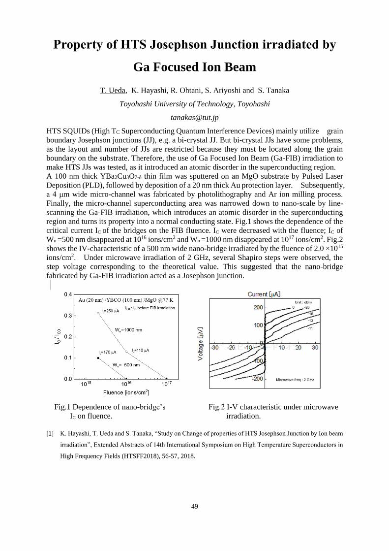
49
Property of HTS Josephson Junction irradiated by
Ga Focused Ion Beam
T. Ueda, K. Hayashi, R. Ohtani, S. Ariyoshi and S. Tanaka
Toyohashi University of Technology, Toyohashi
HTS SQUIDs (High TC Superconducting Quantum Interference Devices) mainly utilize grain
boundary Josephson junctions (JJ), e.g. a bi-crystal JJ. But bi-crystal JJs have some problems,
as the layout and number of JJs are restricted because they must be located along the grain
boundary on the substrate. Therefore, the use of Ga Focused Ion Beam (Ga-FIB) irradiation to
make HTS JJs was tested, as it introduced an atomic disorder in the superconducting region. A 100 nm thick YBa2Cu3O7-δ thin film was sputtered on an MgO substrate by Pulsed Laser
Deposition (PLD), followed by deposition of a 20 nm thick Au protection layer. Subsequently,
a 4 μm wide micro-channel was fabricated by photolithography and Ar ion milling process.
Finally, the micro-channel superconducting area was narrowed down to nano-scale by line-
scanning the Ga-FIB irradiation, which introduces an atomic disorder in the superconducting
region and turns its property into a normal conducting state. Fig.1 shows the dependence of the
critical current IC of the bridges on the FIB fluence. IC were decreased with the fluence; IC of
Wn =500 nm disappeared at 1016 ions/cm2 and Wn =1000 nm disappeared at 1017 ions/cm2. Fig.2
shows the IV-characteristic of a 500 nm wide nano-bridge irradiated by the fluence of 2.0 ×10¹⁵
ions/cm2. Under microwave irradiation of 2 GHz, several Shapiro steps were observed, the
step voltage corresponding to the theoretical value. This suggested that the nano-bridge
fabricated by Ga-FIB irradiation acted as a Josephson junction.
Fig.1 Dependence of nano-bridge’s Fig.2 I-V characteristic under microwave
IC on fluence. irradiation.
[1] K. Hayashi, T. Ueda and S. Tanaka, “Study on Change of properties of HTS Josephson Junction by Ion beam
irradiation”, Extended Abstracts of 14th International Symposium on High Temperature Superconductors in
High Frequency Fields (HTSFF2018), 56-57, 2018.

50
LTS SQUID magnetometers and gradiometers
G. Zhang1,2, Y. Wang1,2, S. Zhang1,2, X. Zhang1,2, L. Rong1,2, H. Dong1,2, L. Qiu1,2, J. Wu1,2,
Y. Pei1,2, Q. Tao1,2, L. You1,2 and X. Xie1,2
1State Key Laboratory of Functional Materials for Informatics, Shanghai Institute of
Microsystem and Information Technology (SIMIT), Chinese Academy of Sciences (CAS),
Shanghai
2Chinese Academy of Science, Center for Excellence in Superconducting Electronics,
Shanghai
In this work, we report the progress of LTS SQUID at SIMIT in China. As an ultra-
sensitive magnetic flux sensor, SQUIDs are widely used in many applications such as
biomagnetism, low-field magnetic resonance imaging, geophysics and so on. State-of-the-art
SQUIDs are mostly fabricated in Nb/Al-AlOx/Nb or NbN/AlN/NbN technology [1]. At SIMIT,
superconducting electronics facilities (SELF) have been built for superconducting integrated
circuits (SIC). SQUID fabrication benefits from the advance of superconducting process
technology. We present the fabrication of SQUID magnetometers and gradiometers designed
for some practical applications.
SQUID magnetometer consists of a washer-type SQUID and a flux transformer which
includes a pickup coil and an input coil to form a superconducting loop. The input coil is usually
integrated on the SQUID washer and thus inductively coupled to the SQUID by a mutual
inductance Min. In addition, some extra coils are integrated on chip to realize SQUID bootstrap
circuit [2]. To avoid the parasitic capacitance between SQUID and input coil, multi-loop
SQUID magnetometer is also presented. The noise performance of the SQUID magnetometer
is measured by using homemade readout electronics inside magnetically shielded room (MSR).
The magnetic field noise of <3fT/√Hz in white noise region has been obtained.
A gradient pickup coil is adopted in SQUID gradiometer. We present a planar first-order
gradiometer which is fabricated on 4-inch silicon wafer. Therefore, the baseline of the
gradiometer is limited to 3.5cm considering the integrated chip numbers. In MSR, the white
gradient field noise is measured to be better than 1fT/(cm*√Hz) [3].
Both magnetometer and gradiometer have been used in our practical systems, e.g.,
biomagnetism, transient electromagnetic detection and aeromagnetic survey. [1] Q. Liu, H. Wang, Q. Zhang, H. Wang, W. Peng and Z. Wang, Temperature-dependent performance of all-
NbN DC-SQUID magnetometers. (2016). Appl. Phys. Lett., 110 222604.
[2] X. Xie, Y. Zhang, H. Wang, Y. Wang, M. Mueck, H. Dong, H.-J. Krause, A. I. Braginski, A. Offenhaesser
and M. Jiang, A voltage biased superconducting quantum interference device bootstrap circuit. (2010).
Supercond. Sci. Technol. 23 065016. [3] X. Zhang, G. Zhang, Y. Wang, L. Rong, S. Zhang, J. Wu, L. Qiu, X. Xie and Z. Wang, A High-Balance
Planar SQUID Gradiometer. (2019). IEEE Transactions on Applied Superconductivity, 29 1600503.

51
LTS SQUID Based Transient Electromagnetic
System for Geophysical Prospecting
Y. Pei1,2, L. Rong1,2 , H. Dong1,2,Q. Tao1,2, J. Wu1,2, S. Zhang1,2, G. Zhang1,2, Y. Wang1,2, L.
Qiu1,2, L. You1,2 and X. Xie1,2
1State Key Laboratory of Functional Materials for Informatics, Shanghai Institute of
Microsystem and Information Technology (SIMIT), Chinese Academy of Sciences (CAS),
Shanghai
2Chinese Academy of Science, Center for Excellence in Superconducting Electronics,
Shanghai
Transient ElectroMagnetic (TEM) prospecting is widely used in mineral, groundwater, and
geothermal exploration. Compared with commonly used induction coils, Low-temperature
Superconducting Quantum Interference Devices (LTS SQUIDs) can act as a magnetic field
receiver with better performance, e.g. wider bandwidth, lower noise level(7 fT/Hz) and less
distortion, thus leading to higher shallow ground surveying accuracy and deeper exploration
depth.
In this work, we will first introduce the development of the LTS SQUID based TEM system
developed at SIMIT in China. The system bandwidth is greater than 500 kHz and its slow rate
achieves approximately 28mT/s(Dual-Channel Squid-Based TEM System). A home-made
TEM transmitter can generate strong current pulses with different pulse widths according to
different ground resistivity. With this TEM system, we successfully observed the sign-reversal
signals, which implies the induced-polarization effect. However the negative amplitude is
always bigger than modeling, we revealed the reason for the sign-reversal signals is the primary
field switch-off procedure .
We then carried out field tests in different provinces in China, such as Shanghai, Jilin,
Inner Mongolia, Henan, Yunnan, as well as in Tajikistan. Some latest results of TEM survey
in these area will be presented.
[1] Shangyu Du, Yi Zhang, Yifeng Pei, Kun Jiang, Liangliang Rong, Changchun Yin, Yanju, Ji, and Xiaoming
Xie. Study of transient electromagnetic method measurements using a superconducting quantum interference
device as B sensor receiver in polarizable survey area, Geophysics, 83(2), E111-116. 2018,
doi.org/10.1190/geo2017-0197.1
[2] Liangliang Rong, Suxin Bao, Jun Wu, Guofeng Zhang, Longqing Qiu, Shunlin Zhang, Yongliang Wang,
Hui Dong, Yifeng Pei, and Xiaoming Xie. High-Performance Dual-Channel Squid-Based TEM System
and Its Application. IEEE Transactions on Applied Superconductivity VOL. 29, NO. 8, DECEMBER 2019

52
Control of roughness and stress of Nb films for
Nb/Al‐AlOx/Nb Josephson junctions
Yu Wu1,3,4, Liliang Ying1,4, Jie Ren1,2,4, Wanning Xu1,2,4, Yingyi Shao1,2,4, Liyun Chen1,2,4,
Xue Zhang1,2,4, Xiaoping Gao1,4, Wei Peng1,2,4, Masaaki Maezawa1,4, Zhen Wang1,2,3,4
1Key laboratory of functional materials for informatics, Shanghai Institute of Microsystem
and Information Technology (SIMIT), Chinese Academy of Science (CAS), Shanghai.
2Univerisity of Chinese Academy of Science, Beijing.
3ShanghaiTech University, Shanghai.
4CAS Center for Excellence in Superconducting Electronics (CENSE), Shanghai.
Abstract—Nb/Al-AlOx/Nb Josephson junctions are the most fundamental components in
Rapid Single Flux Quantum (RSFQ) circuits. Very large-scale RSFQ integration often has a
strict requirement on wafer-scale junction qualities. In particular, Nb film stress and roughness
in Nb/Al-AlOx/Nb trilayer-based Josephson junctions are two important factors affecting their
qualities. In our previous work, a two-step sputtering technique was developed to prepare Nb
films with different combinations of stress and roughness conditions to study the influence of
stress and roughness on junction qualities separately, in which the film consisting of two
sublayers deposited in-situ at different sputtering Ar pressures. In this paper, we found that a
cooling procedure between the sublayer depositions improves the reproducibility of the total
stress and roughness. Besides, changing the sputtering rate and thickness of the two sublayers
has been studied to investigate the impact of the different total stress and surface roughness
conditions.
53
Tunable Josephson junction based on black
phosphorus
Zuyu Xu, Wei Chen, Wanghao Tian, Yangyang Lv, Shixian Chen, Xianjing Zhou,
Sining Dong, Jun Li, Yonglei Wang, Huabing Wang*, and Peiheng Wu
Research Institute of Superconductor Electronics (RISE), Nanjing University, Nanjing.
In Josephson junctions, the physical properties of barrier layers play a key role in the tunneling
behavior of the junctions [1, 2]. Black phosphorus (BP), a two-dimensional layered material
with semiconductor properties, has been expected to be used for tuning the characteristics of
Josephson junctions as a barrier layer. Here, we applied an in-situ technique to fabricate a
Josephson junction with few-layer BP sandwiched by two niobium electrodes. It is shown that
the oxidization and interfacial degradation of BP can be well reduced, and the sputtered Nb
films can make ohmic contacts to the BP thin flakes. According to strong anisotropy of BP, we
show that the nonuniform tunneling current distribution in the junctions where supercurrent
density distribution peaked at the edges of the junctions since these are reflected in unique
features of the dependence of critical current on applied magnetic fields. Our results
demonstrate that the nonuniform supercurrent distribution dominates the Josephson tunneling
owing to the superior in-plane transport properties of BP, and the supercurrent can be well
modified by applying the ionic gel electrolyte gate. These observations could open a new
pathway for the applications of superconductor quantum circuits.
We gratefully acknowledge financial support by the National Natural Foundation of China
(Grants No.61727805, 11234006).
[1] Heersche, H.B., Jarillo-Herrero, P., Oostinga, J.B., Vandersypen, L.M. & Morpurgo, A.F. (2007). Bipolar
supercurrent in graphene. Nature 446, 56-59.
[2] Lee, G.H., Kim, S., Jhi, S.H. & Lee, H.J. (2015). Ultimately short ballistic vertical graphene Josephson
junctions. Nat Commun 6, 6181.
[3] Zhu, Y.Y. at el. (2019). Isotropic Josephson tunneling in c-axis twist bicrystals of Br2Sr2CaCu2O8+ᵹ.
Preprint at https://arxiv.org/abs/1903.07965

54
Novel Nb-based Josephson junctions using
Bi2Sr2CaCu2O8+δ as barriers
Shixian Chen, Wanghao Tian, Zuyu Xu, Tong Qing, Wenchen Yue,Sining Dong, Yonglei
Wang, Huabing Wang*, and Peiheng Wu
Research Institute of Superconductor Electronics, Nanjing University, Nanjing.
High quality Nb-based Josephson junctions with various types of barriers have been employed
in voltage standards, terahertz receivers, SQUIDs, and many other applications. Tunable
junction parameters are required for novel applications, e.g. in superconducting quantum
circuits. On the other hand, Bi2Sr2CaCu2O8+δ (B2212) single crystals, typically used as
superconducting material, may have more applications due to their atomically smooth surface,
phase transition, etc [1, 2, 3]. In our experiment, B2212 flakes with large area can be obtained
by a new nano-fabrication technique. A novel Josephson junction device with a non-
superconducting B2212 flake as its barrier was fabricated by an in-situ transferring technique.
Observed have been typical current-voltage characteristics satisfying the resistively-shunted-
junction model, and clear Shapiro steps under 10-40 GHz microwave irradiation. The vertical
structure of Nb-B2212-Nb was inspected by SEM and Raman spectrum. A tunable Josephson
junction device is expected by controlling the phase transition of the B2212 barrier in the near
future.
We gratefully acknowledge financial support by the National Natural Science Foundation of
China (No. 61727805), the National Key R&D Program of China (2018YFA0209002).
[1] Y. Koval, X. Jin, C. Bergmann, Y. Simsek, L. Özyüzer, P. Müller, H. B. Wang, G. Behr, and B. Büchner.
(2010). Tuning superconductivity by carrier injection. Appl. Phys. Lett., 96, 082507.
[2] M. H. Liao, Y. Y. Zhu, J. Zhang, R. Zhong, J. Schneeloch, G. Gu, K. Jiang, D. Zhang, X. C. Ma, and Q. K.
Xue. (2018). Superconductor-Insulator Transitions in Exfoliated Bi2Sr2CaCu2O8+δ Flakes. Nano Lett., 18,
5660-5665.
[3] Zhu, Y. Y. at el. (2019). Isotropic Josephson tunneling in c-axis twist bicrystals of Br2Sr2CaCu2O8+ᵹ.
Preprint at https://arxiv.org/abs/1903.07965.

55
Proximity Effects on Mo/Cu Bilayers
F.J. Li, W. Cui, J. Ding, R. Huang, X.Y. Hua, H. Jin, Y.J. Liang, G.L. Wang, S.F. Wang, Y.R.
Wang, Y. Zhou and Y.N. Zhang
Department of Astronomy and Tsinghua Center for Astrophysics, Tsinghua University,
Beijing.
Hot Universe Baryon Surveyor (HUBS) space project has been proposed in China to implement
the science theme “the missing baryons”. One of the core parts of HUBS is the X-ray
spectrometer with a designed energy resolution of 2 eV@ 0.6. keV, as a high resolution
microcalorimeter made of a large array of Transition Edge Sensors. Superconducting transition-
edge sensors (TESs) as highly sensitive thermometer and/or photodetectors, have been widely
developed for potential applications of measurement across the electromagnetic spectrum from
millimeter through gamma rays as well as with weakly interacting particles in variety of
astronomical instruments. Due to their capabilities of achieving high energy resolution, tunable
transition temperature, and excellent noise limitation, proximity bilayers superconductors are
attractive for use in TES detectors. Particularly for cryogenic microcalorimeters in detecting x-
rays and gamma-rays, Molybdenum/copper (Mo/Cu) bilayers are among the most suitable
materials, which exhibit good environmental stability and provide low resistivity films to attain
adequate thermal conductivity. Here, we report a number of Mo/Cu bilayers fabricated on
silicon nitride-on-silicon (Si3N4-on-Si) by using sputtering with ultra-high vacuum, and the
low-temperature electrical characterization of these bilayers. Experimental data are analyzed
on the base of Usadel equations, in which the proximity effect in the bilayer is mainly governed
by the interface transparency between the superconductor and the normal metal, and the
superconducting critical temperature (Tc) of the superconductor. Figure 1(b) indicates that the
proximity effect model with well described behavior of Tc shows much less Tc with increased
the thickness of the normal metal. And figure 1(a) shows very narrow superconducting
transitions in R(T) curves, which could evidence the high quality of the interface. We also found
that the fabricated bare rectangle Mo/Cu bilayers have achieved Tc<100 mK, with typical Mo
single film Tc around 1.05 K. It should be noted that the variation of Tc with similar Cu thickness
of samples is mainly due to the pre-grown condition being different.
0.1 0.2 0.3 0.4
0.0
0.2
0.4
0.6
0.8
1.0
R/R
n
T (K)
75 nm
100 nm
150 nm
(a)
50 100 150 200 250
0.0
0.1
0.2
0.3
0.4
Measured
Fit
Tc
(K)
Thickness of Cu film (nm)
(b)
Fig. 1 (a) Normalized R(T) curve of Mo/Cu bilayers; (b) Tc as a function of Cu thickness for Mo/Cu bilayers
(Line is fit to proximity effect based on Usadel equations).

56
Development of Mo/Cu TES Devices
S.F. Wang, W. Cui, J. Ding, R. Huang, X.Y. Hua, H. Jin, F.J. Li, Y.J. Liang, G.L. Wang, Y.R.
Wang, Y.N. Zhang and Y. Zhou
Department of Astrophysics and Tsinghua Center for Astrophysics, Tsinghua University,
Beijing.
The Hot Universe Baryon Surveyor (HUBS) mission, aiming at addressing the issue of
“missing baryons” in the local universe, requires a superconducting transition-edge sensor (TES)
array with high energy resolution. Here we report the recent progress on developing the Mo/Cu
TES for HUBS.

57
Characterization of Sputtered Molybdenum Thin
Films
Y.R. Wang, W. Cui, J. Ding, R. Huang, X.Y. Hua, H. Jin, F.J. Li, Y.J. Liang, G.L. Wang, S.F.
Wang, Y.N. Zhang and Y. Zhou
Department of Astronomy and Tsinghua Center for Astrophysics, Tsinghua University,
Beijing
Molybdenum thin films have shown great potential in the development of high-performance
superconducting transition-edge sensors (TESs). Used in combination with a normal metal (e.g.,
copper or gold) in a bilayer film, the stress and crystalline structure of the Mo layer can affect
the residual resistivity ratio (RRR) of the bilayer, as well as the interface between the
superconducting and normal layers, and thus also the superconducting transition temperature
(Tc) of the bilayer. In this work, molybdenum is deposited on a Si3N4 film over a silicon
substrate with radiofrequency magnetron sputtering. A set of Mo films are produced with
different sputtering power and argon pressure; growth time is adjusted to keep all of the films
a roughly the same thickness. Stress is measured by calculating the curvature variation before
and after the deposition of a Mo film. The morphology and crystalline structure of the films are
characterized with a variety of techniques, including atomic force microscopy, scanning
electron microscopy, and transmission electron microscopy. It is found that the film crystalline
structure and surface roughness are strongly dependent on the sputtering power and deposition
pressure. X-ray reflectivity and X-ray diffraction measurements are also performed to measure
the density, thickness, surface roughness, grain size and residual stress of the films; the results
exhibit good consistency with those obtained with other methods. The resistivity, RRR and Tc
of the films are also measured. We present correlations (or lack thereof) between the Tc of the
Mo films and their measured morphological, mechanical, or electrical properties.
This research is conducted as a part of the development of Mo-Cu TES devices for a proposed
X-ray astronomical mission, HUBS.

58
Bi-2212 mesas made of Bi-2212 thin film for THz
emission with superior heat dissipation.
Takahiro Murakami and Kensuke Nakajima
Graduate School of Science and Engineering, Yamagata University, Yonezawa.
SIS layered structure included in the crystal structure of the high temperature superconductor
Bi2Sr2CaCu2O8 (Bi-2212) functions as an intrinsic Josephson junction (IJJ). Since the
superconducting energy gap frequency is high enough for terahertz regime, Bi-2212 crystals
faceted to be a THz cavity shape, that is IJJ as well, emits THz wave when the ac Josephson
frequency proportional to junction voltage across the interior SIS junctions matches the cavity
resonance frequencies. The first strongly monochromatic terahertz wave emission from Bi-
2212 IJJ was reported from mesa IJJ formed on ab-plane of bulk single crystal[1]. The organic
adhesive layer between the thick basal crystal of the mesa and the dielectric substrate prevents
heat dissipation from the voltage biased IJJ. In order to improve heat dissipation, a structure
called a stand-alone mesa which removed the basal crystal of mesa IJJ have been proposed.
However, either mesa or stand-alone mesa, these devices produced from fine bulk crystals are
artisanal product and are not suitable for industrial production. We have been developing of IJJ
made of Bi-2212 thin films grown on MgO substrates suitable for industrial production, and
succeeded in emitting terahertz wave of about 6 μW at frequency of 0.6 THz in a wide
temperature range from 60 K to 75 K, so far. This result suggested high heat dissipation of the
thin film type Bi-2212 IJJ without organic adhesive layer. On the other hand, the strongest
terahertz wave emission (30 µW, 0.438 THz, 55 K) from Bi-2212 IJJ has been reported from
the mesa IJJ with a thin basal crystal and a junction height of 2.8 µm[2]. This result indicates
the high performance of the mesa junction which overcomes the heat dissipation. Theoretically,
considering that the THz radiation intensity is proportional to the square of the number of
coherently oscillating junctions. It is considered that the key issue of strong terahertz wave
radiation is how many junctions can be kept at the optimum operating temperature to be
synchronized.
In this study, we fabricated Bi-2212 thin film mesa-type IJJ junctions using Bi-2212 thin film
to clarify its heat dissipation and terahertz wave radiation performance. We propose a metal
mask process to form a mesa IJJ as high as possible on Au/Bi-2212 thin films. A rectangular
shape 500 nm thick Nb thin film as shown in figure 1
formed on Au/Bi2212 film by reactive ion etching to be a
junction defining metal mask to withstand long time Ar ion
milling. We have fabricated IJJ with sufficient junction
height and thin basal crystal on Bi-2212 thin film by the Nb
metal mask process. We will report the voltage-current
characteristics and THz radiation characteristics of
junctions with excellent heat dissipation. [1] L. Ozyuzer et al., Science, 318 1291 (2007).
[2] S. Sekimoto et al., APPLIED PHYSICS LETTERS 103, 182601
(2013).
Fig 1. Photomicrograph of the Nb
mask formed on Au/Bi-2212 film.

59
High-power terahertz emission from Bi2Sr2CaCu2O8
intrinsic Josephson junction stacks
Z. D. Qi, H. C. Sun, H. L. Zhang, T. Qing, J. Shi, X. J. Zhou,H. B. Wang*, and P. H. Wu
Research Institute of Superconductor Electronics (RISE), Nanjing University, Nanjing.
The terahertz (THz) wave is at a special position in the electromagnetic spectrum, which has
attracted much attention owing to its extensive potential applications, such as imaging, medical
diagnostics, public security, macromolecule detection, and environmental monitoring. These
practical applications need the developing of powerful continuous-wave emitters. The terahertz
generators made with stacks of intrinsic Josephson junctions (IJJs) in high critical temperature
(high-Tc) superconductor Bi2Sr2CaCu2O8 (BSCCO) are promising candidates [1, 2].
BSCCO can be regarded as a lot of Josephson junctions in series, and a 1μm thick BSCCO
stack contains about 667 junctions. Known by the ac Josephson effects, when the current
flowing through Josephson junctions is larger than the critical current (Ic), the junctions oscillate
at a frequency f = V/NΦ0, where V, N, and Φ0 are the voltage across the stack, the number of
Josephson junctions, and the flux quantum respectively. However, the relatively low output
power has always been an important factor limiting the practical applications.
In order to get higher emission power, a new “in-line” fabrication method is used to make the
sample containing more than 1000 Josephson junctions easily, and diamond substrates are used
for higher thermal conductivity. Thanks to the above-mentioned efforts, a round shape BSCCO
stack with a diameter of 200 μm, thickness of 1.65 μm is fabricated, with a record high emission
power of 258 μW at 54 K by direct detection, a frequency range of 200 to 950 GHz, and an
operating temperature up to 83 K.
Taking into account the optical path of the terahertz interferometer, we think that most of the
electromagnetic waves released by Josephson oscillation dissipate in the optical path. Inferring
from previous experimental results [3], the actual output power of this sample is about 846 μW.
Considering the radiation directionality, the output power may exceed 1 mW. This work greatly
increases the power of a single BSCCO terahertz source and improves its potential practice
value.
We gratefully acknowledge financial support by the National Natural Foundation of China
(Grants No.61727805, 11234006).
[1] L. Ozyuzer and et al, Emission of coherent THz radiation from superconductors, Science 318, 1291 (2007).
[2] H. B. Wang and et al, Coherent THz emission of intrinsic Josephson junction stacks in the hot spot regime,
Phys. Rev. Lett. 105, 057002 (2010).
[3] D. Y. An and et al, Terahertz emission and detection both based on high-Tc superconductors: Towards an
integrated receiver, Appl. Phys. Lett. 102, 092601 (2013).

60
Characterization of superconducting NbN hot-
electron bolometers as THz direct detectors
R. F. Su, X. C. Tu, J. B. Wu, X. Q. Jia, C. H. Zhang, L. Kang, B. B. Jin, W. W. Xu, H. B. Wang,
J. Chen and P. H. Wu
Research Institute of Superconductor Electronics (RISE), School of Electronic Science and
Engineering, Nanjing University, Nanjing.
During the past decades, superconducting hot electron bolometers (HEBs) based on the niobium
nitride (NbN) films have been widely used as heterodyne detectors (mixers) near liquid-helium
temperatures at frequencies above 1.2 THz in astronomy [1]. Due to their short response time
and high sensitivity, superconducting HEBs are also been used as THz direct detectors for the
applications in biology, medicine and security systems recently [2].
We compared the performance of an HEB direct detector at 0.65 THz with thermal, microwave
(MW) and THz biasing methods based on DC readout scheme. The current responsivity of the
NbN HEB detector with appropriate MW and THz biasing is significantly higher (about one
order) than that with thermal biasing. An optical NEP at the order of pW/√Hz is obtained by
choosing the MW frequency and power appropriately. The MW frequencies are usually around
1 GHz within the IF bandwidth of the mixer. With appropriate MW biasing, the NEP shows no
deterioration and achieves a slight improvement compared with thermal biasing. It is feasible
to replace the method of thermal biasing with MW biasing especially for a multi-pixel HEB
detector array. Furthermore, relaxation oscillations in the bi-stable region of the HEB detectors
have been studied using a microwave probe as a tool. The frequency of relaxation oscillations
switching between the superconducting and resistive states increases linearly with incident THz
power but nonlinearly with bias voltage or bath temperature. The strong periodic pulse trains
of relaxation oscillations have a maximum duty cycle of ~50%. In addition to relaxation
oscillations, we also see weaker oscillations when the HEB is in the resistive state, which we
call intrinsic oscillations. These have a constant frequency at the order of 10 kHz. Based on the
linear dependence of the relaxation oscillation frequency on the incident THz power, one can
make a digital THz power measurement from a few nW to about 1 μW. [1] J. Chen, Y. Jiang, M. Liang, L. Kang, B. B. Jin, W. W. Xu and P. H. Wu, (2011). Stability of superconducting
hot electron bolometer receivers. IEEE Trans. Appl. Supercond., 21(3), 667-670.
[2] R. F. Su, Y. D. Zhang, X. C. Tu X C, X. Q. Jia, L. Kang, B. B. Jin, W. W. Xu, J. Chen and P. H. Wu, (2019).
Terahertz direct detectors based on superconducting hot electron bolometers with different biasing methods.
IEEE Trans. Appl. Supercond, 29(5), 2300104.
[3] R. F. Su, Y. D. Zhang, X. C. Tu, X. Q. Jia, C. H. Zhang, L. Kang, B. B. Jin, W. W. Xu, H. B. Wang, J. Chen,
and P. H. Wu, (2019). Microwave probing of relaxation oscillations related to terahertz power detection in
superconducting hot electron bolometers. Supercond. Sci. Technol., 32, 105002.

61
The application of high-Tc SQUID-based low-field
NMR in human liver tumor discrimination
Shu-Hsien Liao1, Hao-Wei Huang1, Yu-Ting Liao1, Jhih-Hao Chen1, Kai-Wen Huang2,
Herng-Er Horng1
1Institute of Electro-Optical Engineering, National Taiwan Normal University, Taipei
116, Taiwan
2Department of Surgery and Hepatitis Research Center, National Taiwan University
Hospital, Taipei 100, Taiwan
Superconducting quantum interference device is the most sensitive sensor for magnetic field
detection. Therefore SQUID-based nuclear magnetic resonance spectrometer promises the
advantages of low cost and high sensitivity. In this study, a home-made high-Tc SQUID NMR
spectrometer was set up for tumor tissue discrimination. The T1 relaxation time of normal liver
tissues and cancerous tissues in Low Field nuclear magnetic resonance were obtained. After
detecting 30 pairs of human liver specimens, the significant difference of T1 relaxation times
was found to reveals the feasibility for liver cancer tissue discrimination by using low-field
NMR.