Embed Size (px)
Citation preview
10.2417/spepro.005250
To optimize nanofabrication,consider unique traitsZhifu Yin, E Cheng, and Helin Zou
With optimized parameters, nano hot embossing can create high-
quality patterns again and again.
In recent years, the study of nanofluidic systems has been reported in a
wide spectrum of fields, including chemistry, biology, and medicine.1–3
Researchers use nanofluidic systems to study the behavior, manipula-
tion, and control of fluids confined to nanosized structures. Recent pub-
lications have highlighted applications such as protein analysis,1, 2, 4
DNA extension,5–7 and ion separation8, 9 based on nanofluidic devices.
One fabrication technique for nanofluidic devices, called hot emboss-
ing, entails squishing together a polymer material and a mold at
elevated temperature. This technique enables the creation of 2D or
3D structures by applying appropriate temperature, pressure, and time.
In contrast to conventional nanofabrication methods such as litho-
graphy and etching on semiconductor substrates, the hot embossing
method has demonstrated considerably better results in terms of cost,
resolution, productivity, and ease of operation. However, during hot
embossing the processing parameters must be optimized to fabricate
nanostructures with high replication accuracy.
We developed numerical simulations for the hot embossing process
using 2D polyethylene terephthalate (PET) nanochannel fabrication as
a model system. We used the generalized Maxwell model to optimize
the processing parameters, but calculated the constants with a newly
established fitting formula rather than by the conventional method.
Traditionally, the constants of the generalized Maxwell model are
based on the tensile stress relaxation test.10–12 However, hot emboss-
ing is a compressive process. In most cases the compressive behavior
of a given viscoelastic polymer and its tensile behavior follow very
different curves.13, 14 In addition, the cross-sectional area of the poly-
mer substrate is usually assumed to be constant during stress relaxation
tests. During a hot embossing process, however, the cross-sectional
area varies with time. Therefore, the material parameters calculated by
tensile tests may not be applicable to hot embossing.
Here, the constants of the generalized Maxwell model were calcu-
lated with a newly established fitting formula based on experimen-
tal compressive creep tests, and consider the change in the polymer’s
cross-sectional area during the embossing process.
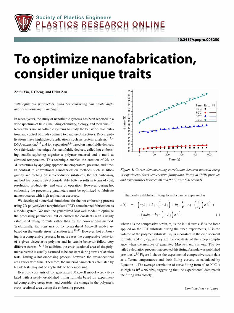
Figure 1. Curves demonstrating correlations between material creep
in experiment (dots) versus curve-fitting data (lines), at 3MPa pressure
and temperatures between 60 and 90◦C, over 500 seconds.
The newly established fitting formula can be expressed as
" .t/ D
��0b1 C b1 �
F
V� A1
�C b2 �
F
V� A1 �
�1
�J
�e
�t�J � t
C
��0b2 � b1 �
F
V� A1
�e
�t�J ; (1)
where " is the compressive strain, �0 is the initial stress, F is the force
applied on the PET substrate during the creep experiments, V is the
volume of the polymer substrate, A1 is a constant in the displacement
formula, and b1, b2, and �J are the constants of the creep compli-
ance when the number of generated Maxwell units is one. The de-
tailed calculation process that created this fitting formula was published
previously.15 Figure 1 shows the experimental compressive strain data
at different temperatures and their fitting curves, as calculated by
Equation 1. The average correlation of curve fitting from 60 to 90◦C is
as high as R2 D 96.66%, suggesting that the experimental data match
the fitting data closely.
Continued on next page
10.2417/spepro.005250 Page 2/4
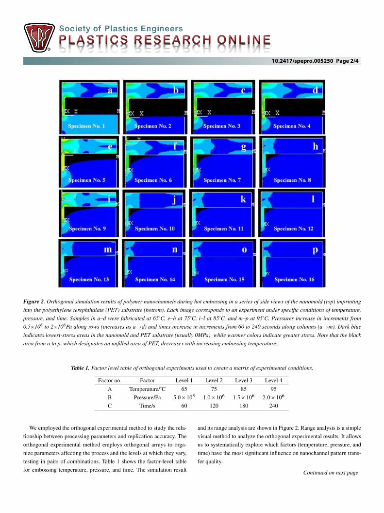
Figure 2. Orthogonal simulation results of polymer nanochannels during hot embossing in a series of side views of the nanomold (top) imprinting
into the polyethylene terephthalate (PET) substrate (bottom). Each image corresponds to an experiment under specific conditions of temperature,
pressure, and time. Samples in a–d were fabricated at 65◦C, e–h at 75◦C, i–l at 85◦C, and m–p at 95◦C. Pressures increase in increments from
0.5�106 to 2�106Pa along rows (increases as a!d) and times increase in increments from 60 to 240 seconds along columns (a!m). Dark blue
indicates lowest-stress areas in the nanomold and PET substrate (usually 0MPa), while warmer colors indicate greater stress. Note that the black
area from a to p, which designates an unfilled area of PET, decreases with increasing embossing temperature.
Table 1. Factor level table of orthogonal experiments used to create a matrix of experimental conditions.
Factor no. Factor Level 1 Level 2 Level 3 Level 4
A Temperature/◦C 65 75 85 95
B Pressure/Pa 5:0 � 105 1:0 � 106 1:5 � 106 2:0 � 106
C Time/s 60 120 180 240
We employed the orthogonal experimental method to study the rela-
tionship between processing parameters and replication accuracy. The
orthogonal experimental method employs orthogonal arrays to orga-
nize parameters affecting the process and the levels at which they vary,
testing in pairs of combinations. Table 1 shows the factor-level table
for embossing temperature, pressure, and time. The simulation result
and its range analysis are shown in Figure 2. Range analysis is a simple
visual method to analyze the orthogonal experimental results. It allows
us to systematically explore which factors (temperature, pressure, and
time) have the most significant influence on nanochannel pattern trans-
fer quality.
Continued on next page
10.2417/spepro.005250 Page 3/4
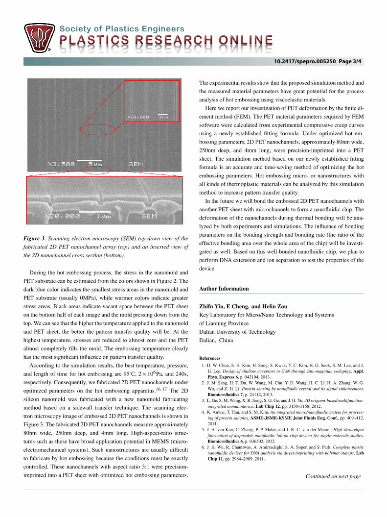
Figure 3. Scanning electron microscopy (SEM) top-down view of the
fabricated 2D PET nanochannel array (top) and an inserted view of
the 2D nanochannel cross section (bottom).
During the hot embossing process, the stress in the nanomold and
PET substrate can be estimated from the colors shown in Figure 2. The
dark blue color indicates the smallest stress areas in the nanomold and
PET substrate (usually 0MPa), while warmer colors indicate greater
stress areas. Black areas indicate vacant space between the PET sheet
on the bottom half of each image and the mold pressing down from the
top. We can see that the higher the temperature applied to the nanomold
and PET sheet, the better the pattern transfer quality will be. At the
highest temperature, stresses are reduced to almost zero and the PET
almost completely fills the mold. The embossing temperature clearly
has the most significant influence on pattern transfer quality.
According to the simulation results, the best temperature, pressure,
and length of time for hot embossing are 95◦C, 2 � 106Pa, and 240s,
respectively. Consequently, we fabricated 2D PET nanochannels under
optimized parameters on the hot embossing apparatus.16, 17 The 2D
silicon nanomold was fabricated with a new nanomold fabricating
method based on a sidewall transfer technique. The scanning elec-
tron microscopy image of embossed 2D PET nanochannels is shown in
Figure 3. The fabricated 2D PET nanochannels measure approximately
80nm wide, 250nm deep, and 4mm long. High-aspect-ratio struc-
tures such as these have broad application potential in MEMS (micro-
electromechanical systems). Such nanostructures are usually difficult
to fabricate by hot embossing because the conditions must be exactly
controlled. These nanochannels with aspect ratio 3:1 were precision-
imprinted into a PET sheet with optimized hot embossing parameters.
The experimental results show that the proposed simulation method and
the measured material parameters have great potential for the process
analysis of hot embossing using viscoelastic materials.
Here we report our investigation of PET deformation by the finite el-
ement method (FEM). The PET material parameters required by FEM
software were calculated from experimental compressive creep curves
using a newly established fitting formula. Under optimized hot em-
bossing parameters, 2D PET nanochannels, approximately 80nm wide,
250nm deep, and 4mm long, were precision-imprinted into a PET
sheet. The simulation method based on our newly established fitting
formula is an accurate and time-saving method of optimizing the hot
embossing parameters. Hot embossing micro- or nanostructures with
all kinds of thermoplastic materials can be analyzed by this simulation
method to increase pattern transfer quality.
In the future we will bond the embossed 2D PET nanochannels with
another PET sheet with microchannels to form a nanofluidic chip. The
deformation of the nanochannels during thermal bonding will be ana-
lyzed by both experiments and simulations. The influence of bonding
parameters on the bonding strength and bonding rate (the ratio of the
effective bonding area over the whole area of the chip) will be investi-
gated as well. Based on this well-bonded nanofluidic chip, we plan to
perform DNA extension and ion separation to test the properties of the
device.
Author Information
Zhifu Yin, E Cheng, and Helin Zou
Key Laboratory for Micro/Nano Technology and Systems
of Liaoning Province
Dalian University of Technology
Dalian, China
References
1. D. W. Chun, S. H. Kim, H. Song, S. Kwak, Y. C. Kim, H. G. Seok, S. M. Lee, and J.H. Lee, Design of shallow acceptors in GaN through zinc-magnium codoping, Appl.Phys. Express 6, p. 042104, 2013.
2. J. M. Sang, H. T. Du, W. Wang, M. Chu, Y. D. Wang, H. C. Li, H. A. Zhang, W. G.Wu, and Z. H. Li, Protein sensing by nanofluidic crystal and its signal enhancement,Biomicrofluidics 7, p. 24112, 2013.
3. L. Ge, S. M. Wang, X. R. Song, S. G. Ge, and J. H. Yu, 3D origami-based multifunction-integrated immunodevice, Lab Chip 12, pp. 3150–3158, 2012.
4. K. Anwar, T. Han, and S. M. Kim, An integrated micro/nanofluidic system for process-ing of protein samples, ASME-JSME-KSME Joint Fluids Eng. Conf., pp. 409–412,2011.
5. J. A. van Kan, C. Zhang, P. P. Malar, and J. R. C. van der Maarel, High throughputfabrication of disposable nanofluidic lab-on-chip devices for single molecule studies,Biomicrofluidics 6, p. 036502, 2012.
6. J. H. Wu, R. Chantiwas, A. Amirsadeghi, S. A. Soper, and S. Park, Complete plasticnanofluidic devices for DNA analysis via direct imprinting with polymer stamps, LabChip 11, pp. 2984–2989, 2011.
Continued on next page
10.2417/spepro.005250 Page 4/4
7. J. N. Pedersen, R. Marie, D. L. V. Bauer, K. H. Rasmussen, M. Yusuf, E. V. Volpi,A. Kristensen, K. U. Mir, and H. Flyvbjerg, Fully stretched single DNA molecules ina nanofluidic chip show large-scale structural variation, Biophys. J. 104 (2), p. 175a,2013.
8. T. Tsukahara, Nanofluidic-based separation system of radionuclide ions by controllingelectrostatic forces, Bull. Res. Lab. Nuclear Reactors 34, p. 51, 2013.
9. D. Gillespie and S. Pennathur, Separation of ions in nanofluidic channels with com-bined pressure-driven and electro-osmotic flow, Anal. Chem. 85, pp. 2991–2998,2013.
10. N. W. Kim, K. W. Kim, and H. C. Sin, Finite element analysis of low temperaturethermal nanoimprint lithography using a viscoelastic model, Microelectron. Eng. 85,p. 1858, 2008.
11. S. H. Lan, H. J. Lee, S. H. Lee, J. Ni, X. M. Lai, H. W. Lee, J. H. Song, and M. G.Lee, Experimental and numerical study on the viscoelastic property of polycarbonatenear glass transition temperature for micro thermal imprint process, Mater. Des. 30,p. 3879, 2009.
12. Z. Z. Gao, W. Liu, Z. Q. Liu, and Z. F. Yue, Experiment and simulation study on thecreep behavior of PMMA at different temperatures, Polym.-Plast. Technol. Eng. 49,p. 1478, 2010.
13. R. N. Haward, B. M. Murphy, and E. F. T. White, Relationship between compressiveyield and tensile behavior in glassy thermoplastics, J. Polym. Sci. Pt. B-Polym. Phys.9, pp. 801–814, 1971.
14. R. Elleuch and W. Taktak, Viscoelastic behavior of HDPE polymer using tensile andcompressive loading, J. Mater. Eng. Perform. 15, p. 111, 2006.
15. Z. F. Yin, E. Cheng, H. L. Zou, and P. Jurcıcek, Analysis of polymer viscoelastic proper-ties based on compressive creep tests during hot embossing for two-dimensional poly-ethylene terephthalate nanochannels, Polym. Eng. Sci., 2013. First published online:29 October
16. E. Cheng, H. L. Zou., Z. F. Yin, P. Jurcıcek, and X. Zhang, Fabrication of 2D polymernanochannels by sidewall lithography and hot embossing, J. Micromech. Microeng.23, p. 075022, 2013.
17. J. Rao, H. L. Zou, R. R. A. Syms, and E Cheng, Fabrication of 2D silicon nano-moldbased on sidewall transfer, Micro Nano Lett. 6, p. 29, 2011.
c 2014 Society of Plastics Engineers (SPE)