Embed Size (px)
Citation preview

NJM2552
- 1 - Ver.2018-03-23
100MHz INPUT MIXER AND 450kHz FM/AM IF DEMODULATOR IC GENERAL DESCRIPTION PACKAGE OUTLINE
The NJM2552 is a FM IF demodulator IC with 450kHz (standard) IF input, which operates from 2.2V to 9.0V supply. It includes an oscillator, mixer, limiting amplifier, FM/AM detectors, and RSSI circuit. The NJM2552 is suitable for FM /AM receivers for data / voice radio systems. NJM2552V
FEATURES Wide Operating Voltage 2.2V to 9.0V Low Operating Current FM: 2.5mA at V+ =2.7V, AM SW =LOW
AM and FM: 5mA at V+ =2.7V, AM SW =HIGH Maximum Mixer Input Frequency 100MHz (reference value) IF Frequency 450kHz (standard) AM/FM detector circuits selectable
AM SW= HIGH Simultaneous operation of AM/FM sections AM SW= LOW FM section only
Built-in AGC circuit in AM section Wide Range RSSI (Received Signal Strength Indication) Bipolar Technology Package Outline SSOP20
BLOCK DIAGRAM
OSC(B)
AM IFIN
V+
AMDEC
FM IFOUT
AM AFOUT
AMPOUT
OSC(E)
MIXOUT
AMSW
RSSIOUT
RF AGCOUT
MIXIN
GND FM IF IN
FM AFOUT
QUADIN
AMPIN
AM AGCIN
FMDEC
16 15 14 13 12 11
101 2 43 5 6 7 8
FM AMP FMDET
AMP
OSCAMP
MIXER
9
17181920
RSSI
-A
AM AMP
AMDET
AGC+ - +
-

NJM2552
- 2 - Ver.2018-03-23
ABSOLUTE MAXIMUM RATINGS (Ta=25°C)
PARAMETER SYMBOL RATINGS UNIT
Supply Voltage V+ 12 V
Power Dissipation P d 300 mW
Operating Temperature T o p r -40 to +85 °C
Storage Temperature T s t g - 50 to +125 °C
RECOMMENDED OPERATING CONDITION (Ta=25°C)
PARAMETER SYMBOL CONDITIONS MIN. TYP. MAX. UNIT
Supply Voltage V+ 2.2 2.7 9.0 V
ELECTRICAL CHARACTERISTICS
Ta=25°C, V+=2.7V, fMIX=10.7MHz, fLO=10.25MHz, fIF=450kHz, FM: fdev=±3kHz, fmod=1kHz, AM SW=LOW AM: AM=30%, fmod=1kHz, AM SW=HIGH, unless otherwise noted.
PARAMETER SYMBOL CONDITIONS MIN. TYP. MAX. UNIT
Current Consumption I c c q 1 No signal, Circuit 1 AM SW=HIGH - 5 6.6 mA
Current Consumption I c c q 2 No signal, Circuit 1 AM SW=LOW - 2.5 3.1 mA
Mixer Conversion Gain G m i x VinMIX=40dBuV, Pin3 with ceramic filter and 1.8kΩ terminated. Circuit5
18 22 26 dB
Mixer 3 rd Order Intercept IIP3 Circuit5 - 95 - dBuV
Mixer Input Resistance R i n M - 3.6 - kΩ
Mixer Input Capacitance C i n M - 3.2 - pF
Mixer Output Resistance R o M - 1.8 - kΩ
[FM IF Section]
SINAD 12dB S I N A D Mixer input, Circuit 2 - 5 - dBuV
Demodulated Output Level 1 V o d 1 fIF input, Circuit 4 VinIF =80dBuV 55 80 105 mVrms
Total Harmonic Distortion 1 T H D 1 fIF input, Cricuit4 VinIF =80dBuV - 1 2 %
Signal to Noise Ratio 1 S / N 1 fIF input, Circuit4 VinIF=80dBuV 43 60 - dB
AM Rejection Ratio A M R fIF input, Circuit4 VinIF=80dBuV, AM=30% 30 40 - dB

NJM2552
- 3 - Ver.2018-03-23
PARAMETER SYMBOL CONDITIONS MIN. TYP. MAX. UNIT
FM IF Amp. Input Impedance R i n F M I F DC value 1.2 1.8 2.4 kΩ
RSSI Output Voltage 1 V r ss i1 fIF input, Circuit4 No input signal - 0.1 0.4 V
RSSI Output Voltage 2 V r ss i 2 fIF input, Circuit4 VinIF=60dBuV 0.8 1.1 1.4 V
RSSI Output Voltage 3 V r ss i 3 fIF input, Circuit4 VinIF=100dBuV 1.8 2.1 2.4 V
FM IF Amplifier F M I F G V fIF input, Circuit4 - 120 - dB
RF AGC Output Voltage VAGC fIF input, Circuit4 VinIF =80dBuV 0.75 1.05 1.35 V
[AM IF Section]
Demodulated Output Level 2 V o d 2 fIF input, Circutit4 VinIF =80dBuV AGC On
42 60 85 mVrms
Total Harmonic Distortion 2 T H D 2 fIF input, Cricuit4 VinIF =60dBuV AGC On
- 1 3 %
Total Harmonic Distortion 3 T H D 3 fIF input, Cricuit4 VinIF =60dBuV,AM80% AGC On
- 2 4 %
Signal to Noise Ratio 2 S / N 2 fIF input, Circutit4 VinIF =80dBuV AGC On
40 44 - dB
Demodulated Output Deviation D V o d fIF input, Cricuit4 VinIF =80 to 90dBuV AGC On
±1.5 dB
AM IF Amplifier Input Impedance R i n A M I F DC value 8 10 12 kΩ
[AMP Section]
Amplifier Gain G v 31kHz, Circuit 3 - 47 - dB
AM SW pin select mode
Control Voltage FM section AM section Other sections
0V to 0.3V(LOW) On Off On
0.8V to V+ (HIGH) On On On
NJM2552
- 4 - Ver.2018-03-23
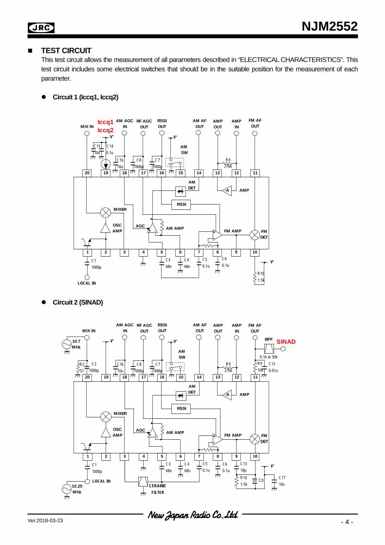
TEST CIRCUIT This test circuit allows the measurement of all parameters described in “ELECTRICAL CHARACTERISTICS”. This test circuit includes some electrical switches that should be in the suitable position for the measurement of each parameter. Circuit 1 (Iccq1, Iccq2)
Circuit 2 (SINAD)
CERAMICFILTER
V+
LOCAL IN
C11000p
C368n
C468n
C50.1u
C60.1u
C1318p
R101.5k
CD
C120.01u
R910k
V+
C71000p
C81000p
C1610u
C21000p
V+
R251
C1710u
MIX IN
10.7MHz
10.25MHz
SINADBPF
0.1k to 30k
AM AFOUT
AMPOUT
AMSW
RSSIOUT
RF AGCOUT
AMPIN
AM AGCIN
FM AFOUT
16 15 14 13 12 11
101 2 43 5 6 7 8
FM AMP FMDET
AMP
OSCAMP
MIXER
9
17181920
RSSI
-A
AM AMP
AMDET
AGC+ - +
-
R4270k
V+
LOCAL IN
C368n
C468n
C50.1u
C60.1u
R101.5k
R4270k
V+
C71000p
C81000p
C1610u
C1510u
C140.1u
V+
Iccq1Iccq2
AM SW
MIX INAM AF
OUTAMPOUT
RSSIOUT
RF AGCOUT
FM AFOUT
AMPIN
AM AGCIN
C11000p
16 15 14 13 12 11
101 2 43 5 6 7 8
FM AMP FMDET
AMP
OSCAMP
MIXER
9
17181920
RSSI
-A
AM AMP
AMDET
AGC+ - +
-

NJM2552
- 5 - Ver.2018-03-23
Circuit 3 (Gv)
Circuit 4 (Vod1/2, THD1/2/3, S/N1/2, AMR, Vrssi1/2/3, FMIFGV, VAGC, DVod )
V+
LOCAL IN
C368n
C468n
C50.1u
C60.1u
C1318p
R101.5k
C120.01u
R910k
R88.2k
C110.01u
V+
C71000p
C81000p
R320k
C1610u
V+
C1710u
MIX IN
51
Vod1THD1S/N1AMR
Vod2 DVodTHD2 S/N2THD3
450kHz
CD
FMIFGV
VAGC Vrssi
BPF
0.1k to 30k
AM AFOUT
AMPOUT
RSSIOUT
RF AGCOUT
FM AFOUT
AMPIN
AM AGCIN
C11000p
16 15 14 13 12 11
101 2 43 5 6 7 8
FM AMP FMDET
AMP
OSCAMP
MIXER
9
17181920
RSSI
-A
AM AMP
AMDET
AGC+ - +
-
LOCAL IN
C101u
R51kR4
270k
C91u
V+
MIX IN
FM AFOUT
Gv
31kHzV+
AM AFOUT
AMPOUT
AMSW
RSSIOUT
RF AGCOUT
AMPIN
AM AGCIN
C11000p
16 15 14 13 12 11
101 2 43 5 6 7 8
FM AMP FMDET
AMP
OSCAMP
MIXER
9
17181920
RSSI
-A
AM AMP
AMDET
AGC+ - +
-

NJM2552
- 6 - Ver.2018-03-23
Circuit 5 (Gmix)
CERAMICFILTER
LOCAL IN
C11000p
V+
C21000p
V+
R251
MIX IN10.7MHz
10.25MHz1.8k
Gmix
AM AFOUT
AMPOUT
AMSW
RSSIOUT
RF AGCOUT
FM AFOUT
AMPIN
AM AGCIN
16 15 14 13 12 11
101 2 43 5 6 7 8
FM AMP FMDET
AMP
OSCAMP
MIXER
9
17181920
RSSI
-A
AM AMP
AMDET
AGC+ - +
-

NJM2552
- 7 - Ver.2018-03-23
TERMINAL FUNCTION (Ta=25°C , V+=2.7V , circuit 1) Pin No. SYMBOL EQUIVARENT CIRCUIT VOLTAGE FUNCTION
1 OSC (B)
2.66V
Oscillator Base / Oscillator Emitter Colpitts - type oscillator is formed with an external oscillator element of crystal unit or SAW resonator. Output of an external oscillator circuit can also input to pin1 or pin2.
2 OSC (E) 1.95V
3 MIX OUT
1.75V
Mixer Output An external 450kHz ceramic filter is connected. The typical output impedance is 1.8kΩ.
4 GND - -- Ground
5 AM IF IN
1.35V
AM IF Input This is an AM IF signal input to AGC amplifier. The typical input impedance is 10kΩ.
6 AM DEC 1.35V
AM IF Decoupling This is an AM IF decoupling terminal for AGC amplifier. An external decoupling capacitor is connected to enhance stability.
7 FM IF IN
2.66V
IF Limiter Amplifier Input This is an input to the IF amplifier after passing through 450kHz ceramic filter. The typical input impedance is 1.8kΩ.
8 FM DEC 2.66V
IF Decoupling An external decoupling capacitor is connected to enhance stability.
1
2
22k
2k
170u
V+
GND
200k
1.4k
135u
320p
V+
GND
10k
1.24V
6
25u
5
V+
GND
8
7
51k
0.9k 0.9k
80u
2k
V+
GND

NJM2552
- 8 - Ver.2018-03-23
Pin No. SYMBOL EQUIVARENT CIRCUIT VOLTAGE FUNCTION
9 FM IF OUT
1.80V
FM IF Output This is an output of FM IF signal passing though the internal FM amplifier. An external phase - shifting capacitor is connected between pin9 and pin10.
10 QUAD IN
2.70V
Quadrature Detector Input An external phase - shifting coil or ceramic discriminator is connected.
11 FM AF OUT
0.96V
FM Demodulated Signal Output An external 3rd order multiple feed -back filter (RC filter) is connected.
12 AMP IN
0.66V
Input of Amplifier for Low Pass Filter External RC components form a low pass filter between pin12 and pin13. This terminal is biased from pin 11 though an external RC filter.
13 AMP OUT 0.71V
Output of Amplifier for Low Pass Filter
95u
9
V+
GND
20u
400
40010
V+
GND
95u
11
100k
10p
V+
GND
7.3k
1213
20u
V+
GND

NJM2552
- 9 - Ver.2018-03-23
Pin No. SYMBOL EQUIVARENT CIRCUIT VOLTAGE FUNCTION
14 AM AF OUT
1.46V
AM Demodulated Signal Output An external RC filter may be connected to reduce undesired signal.
15 AM SW
--
AM Section ON /OFF Switch Both of AM and FM section are in action during AM SW=HIGH. When AM SW=LOW, AM section keeps a state of not working.
16 RSSI OUT
0.17V
Received Signal Strength Indicator Output Pin 16 outputs DC level proportional to the log of input signal level to pin7.
17 RF AGC OUT
0.08V
Output of RF AGC circuit Pin 17 outputs DC voltage to control the gain of external RF amplifier.
100u
14
V+
GND
1550k
GND
55k
16
2k 2k 2k 2k
V+
GND
120k
2k
17
V+
GND

NJM2552
- 10 - Ver.2018-03-23
Pin No. SYMBOL EQUIVARENT CIRCUIT VOLTAGE FUNCTION
18 AM AGC IN
1.46V
Gain Control of AGC Circuit for AM Signal Pin 18 is connected with pin 14 through the external ripple filter of R and C.
19 V+ - - Supply Voltage
20 MIX IN
0.94V
Mixer Input The mixer is designed to work up to 100MHz with the typical input impedance of RinM = 3.6kΩ and CinM = 3.2pF(at 10.7MHz).
Note : 1. ESD protection diodes exist between each of the following pins and V+.
Pin 1,2,3,5,6,7,8,9,10,11,12,13,14,16,17,18,20 2. ESD protection diodes also exist between each of the following pins and ground.
Pin 1,2,3,5,6,7,8,9,10,11,12,13,14,15,16,17,18,20
25u
18
25u1.51
V+
GND
1k
3.6k
0.94
20
3.6k
25p
1k1k
50
V+
GND

NJM2552
- 11 - Ver.2018-03-23
EVALUATION PC BOARD The evaluation board is useful for your design and to have more understanding of the usage and performance of this device. This circuit is the same as TEST CIRCUIT. Note that this board is not prepared to show the recommendation of pattern and parts layout. Circuit Diagram
Note: 1. External Components
R1=R6=R7=0Ω R2=51Ω R3=20kΩ R4=270kΩ R5=1kΩ R8=8.2kΩ R9=10kΩ R10=1.5kΩ C1=C2=C7=1000pF C3=C4=68nF C5=C6=C14=0.1uF C9=C10=1uF C11=C12=0.01uF C13=18pF C15=C16=C17=10uF CD : Ceramic Discriminator, 450kHz CERAMIC FILTER : CF, 450kHz
CERAMICFILTER
V+
LOCAL IN
C11000p
C368n
C468n
C50.1u
C60.1u
C1318pR101.5k
CD
C120.01u
R910k
C101u
R51kR4
270k
C91u
R88.2k
C110.01u
V+
C71000p
C81000p
R320k
C1610u
C1510u
C140.1u
C21000p
V+
R251
C1710u
MIXIN
AM AFOUT
AMPOUT
RSSIOUT
RF AGCOUT
FM AFOUT
AMPIN
AM AGCIN
16 15 14 13 12 11
101 2 43 5 6 7 8
FM AMP FMDET
AMP
OSCAMP
MIXER
9
17181920
RSSI
-A
AM AMP
AMDET
AGC+ - +
-

NJM2552
- 12 - Ver.2018-03-23
Circuit Side View Ground Side View
CF
C17 +
C15+
C16
+
C14
R1
R2
R3
R4
R5 R6
R7
R8
R9
R10
C1
C2
C3C4
C5 C6
C8
C7
C9
C11
C12
C10
C13
CDN
JM2552
RF AGC OUT
RSSI OUT
OFF AM SWON
AM AF OUT
FM AF OUT
AMPIN
AMPOUT
V+GND
RF IN(MIX IN)
LOCAL IN(OSC(B))
NJM2552
V+
LOW
HIGH

NJM2552
- 13 - Ver.2018-03-23
1617181920MIX IN RF AGC
OUTV+
from IF Amp
V+V+
RF AGC Line
RF Amplifier
2k
127k
Tr2Tr3
Tr1
RF IN
Description AM AGC Line
1. Example of external circuit
2. Explanation AM AGC IN terminal (pin18) is usually connected with the AM DET terminal (pin 14) through the ripple filter of R3 and C16. This filter has the time constant of R3xC16 and this value of time constant is generally selected to be 5 to 10 times larger than the lowest cycle of the AM modulation signal (, not AM demodulated signal). AGC IN terminal (pin 18) can also be controlled by an external DC source instead of DC output of AM DET terminal.
RF AGC Line 1. Example of external circuit
2. Explanation RF AGC OUT terminal (pin17) can be connected to the bias circuit of the external RF amplifier to control its gain. RF AGC characteristics are shown on following page.
16 15 14 13 12 11
101 2 43 5 6 7 8
FM AMP FMDET
AMP
OSCAMP
MIXER
9
17181920
RSSI
-A
AM AMP
AMDET
AGC+-
+ -
CERAMICFILTER
R320k
C1610u
AGC IN
AM AFOUT
FM AFOUT
+
AM AGC Line
AM IF
V+
V+
V+
120k
NJM2552
- 14 - Ver.2018-03-23
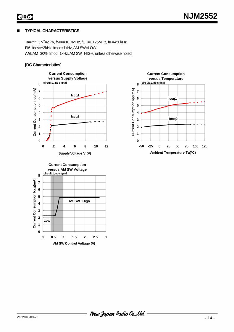
TYPICAL CHARACTERISTICS Ta=25°C, V+=2.7V, fMIX=10.7MHz, fLO=10.25MHz, fIF=450kHz FM: fdev=±3kHz, fmod=1kHz, AM SW=LOW AM: AM=30%, fmod=1kHz, AM SW=HIGH, unless otherwise noted. [DC Characteristics]
Current Consumptionversus Temperature
0
1
2
3
4
5
6
7
8
-50 -25 0 25 50 75 100 125
Ambient Temperature Ta(°C)
Cur
rent
Con
sum
ptio
n Iq
q(m
A)
Iccq1
Iccq2
circuit 1, no signal
Current Consumptionversus AM SW Voltage
0
1
2
3
4
5
6
7
8
0 0.5 1 1.5 2 2.5 3
AM SW Control Voltage (V)
Cur
rent
Con
sum
ptio
n Ic
cq(m
A)
Low
AM SW : High
circuit 1, no signal
Current Consumptionversus Supply Voltage
0
1
2
3
4
5
6
7
8
0 2 4 6 8 10 12
Supply Voltage V+(V)
Cur
rent
Con
sum
ptio
n Iq
q(m
A)
Iccq1
Iccq2
circuit 1, no signal

NJM2552
- 15 - Ver.2018-03-23
[Mixer Characteristics]
Mixer Conversion Gain versusFrequency and Supply Voltage
10
15
20
25
30
10 100 1000
Mixer Input Frequency fMIX(MHz)
Mix
er C
onve
rsio
n G
ain
Gm
ix(d
B)
circuit 5, VinMIX=40dBuV, VinLO=100dBuV
V+=2.2V
V+=9V
V+=2.7V
Mixer Conversion Gain versusFrequency and Temperature
10
15
20
25
30
10 100 1000
Mixer Input Frequency fMIX(MHz)
Mix
er C
onve
rsio
n G
ain
Gm
ix(d
B)
Ta=85°C
Ta=25°C
Ta=- 40°C
circuit 5 , VinMIX=40dBuV , VinLO=100dBuV
Mixer 3rd Order Intermodulation
0
20
40
60
80
100
120
0 20 40 60 80 100 120
Mixer Input Level VinMIX(dBuV)
Mix
er O
utpu
t Lev
el (d
BuV
)
Desired Products
3rd OrderIntermod.Products
IIP3
1dB Comp.Pt.
circuit 5, VinLO=100dBuV
Mixer Conversion Gain vesus Local Input Level
0
5
10
15
20
25
40 60 80 100 120
Local Input Level VinLO(dBuV)
Mix
er C
onve
rsio
n G
ain
Gm
ix(d
B)
circuit 5, VinMIX=40dBuV
Ta=85°C
Ta= 25°C
Ta=- 40°C

NJM2552
- 16 - Ver.2018-03-23
[RSSI Characteristics]
RSSI Output versus Mixer Inputand Ambient Temperature
0
0.5
1
1.5
2
2.5
3
-20 0 20 40 60 80 100 120
Mixer Input Level VinMIX(dBuV)
RSS
I Out
put V
olta
ge V
rssi
(V)
- 40°C
circuit 2 , VinLO=100dBuV
Ta=85°C, 25°C
RSSi Output versus IF Inputand Ambient Temperature
0
0.5
1
1.5
2
2.5
3
-20 0 20 40 60 80 100 120
IF Input Level VinIF(dBuV)
RSS
I Out
put V
olta
ge V
rssi
(V)
circuit 4
Ta=85°C, 25°C
- 40°C
RSSI Output versus Temperatureand IF Input Level
0
0.5
1
1.5
2
2.5
3
-50 -25 0 25 50 75 100 125
Ambient Temperature Ta(°C)
RSS
I Out
put V
olta
ge V
rssi
(V)
100dBuV
circuit 4
VinMIX=120dBuV90dBuV
80dBuV
70dBuV
60dBuV
50dBuV
40dBuV
- 20dBuV
RSSI Output versus IF Inputand Supply Voltage
0
0.5
1
1.5
2
2.5
3
-20 0 20 40 60 80 100 120
IF Input Level VinIF(dBuV)
RSS
I Out
put V
olta
ge V
rssi
(V)
2.2V
V+= 9V
2.7V
circuit 4
RSSI Output versus Mixer Inputand Supply Voltage
0
0.5
1
1.5
2
2.5
3
-20 0 20 40 60 80 100 120
Mixer Input Level VinMIX(dBuV)
RSS
I Out
put V
olta
ge V
rssi
(dB
)
V+=2.2V
V+= 9V
V+=2.7V
circuit 2 , VinLO=100dBuV

NJM2552
- 17 - Ver.2018-03-23
[RF AGC Characteristics]
RF AGC Output versus IF Inputand Ambient Temperature
00.20.40.60.8
11.21.41.61.8
22.22.4
-20 0 20 40 60 80 100 120
IF Input Level VinIF(dBuV)
RF A
GC
Out
put V
olta
ge V
AGC(
V)
Ta=85°C, 25°C, - 40°C
circuit 4
RF AGC Output versus Temperatureand IF Input Level
00.20.40.60.8
11.21.41.61.8
2
-50 -25 0 25 50 75 100 125
Ambient Temperature Ta(°C)
RF A
GC
Out
put V
olta
ge V
AGC(
V) VinMIX=120dBuV90dBuV85dBuV
80dBuV
75dBuV
70dBuV
- 20dBuV
circuit 4
RF AGC Output versus Mixer Inputand Supply Voltage
00.20.40.60.8
11.21.41.61.8
22.22.4
-20 0 20 40 60 80 100 120
Mixer Input Level VinMIX(dBuV)
RF
AG
C O
utpu
t Vol
tage
(V) V+=9.0V
2.7V
2.2V
circuit 2 , VinLO=100dBuV
RF AGC Output versus IF Inputand Supply Voltage
00.20.40.60.8
11.21.41.61.8
22.22.4
0 20 40 60 80 100 120
IF Input Level VinIF(dBuV)
RF A
GC
Out
put V
olta
ge V
AGC(
V)
V+=9.0V
2.7V
2.2V
circuit 4
RF AGC Output versus Mixer Inputand Ambient Temperature
00.20.40.60.8
11.21.41.61.8
22.22.4
-20 0 20 40 60 80 100 120
Mixer Input Level VinMIX(dBuV)
RF
AG
C O
utpu
t Vol
tage
(V)
circuit 2 , VinLO=100dBuV
Ta=85°C, 25°C, - 40°C

NJM2552
- 18 - Ver.2018-03-23
[FM Demodulation Characteristics]
FM Demod.Output and Distortion-IF Detuning Characteristics-
0.1
1
10
100
1000
430 440 450 460 470
IF Input Frequency fIF(kHz)
FM D
emod
ulat
ed O
utpu
tLe
vel1
Vod
1(m
Vrm
s)
0.1
1
10
100
1000
Dis
tort
ion
THD
1(%
)
Vod1
THD1
circuit 4 , VinIF=80dBuV
FM AF OUT Voltage versus Frequencyand Ambient Temperature (S-Curve)
0
0.5
1
1.5
2
2.5
420 430 440 450 460 470 480
IF Input Frequency fIF(kHz)
FM A
F O
UT
Volta
ge(V
)
Ta=85°C
Ta= 25°C
Ta=- 40°C
circuit 4 , VinIF=80dBuV
FM AF OUT Voltage versus Frequencyand Supply Voltage (S-Curve)
0
0.5
1
1.5
2
2.5
420 430 440 450 460 470 480
IF Input Frequency fIF(kHz)
FM A
F O
UT
Volta
ge(V
)
V+=9.0V
V+=2.7V2.2V
circuit 4 , VinIF=80dBuV
FM Demod. Output versusFM Modulation Frequency
020406080
100120140160180200
0.1 1 10 100
FM Modulation Frequency fmod(kHz)
FM D
emod
ulat
ed O
utpu
tLe
vel1
Vod
1(m
Vrm
s)
circuit 4, VinIF=80dBuV
FM : S+N, N, AMR, SINAD, THD1versus Mixer Input Level
-70
-60
-50
-40
-30
-20
-10
0
10
-20 0 20 40 60 80 100 120
Mixer Input Level VinMIX(dBuV)
S+N
, N, A
MR
(dB
)
0
10
20
30
40
50
60
70
80
SIN
AD
(dB
), TH
D1(
%)
S+N
SINAD
AMR
NTHD1
circuit 2 , VinLO=100dBuV
FM : S+N, N, AMR, SINAD, THD1versus IF Input Level
-70
-60
-50
-40
-30
-20
-10
0
10
-20 0 20 40 60 80 100 120
IF Input Level VinIF(dBuV)
S+N
, N, A
MR
(dB
)
0
10
20
30
40
50
60
70
80
SIN
AD
(dB
), TH
D1(
%)
S+N
SINAD
AMR
N
THD1
circuit4

NJM2552
- 19 - Ver.2018-03-23
[AM Demodulation Characteristics]
AM30% : S+N, N versusIF Input Level
-70
-60
-50
-40
-30
-20
-10
0
10
-20 0 20 40 60 80 100 120
IF Input Level VinIF(dBuV)
S+N
, N (d
B)
S+N
N
circuit4 , AM=30%
AM30%: Demodulated Output Levelversus Ambient Temperature
40
45
50
55
60
65
70
75
80
85
-50 -25 0 25 50 75 100 125
Ambient Temperature Ta(°C)
AM
Dem
odul
ated
Out
put
Leve
l Vod
2(m
Vrm
s)
circuit4, VinIF=80dBuV, AM=30%
AM30% : Demod. Output and Distortionversus IF Input Level
0.1
1
10
100
1000
-20 0 20 40 60 80 100 120
IF Input Level VinIF(dBuV)AM
Dem
odul
ated
Out
put
Leve
l Vod
2(m
Vrm
s)
0.1
1
10
100
1000
Dis
tort
ion
THD
2(%
)Vod2
THD2
circuit4, AM=30%
AM30% : S+N, N versusMixer Input Level
-70
-60
-50
-40
-30
-20
-10
0
10
-20 0 20 40 60 80 100 120
Mixer Input Level VinMIX(dBuV)
S+N
, N (d
B)
S+N
N
circuit 2 , VinLO=100dBuV , AM=30%
AM30%: Demodulated Output Levelversus Supply Voltage
40
45
50
55
60
65
70
75
80
85
2 4 6 8 10 12
Supply Voltage V+(V)
AM
Dem
odul
ated
Out
put
Leve
l Vod
2(m
Vrm
s)
circuit 4 , VinIF=80dBuV , AM=30%
AM30% : Demod. Output and Distortionversus Mixer Input Level
0.1
1
10
100
1000
-20 0 20 40 60 80 100 120
Mixer Input Level VinMIX(dBuV)
AM D
emod
ulat
ed O
utpu
tLe
vel V
od2(
mVr
ms)
0.1
1
10
100
1000
Dis
tort
ion
THD
2(%
)Vod2
THD2
circuit 2 , VinLO=100dBuV , AM=30%

NJM2552
- 20 - Ver.2018-03-23
AM80% : Demod. Output and Distortionversus Mixer Input Level
0.1
1
10
100
1000
-20 0 20 40 60 80 100 120
Mixer Input Level VinMIX(dBuV)
AM
Dem
odul
ated
Out
put
Leve
l Vod
2(m
Vrm
s)
0.1
1
10
100
1000
Dis
tort
ion
THD
3(%
)
Vod2
THD3
circuit 2 , VinLO=100dBuV , AM=80%
AM Demodulated Output versusIF Input Frequency
0102030405060708090
100
0.1 1 10 100
IF Input Frequency fIF(MHz)
AM
Dem
odul
ated
Out
put
Leve
l Vod
2(m
Vrm
s)
circuit4, VinIF=80dBuV, AM=30%
fif=450kHz
AM80% : Demod. Output and Distortionversus IF Input Level
0.1
1
10
100
1000
-20 0 20 40 60 80 100 120
IF Input Level VinIF(dBuV)
AM D
emod
ulat
ed O
utpu
tLe
vel V
od2(
mVr
ms)
0.1
1
10
100
1000
Dis
tort
ion
THD
3(%
)
Vod2
THD3
circuit4, AM=80%
AM80% : S+N, N versusIF Input Level
-70
-60
-50
-40
-30
-20
-10
0
10
-20 0 20 40 60 80 100 120
IF Input Level VinIF(dBuV)
S+N
, N (d
B)
S+N
N
circui4 , AM=80%
AM Demodulated Output versusAM Modulation Frequency
0102030405060708090
100
0.1 1 10 100
AM Modulation Frequency fmod(kHz)
AM
Dem
odul
ated
Out
put
Leve
l Vod
2(m
Vrm
s)
circuit4(BPF less), VinIF=80dBuV, AM=30%
AM80% : S+N, N versusMixer Input Level
-70
-60
-50
-40
-30
-20
-10
0
10
-20 0 20 40 60 80 100 120
Mixer Input Level VinMIX(dBuV)
S+N
, N (d
B)
circuit 2 , VinLO=100dBuV, AM=80%
S+N
N

NJM2552
- 21 - Ver.2018-03-23
[CAUTION] The specifications on this databook are only
given for information , without any guarantee as regards either mistakes or omissions. The application circuits in this databook are described only to show representative usages of the product and not intended for the guarantee or permission of any right including the industrial rights.