Embed Size (px)
Citation preview

IEEE 100BASE-T1 EMC Test Specification for ESD suppression devices
Version 2.0
Author & Company Dr. Bernd Körber, FTZ Zwickau
Title 100BASE-T1 EMC Test Specification for ESD suppression devices
Version 2.0
Date October 30, 2020
Status Final
Restriction Level Public
This measurement specification shall be used as a standardized common scale for EMC evaluation of ESD suppression devices for 100BASE-T1 in automotive applications.
OPEN Alliance
Restriction Level: Public | 100BASE-T1 EMC Test Specification for ESD Suppression Devices | Oct-20 2
Version Control of Document
Version Author Description Date
0.1 B. Körber Initial version 07/05/17
1.0 B. Körber Shift to final version 10/29/17
2.0_Draft1 B. Körber Adaptations to 1000BASE-T1 EMC Test Specification for ESD Suppression Devices and IEC 62228-5 draft version
01/25/20
2.0_Draft2 B. Körber Editorial changes 03/16/20
2.0 B. Körber Shift to final version 30/10/20
Restriction level history of Document
Version Restriction Level Description Date
0.1 Open internal only 07/05/17
1.0 Public 10/29/17
2.0_Draft1 Open internal only 01/25/20
2.0_Draft2 Open internal only 03/16/20
2.0 Public 30/10/20

OPEN Alliance
Restriction Level: Public | 100BASE-T1 EMC Test Specification for ESD Suppression Devices | Oct-20 3
Copyright Notice and Disclaimer
OPEN Alliance members whose contributions were incorporated in the OPEN Specification (the “Contributing Members”) own the copyrights in the OPEN Specification, and permit the use of this OPEN Specification, including the copying and distribution of unmodified copies thereof, for informational purposes only. Such permission relates only to the OPEN Specification and does not include a specification published elsewhere and referred to in the OPEN Specification.
The receipt of an OPEN Specification shall not operate as an assignment or license under any patent, industrial design, trademark, or other rights as may subsist in or be contained in or reproduced in any OPEN Specification, and the implementation of this OPEN Specification will require such a license.
THIS OPEN SPECIFICATION IS PROVIDED ON AN “AS IS” BASIS AND ALL WARRANTIES, EITHER EXPLICIT OR IMPLIED, ARE EXCLUDED UNLESS MANDATORY UNDER LAW. ACCORDINGLY, THE OPEN ALLIANCE AND THE CONTRIBUTING MEMBERS MAKE NO REPRESENTATIONS OR WARRANTIES WITH REGARD TO THE OPEN SPECIFICATION OR THE INFORMATION (INCLUDING ANY SOFTWARE) CONTAINED THEREIN, INCLUDING ANY WARRANTIES OF MERCHANTABILITY, FITNESS FOR PURPOSE, OR ABSENCE OF THIRD PARTY RIGHTS AND MAKE NO REPRESENTATIONS AS TO THE ACCURACY OR COMPLETENESS OF THE OPEN SPECIFICATION OR ANY INFORMATION CONTAINED THEREIN.
THE OPEN ALLIANCE AND CONTRIBUTING MEMBERS ARE NOT LIABLE FOR ANY LOSSES, COSTS, EXPENSES OR DAMAGES ARISING IN ANY WAY OUT OF USE OR RELIANCE UPON THE OPEN SPECIFICATION OR ANY INFORMATION THEREIN. NOTHING IN THIS DOCUMENT OPERATES TO LIMIT OR EXCLUDE ANY LIABILITY FOR FRAUD OR ANY OTHER LIABILITY WHICH IS NOT PERMITTED TO BE EXCLUDED OR LIMITED BY OPERATION OF LAW.
Without prejudice to the foregoing, the OPEN Specification was developed for automotive applications only. The OPEN Specification has neither been developed, nor tested for non-automotive applications.
OPEN Alliance reserves the right to withdraw, modify, or replace the OPEN Specification at any time, without notice.
OPEN Alliance
Restriction Level: Public | 100BASE-T1 EMC Test Specification for ESD Suppression Devices | Oct-20 4
Contents 1 Introduction .................................................................................................................................... 5
1.1 Scope ....................................................................................................................................... 5
1.2 References ............................................................................................................................... 5
1.3 List of Abbreviations and Definitions ........................................................................................ 6
2 General Definitions and Requirements for ESD Suppression Devices ................................................ 7
2.1 Arrangement of ESD Suppression Device within 100BASE-T1 MDI network .............................. 7
2.2 Evaluation of Datasheet Parameters ........................................................................................ 8
3 Required Tests ................................................................................................................................. 9
3.1 General .................................................................................................................................... 9
3.2 Mixed Mode S-Parameter Measurement................................................................................ 10
3.2.1 Test setup....................................................................................................................... 10
3.2.2 Test procedure and parameters ...................................................................................... 11
3.3 Damage from ESD .................................................................................................................. 13
3.3.1 Test setup....................................................................................................................... 13
3.3.2 Test procedure and parameters ...................................................................................... 14
3.4 ESD discharge current measurement ...................................................................................... 16
3.4.1 Test setup....................................................................................................................... 16
3.4.2 Test procedure and parameters ...................................................................................... 17
3.5 Test of unwanted Clamping Effect at RF immunity Tests ......................................................... 19
3.5.1 Test setup....................................................................................................................... 19
3.5.2 Test procedure and parameters ...................................................................................... 20
Appendix A - Test Circuit Boards ............................................................................................................ 22
A.1 General requirements for test fixtures ................................................................................... 22
A.2 Self-balance requirements for S-Parameter test fixture .......................................................... 22
A.3 Example for test fixture S-Parameter measurement ............................................................... 24
A.4 Example for test fixture ESD tests ........................................................................................... 25
A.5 Example for Test Fixture ESD Discharge Current Measurement .............................................. 25
Appendix B – Recommended Limits for Tests ........................................................................................ 26
B.1 S-Parameter Measurements ................................................................................................... 26
B.2 Damage from ESD .................................................................................................................. 28
B.3 ESD Discharge Current Measurement ..................................................................................... 28
B.4 Test of unwanted Clamping Effect at RF Immunity Tests......................................................... 30
OPEN Alliance
Restriction Level: Public | 100BASE-T1 EMC Test Specification for ESD Suppression Devices | Oct-20 5
1 Introduction
1.1 Scope
ESD suppression devices can be used to increase the ESD robustness of 1000BASE-T1 Ethernet
transceivers according to [IEEE1] and can have a significant effect on EMC test results in communication
networks. In principle there are two possible positions of ESD suppression device implementation within
an Ethernet interface: between the transceiver and the CMC or between the MDI connector and the
common mode termination network as described in Figure 2-1.
This measurement specification shall be used as a standardized common scale for EMC evaluation of ESD
suppression devices intended to use for position between MDI connector and common mode termination
network within the 100BASE-T1 interface. It contains recommended limits. The final judgment of the
tested device is left to the customer.
This instruction includes test procedures and test setups concerning:
evaluation of datasheet parameters
mixed mode S-Parameter measurement
test of damage from ESD
test of unwanted clamping effect at RF immunity tests
impact to ESD discharge current in a defined 100BASE-T1 network.
It shall be used for evaluation of ESD suppression devices or passive components with internal ESD
suppression unit (e.g. combination of ESD suppression and common mode termination circuit).
1.2 References
[IEEE1] IEEE Std. 802.3bw
[IEC1] IEC 62615, Electrostatic discharge sensitivity testing - Transmission line pulse (TLP) - Component level
[ISO1] ISO 10605, Road vehicles – Test methods for electrical disturbances from electrostatic discharge
[OPEN1] OPEN ALLIANCE, IEEE 100BASE-T1 EMC Test Specification for Common mode chokes
[OPEN2] OPEN ALLIANCE, IEEE 100BASE-T1 EMC Test Specification for Transceivers
OPEN Alliance
Restriction Level: Public | 100BASE-T1 EMC Test Specification for ESD Suppression Devices | Oct-20 6
1.3 List of Abbreviations and Definitions
BIN Bus Interface Network
CMC Common Mode Choke
CMR Common Mode Rejection
DCMR Differential to Common Mode Rejection, common mode single ended measured
ESD Electro Static Discharge
IL Insertion Loss
MDI Medium Dependent Interface
RF Radio Frequency
RL Return Loss
S-Parameter Scattering Parameter
VNA Vector Network Analyzer
OPEN Alliance
Restriction Level: Public | 100BASE-T1 EMC Test Specification for ESD Suppression Devices | Oct-20 7
2 General Definitions and Requirements for ESD Suppression Devices
2.1 Arrangement of ESD Suppression Device within 100BASE-T1 MDI
network
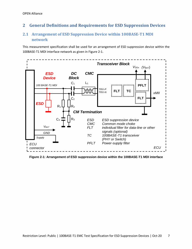
This measurement specification shall be used for an arrangement of ESD suppression device within the
100BASE-T1 MDI interface network as given in Figure 2-1.
ECU connector
VDDx
TRX-P TRX-N
C1
C2
L1
C3
R2 R1
ECU
DC Block
CM Termination
CMC
100 BASE-T1 MDI
Supply
FLT TC
PFLT
FLT
Transceiver Block
xMII
(VBAT)
ESD ESD suppression device CMC Common mode choke FLT individual filter for data-line or other
signals (optional) TC 100BASE-T1 transceiver (PHY or Switch)
PFLT Power-supply filter xMII MII, RGMII or SGMII (MAC interface)
ESD Device
R3
ESD
VBAT
GND
Figure 2-1: Arrangement of ESD suppression device within the 100BASE-T1 MDI interface

OPEN Alliance
Restriction Level: Public | 100BASE-T1 EMC Test Specification for ESD Suppression Devices | Oct-20 8
2.2 Evaluation of Datasheet Parameters
The following parameters for ESD suppression device shall be ensured and documented in the datasheet.
Parameter Target Value
Working direction bi-directional
Operation voltage (VDCmax) ≥ 24 V
ESD trigger voltage ≥ 100 V
ESD robustness +/- 15kV contact discharge for unpowered device using discharge
module according to ISO 10605 (discharge storage capacitor C =
150 pF and discharge resistor R = 330 )
Minimum number of discharges > 1000
TLP characteristic according to
[IEC1]
I/V characteristics
Table 2-1: Target values for ESD suppression device
The given target values for operation voltage and ESD trigger voltage are related to the position of ESD
protection device within the BIN as given in Figure 2-1.

OPEN Alliance
Restriction Level: Public | 100BASE-T1 EMC Test Specification for ESD Suppression Devices | Oct-20 9
3 Required Tests
3.1 General
For evaluation of EMC behavior of the ESD suppression device the following tests are defined:
mixed mode S-Parameter measurement
test of damage from ESD
impact to ESD discharge current in a defined 100BASE-T1 network
test of unwanted clamping effect at RF immunity tests.
All test are defined at a two-line ESD suppression device used in a 100BASE-T1 MDI. If the ESD suppression
device has more than two lines the test setup should be adapted accordingly. For single devices the test
should be performed with a combination of two devices of the same type.
Prior to performing any RF and ESD tests, the S-Parameter measurements shall be performed on a
minimum of 10 samples.
OPEN Alliance
Restriction Level: Public | 100BASE-T1 EMC Test Specification for ESD Suppression Devices | Oct-20 10
3.2 Mixed Mode S-Parameter Measurement
3.2.1 Test setup
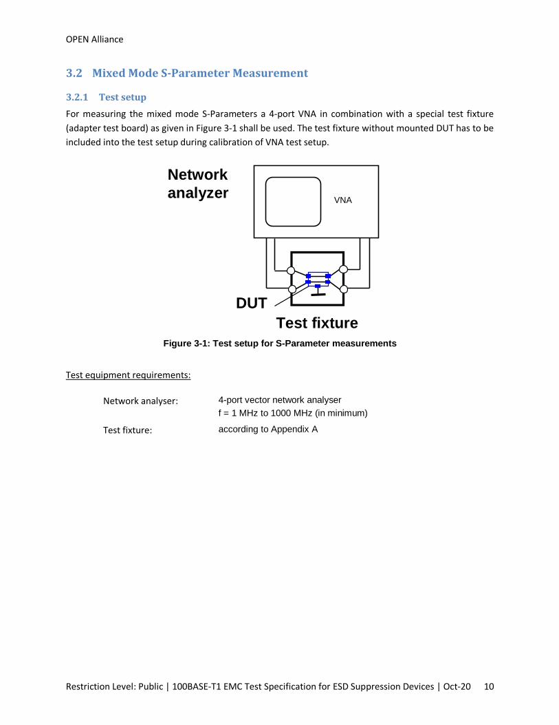
For measuring the mixed mode S-Parameters a 4-port VNA in combination with a special test fixture
(adapter test board) as given in Figure 3-1 shall be used. The test fixture without mounted DUT has to be
included into the test setup during calibration of VNA test setup.
VNA
Test fixture
Network
analyzer
DUT
Figure 3-1: Test setup for S-Parameter measurements
Test equipment requirements:
Network analyser: 4-port vector network analyser
f = 1 MHz to 1000 MHz (in minimum)
Test fixture: according to Appendix A

OPEN Alliance
Restriction Level: Public | 100BASE-T1 EMC Test Specification for ESD Suppression Devices | Oct-20 11
3.2.2 Test procedure and parameters
The test procedure and parameter for S-Parameter measurements are defined in Table 3-1.
Parameter Description
Frequency range: 1 MHz to 1 GHz, logarithmic scale
S-Parameter per
single path:
Sdd11 (RL), log. magnitude in dB / transceiver side
Sdd21 (IL), log. magnitude in dB
Ssd21 (DCMR), log. magnitude in dB / transceiver side
VNA measurement
circuit:
Port definitions:
Mixed mode logic port 1: physical port 1a and port 1b / transceiver side
Mixed mode logic port 2: physical port 2a and port 2b / connector side
Pin 1 of DUT is placed on transceiver side (logic port 1).
Sdd11 and Sdd21 measurement:
50 Ω input impedance at each measurement port
VNA port 1a
(50 Ohm)
VNA port 1b
(50 Ohm)
DUT
VNA port 2a
(50 Ohm)
VNA port 2b
(50 Ohm)
1
Logical
port 1
Logical
port 2
GND
Ssd21 measurement:
Differential mode input (logical port 1): 50 Ω impedance each
Common mode output (logical port 2):
symmetrical single ended network with 200 Ω impedance
R = R1||R2 + R3 + RVNA port 2a
Single ended VNA port 2a
(50 Ohm)
124
49.9
49.9
DUT
1
VNA port 1a
(50 Ohm)
VNA port 1b
(50 Ohm)
Logical
port 1
Logical
port 2
R1
R2
R3
GND
Note: The accuracy of resistor values should be 1 %. The difference
between matching resistors should be 0.1 %.
Table 3-1: Test parameters for S- Parameter measurements
OPEN Alliance
Restriction Level: Public | 100BASE-T1 EMC Test Specification for ESD Suppression Devices | Oct-20 12
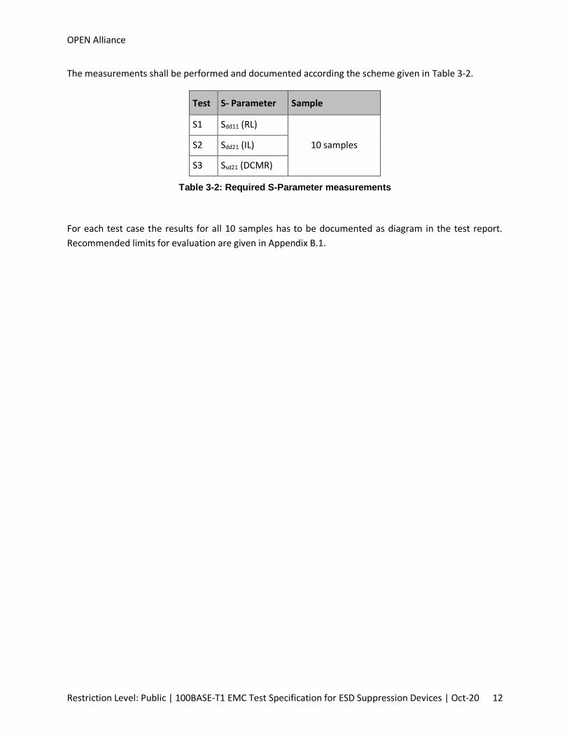
The measurements shall be performed and documented according the scheme given in Table 3-2.
Test S- Parameter Sample
S1 Sdd11 (RL)
10 samples S2 Sdd21 (IL)
S3 Ssd21 (DCMR)
Table 3-2: Required S-Parameter measurements
For each test case the results for all 10 samples has to be documented as diagram in the test report.
Recommended limits for evaluation are given in Appendix B.1.

OPEN Alliance
Restriction Level: Public | 100BASE-T1 EMC Test Specification for ESD Suppression Devices | Oct-20 13
3.3 Damage from ESD
3.3.1 Test setup
The setup given in Figure 3-2 shall be used for testing the ESD robustness of ESD suppression device.
ESD Test board
GND Discharge points
DP1, DP2
Ground plane ESD Test board
Connection point
Ground plane
Test generator with contact
discharge module
ESD Simulator
Ground reverse line
Test generator
Ground plane (minimal 0.5 m x 0.5 m)
ESD Test board
fixture
Surface connection ESD Test board to Test
board support
Surface connection
Test board fixture to
ground plane
ESD suppression
device
Figure 3-2: Test setup for ESD damage tests
The ground plane with a minimum size of 0.5 m x 0.5 m builds the reference ground plane for the ESD
Test setup and must be connected with the electrical grounding system of the test laboratory. The ESD
Test generator ground cable shall be connected to this reference plane. The test board fixture realizes the
positioning of the ESD Test board and the electrical connection of the ESD Test board ground plane with
the reference ground plane. This connection must have low impedance (R < 25 m) and should be built
by a surface contact.
During testing the tip of the ESD Test generator discharge module shall be directly contacted with one of
the discharge pads DP1 or DP2 of the ESD test board. For this purpose, the discharge points DP1 and DP2
are implemented as rounded vias in the layout of the ESD test board and are directly connected by a trace
15 (-0 +5) mm with the respective pin of the ESD suppression device.
Test Equipment Requirements:
ESD test generator: according to [ISO1]; contact discharge module with
discharge capacitor 150 pF and discharge resistor
330
ESD test board: according to Appendix A
OPEN Alliance
Restriction Level: Public | 100BASE-T1 EMC Test Specification for ESD Suppression Devices | Oct-20 14
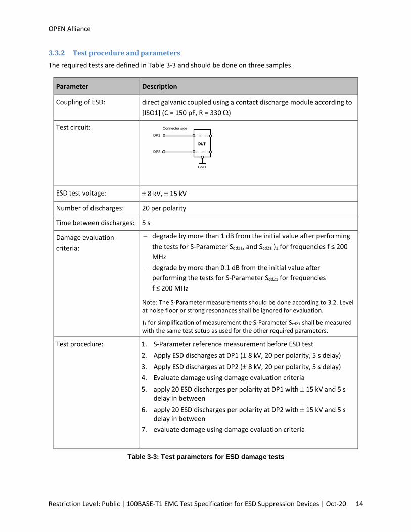
3.3.2 Test procedure and parameters
The required tests are defined in Table 3-3 and should be done on three samples.
Parameter Description
Coupling of ESD: direct galvanic coupled using a contact discharge module according to
[ISO1] (C = 150 pF, R = 330 )
Test circuit:
DUT
DP1
Connector side
GND
DP2
ESD test voltage: 8 kV, 15 kV
Number of discharges: 20 per polarity
Time between discharges: 5 s
Damage evaluation
criteria:
degrade by more than 1 dB from the initial value after performing
the tests for S-Parameter Sdd11, and Scd21 )1 for frequencies f ≤ 200
MHz
degrade by more than 0.1 dB from the initial value after
performing the tests for S-Parameter Sdd21 for frequencies
f ≤ 200 MHz
Note: The S-Parameter measurements should be done according to 3.2. Level at noise floor or strong resonances shall be ignored for evaluation.
)1 for simplification of measurement the S-Parameter Scd21 shall be measured with the same test setup as used for the other required parameters.
Test procedure: 1. S-Parameter reference measurement before ESD test
2. Apply ESD discharges at DP1 ( 8 kV, 20 per polarity, 5 s delay)
3. Apply ESD discharges at DP2 ( 8 kV, 20 per polarity, 5 s delay)
4. Evaluate damage using damage evaluation criteria
5. apply 20 ESD discharges per polarity at DP1 with 15 kV and 5 s delay in between
6. apply 20 ESD discharges per polarity at DP2 with 15 kV and 5 s delay in between
7. evaluate damage using damage evaluation criteria
Table 3-3: Test parameters for ESD damage tests

OPEN Alliance
Restriction Level: Public | 100BASE-T1 EMC Test Specification for ESD Suppression Devices | Oct-20 15
The tests shall be performed and documented according the scheme given in Table 3-4.
Test Discharge points
Comment Sample
E1 DP1 Line 1 3 samples
E2 DP2 Line 2
Table 3-4: Required ESD tests for damage
Recommended limits for ESD test voltages are given in Appendix B.2.

OPEN Alliance
Restriction Level: Public | 100BASE-T1 EMC Test Specification for ESD Suppression Devices | Oct-20 16
3.4 ESD discharge current measurement
3.4.1 Test setup
The setup given in Figure 3-3 shall be used for measuring the ESD discharge current through a 100BASE-
T1 transceiver simulation network if the ESD suppression device is used as a part of the MDI network.
ESD Test board
GND
Discharge points
DP1, DP2
Ground plane ESD Test board
Connection point
Ground plane
Test generator with contact
discharge module
ESD Simulator
Ground reverse line
Test generator
Ground plane (minimal 0.5 m x 0.5 m)
ESD Test board
fixture
Surface connection ESD Test board to Test
board support
Surface connection
Test board fixture to
ground plane
RF Coax
connector MDI test network with
DUT
RF Coax connector DSO
50Ω 50Ω
Measurement
equipment
RF attenuator
(50 )
Figure 3-3: Test setup for ESD discharge current measurement
The ground plane with a minimum size of 0.5 m x 0.5 m builds the reference ground plane for the ESD
Test setup and must be connected with the electrical grounding system of the test laboratory. The ESD
Test generator ground cable shall be connected to this reference plane. The test board fixture realizes the
positioning of the ESD Test board and the electrical connection of the ESD Test board ground plane with
the reference ground plane. This connection must have low impedance (R < 25 m) and should be built
by a surface contact. Copper tapes can be used in addition. For reduction of parasitic field coupling from
ESD generator into the test circuit it is recommended to position the ESD test board with passive
components on bottom side into the metallic test fixture.
During testing the tip of the ESD Test generator discharge module shall be directly contacted with one of
the discharge pads DP1 or DP2 of the ESD test board. For this purpose, the discharge points DP1 and DP2
are implemented as rounded vias in the layout of the ESD test board and are directly connected by a trace
15 (-0 +5) mm with the MDI test network.
Shielded cables are used for connection of measurement outputs of the MDI test network on the ESD test
board to the DSO with 50Ω input impedance. An additional attenuator prevents the DSO inputs from
damage. Care should be taken that the used DSO is not influenced by the ESD discharge event.

OPEN Alliance
Restriction Level: Public | 100BASE-T1 EMC Test Specification for ESD Suppression Devices | Oct-20 17
Test Equipment Requirements:
ESD test generator: according to [ISO1]; contact discharge module with discharge
capacitor 150 pF and discharge resistor 330
DSO 50 Ω input impedance, minimum 1GHz analog input bandwidth
RF attenuator 50 Ω input impedance, minimum 10 dB attenuation
ESD test board: according to Appendix A
3.4.2 Test procedure and parameters
The required tests are defined in Table 3-5 and should be done on three samples.
Parameter Description
Coupling of ESD: direct galvanic coupled using a contact discharge module according to
[ISO] (C = 150 pF, R = 330 )
Test circuit:
DUT
ESD
Test port
ESD device
1k (1%) 1k (1%)
10k
4.7nF
CMC
(200µH)
100BASE-T1 Transceiver Simulation network
100nF
DP1
DP2
2 2 50 50
ESD Test board DSO
50
100nF 50
RF Coax
connector
MDI test network
1
Note: The used CMC should fulfil the requirements of [OPEN1]. If available, a
representing CMC for each CMC ESD saturation class I and II should be used
for testing.
The resistors for common mode termination network shall be from the SMD
design 1206 or 0805 with a maximum tolerance of 1 %. The exact type ID and
manufacturer of the used resistors must be documented in the test report.
The resistors for transceiver simulation network shall be SMD types design
0603 or 0402. A parallel circuit of resistors is recommended to achieve low
impedance of network.
ESD test voltage: 3 kV, 5 kV, 6 kV, 7 kV, 15 kV
Evaluation criteria: measured ESD discharge current waveform
Table 3-5: Test parameters for ESD discharge current measurement
The tests shall be performed and documented according the scheme given in Table 3-6.
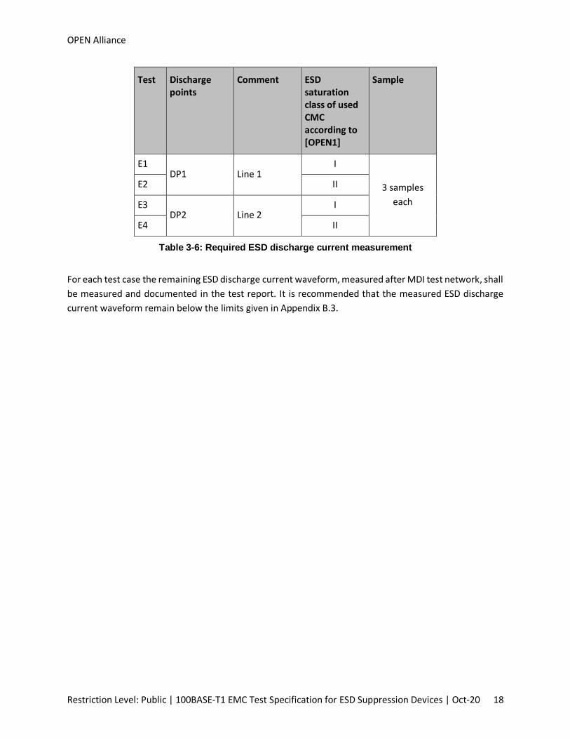
OPEN Alliance
Restriction Level: Public | 100BASE-T1 EMC Test Specification for ESD Suppression Devices | Oct-20 18
Test Discharge points
Comment ESD saturation class of used CMC according to [OPEN1]
Sample
E1 DP1 Line 1
I
3 samples
each
E2 II
E3 DP2 Line 2
I
E4 II
Table 3-6: Required ESD discharge current measurement
For each test case the remaining ESD discharge current waveform, measured after MDI test network, shall
be measured and documented in the test report. It is recommended that the measured ESD discharge
current waveform remain below the limits given in Appendix B.3.
OPEN Alliance
Restriction Level: Public | 100BASE-T1 EMC Test Specification for ESD Suppression Devices | Oct-20 19
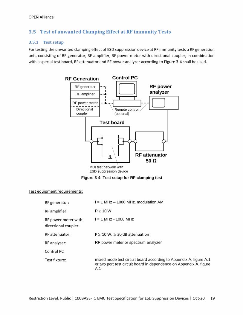
3.5 Test of unwanted Clamping Effect at RF immunity Tests
3.5.1 Test setup
For testing the unwanted clamping effect of ESD suppression device at RF immunity tests a RF generation
unit, consisting of RF generator, RF amplifier, RF power meter with directional coupler, in combination
with a special test board, RF attenuator and RF power analyzer according to Figure 3-4 shall be used.
RF Generation
Test board
RF attenuator
50 Ω
MDI test network with
ESD suppression device
Remote control
(optional)
RF generator
RF amplifier
RF power meter
Directional
coupler
RF power analyzer
Control PC
Figure 3-4: Test setup for RF clamping test
Test equipment requirements:
RF generator: f = 1 MHz – 1000 MHz, modulation AM
RF amplifier: P 10 W
RF power meter with
directional coupler:
f = 1 MHz - 1000 MHz
RF attenuator: P 10 W, 30 dB attenuation
RF analyser: RF power meter or spectrum analyzer
Control PC
Test fixture: mixed mode test circuit board according to Appendix A, figure A.1 or two port test circuit board in dependence on Appendix A, figure A.1

OPEN Alliance
Restriction Level: Public | 100BASE-T1 EMC Test Specification for ESD Suppression Devices | Oct-20 20
3.5.2 Test procedure and parameters
The required tests are defined in Table 3-7 and should be performed on one samples.
Parameter Description
Frequency: Range Step
1 MHz to 10 MHz 0.25 MHz
10 MHz to 100 MHz 1 MHz
100 MHz to 200 MHz 2 MHz
200 MHz to 400 MHz 4 MHz
400 MHz to 1000 MHz 10 MHz
Dwell time per step: 1 s
Modulation: AM 80 % 1 kHz (CWAM PP ˆˆ )
Test parameter: CMR value
Test circuit:
RF attenuator
(50 Ω)
100BASE-T1
CMC (200µH)
1 2
3 4
Test board
RF generation
(50 Ω) ESD suppression device
MDI test network
P_in P_out
Note: The used CMC should fulfil the requirements of [OPEN1].
Calculation of MDI test network CMR value: CMR(f) = P_in(f) – P_out(f)
Test power level: Controlled forward power [dBm] for classes according to Figure B-5
Evaluation of clamping
effect:
Maximum deviation of 1 dB from CMR reference value at 20 dBm for
test power level according to limit classes
Test procedure: 1. test with test power 20 dBm for setting the reference value for CMR
2. test with power level class I according to Figure B-5
3. test with power level class II according to Figure B-5
4. test with power level class III according to Figure B-5
Table 3-7: Test parameters for RF clamping test
OPEN Alliance
Restriction Level: Public | 100BASE-T1 EMC Test Specification for ESD Suppression Devices | Oct-20 21
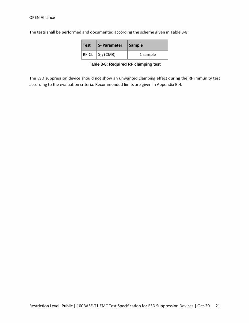
The tests shall be performed and documented according the scheme given in Table 3-8.
Test S- Parameter Sample
RF-CL S21 (CMR) 1 sample
Table 3-8: Required RF clamping test
The ESD suppression device should not show an unwanted clamping effect during the RF immunity test
according to the evaluation criteria. Recommended limits are given in Appendix B.4.

OPEN Alliance
Restriction Level: Public | 100BASE-T1 EMC Test Specification for ESD Suppression Devices | Oct-20 22
Appendix A - Test Circuit Boards
A.1 General requirements for test fixtures
A printed circuit board design with RF board-to-coax connectors shall be used for all test fixtures. To
ensure reliable RF parameters of the test fixture, a PCB with at least two layers with enlarged GND
reference plane is required. The traces on the test board should be designed as 50 (+/- 5) Ohm single
ended transmission line with a length as short as possible. For design of footprint the related specification
of ESD suppression device manufacturer have to be meet.
For S-Parameter 3-Port test fixture additional specific requirements are defined in section A.2.
In general the test fixture design and the method of connecting the ESD suppression device with the test
fixture shall allow high accuracy and reproducible test results.
A.2 Self-balance requirements for S-Parameter test fixture
The 3-Port test fixture (test circuit board with soldered RF connectors) used for balance measurement
shall have a very high grade of self-balance. To ensure the test fixture self-balance characteristic of
symmetrical network at logical port 2 (common mode), the traces between the DUT and all resistors (R1,
R2 and R3) must kept highly symmetric and as short as possible.
To prove the test fixture self-balance characteristic, the test parameter and requirements given in Table
A-1 are defined.

OPEN Alliance
Restriction Level: Public | 100BASE-T1 EMC Test Specification for ESD Suppression Devices | Oct-20 23
Parameter Description
Frequency range: 1 MHz to 1 GHz, logarithmic scale
S-Parameter: Ssd21 (DCMR), log. magnitude in dB
VNA measurement
circuit:
Port definitions:
Differential mode input (logical port 1): 50 Ω impedance each
Common mode output (logical port 2):
symmetrical single ended network with 200 Ω impedance
R = R1||R2 + R3 + RVNA port 2a
124
49.9
49.9 DUT not soldered
VNA port 1a (50 Ohm)
VNA port 1b (50 Ohm)
Logical
port 1
3-Port test fixture R1
R2
R3 Logical
port 2
Note: The DUT shall be not soldered at the fixture self-balance
measurement.
Requirement:
𝐷𝐶𝑀𝑅 ≥
(
75 1 ≤ 𝑓 ≤ 10
75 − 20𝑙𝑜𝑔 (𝑓
10) 10 ≤ 𝑓 ≤ 100
55 − 33𝑙𝑜𝑔 (𝑓
100) 100 ≤ 𝑓 ≤ 200)
𝑑𝐵, frequency f in MHz
Table A-1: Test parameters and requirements for 3-Port test fixture
10
20
30
40
50
60
70
80
90
100
1 10 100 1000
Limit
[dB]
[MHz]
S-Parameter measurement ESD supression device for 100BASE-T1Item: Self-balance requirement for 3-Port test fixture
Differential to Common mode Rejection (Ssd21)
f [MHz] DCMR [dB]
1 7510 75
100 55200 45

OPEN Alliance
Restriction Level: Public | 100BASE-T1 EMC Test Specification for ESD Suppression Devices | Oct-20 24
A.3 Example for test fixture S-Parameter measurement
The reference points by calibration are the pads of the DUT at the test fixture board.
Figure A-1: Example Test fixture S-Parameter measurement - mixed mode, top layer
Figure A-2: Example Test fixture S-Parameter measurement - single ended, top layer
OPEN Alliance
Restriction Level: Public | 100BASE-T1 EMC Test Specification for ESD Suppression Devices | Oct-20 25
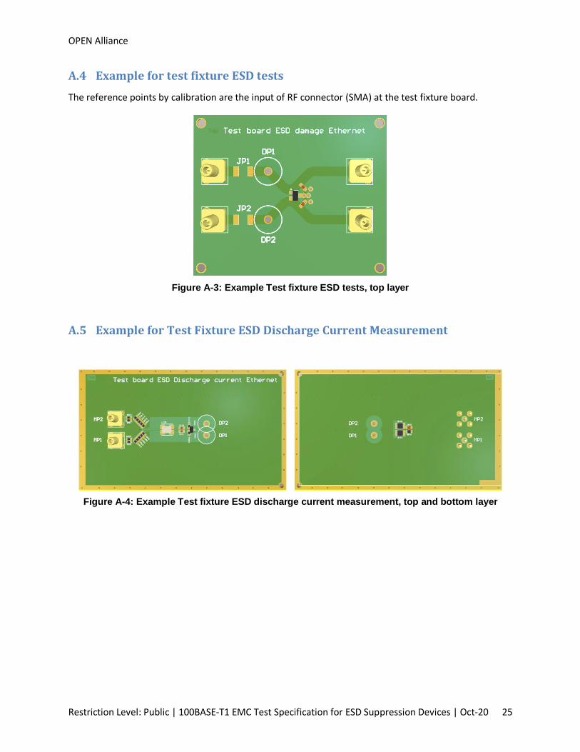
A.4 Example for test fixture ESD tests
The reference points by calibration are the input of RF connector (SMA) at the test fixture board.
Figure A-3: Example Test fixture ESD tests, top layer
A.5 Example for Test Fixture ESD Discharge Current Measurement
Figure A-4: Example Test fixture ESD discharge current measurement, top and bottom layer
OPEN Alliance
Restriction Level: Public | 100BASE-T1 EMC Test Specification for ESD Suppression Devices | Oct-20 26
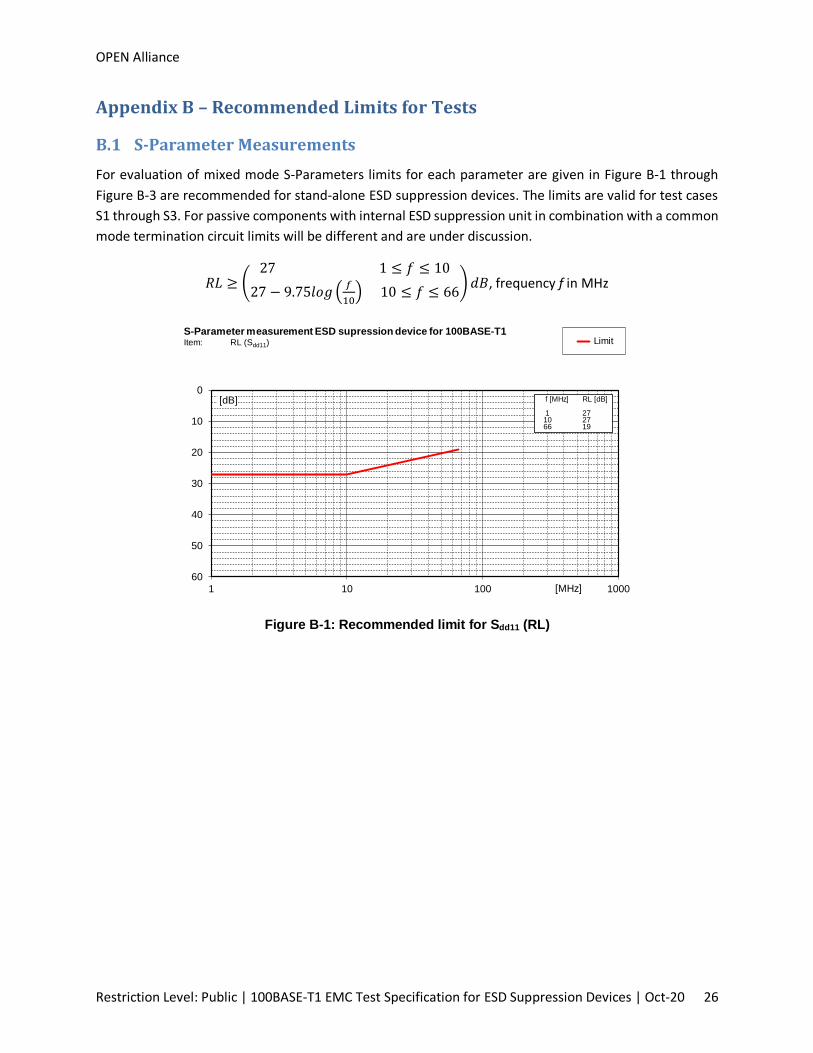
Appendix B – Recommended Limits for Tests
B.1 S-Parameter Measurements
For evaluation of mixed mode S-Parameters limits for each parameter are given in Figure B-1 through
Figure B-3 are recommended for stand-alone ESD suppression devices. The limits are valid for test cases
S1 through S3. For passive components with internal ESD suppression unit in combination with a common
mode termination circuit limits will be different and are under discussion.
𝑅𝐿 ≥ (27 1 ≤ 𝑓 ≤ 10
27 − 9.75𝑙𝑜𝑔 (𝑓
10) 10 ≤ 𝑓 ≤ 66
)𝑑𝐵, frequency f in MHz
Figure B-1: Recommended limit for Sdd11 (RL)
0
10
20
30
40
50
60
1 10 100 1000
Limit
[dB]
[MHz]
S-Parameter measurement ESD supression device for 100BASE-T1 Item: RL (Sdd11)
f [MHz] RL [dB]
1 2710 2766 19

OPEN Alliance
Restriction Level: Public | 100BASE-T1 EMC Test Specification for ESD Suppression Devices | Oct-20 27
𝐼𝐿 ≤
(
0.3 1 ≤ 𝑓 ≤ 10
0.3 + 0.2𝑙𝑜𝑔 (𝑓
10) 10 ≤ 𝑓 ≤ 33
0.4 + 0.67𝑙𝑜𝑔 (𝑓
33) 33 ≤ 𝑓 ≤ 66)
𝑑𝐵, frequency f in MHz
Figure B-2: Recommended limit for Sdd21 (IL)
𝐷𝐶𝑀𝑅 ≥
(
70 1 ≤ 𝑓 ≤ 10
70 − 20𝑙𝑜𝑔 (𝑓
10) 10 ≤ 𝑓 ≤ 100
50 − 33𝑙𝑜𝑔 (𝑓
100) 100 ≤ 𝑓 ≤ 200)
𝑑𝐵, frequency f in MHz
Figure B-3: Recommended limit for Ssd21 (DCMR)
-0,5
0,0
0,5
1,0
1,5
2,0
2,5
1 10 100 1000
Limit
[dB]
[MHz]
S-Parameter measurement ESD supression device for 100BASE-T1Item: IL (Sdd21)
f [MHz] IL [dB]
1 0.310 0.333 0.466 0.6
10
20
30
40
50
60
70
80
90
100
1 10 100 1000
Limit
[dB]
[MHz]
S-Parameter measurement ESD supression device for 100BASE-T1Item: Differential to Common mode Rejection (Ssd21)
f [MHz] DCMR[dB]
1 7010 70
100 50200 40

OPEN Alliance
Restriction Level: Public | 100BASE-T1 EMC Test Specification for ESD Suppression Devices | Oct-20 28
B.2 Damage from ESD
It is recommended that the ESD suppression device must withstand the ESD discharge with discharge
voltage amplitude of +/- 15 kV without damage.
B.3 ESD Discharge Current Measurement
For evaluation of the impact of ESD suppression device to ESD discharge current through a 100BASE-T1
transceiver simulation network limits given in Figure B-4 for positive ESD test voltages are recommended.
For negative ESD test voltages the given limits with inverted amplitudes should be applied.
Figure B-4: Recommended limits for ESD discharge current
-50
-40
-30
-20
-10
0
10
20
30
40
50
-2
0
2
4
6
8
10
12
14
16
18
40 50 60 70 80 90 100 110 120 130 140 150 160 170 180 190
Refe
ren
ce (
A)
Lim
it, R
esu
lt (
A)
Time (ns)
ESD currrent + 6kV / Example DUT
Limit Class I
Limit Class II
Limit Class III
ESD currrent + 6kV / Reference
ESD Discharge current measurement Limits for 100BASE-T1 MDI interface
t = 0 ns
Zeit [ns] Limit Class III Limit Class II Limit Class I
0 5 5 7,5
5 5 5 7,5
7 2,5 5 7,5
140 2,5 5 7,5

OPEN Alliance
Restriction Level: Public | 100BASE-T1 EMC Test Specification for ESD Suppression Devices | Oct-20 29
Table B-1 shows the relation between the required ESD robustness of the MDI interface that should be
achieved using the ESD suppression device, the ESD robustness of Ethernet transceiver to be protected,
applicable ESD test voltages and the related limit classes for the ESD suppression device.
ESD robustness requirement on MDI interface
ESD robustness of transceiver to be protected
ESD test voltages to be applied at MDI test network
Limit class for ESD suppression device
6 kV at least 2 kV and less than 6 kV 3 kV and 6 kV III
6 kV at least 4 kV and less than 6 kV 5 kV and 6 kV II
15 kV at least 2 kV and less than 15 kV 3 kV and 15 kV III
15 kV at least 4 kV and less than 15 kV 5 kV and 15 kV II
15 kV at least 6 kV and less than 15 kV 7 kV and 15 kV I
Note: The ESD robustness of transceiver to be protected is a result of ESD test according to [OPEN2].
Table B-1: Limit classes and related applied ESD test voltages

OPEN Alliance
Restriction Level: Public | 100BASE-T1 EMC Test Specification for ESD Suppression Devices | Oct-20 30
B.4 Test of unwanted Clamping Effect at RF Immunity Tests
It is recommended that the ESD suppression device doesn’t show an unwanted clamping effect during the
RF immunity test with a power level of limit class III according to Figure B-5.
Figure B-5: Test power levels for RF clamping tests at ESD suppression device
=== END OF DOCUMENT ===
10
15
20
25
30
35
40
1 10 100 1000
Pow
er
(dB
m)
Frequency (MHz)
Limit class III
Limit class II
Limit class I
[MHz] Limit class I Limit class II Limit class III
1 15 18 21
8 33 36 39
88 33 36 39
1000 27 30 33
RF clamping test