Embed Size (px)
Citation preview

V IN (V DC)
Eff
icie
nc
y (
%)
50 100 150 200 250 300 350 400 450
81.9
82.2
82.5
82.8
83.1
83.4
83.7
84
84.3
84.6
D001
TI Designs100-V/200-V AC Input 30-W Flyback Isolated Power SupplyReference Design for Servo Drives
TI Designs Design FeaturesThis reference design provides isolated 24-V DC, 16-V • 30-W Main Power Supply for Servo DrivesDC (×3), and 6-V outputs to power the control • Can Operate With DC (60-V DC to 450-V DC Max)electronics, IGBT gate drivers, communication
• Load and Line Regulation: 5%interface, and fan for 100-V and 200-V AC input servo• Peak Efficiency of 85%drives. The power supply can be either powered
directly from three-phase AC mains or can be powered • Input UV/OV, Output Overload, and SC Protectionfrom a DC link voltage. This reference design uses
• Protection Against Loss of Feedbackprimary-side regulation, quasi-resonant flyback• Lower Cost Solution Using UCC28711 Throughtopology, and is rated for a 30-W output. The line and
Primary Side Regulation, Eliminating Feedbackload regulation of the power supply is designed to beLoopwithin 5%. The power supply is designed to meet the
clearance, creepage, and isolation test voltages as per • Option of Measuring DC Link Voltage ThroughIEC61800-5 requirements. Transformer Winding
• Quasi Resonant Mode Controller Improves EMIDesign Resources• Operating Temperature Range: –10ºC to 65ºC Max
Design FolderTIDA-00315Featured ApplicationsUCC28711 Product Folder
LMS33460 Product Folder • Servo DrivesTPS54332 Product Folder • Industrial Inverters and Solar Inverters
• UPS Systems• Variable Speed AC/DC DrivesASK Our E2E Experts
WEBENCH® Calculator Tools
An IMPORTANT NOTICE at the end of this TI reference design addresses authorized use, intellectual property matters and otherimportant disclaimers and information.
1TIDUAG6A–August 2015–Revised October 2015 100-V/200-V AC Input 30-W Flyback Isolated Power Supply ReferenceDesign for Servo DrivesSubmit Documentation Feedback
Copyright © 2015, Texas Instruments Incorporated

System Description www.ti.com
1 System DescriptionAny motor drive does motor control function but beyond controlling the motor, other system functions alsoexist, such as applications management, communication, safety, HMI, and so on. Depending on the drivearchitecture, the main processor can manage multiple functions. Single-chip compact servo drives use amicrocontroller (or microprocessor) for control, application and communication. Two-chip compact servodrives use one microcontroller as well as one microprocessor to perform different functions; for example,the microcontroller manages control loop and PWM generation whereas the microprocessor managesmotion and position feedback from the motor. The power section for all servo drives contain a rectifier, DClink, inrush current limiting, and IGBT-based inverter (either discrete or using an intelligent power module[IPM]).
The main power supply, either powered directly from the AC mains or DC link is used to generate multiplevoltage rails, which are required for the operation of all the control electronics in the drive. Traditional wayof implementing the main power supply is to use fly back converter with PWM controller IC’s such as theUCC3842/UCC3843/UCC3844. Optocouplers are used for isolated feedback to regulate the outputvoltage. In case the components used in the feedback path fail, the output may reach a dangerously highlevel, damaging all the electronic components. Controllers like the UCC3842 also possess otherchallenges in limiting the power during short circuit across wide input voltage range and power dissipationin the resistors used in the startup circuit.
Most of the servo drives use IPMs for IGBT inverter stage. An IPM is a kind of modularized device,integrated by the IGBT and circuits that have the functions of signal processing, self-protection, anddiagnosis. IPMs have the advantages of small volume, light weight, simple design, and high reliability. AsIPMs have short wiring between gate drive and the IGBT, and the power levels being small, makingdriving without reverse bias possible. Many low-power IPMs operate on single 15-V (or 16-V) powersupply and use bootstrap-based gate drivers. In such a case, it is sufficient to generate a single 15 V (or16 V) with the power capability to drive all six gate drivers. Figure 1 shows an example of an IPM.
Figure 1. IPM Requiring Single 15-V Supply
2 100-V/200-V AC Input 30-W Flyback Isolated Power Supply Reference TIDUAG6A–August 2015–Revised October 2015Design for Servo Drives Submit Documentation Feedback
Copyright © 2015, Texas Instruments Incorporated

www.ti.com System Description
Figure 2 shows an IPM with an individual pre-driver. This configuration necessitates four control powersupplies: one supply for all the lower IGBTs and three individual supplies for the upper IGBTs with aproper isolation circuit. The supply voltage of each pre-driver is usually in the range of 13.5 to 16.5 V.
Figure 2. IPM Requiring Individual Power Supplies
The primary objective of this design is to design a power supply with a reduced BOM cost and a reusabledesign for drives operating at both 100-V and 200-V inputs. Other benefits include:• Constant uniform power limit throughout the input range• Reduced BOM cost using UCC28711 through primary side regulation, eliminating isolated secondary
feedback• Protection against component failure in feedback path
This reference design provides isolated 24-V DC, 16-V DC (×3), and 6-V outputs to power the controlelectronics in servo drives. The power supply can be either powered directly from three-phase AC mainsor from DC-link voltage. This reference design uses quasi resonant flyback topology and is rated for a 30-W output. The line and load regulation of the power supply is designed to be within 5%. The power supplyis designed to meet the clearance, creepage, and isolation test voltages as per IEC61800-5 requirements.
3TIDUAG6A–August 2015–Revised October 2015 100-V/200-V AC Input 30-W Flyback Isolated Power Supply ReferenceDesign for Servo DrivesSubmit Documentation Feedback
Copyright © 2015, Texas Instruments Incorporated

M
InverterDC Link
Three-phase input
90-V to 120-V AC ± 10%
200-V to 240-V AC ± 10%
Maximum DC bus voltage range
90-V to 120-V AC -> 200-V DC
200-V to 240-V AC -> 415-V DC
24 V
16 V
16 V
6 V
DC-DC
FLYBACK
CONVERTER16 V
System Description www.ti.com
Figure 3. Servo Drive Topology
1.1 Power Supply RequirementsThe main power supply requires the following to be used in servo drives applications:• Input range from 60-V DC to 450-V DC• Output power: 30 W• Switching frequency: > 40 kHz• Quasi resonant mode controller• Expected efficiency: 80%• Ripple voltage on secondaries: 500 mV• Load and line regulation: 5%• Input UV/OV shutdown• Output overload shutdown with power limit• Can be powered from AC mains or from DC link• Isolated measurement of DC-link voltage (input) through indirect technique• Detection of single-phase scenario through DC-link measurement• EMC filter and surge protection required• Ambient temperature: 65°C max• Clearance and creepage as per IEC 61800-5-2
4 100-V/200-V AC Input 30-W Flyback Isolated Power Supply Reference TIDUAG6A–August 2015–Revised October 2015Design for Servo Drives Submit Documentation Feedback
Copyright © 2015, Texas Instruments Incorporated

www.ti.com Design Features
2 Design FeaturesThis power supply design is intended for a low-cost implementation with omission of feedbackcomponents. The power supply is designed to operate across a wide input range, which suits drivesoperating from 100-V and 200-V AC inputs. The power supply includes the following protection features:• Output overvoltage fault• Input undervoltage fault• Internal over-temperature fault• Primary overcurrent fault
2.1 Topology SelectionFlyback topology is the most widely used SMPS topology in most of the variable speed drives; the powerrating is below 150 W and it requires only a single magnetic element. This criterion serves isolation andstep-up/step-down conversions as well as stores energy. Flyback topology does not require any outputinductors other topologies demand. Other advantages include easy-to-create multiple output voltages, avery low component count and is affordable.
2.2 Design RequirementsTo translate the aforementioned requirements to the sub-system level, the PWM controller, MOSFETs,and transformer require the following:• PWM controller
– Accurate voltage and constant current regulation primary-side feedback– Primary-side feedback, eliminating the need for optocoupler feedback circuits– Discontinuous conduction mode with valley switching to minimize switching losses– Protection functions including
• Input/output overvoltage fault• Input undervoltage fault• Internal overtemperature fault• Primary overcurrent fault• Loss of feedback signal
• Power MOSFETs– Should have a rated VDS ≥ 650 V to support a 450-V DC input– Should support a 1.5-A (min) drain current
5TIDUAG6A–August 2015–Revised October 2015 100-V/200-V AC Input 30-W Flyback Isolated Power Supply ReferenceDesign for Servo DrivesSubmit Documentation Feedback
Copyright © 2015, Texas Instruments Incorporated

Design Features www.ti.com
• Transformer specifications (as per IEC61800-5-1)– Four isolated secondary outputs and one isolated auxiliary winding (see Figure 4):
• Vout1 = 24 V/24 W• Vout2 = 16 V/1 W• Vout3 = 16 V/1 W• Vout4 = 16 V/1 W• Vaux = 15 V/6 W
– Switching frequency = 67 kHz– Primary to secondary isolation = 7.4 kV for 1.2/50-μs impulse voltage– Type test voltage:
• Primary to Secondary = 3.6 kVRMS
• Secondary1 to Secondary2 = 1.8 kVRMS
• Secondary2 to Secondary3 = 1.8 kVRMS
• Secondary3 to Secondary4 = 1.8 kVRMS
• Secondary1 to Secondary4 = 1.8 kVRMS
– Spacings:• Primary to Secondary clearance = 8 mm• Secondary1 to Secondary2 clearance = 5.5 mm• Secondary2 to Secondary3 clearance = 5.5 mm• Secondary3 to Secondary4 clearance = 5.5 mm• Creepage distance = 9.2 mm
– Functional isolation primary and secondary’s = 2-kV DC– DC isolation between secondary’s = 2-kV DC
Figure 4. Transformer Configuration
6 100-V/200-V AC Input 30-W Flyback Isolated Power Supply Reference TIDUAG6A–August 2015–Revised October 2015Design for Servo Drives Submit Documentation Feedback
Copyright © 2015, Texas Instruments Incorporated

PGND
HT+
PGND
PGND
PGND
VDDVAUX
21
VDD1
VS2
NTC3
GND4
CS5
DRV6
HV8
U1
UCC28711D
(+15V)
PGND
21
PGND
2 1
2 1
2 1
3.3µFC16
VDC_MEAS
GND
6
3
14
1 13
12
11
105
7
PRI
AUX
9
8
T1
EF25_CUS
HT+
VFBVFB
VFB
ISENSE
HT+
2200pFC19
91
R16
C1
A2
D2
1
32
24 V / 24 W
16 V / 1 W
16 V / 1 W
16 V / 1 W
60- to 450-V DC
www.ti.com Block Diagram
3 Block DiagramFigure 5 shows the simplified implementation diagram for the TIDA-00315. The transformer has fivesecondary windings (four isolated and one non-isolated). The power device is a 750-V MOSFET. Inprimary-side control, the output voltage is sensed on the auxiliary winding during the transfer oftransformer energy to the secondary.
Figure 5. Simplified Diagram of Solution
To represent the secondary output voltage on the auxiliary winding accurately, the discriminator inside theinput capacitor (IC) reliably blocks the leakage inductance reset and ringing, continuously samples theauxiliary voltage during the down slope after the ringing is diminished, and captures the error signal at thetime the secondary winding reaches zero current. The internal reference on VS is 4.05 V. Temperaturecompensation on the VS reference voltage of –0.8 mV/°C offsets the change in the output rectifier forwardvoltage with temperature. The feedback resistor divider is selected as outlined in the VS pin description.
7TIDUAG6A–August 2015–Revised October 2015 100-V/200-V AC Input 30-W Flyback Isolated Power Supply ReferenceDesign for Servo DrivesSubmit Documentation Feedback
Copyright © 2015, Texas Instruments Incorporated

Output Current
Outp
ut V
oltage (
V)
4.75
5.25
1
±5
2
3
4
5
tSMPL
VOCV
IOCC
tLK_RESET
tSMPL
tDM
VS Ring (p-p)
Time
Vs
Block Diagram www.ti.com
3.1 Primary-Side Current RegulationWhen the average output current reaches the regulation reference in the current control block, thecontroller operates in frequency modulation mode to control the output current at any output voltage at orbelow the voltage regulation target as long as the auxiliary winding can keep VDD above the undervoltagelockout (UVLO) turn-off threshold.
Figure 6. Aux Waveform Sampling
Figure 7. Power Limit
8 100-V/200-V AC Input 30-W Flyback Isolated Power Supply Reference TIDUAG6A–August 2015–Revised October 2015Design for Servo Drives Submit Documentation Feedback
Copyright © 2015, Texas Instruments Incorporated

www.ti.com Highlighted Products
4 Highlighted ProductsThis reference design features the following devices, which were selected based on their specifications:• UCC28711: Constant-voltage, constant-current PWM controller with primary-side regulation• LMS33460: 3-V undervoltage detector• TPS54332: 3.5 to 28-V input, 3.5-A, 1-MHz step-down converter with Eco-mode
For more information on these devices, see their respective product folders at TI.com or click on the linksunder Design Resources.
5 Component Selection and Circuit Design
5.1 Component SelectionThe following components are selected based on their specifications.
5.1.1 UCC28711The UCC28700 is a flyback power supply controller that provides accurate voltage and constant currentregulation with primary-side feedback, eliminating the need for optocoupler feedback circuits. Thecontroller operates in discontinuous conduction mode with valley switching to minimize switching losses.The modulation scheme is a combination of frequency and primary peak current modulation to providehigh conversion efficiency across the load range. The controller has a maximum switching frequency of130 kHz and it allows for a shut-down operation using NTC pin.
5.1.2 LMS33460The LMS33460 is an undervoltage detector with a 3.0-V threshold and extremely low power consumption.The LMS33460 is specifically designed to monitor power supplies accurately. This IC generates an activeoutput whenever the input voltage drops below 3.0 V. This part uses a precision on-chip voltage referenceand a comparator to measure the input voltage. Built-in hysteresis helps prevent erratic operation in thepresence of noise.
5.1.3 TPS54332The TPS54332 is a 28-V, 3.5-A non-synchronous buck converter that integrates a low RDS(on) high-sideMOSFET. To increase efficiency at light load, a pulse-skipping Eco-mode feature is automaticallyactivated. Current mode control with internal slope compensation simplifies the external compensationcalculations and reduces component count while allowing the use of ceramic output capacitors. A resistordivider programs the hysteresis of the input UVLO. An overvoltage transient protection circuit limits voltageovershoots during start-up and transient conditions. A cycle-by-cycle current limit scheme, frequency foldback and thermal shutdown protect the device and the load in the event of an overload condition.
9TIDUAG6A–August 2015–Revised October 2015 100-V/200-V AC Input 30-W Flyback Isolated Power Supply ReferenceDesign for Servo DrivesSubmit Documentation Feedback
Copyright © 2015, Texas Instruments Incorporated
C
1f
2 LC=
p
60
40Cf 67 k 10 2.1kHz
-
= ´ =
40C SW
Att
f f 10= ´
( ) ( ) ( )DCMIN ACMAX ACMAXV (V 1.414) 0.15 V 1.4141 320 1.414 0.15 320 1.414 520.352 V= ´ + ´ ´ = ´ + ´ ´ =
INMAXINRMS
ACMIN
P 37.5I 0.555 A
1.732 65 0.63 V cos= = =
´ ´´ ´ Æ
OUT
INMAX
P 30P 37.5 W
0.8= = =
h
Component Selection and Circuit Design www.ti.com
5.2 Circuit Design
5.2.1 Input SectionThe AC input is full-wave rectified by diodes D4 through D6 and D14 through D16. Fusible resistors RF1through RF3 provide in-rush current limiting and protection against catastrophic circuit failure. CapacitorC7 is used to filter the rectified AC supply. There is a provision to filter the DC input using two inductors L2and L3.
5.2.1.1 Input Diode BridgeThe input bridge is selected by using the following equations:
(1)
(2)
where• cosø is the power factor, which is assumed to be 0.6
The minimum voltage rating of the rectifier is given by Equation 3:
(3)
Considering a raise in DC bus voltage due to regenerative action, diodes with 1000-V, 1-A ratings areused for the three-phase bridge rectifier.
5.2.1.2 Input Capacitors (CIN)The DC input bulk capacitor C7 provides a smooth DC voltage by filtering low frequency AC ripple voltage.
A single 22-μF/500-V capacitor (UCY2H220MHD) is connected as DC bulk capacitor. Based on therequirement on input side, this capacitor value can be changed.
5.2.1.3 Input Filter InductorsThe required corner frequency of the filter is given by Equation 4:
(4)
where• fC is the desired corner frequency of the filter• fSW is the operating frequency of the power supply (67 kHz)
Assuming a 60-dB attenuation at the switching frequency of the power supply, the cut-off frequency of thefilter is given by
(5)
The cut-off frequency can also be calculated using Equation 6:
(6)
Back-calculating the value of inductor required using Equation 6 leads to an inductance of 60 μH, whichcan be split into two to be placed on both the lines of the DC bus.
NOTE: For this design, none of the inductors are used. L1 and L2 are just replaced by a short.
10 100-V/200-V AC Input 30-W Flyback Isolated Power Supply Reference TIDUAG6A–August 2015–Revised October 2015Design for Servo Drives Submit Documentation Feedback
Copyright © 2015, Texas Instruments Incorporated

PGND
VDD
VDD1
VS2
NTC3
GND4
CS5
DRV6
HV8
U1
UCC28711D
10 µFC16
HT+
( ) ( )
VDD(ON)
HV START CDDSVDD
I I dt 250 1.5 1C 11.83 F
21V
- ´ m - m ´= = = m
1
2
3
J1
1714968
DC+
1
2
3
J4
1714984
PE
PE
60 - 450Vdc
DC Input
3PhaseAC Input (40-320Vac)
1000V
D41N4007
1000V
D51N4007
1000V
D61N4007
1000V
D1
1N4007
1000V
D141N4007
1000V
D151N4007
1000V
D161N4007
PGND
1.0
RF1
1.0
RF2
1.0
RF3
RV1 RV2
RV3
2200pF
C10
2200pF
C11
2200pF
C12
0.1µFC9 22uF
C7UCY2H220MHD
L2
768772102
L3
768772102
DC-
DC-
VBUS
www.ti.com Component Selection and Circuit Design
Figure 8. Input Section
5.2.1.4 Surge ProtectionConsidering 320-V AC input with a 10% variation, MOV of 390-V AC with a peak current rating of 2500 Aspecified for 8/20-μs waveform has been used to suppress surge at the input. For 100-V rated drives, thevoltage rating of the MOV needs to be lowered.
5.2.2 Controller Section
5.2.2.1 VDD Capacitor Selection (CDD)The capacitance on VDD needs to supply the device operating current until the output of the converterreaches the target minimum operating voltage in constant-current regulation. At this time the auxiliarywinding can sustain the voltage to the UCC28711 family. The total output current available to the load andto charge the output capacitors is the constant-current regulation target. The CVDD is selected usingEquation 7 based on the desired startup time (dtCDDS) of the UCC28700 controller and knowing the startcurrent (ISTART), as well as, the UCC28711 device startup threshold (VVDD(on)). Assuming startup time for thedevice (dtCDDS) is 1 second, the value of VDD capacitor can be calculated as in Equation 7. The startcurrent for the UCC28711 is 1.5 μA, the start-up threshold VVDD(on) is 21 V, and IHV is 250 μA (typ).
(7)
In this design, a 10-μF capacitor is used on VDD pin.
Figure 9. VDD Capacitor
11TIDUAG6A–August 2015–Revised October 2015 100-V/200-V AC Input 30-W Flyback Isolated Power Supply ReferenceDesign for Servo DrivesSubmit Documentation Feedback
Copyright © 2015, Texas Instruments Incorporated

OUT
PM 2 2
PPK MAX
2 P 2 30 W
0.8L 154.7 H
I f 2.69 67 kHz
´ ´
= = = m
´
h
´
OUTPPK
INMIN MAX
2 P 2 30I 2.475 A
V D 0.8 60 0.505
´ ´= = =
h´ ´ ´ ´
RMAX MAG MAXD 1 D f 1 0.425 70 k 0.505
2 2
T 2= - - = - - =
m
V = 21 VVDD(ON)
VVDD
V = 8 VVDD(OFF)
0 V
DRV
3 Initial DRV Pulses After VDD(ON)
Component Selection and Circuit Design www.ti.com
Note that after CVDD has been charged up to the device turn-on threshold (VVDD(on)), the UCC28711 initiatesthree small gate drive pulses (DRV) and start sensing current and voltage (see Figure 10). If a fault isdetected, such as an input undervoltage, the UCC28711 terminates the gate drive pulses and dischargesCDD to initiate an undervoltage lockout. This capacitor will be discharged with the run current of theUCC28711 (IRUN) until the VDD turnoff (VVDD(off)) threshold is reached. Note the CDD discharge time (tCDD)from this forced soft start can be calculated knowing the controller run current (IRUN) without out gatedriver switching, the controller’s VDD turnoff threshold (VVDD(off)), and the following equations. If no fault isdetected, the UCC28711 continues to drive the MOSFET and control the input and output currents, and asoft start will not be initiated.
Figure 10. Power-On Sequence
5.2.2.2 Calculation of Duty CycleThe transformer demagnetizing duty cycle (DMAG) is fixed to 42.5% based on the UCC28711 control lawmethodology.DMAG = 0.425
TR is the estimated period of the LC resonant frequency at the switch node.TR = 2 µs
Calculate maximum duty cycle (DMAX):
(8)
5.2.2.3 Calculation of Transformer Peak CurrentCalculate the transformer primary peak current (IPPK) based on a minimum flyback input voltage. Thiscalculation includes the reduction in flyback input voltage caused by the ripple voltage across the inputcapacitor.
(9)
5.2.2.4 Transformer Calculations
5.2.2.4.1 Calculation of Primary Inductance (LPM)The primary magnetizing inductance (LPM) is selected based on minimum flyback input voltage,transformer, primary peak current, efficiency, and maximum switching frequency (fMAX).
(10)
The design uses a transformer with LPM equal to 150 μH.
12 100-V/200-V AC Input 30-W Flyback Isolated Power Supply Reference TIDUAG6A–August 2015–Revised October 2015Design for Servo Drives Submit Documentation Feedback
Copyright © 2015, Texas Instruments Incorporated

( ) ( )OUTAUX _PK RMS
OUT MAG
P 2 12I 15 V Output 1.788 A 0.672 A
V D 15.8 0.425
´= = =
´ ´
( ) ( )OUTS4PK RMS
OUT MAG
P 2 2I 16 V Output 0.28 A 0.105 A
V D 16.8 0.425
´= = =
´ ´
( ) ( )OUTS3PK RMS
OUT MAG
P 2 2I 16 V Output 0.28 A 0.105 A
V D 16.8 0.425
´= = =
´ ´
( ) ( )OUTS2PK RMS
OUT MAG
P 2 2I 16 V Output 0.28 A 0.105 A
V D 16.8 0.425
´= = =
´ ´
( ) ( )OUTS1PK RMS
OUT MAG
P 2 48I 4.55 A 1.714 A
V D 24.824 V O
0.4utp t
2u
5
´= = =
´ ´
SRMS SMAG
PK
DI I
3=
PRMS PPKMAX 0.505
I I 2.475 1.0151 A3 3
D= = ´ =
DDMIN DEAS
OUT _INIT DG
A
S
V V 8 0.8N 0.64
V V 13.
N
8N
+ += = = =
+
( )( )
MAX INMIN QAON RCS
PS
MAG O
P
UT
PM
GS SM D
D V 2 0N L
N L
.6 V V
N 2.5D V V
´ ´ - -= = = »
´ +
www.ti.com Component Selection and Circuit Design
5.2.2.4.2 Calculation of Turns RatioAssuming:• VQAON = 2 V, estimated voltage drop across FET during conduction• VRCS = 0.75 V, voltage drop across current sense resistor• VDG = 0.8 V, estimated forward voltage drop across output diode
The transformer turns ratio primary to secondary (NPS) is calculated in Equation 11 based on volt-secondbalance. Note in the Equation 11, LSM is the secondary magnetizing inductance.
(11)
Assuming:• VDDMIN = 8 V, UCC28711 minimum VDD voltage before UVLO turnoff• VDE = 0.8 V, estimated auxiliary diode forward voltage drop• VOUT_INIT = 13 V, minimum voltage on the output at initial turn on.
The transformer auxiliary to secondary turns ratio (NAS) is calculated in Equation 12.
(12)
5.2.2.4.3 Calculation of Transformer Primary RMS Current (IPRMS)
(13)
5.2.2.4.4 Calculation of Transformer Secondary RMS Current (ISRMS)Transformer secondary peak currents (ISPK) are calculated and RMS currents for each secondary arecalculated using the following equations:
(14)
(15)
(16)
(17)
(18)
(19)
13TIDUAG6A–August 2015–Revised October 2015 100-V/200-V AC Input 30-W Flyback Isolated Power Supply ReferenceDesign for Servo DrivesSubmit Documentation Feedback
Copyright © 2015, Texas Instruments Incorporated

PGND
PGND
VDD
VDD1
VS2
NTC3
GND4
CS5
DRV6
HV8
U1
UCC28711D
PGND
600V
D241N4937-E3
3300pF
C17
3.3µFC16
30.1kR18
205R9
86.6kR11
VFB
( ) ( )S1 VSR
S2AS OCV F VSR
R V 86.8K 4.05R 30.061kΩ (Rounded off to 28 k )
N V V V 0.64 24.6 4.05
´ ´= = = W
´ + - ´ -
AS AS
PS PS
VSL(RUN) VSL
INMIN I
(
NMIN
SU
1R N)
0.64V 2 0.8 V 0.8 100 0.82.5R 91k (Rounded off to 86.8 k )
22
N N
N N
I I 5
´ ´ ´
= = = = W Wm
Component Selection and Circuit Design www.ti.com
5.2.2.5 Primary Side RegulationIn primary-side control, the output voltage is sensed on the auxiliary winding during the transfer oftransformer energy to the secondary. To represent the secondary output voltage on the auxiliary windingaccurately, the discriminator (inside the UCC28711) reliably blocks the leakage inductance reset andringing, continuously samples the auxiliary voltage during the down slope after the ringing is diminished,and captures the error signal at the time the secondary winding reaches zero current. The internalreference on VS is 4.05 V; it is connected to a resistor divider from the auxiliary winding to ground. Theoutput-voltage feedback information is sampled at the end of the transformer secondary currentdemagnetization time to provide an accurate representation of the output voltage. Timing information toachieve valley-switching and to control the duty cycle of the secondary transformer current is determinedby the waveform on the VS pin. Do not place a filter capacitor on this input, which would interfere withaccurate sensing of this waveform.
The VS pin also senses the bulk capacitor voltage to provide for AC input run, stop thresholds, andcompensate the current-sense threshold across the AC input range. This information is sensed during theMOSFET on-time. For the AC-input run/stop function, the run threshold on VS is 225 μA and the stopthreshold is 80 μA. A wide separation of run and stop thresholds allows clean start-up and shut-down ofthe power supply with the line voltage.
The values for the auxiliary voltage divider upper-resistor RS1 and lower-resistor RS2 can be determinedby the following equations. Note RS1 so the converter will go into UVLO when the input is below 80% ofthe minimum specified input voltage.
(20)
where• NAS and NPS: transformer turns ratios• IVSL(run): the run-threshold for the current pulled out of the VS pin during the MOSFET on-time (equal to
220 µA max from the UCC28711 datasheet)
(21)
where• VOCV: regulated output voltage of the converter• VF: secondary rectifier forward voltage drop at near-zero current• NAS: transformer auxiliary-to-secondary turns ratio• RS1: the VS divider high-side resistance• VVSR: CV regulating level at the VS input (equal to 4.05 V typical from the UCC28711 datasheet)
Figure 11. Primary Feedback
14 100-V/200-V AC Input 30-W Flyback Isolated Power Supply Reference TIDUAG6A–August 2015–Revised October 2015Design for Servo Drives Submit Documentation Feedback
Copyright © 2015, Texas Instruments Incorporated

2 2OSSCOSS FLY MAX
C 23 pP V f 432.57 67 k 0.144 W
2 2= ´ ´ = ´ ´ =
( )( ) ( )( )PPK r MAX
SW FLY OUT VDG PS
I t f 2.69 52.5 n 67 kP V V V N 432.57 24 0.8 2.5 1.75 W
2 2
´ ´ ´ ´= - + ´ = - + ´ =
FLY INMAX FDINRIPPL
AE 36.76
V V 2 2 V 320 2 2 0.8 432.572
V
2= ´ - - ´ = ´ - - ´ = V
0
3
6
9
12
15
0 3 6 9 12 15
Qg (nC)
VG
S(V
)
VDS = 480 V
ID = 3.5 A
gDS r
drive
Q 2 9.2 nC 2Estimated V rise and fall time t 92 ns
I 0.2 A
´ ´
= = = =
www.ti.com Component Selection and Circuit Design
The output overvoltage function is determined by the voltage feedback on the VS pin. If the voltagesample on VS exceeds 115% of the nominal VOUT, the device stops switching and the internal currentconsumption is IFAULT, which discharges the VDD capacitor to the UVLO turn-off threshold. After that, thedevice returns to the start state and a start-up sequence ensues.
Protection is included in the event of component failures on the VS pin. If a complete loss of feedbackinformation on the VS pin occurs, the controller stops switching and restarts.
5.2.2.6 MOSFET SelectionTo meet the required voltage and current specifications, 650-V/7-A rated MOSFET (AOT7S65) with thefollowing characteristics has been chosen:• RDS(on) = 0.65 Ω• COSS = 23 pF
The maximum FET gate drive turn ON current (limited by the UCC28711) is IDRIVE = 0.025 A (maximumgate sink current is internally limited and is approximately 0.2 A).
Qg = 9.2 nC, gate charge just above the miller plateau.
(22)
Power loss by driving the FET’s gate (Pg):
• Pg = 14 V × Qg × fMAX = 14 V × 13 nC × 67k = 12.2 mW• Qg1, Gate charge at 14 V drive (see Figure 12)• Vg = 14 V (from UCC28711 datasheet)
Figure 12. Gate-Charge Characteristics for MOSFET
Calculating the average input voltage to the flyback at the maximum input voltage (VINMAX):
(23)
FET average switching loss (PSW):
(24)
FET COSS power dissipation (PCOSS):
Average FET drain to source capacitance = 23 pF
(25)
15TIDUAG6A–August 2015–Revised October 2015 100-V/200-V AC Input 30-W Flyback Isolated Power Supply ReferenceDesign for Servo DrivesSubmit Documentation Feedback
Copyright © 2015, Texas Instruments Incorporated

LC S1 CS D PALC
P
K R R T N 25 86.8 K 0.27 300 n 2.5 R 2.93 k
L 150 µ
´ ´ ´ ´ ´ ´ ´ ´= = = W
2 2
RCS PRMS CSP I R 1.1 0.27 0.3267 W= ´ = ´ =
CS
PPK
0.75 0.75R 0.278
I 2.69= = = W
2 2
RDSON PRMS DSONP I R 1 .1 0.65 0.786 W= ´ = ´ =
Component Selection and Circuit Design www.ti.com
Power loss from RDS(on) (PRDSON)
(26)
Total power loss per MOSFET = 1.75 + 0.0122 + 0.786 + 0.144 = 2.6922 W
5.2.2.7 MOSFET Thermal CalculationsThermal resistance of MOSFET, junction to case, max = 1.2°C/W
Thermal resistance of heat sink, max = 9°C/W (for heat sink 513201B02500G)
MOSFET temperature rise = (1.2 + 9) × 2.7362 = 28°
With an ambient temperature varying from −20°C/W to 65°C/W, the FET temperature would be in therange from 8°C to 93°C (less than 150°C as specified in datasheet).
A MOSFET with voltage rating of ≥650 V can be used if a higher de-rating is required to enhancereliability.
5.2.2.8 Current SensingBased on a nominal maximum current sense signal of 0.75 V, the sense resistor is calculated as given inEquation 27.
(27)
The actual value of sense resistor needs to be tuned based on the allowable power limit during faultconditions. In this design, a 0.27-Ω resistor is used as RCS.
Nominal current sense resistor power dissipation is calculated in Equation 28.
(28)
The UCC28711 always operates with cycle-by-cycle primary peak current control. The normal operatingrange of the CS pin is 0.78 to 0.195 V. There is additional protection if the CS pin reaches 1.5 V, whichresults in a UVLO reset and restarts sequence.
5.2.2.9 Line CompensationThe current-sense (CS) pin is connected through a series resistor (RLC) to the current-sense resistor (RCS).The current-sense threshold is 0.75 V for IPP(max) and 0.25 V for IPP(min). The series resistor RLC providesthe function of feed-forward line compensation to eliminate change in IPP due to change in di/dt and thepropagation delay of the internal comparator and MOSFET turn-off time. There is an internal leading-edgeblanking time of 235 ns to eliminate sensitivity to the MOSFET turn-on current spike. The value of RCS isdetermined by the target output current in constant-current (CC) regulation. The value of RLC can bedetermined by Equation 29:
(29)
where• RLC: Line compensation resistor• RS1: VS pin high-side resistor value• RCS: current-sense resistor value• TD: current-sense delay including MOSFET turn-off delay; add 50 ns to MOSFET delay• NPA: transformer primary-to-auxiliary turns ratio• LP: transformer primary inductance• KLC: current-scaling constant (equal to 25 A/A from datasheet of UCC28711)
16 100-V/200-V AC Input 30-W Flyback Isolated Power Supply Reference TIDUAG6A–August 2015–Revised October 2015Design for Servo Drives Submit Documentation Feedback
Copyright © 2015, Texas Instruments Incorporated

PGND
VDD1
VS2
NTC3
GND4
CS5
DRV6
HV8
U1
UCC28711D
ISENSE
HT+
0.27
R19
1
32
Q1
AOT7S65
1
23
Q4
2N7002P,215
PGND
GATE
HS1
513201B02500G
PGND
VDD1
VS2
NTC3
GND4
CS5
DRV6
HV8
U1
UCC28711D
ISENSE
ISENSE
HT+
2200pFC19
91
R16
0.27R19
1
32
Q1AOT7S65
1
23
Q42N7002P,215
PGND
GATE
www.ti.com Component Selection and Circuit Design
NOTE: The value of RLC may require adjustments based on the noise or ringing on the current sensewhich is dependent on routing of the signals. A 91-Ω resistor is used in the design.
Figure 13. Current Sense
5.2.2.10 MOSFET Gate-DriveThe DRV pin of the UCC28711 is connected to the MOSFET gate pin, usually through a series resistor.The gate driver provides a gate-drive signal limited to 14 V. The turn-on characteristic of the driver is a 25-mA current source, which limits the turn-on dv/dt of the MOSFET drain and reduces the leading-edgecurrent spike, but still provides gate-drive current to overcome the Miller plateau. The gate-drive turn-offcurrent is determined by the low-side driver RDS(on) and any external gate-drive resistance. To improve theefficiency and reduce switching loss in the power device, an external BJT based current buffer may beused to drive MOSFET’s with higher voltage rating having high Qg.
Figure 14. MOSFET Gate Drive
The turning off the MOSFET Q1 (in case of undervoltage and overvoltage condition) is taken care by theLMS33460 (as explained in Section 5.2.4.1). However, the output of the LMS33460 is also connected tothe gate of MOSFET Q1 through another smaller switch Q4. This will take care of any kind of turn-off ofthe device (the three pulses that comes from the device while starting the switching are also prevented).
17TIDUAG6A–August 2015–Revised October 2015 100-V/200-V AC Input 30-W Flyback Isolated Power Supply ReferenceDesign for Servo DrivesSubmit Documentation Feedback
Copyright © 2015, Texas Instruments Incorporated

OUT _ AUX FDG _ AUXDG _ AUX
OUT _ AUX
P V 6 0.875P 0.35 W
V 15
´ ´
= = =
INMAXRDG _ AUX OUT_AUX
PS
V 2 320 2V V 1 5 137 V
3.N 7= + = + =
OUT2 FDG2DG2
OUT2
P V 1 0.875P 0.054 W
V 16
´ ´
= = =
DG2PK AUX _PK
0.28 AI I
0.105 Arms= =
INMAXRDG2 OUT2
PSN
V 2 320 2V V 1 6 138 V
3.7= + = + =
OUT1 FDGDG1
OUT
P V 24 1.25P 1.25 W
V 24
´ ´
= = =
DG1PK S1PKI I 4.55 A= =
INMAX
RDG1 OUT1
PSN
V 2 320 2V V 24 205 V
2.5= + = + =
Component Selection and Circuit Design www.ti.com
5.2.3 Output Diodes
5.2.3.1 24-V Output DiodeCalculate diode reverse voltage (VRDG)
(30)
Calculate peak output diode (IDGPK)(31)
This design uses a schottky diode with a 4-A/400-V rating (MUR440) with a forward voltage drop (VFDG) of1.25 V. VFDG = 1.25 V; Estimated diode power loss (PDG).
(32)
5.2.3.2 16-V Auxiliary Output DiodeCalculate diode reverse voltage (VRDG)
(33)
Calculate peak output diode (IDG2PK)
(34)
This design has a 3-A, 200-V super-fast rectifier (MURS320-13-F) with a forward voltage drop (VFDG) of875 mV at 3 A.
Estimated diode power loss (PDG2)
(35)
NOTE: The same diode has been used for all 16-V outputs.
5.2.3.3 15-V Auxiliary Output DiodeCalculate diode reverse voltage (VRDG)
(36)
Calculate peak output diode (IDG2PK)IAUX_PK = 1.788 A (0.672 ARMS)
This design uses a 3-A, 200-V Super-fast rectifier (MURS320-13-F) with a forward voltage drop (VFDG) of875 mV at 3 A.
Estimated diode power loss (PDG_AUX)
(37)
18 100-V/200-V AC Input 30-W Flyback Isolated Power Supply Reference TIDUAG6A–August 2015–Revised October 2015Design for Servo Drives Submit Documentation Feedback
Copyright © 2015, Texas Instruments Incorporated

2 2
COUT _RMS _ AUX
1.788 0.425 6I 0.716 A
153
æ ö´ æ ö= - =ç ÷ ç ÷ç ÷ è øè ø
2 2
COUT _RMS _16V
0.28 0.425 1I 85 mA
163
æ ö´ æ ö= - =ç ÷ ç ÷ç ÷ è øè ø
MAG OU
2 22 2SPK
COUT _RMS _ 2 VOUT
4T
D P
V
I 4.55 0.425 24I 1.39 A
243 3
æ ö æ ö´ æ ö ´ æ öç ÷= - = - =ç ÷ç ÷ ç ÷ç ÷ç ÷ è øè ø è øè ø
OUT _ AUX
620
15 2 C 160 µF0.025
m ´´³ =
OUT _16V
120
16 2 C 25 µF0.025
m ´´³ =
OUT
OUTOUT _ 24V
RIPPLE
P 2420 20 V 2 24 2 C 400 µF
V 0.025
m ´ m ´´ ´³ = »
RIPPLECOUT _ 24V
SPK
V 0.9 25 m 0.9ESR 4.95 m
I 4.55 A
´ ´= = » W
www.ti.com Component Selection and Circuit Design
5.2.4 Output CapacitorsSelect an output ESR based on 90% of the allowable output ripple voltage:
(38)
The output capacitor (COUT) was selected to have a ripple of less than 25 mV on VOUT.
(39)
Two numbers of 330-μF/35-V aluminum electrolytic capacitor with a ripple current rating of 1000 mA areconnected in parallel at the output diode to support the ripple current.
(40)
A 100-μF/35-V capacitor with a ripple current ratings of 460 mA are connected at each of the 16-Voutputs.
(41)
This design uses a 220-μF/35-V capacitor with a ripple current rating of 490 mA.
Estimate the total output capacitor RMS current (ICOUT_RMS)
(42)
(43)
(44)
19TIDUAG6A–August 2015–Revised October 2015 100-V/200-V AC Input 30-W Flyback Isolated Power Supply ReferenceDesign for Servo DrivesSubmit Documentation Feedback
Copyright © 2015, Texas Instruments Incorporated

VDD1
VS2
NTC3
GND4
CS5
DRV6
HV8
U1
UCC28711D
2.00MegR7
2.00MegR10
2.00MegR13
GND3
VIN5
NC1
GND*2
VOUT4
U2
LMS33460MG/NOPB
1
23
Q22N7002P,215
PGNDPGND
PGNDPGND
PGND
VBUSVBUS
100pFC18
511k
R14
44.2kR15
36.5kR17
7.5V
D28
GATE
Component Selection and Circuit Design www.ti.com
5.2.4.1 Overvoltage DetectionThe LMS33460 is a micro-power under voltage sensing circuit with an open drain output configuration,which requires a pull resistor. The LMS33460 features a voltage reference, a comparator with precisethresholds, and built-in hysteresis to prevent erratic reset operation. This IC generates an active outputwhenever the input voltage drops below 3.0 V. The resistor divider in Figure 15 is derived with 450-V DCas an overvoltage trip point. A Zener diode (D28) clamps the input voltage at the LMS33460 to less than 8V (absolute max of the device) when the DC bus voltage is at its max of 450-V DC.
The device has a minimum hysteresis voltage of 100 mV, which translates to approximately 11 V on theDC bus. Hysteresis can also be adjusted with R14.
Figure 15. Undervoltage Protection
The UCC28711 has NTC input, which can be used to interface an external negative temperaturecoefficient resistor for remote temperature sensing to allow user-programmable external thermalshutdown. The shutdown threshold is 0.95 V with an internal 105-μA current source, which results in a9.05-kΩ thermistor shutdown threshold. Pulling this pin low shuts down PWM action. The signal from theLMS33460 is interfaced to this pin to shut down the controller during overvoltage.
20 100-V/200-V AC Input 30-W Flyback Isolated Power Supply Reference TIDUAG6A–August 2015–Revised October 2015Design for Servo Drives Submit Documentation Feedback
Copyright © 2015, Texas Instruments Incorporated
1
2
3
J1
1714968
DC+
1
2
3
J4
1714984
PE
PE
60 - 450Vdc
DC Input
3PhaseAC Input (40-320Vac)
1000V
D41N4007
1000V
D51N4007
1000V
D61N4007
1000V
D1
1N4007
1000V
D141N4007
1000V
D151N4007
1000V
D161N4007
PGND
PGND
VDDVAUX
21
D22
MURS320-13-F
VDD1
VS2
NTC3
GND4
CS5
DRV6
HV8
U1
UCC28711D
(+15V)
HS1513201B02500G
PGND
21
D23
1SS355TE-17
3.3µFC16
600V
D91N4937-E3
1.0
RF1
1.0
RF2
1.0
RF3
RV1 RV2
RV3
2200pF
C10
2200pF
C11
2200pF
C12
0.1µFC9
100kR1
4700pFC2
HT+
22uF
C7UCY2H220MHD
Green
12
D25
L2
768772102
L3
768772102
PGND
DC-
VFB
HT+
220µFC15
DC-
VBUS
10kR8
C1
A2
D2
13
2Q1AOT7S65
1
3
Q42N7002P,215
GATE
www.ti.com Component Selection and Circuit Design
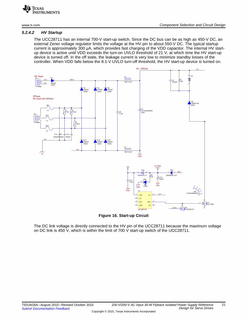
5.2.4.2 HV StartupThe UCC28711 has an internal 700-V start-up switch. Since the DC bus can be as high as 450-V DC, anexternal Zener voltage regulator limits the voltage at the HV pin to about 550-V DC. The typical startupcurrent is approximately 300 μA, which provides fast charging of the VDD capacitor. The internal HV start-up device is active until VDD exceeds the turn-on UVLO threshold of 21 V, at which time the HV start-updevice is turned off. In the off state, the leakage current is very low to minimize standby losses of thecontroller. When VDD falls below the 8.1-V UVLO turn-off threshold, the HV start-up device is turned on.
Figure 16. Start-up Circuit
The DC link voltage is directly connected to the HV pin of the UCC28711 because the maximum voltageon DC link is 450 V, which is within the limit of 700 V start-up switch of the UCC28711.
21TIDUAG6A–August 2015–Revised October 2015 100-V/200-V AC Input 30-W Flyback Isolated Power Supply ReferenceDesign for Servo DrivesSubmit Documentation Feedback
Copyright © 2015, Texas Instruments Incorporated

PGND
330UF35V
C3330UF35V
C4
600V
D8
1N4937-E3
0.1µF
C533.2R2
1.78M
R3
+24VDC
GND
VDC_MEAS
24V / 1A
6
3
14
1 13
12
11
105
7
PRI
AUX
9
8
T1
750342851
400V
D7
MUR440
+6V
+24VDC
VFB
27V
D3
L1
7447462047
1
2
3
J2 1725669
1
2
J81725656
0.1µFC6
DC _MEAS(min)
65V 16
3.75= =
DC _MEAS(max)
450V 120 V
3.75= =
Component Selection and Circuit Design www.ti.com
5.2.5 Input Voltage SensingAC input voltage and DC link voltage are measured in the drives for various reasons:1. To detect single phase failure2. DC Link undervoltage and overvoltage condition3. To control the inverter output voltage
When a drive application does not mandate high accuracy measurements, the flyback converter itself canmeasure the AC input as well as DC link voltage. When the primary switch is ON, the induced voltage atthe secondary (D8 in Figure 17) will be the DC link voltage times the turn ratio, which will also beproportional to the AC mains input voltage. This voltage is rectified and filtered with RC network. Voltagescaling can be performed based on the ADC input voltage range.
At 450-V DC input with a turns ratio of 3.75, the forward induced voltage is given by
(45)
(46)
This voltage is stepped down through a resistive divider 0.01587 to scale it to 1.9044 V and 0.25 V. Thisstep-down ratio can be adjusted based on the application requirements.
Figure 17. DC Link Voltage Measurement
22 100-V/200-V AC Input 30-W Flyback Isolated Power Supply Reference TIDUAG6A–August 2015–Revised October 2015Design for Servo Drives Submit Documentation Feedback
Copyright © 2015, Texas Instruments Incorporated

www.ti.com Component Selection and Circuit Design
5.2.6 Transformer Construction
Table 1. Magnetic Details
CORE TYPE BOBBINEE25 14-pin (vertical)
Table 2. Electrical Details of the Transformer
PARAMETER TEST CONDITIONS VALUEInductance 50 kHz, 100 mV, LS 150.0 µH ±10%
Saturation current 20% rolloff fromn initial 2.78 Atie (6+7+8+9+10+11+12+13+14), 100Leakage inductance 5 µH maxkHz, 100 mV, LS
Dielectric 1250-V AC, 1 secondTie (5+6, 9+10+11+12+13+14), 3125-VDielectric AC, 1 second
Dielectric 2500-V AC, 1 secondDielectric 2500-V AC, 1 secondDielectric 2500-V AC, 1 second
Turns ratio (5-3):(6-7) 3.75:1, ±2%Turns ratio (5-3):(8-9) 3.75:1, ±2%Turns ratio (5-3):(10-11) 3.75:1, ±2%Turns ratio (5-3):(12-13) 3.75:1, ±2%Turns ratio (5-3):(14-1) 2.5:1, ±2%
Figure 18. Transformer Pin Out
23TIDUAG6A–August 2015–Revised October 2015 100-V/200-V AC Input 30-W Flyback Isolated Power Supply ReferenceDesign for Servo DrivesSubmit Documentation Feedback
Copyright © 2015, Texas Instruments Incorporated

OUT REF
R20V V 1
R22
æ ö= ´ +ç ÷
è ø
BOOT1
VIN2
PH8
GND7
VSENSE5
COMP6
EN3
SS4
PAD9
U3
TPS54332DDAR
D29B340A-13-F
GND
GND
1500pFC25
+6V
6V / 2A
47pFC24
+24VDC
0.1µF
C20
10.2kR20
22.1kR21
1.58kR22
8200pFC23
4.7µFC26
4.7µFC21
10µFC27
10µFC22
L4
7447471100
Component Selection and Circuit Design www.ti.com
5.2.7 24-V to 6-V Switcher
Figure 19. 24-V to 6-V Switcher
A DC/DC converter TPS54332 converts 24-V DC to 6-V DC at 2 A. Note that when a 12-W output isavailable at the 6-V rail, the corresponding output power should be derated from the 24-W output.
The TPS54332 can accept input voltage from 3-V to 28-V DC on VIN pin. In this case, 24-V is directlyconnected to the VIN pin and two 4.7-μF capacitors (C26 and C21) are connected on VIN pin. The devicecan be enabled and disabled by using the EN pin. Capacitor C23 is used to decide the output rise time.With a value of 8200 pF, the slow start time is 3.28 ms.
The switching frequency of the TPS54332 is fixed at 1 MHz.
With an internal reference voltage VREF = 0.8 V, the output of the TPS54332 is set using Equation 47.
(47)
The selected values are R20 = 10.2 kΩ and R22 = 1.58 kΩ
The TPS54332 is designed to operate using an external catch diode between PH and GND. The selecteddiode must meet the absolute maximum ratings for the application. The reverse voltage must be higherthan the maximum voltage at the PH pin, which is Vin(max) + 0.5 V. The peak current must be greaterthan IOUTMAX plus half the peak-to-peak inductor current. This design uses the Diodes, Inc. B340A witha reverse voltage of 40 V, a forward current of 3 A, and a forward voltage drop of 0.5 V.
Two components need to be selected for the output filter: the output inductor L4 and the output capacitors(C22 and C27). This design uses an inductor 7447471100 (from Würth Electronics) and two capacitors ofvalue 10 μF are used in parallel. The compensation is external so loop stability can be decided as per therequirement.
24 100-V/200-V AC Input 30-W Flyback Isolated Power Supply Reference TIDUAG6A–August 2015–Revised October 2015Design for Servo Drives Submit Documentation Feedback
Copyright © 2015, Texas Instruments Incorporated

www.ti.com Test Results
6 Test Results
6.1 Functional Test Results
Figure 20. FET Voltage at 60-V Input / 30-W Output Figure 21. FET Voltage at 60-V Input / No Load Output(CH1: VDS and CH2: VGS) (CH1: VDS and CH2: VGS)
Figure 22. FET Voltage at 450-V Input / 30-W Output Figure 23. FET Voltage at 450-V Input / No Load Output(CH1: VDS and CH2: VGS) (CH1: VDS and CH2: VGS)
25TIDUAG6A–August 2015–Revised October 2015 100-V/200-V AC Input 30-W Flyback Isolated Power Supply ReferenceDesign for Servo DrivesSubmit Documentation Feedback
Copyright © 2015, Texas Instruments Incorporated

Test Results www.ti.com
Figure 24. 24-V Output Diode (D7) Voltage Stress With VIN = 450-V DC and 30-W Output
Figure 25. 24-V Output Diode (D8) Voltage Stress With VIN = 450-V DC and 30-W Output
26 100-V/200-V AC Input 30-W Flyback Isolated Power Supply Reference TIDUAG6A–August 2015–Revised October 2015Design for Servo Drives Submit Documentation Feedback
Copyright © 2015, Texas Instruments Incorporated

www.ti.com Test Results
6.2 Output Ripple Under Different Test Conditions
Figure 26. Ripple at 24-V Output With VIN = 60-V DC and Full Load (24 V Loaded With 24 W and OtherOutputs Loaded With Individual Full Load Conditions)
Figure 27. Ripple at 24-V Output With VIN = 450-V DC and Full Load (24 V Loaded With 24 W and OtherOutputs Loaded With Individual Full Load Conditions)
27TIDUAG6A–August 2015–Revised October 2015 100-V/200-V AC Input 30-W Flyback Isolated Power Supply ReferenceDesign for Servo DrivesSubmit Documentation Feedback
Copyright © 2015, Texas Instruments Incorporated

Test Results www.ti.com
Figure 28. Ripple at 16VDC1 Output With VIN = 60-V DC and Full Load
Figure 29. Ripple at 16VDC1 Output With VIN = 450-V DC and Full Load
28 100-V/200-V AC Input 30-W Flyback Isolated Power Supply Reference TIDUAG6A–August 2015–Revised October 2015Design for Servo Drives Submit Documentation Feedback
Copyright © 2015, Texas Instruments Incorporated

www.ti.com Test Results
Figure 30. Ripple at 16VDC2 Output With VIN = 60-V DC and Full Load
Figure 31. Ripple at 16VDC2 Output With VIN = 450-V DC and Full Load
29TIDUAG6A–August 2015–Revised October 2015 100-V/200-V AC Input 30-W Flyback Isolated Power Supply ReferenceDesign for Servo DrivesSubmit Documentation Feedback
Copyright © 2015, Texas Instruments Incorporated

Test Results www.ti.com
Figure 32. Ripple at 16VDC3 Output With VIN = 60-V DC and Full Load
Figure 33. Ripple at 16VDC3 Output With VIN = 450-V DC and Full Load
30 100-V/200-V AC Input 30-W Flyback Isolated Power Supply Reference TIDUAG6A–August 2015–Revised October 2015Design for Servo Drives Submit Documentation Feedback
Copyright © 2015, Texas Instruments Incorporated

www.ti.com Test Results
Figure 34. Ripple at 6-V Output With VIN = 60-V DC and Full Load
Figure 35. Ripple at 6-V Output With VIN = 450-V DC and Full Load
31TIDUAG6A–August 2015–Revised October 2015 100-V/200-V AC Input 30-W Flyback Isolated Power Supply ReferenceDesign for Servo DrivesSubmit Documentation Feedback
Copyright © 2015, Texas Instruments Incorporated

Output Power (W)
Eff
icie
nc
y (
%)
0 5 10 15 20 25 30 35
0
20
40
60
80
100
D001V IN (V DC)
Eff
icie
nc
y (
%)
50 100 150 200 250 300 350 400 450
81.9
82.2
82.5
82.8
83.1
83.4
83.7
84
84.3
84.6
D001
Test Results www.ti.com
Figure 36. Switching Waveform for Switcher at VIN = 60-V DC and Full Load
6.3 Efficiency
Figure 37. Efficiency Versus Output Power at Figure 38. Efficiency Versus Input Voltage at Full LoadVIN = 450-V DC
32 100-V/200-V AC Input 30-W Flyback Isolated Power Supply Reference TIDUAG6A–August 2015–Revised October 2015Design for Servo Drives Submit Documentation Feedback
Copyright © 2015, Texas Instruments Incorporated

Input Voltage (V)
AU
X O
utpu
t
50 100 150 200 250 300 350 400 45015.85
15.86
15.87
15.88
15.89
15.9
D017Input Voltage (V)
6-V
DC
50 100 150 200 250 300 350 400 450
5.59
5.6
5.61
5.62
5.63
5.64
5.65
5.66
5.67
5.68
5.69
5.7
D001
Input Voltage (V)
16
-V D
C2
50 100 150 200 250 300 350 400 450
16.79
16.795
16.8
16.805
16.81
16.815
16.82
16.825
16.83
16.835
16.84
16.845
D001Input Voltage (V)
16
-V D
C
50 100 150 200 250 300 350 400 450
16.7
16.72
16.74
16.76
16.78
16.8
16.82
D001
Input Voltage (V)
24
-V D
C
50 100 150 200 250 300 350 400 450
24.095
24.1
24.105
24.11
24.115
24.12
24.125
24.13
24.135
24.14
24.145
24.15
24.155
24.16
D001Input Voltage (V)
16
-V D
C1
50 100 150 200 250 300 350 400 450
17.285
17.29
17.295
17.3
17.305
17.31
17.315
17.32
17.325
D001
www.ti.com Test Results
6.4 Line Regulation
Figure 39. 24-V Output Line Regulation With Full Load Figure 40. 16VDC1 Output Line Regulation WithFull Load
Figure 41. 16VDC2 Output Line Regulation With Figure 42. 16VDC3 Output Line Regulation WithFull Load Full Load
Figure 43. 6-V Output Line Regulation With Full Load Figure 44. AUX Output Line Regulation With Full Load
33TIDUAG6A–August 2015–Revised October 2015 100-V/200-V AC Input 30-W Flyback Isolated Power Supply ReferenceDesign for Servo DrivesSubmit Documentation Feedback
Copyright © 2015, Texas Instruments Incorporated

I LOAD
AU
X O
utpu
t
0.3 0.32 0.34 0.36 0.38 0.4 0.42 0.44 0.46 0.48 0.515.825
15.85
15.875
15.9
15.925
15.95
15.975
16
16.025
D018I LOAD
6-V
DC
0 0.2 0.4 0.6 0.8 1 1.2 1.4 1.6 1.8 2
5.64
5.67
5.7
5.73
5.76
5.79
5.82
5.85
5.88
5.91
5.94
5.97
D001
I LOAD (A)
16
-V D
C2
0.005 0.015 0.025 0.035 0.045 0.055 0.065
16.54
16.56
16.58
16.6
16.62
16.64
16.66
16.68
16.7
16.72
16.74
16.76
16.78
16.8
16.82
D001I LOAD (A)
16
-V D
C3
0.005 0.015 0.025 0.035 0.045 0.055 0.065
16.46
16.48
16.5
16.52
16.54
16.56
16.58
16.6
16.62
16.64
16.66
16.68
16.7
16.72
D001
I LOAD (A)
24
-V D
C
0.1 0.2 0.3 0.4 0.5 0.6 0.7 0.8 0.9 1
24.01
24.02
24.03
24.04
24.05
24.06
24.07
24.08
24.09
24.1
24.11
24.12
D001I LOAD (A)
16
-V D
C1
0.005 0.015 0.025 0.035 0.045 0.055 0.065
16.85
16.9
16.95
17
17.05
17.1
17.15
17.2
17.25
17.3
D001
Test Results www.ti.com
6.5 Load Regulation
Figure 45. 24-V Output Load Regulation Figure 46. 16VDC1 Output Load RegulationWith VIN = 450-V DC With VIN = 450-V DC
Figure 47. 16VDC2 Output Load Regulation Figure 48. 16VDC3 Output Load RegulationWith VIN = 450-V DC With VIN = 450-V DC
Figure 49. 6-V Output Load Regulation Figure 50. AUX Output Load RegulationWith VIN = 450-V DC With VIN = 450-V DC
34 100-V/200-V AC Input 30-W Flyback Isolated Power Supply Reference TIDUAG6A–August 2015–Revised October 2015Design for Servo Drives Submit Documentation Feedback
Copyright © 2015, Texas Instruments Incorporated

Output Power (W)
DC
Lin
k V
olt
ag
e (
V)
5 7.5 10 12.5 15 17.5 20 22.5 25 27.5 30
3.16
3.165
3.17
3.175
3.18
3.185
3.19
3.195
3.2
D001V IN (V DC)
DC
Lin
k V
olt
ag
e (
V)
50 100 150 200 250 300 350 400 450
0.6
0.9
1.2
1.5
1.8
2.1
2.4
2.7
3
3.3
D001
24-V Output Current (A)
PO
(W
)
0 0.2 0.4 0.6 0.8 1 1.2 1.4
5
10
15
20
25
30
35
D001Output Voltage 24-V (V)
PO
(W
)
4 6 8 10 12 14 16 18 20 22 24 26
5
7.5
10
12.5
15
17.5
20
22.5
25
27.5
30
32.5
D001
www.ti.com Test Results
6.6 Overload Test and Output Power Limit
Figure 51. Overload and Current Limit at 24-V Output Figure 52. Overload at 24-V Output: Voltage VersusWith VIN = 450-V DC Output Power With VIN = 450-V DC
6.7 DC Link Voltage Measurement
Figure 53. DC Link Voltage Measurement With Varying Figure 54. DC Link Voltage Measurement With Full LoadOutput Load
35TIDUAG6A–August 2015–Revised October 2015 100-V/200-V AC Input 30-W Flyback Isolated Power Supply ReferenceDesign for Servo DrivesSubmit Documentation Feedback
Copyright © 2015, Texas Instruments Incorporated

Test Results www.ti.com
6.8 Undervoltage and Overvoltage TestFigure 55 and Figure 56 capture the input overvoltage and undervoltage limits. When the input voltageexceeds 454-V DC, the PWM controller is shut down and it recovers when the input voltage falls back toapproximately 396-V DC. The hysteresis in turn-off and turn-on voltages can be adjusted by varying R14.
Figure 55. DC Link Voltage Measurement With Full Load (Showing Overvoltage Condition)
The power supply turns on at around 100-V DC and shuts down when the input voltage falls below31-V DC. The ratio of turn ON to turn OFF is fixed for undervoltage shutdown operation and is controlledwithin the UCC28711.
Figure 56. DC Link Voltage Measurement With Full Load (Showing Undervoltage Condition)
36 100-V/200-V AC Input 30-W Flyback Isolated Power Supply Reference TIDUAG6A–August 2015–Revised October 2015Design for Servo Drives Submit Documentation Feedback
Copyright © 2015, Texas Instruments Incorporated

PGND
HT+
1
2
3
J1
1714968
DC+
1
2
3
J4
1714984
PE
PE
60 - 450Vdc
DC Input
3PhaseAC Input (40-320Vac)
1000V
D41N4007
1000V
D51N4007
1000V
D61N4007
1000V
D1
1N4007
1000V
D141N4007
1000V
D151N4007
1000V
D161N4007
PGND
PGND
PGND
VDDVAUX
21
D22
MURS320-13-F
VDD1
VS2
NTC3
GND4
CS5
DRV6
HV8
U1
UCC28711D
(+15V)
2.00MegR7
2.00MegR10
750kR13
GND3
VIN5
NC1
GND*2
VOUT4
U2
LMS33460MG/NOPB
1
23
Q22N7002P,215
PGNDPGND
PGNDPGND
PGND
HS1513201B02500G
VBUS
PGND
PGND
DNP
D24
DNPC17
21
D23
1SS355TE-17
PGND
330UF35V
C3330UF35V
C4
600V
D8
1N4937-E3
0.1µF
C528.7kR2
1.78M
R3
100µF35V
C8
100µF35V
C13
100µF35V
C14
2 1
D21
MURS320-13-F
2 1
D18
MURS320-13-F
2 1
D12
MURS320-13-F
10µFC16
28.0kR18
600V
D91N4937-E3
GND
+24VDC
18kR12
+24VDC
GND
VDC_MEAS
24V / 24W
16V / 1W
16V / 1W
16V / 1W
VAUX
PGND
GND
205R9
86.6kR11
1.0
RF1
1.0
RF2
1.0
RF3
RV1 RV2
RV3
2200pF
C10
2200pF
C11
2200pF
C12
0.1µFC9
100kR1
4700pFC2
6
3
14
1 13
12
11
105
7
PRI
AUX
9
8
T1
750342851
HT+
22uF
C7UCY2H220MHD
400V
D7
MUR440
Green
12
D27
Green
12
D25
L2
L3
Green
12
D19
Green
12
D13
Green
12
D11
+6V
ISENSE
+24VDC
PGND
2200pF
C1
VBUS
DC-
VFBVFB
VFB
ISENSE
HT+
220µFC15
100pFC18
DNPC19
910k
R14
44.2kR15
91
R16
36.5kR17
DC-
0.27R19
VBUS
7.5V
D28
10kR8
27V
D3
18V
D26
18VD20
18VD17
18VD10
L1
7447462047
10.0kR6
10.0kR5
10.0kR4
C1
A2
D2
1
2
J3
1725656
1
2
J5
1725656
1
2
J6
1725656
1
2
J7
1725656
1
2
3
J2 1725669
1
2
J81725656
1
32
Q1AOT7S65
0.1µFC6
1
23
Q42N7002P,215
PGND
GATEGATE
GND1
+16VDC1
GND2
+16VDC2
GND3
+16VDC3
www.ti.com Design Files
7 Design Files
7.1 SchematicsTo download the schematics, see the design files at TIDA-00315.
Figure 57. TIDA-00315 Schematic Page 1
37TIDUAG6A–August 2015–Revised October 2015 100-V/200-V AC Input 30-W Flyback Isolated Power Supply Reference Designfor Servo DrivesSubmit Documentation Feedback
Copyright © 2015, Texas Instruments Incorporated

BOOT1
VIN2
PH8
GND7
VSENSE5
COMP6
EN3
SS4
PAD9
U3
TPS54332DDAR
D29B340A-13-F
GND
GND
1500pFC25
+6V
6V / 2A
47pFC24
+24VDC
0.1µF
C20
10.2kR20
22.1kR21
1.58kR22
8200pFC23
4.7µFC26
4.7µFC21
10µFC27
10µFC22
L4
7447471100
Design Files www.ti.com
Figure 58. TIDA-00315 Schematic Page 2
38 100-V/200-V AC Input 30-W Flyback Isolated Power Supply Reference Design TIDUAG6A–August 2015–Revised October 2015for Servo Drives Submit Documentation Feedback
Copyright © 2015, Texas Instruments Incorporated

www.ti.com Design Files
7.2 Bill of MaterialsTo download the bill of materials (BOM), see the design files at TIDA-00315.
7.3 PCB Layout Guidelines (UCC28711)A proper layout is critical for the power supply to function accurately. Major guidelines on the layout for theproper functioning of the controller are described in the following diagrams.
Figure 59. Layout of Ground Plane Near IC U1
39TIDUAG6A–August 2015–Revised October 2015 100-V/200-V AC Input 30-W Flyback Isolated Power Supply ReferenceDesign for Servo DrivesSubmit Documentation Feedback
Copyright © 2015, Texas Instruments Incorporated

Design Files www.ti.com
Figure 60. Layout for Placing Current Sense Loop
Figure 61. Layout of Feedback Resistors
40 100-V/200-V AC Input 30-W Flyback Isolated Power Supply Reference TIDUAG6A–August 2015–Revised October 2015Design for Servo Drives Submit Documentation Feedback
Copyright © 2015, Texas Instruments Incorporated

www.ti.com Design Files
7.3.1 Layer PlotsTo download the layer plots, see the design files at TIDA-00315.
7.4 Altium ProjectTo download the Altium project files, see the design files at TIDA-00315.
7.5 Gerber FilesTo download the Gerber files, see the design files at TIDA-00315.
8 References
1. Texas Instruments, 5W USB Flyback Design Review/Application Report (SLUA653)2. Texas Instruments, Constant-Voltage, Constant-Current Controller With Primary-Side Regulation,
UCC28711 Datasheet (SLUSB86)3. Texas Instruments, 3V Under Voltage Detector, LMS33460 Datasheet (SNVS158)4. Texas Instruments, 400- to 690-V AC Input 50-W Flyback Isolated Power Supply Reference Design for
Motor Drives, TIDA-00173 Design Guide (TIDU412)5. Mitsubishi Electric, Bootstrap Circuit Design Manual, DIPIPM Application Note
(http://www.mitsubishielectric.com/semiconductors/files/manuals/dipipm_bootstrap_circuit_e.pdf)6. Fuji Electric, Fuji IGBT-IPM Application Manual
(http://www.fujielectric.com/products/semiconductor/model/igbt/application/box/doc/pdf/RH983a/REH983a.pdf)
9 About the AuthorSALIL CHELLAPPAN is a Systems Manager, Member, and Group Technical Staff at Texas Instruments,where he is responsible for developing customized power solutions as part of the Power Design Servicesgroup. Salil brings to this role his extensive experience in power electronics, power conversion, EMI/EMC,power and signal integrity, and analog circuits design spanning many high-profile organizations. Salil holdsa bachelor of technology degree from the University of Kerala.
N. NAVANEETH KUMAR is a Systems Architect at Texas Instruments, where he is responsible fordeveloping subsystem solutions for motor controls within Industrial Systems. N. Navaneeth brings to thisrole his extensive experience in power electronics, EMC, analog and mixed signal designs. He hassystem-level product design experience in drives, solar inverters, UPS, and protection relays. N.Navaneeth earned his bachelor of electronics and communication engineering from Bharathiar University,India and his master of science in electronic product development from Bolton University, UK.
41TIDUAG6A–August 2015–Revised October 2015 100-V/200-V AC Input 30-W Flyback Isolated Power Supply ReferenceDesign for Servo DrivesSubmit Documentation Feedback
Copyright © 2015, Texas Instruments Incorporated

Revision History www.ti.com
Revision History
Changes from Original (August 2015) to A Revision ..................................................................................................... Page
• Changed from preview page............................................................................................................. 1
NOTE: Page numbers for previous revisions may differ from page numbers in the current version.
42 Revision History TIDUAG6A–August 2015–Revised October 2015Submit Documentation Feedback
Copyright © 2015, Texas Instruments Incorporated

IMPORTANT NOTICE FOR TI REFERENCE DESIGNS
Texas Instruments Incorporated ("TI") reference designs are solely intended to assist designers (“Buyers”) who are developing systems thatincorporate TI semiconductor products (also referred to herein as “components”). Buyer understands and agrees that Buyer remainsresponsible for using its independent analysis, evaluation and judgment in designing Buyer’s systems and products.TI reference designs have been created using standard laboratory conditions and engineering practices. TI has not conducted anytesting other than that specifically described in the published documentation for a particular reference design. TI may makecorrections, enhancements, improvements and other changes to its reference designs.Buyers are authorized to use TI reference designs with the TI component(s) identified in each particular reference design and to modify thereference design in the development of their end products. HOWEVER, NO OTHER LICENSE, EXPRESS OR IMPLIED, BY ESTOPPELOR OTHERWISE TO ANY OTHER TI INTELLECTUAL PROPERTY RIGHT, AND NO LICENSE TO ANY THIRD PARTY TECHNOLOGYOR INTELLECTUAL PROPERTY RIGHT, IS GRANTED HEREIN, including but not limited to any patent right, copyright, mask work right,or other intellectual property right relating to any combination, machine, or process in which TI components or services are used.Information published by TI regarding third-party products or services does not constitute a license to use such products or services, or awarranty or endorsement thereof. Use of such information may require a license from a third party under the patents or other intellectualproperty of the third party, or a license from TI under the patents or other intellectual property of TI.TI REFERENCE DESIGNS ARE PROVIDED "AS IS". TI MAKES NO WARRANTIES OR REPRESENTATIONS WITH REGARD TO THEREFERENCE DESIGNS OR USE OF THE REFERENCE DESIGNS, EXPRESS, IMPLIED OR STATUTORY, INCLUDING ACCURACY ORCOMPLETENESS. TI DISCLAIMS ANY WARRANTY OF TITLE AND ANY IMPLIED WARRANTIES OF MERCHANTABILITY, FITNESSFOR A PARTICULAR PURPOSE, QUIET ENJOYMENT, QUIET POSSESSION, AND NON-INFRINGEMENT OF ANY THIRD PARTYINTELLECTUAL PROPERTY RIGHTS WITH REGARD TO TI REFERENCE DESIGNS OR USE THEREOF. TI SHALL NOT BE LIABLEFOR AND SHALL NOT DEFEND OR INDEMNIFY BUYERS AGAINST ANY THIRD PARTY INFRINGEMENT CLAIM THAT RELATES TOOR IS BASED ON A COMBINATION OF COMPONENTS PROVIDED IN A TI REFERENCE DESIGN. IN NO EVENT SHALL TI BELIABLE FOR ANY ACTUAL, SPECIAL, INCIDENTAL, CONSEQUENTIAL OR INDIRECT DAMAGES, HOWEVER CAUSED, ON ANYTHEORY OF LIABILITY AND WHETHER OR NOT TI HAS BEEN ADVISED OF THE POSSIBILITY OF SUCH DAMAGES, ARISING INANY WAY OUT OF TI REFERENCE DESIGNS OR BUYER’S USE OF TI REFERENCE DESIGNS.TI reserves the right to make corrections, enhancements, improvements and other changes to its semiconductor products and services perJESD46, latest issue, and to discontinue any product or service per JESD48, latest issue. Buyers should obtain the latest relevantinformation before placing orders and should verify that such information is current and complete. All semiconductor products are soldsubject to TI’s terms and conditions of sale supplied at the time of order acknowledgment.TI warrants performance of its components to the specifications applicable at the time of sale, in accordance with the warranty in TI’s termsand conditions of sale of semiconductor products. Testing and other quality control techniques for TI components are used to the extent TIdeems necessary to support this warranty. Except where mandated by applicable law, testing of all parameters of each component is notnecessarily performed.TI assumes no liability for applications assistance or the design of Buyers’ products. Buyers are responsible for their products andapplications using TI components. To minimize the risks associated with Buyers’ products and applications, Buyers should provideadequate design and operating safeguards.Reproduction of significant portions of TI information in TI data books, data sheets or reference designs is permissible only if reproduction iswithout alteration and is accompanied by all associated warranties, conditions, limitations, and notices. TI is not responsible or liable forsuch altered documentation. Information of third parties may be subject to additional restrictions.Buyer acknowledges and agrees that it is solely responsible for compliance with all legal, regulatory and safety-related requirementsconcerning its products, and any use of TI components in its applications, notwithstanding any applications-related information or supportthat may be provided by TI. Buyer represents and agrees that it has all the necessary expertise to create and implement safeguards thatanticipate dangerous failures, monitor failures and their consequences, lessen the likelihood of dangerous failures and take appropriateremedial actions. Buyer will fully indemnify TI and its representatives against any damages arising out of the use of any TI components inBuyer’s safety-critical applications.In some cases, TI components may be promoted specifically to facilitate safety-related applications. With such components, TI’s goal is tohelp enable customers to design and create their own end-product solutions that meet applicable functional safety standards andrequirements. Nonetheless, such components are subject to these terms.No TI components are authorized for use in FDA Class III (or similar life-critical medical equipment) unless authorized officers of the partieshave executed an agreement specifically governing such use.Only those TI components that TI has specifically designated as military grade or “enhanced plastic” are designed and intended for use inmilitary/aerospace applications or environments. Buyer acknowledges and agrees that any military or aerospace use of TI components thathave not been so designated is solely at Buyer's risk, and Buyer is solely responsible for compliance with all legal and regulatoryrequirements in connection with such use.TI has specifically designated certain components as meeting ISO/TS16949 requirements, mainly for automotive use. In any case of use ofnon-designated products, TI will not be responsible for any failure to meet ISO/TS16949.IMPORTANT NOTICE
Mailing Address: Texas Instruments, Post Office Box 655303, Dallas, Texas 75265Copyright © 2015, Texas Instruments Incorporated