Embed Size (px)
Citation preview

...,
~ ANALOGW DEVICES
-----FEATURES
DC PERFORMANCE25 p,V max Offset Voltage (AD705T)0.6 p,V1°Cmax Drift (AD705K/T)100 pA max Input Bias Current (AD705K)250 pA max 18Over MIL Temperature Range (AD705T)114 dB min CMRR (AD705K/T)114 dB min PSRR(AD705T)200 V/mV min Open Loop Gain0.5 p,V pop typ Noise, 0.1 Hz to 10 Hz600 p,A max Supply Current
AC PERFORMANCE0.15 V/p,s Slew Rate800 kHz Unity Gain Crossover Frequency10,000 pF Capacitive Load Drive CapabilityLow CostAvailable in 8 Pin Plastic MiniDIP, Hermetic Cerdip
and Surface Mount (SOIC) PackagesMIL-STD-883B Processing Available
APPLICATIONSLow Frequency Active FiltersPrecision InstrumentationPrecision Integrators
PRODUCT DESCRIPTIONThe AD70S is a low power bipolar op amp that has the lowinput bias current of a BiFET amplifier but which offers a sig-nificantly lower IB drift over temperature. The AD70S offersmany of the advantages of BiFET and bipolar op amps withouttheir inherent disadvantages. It utilizes superbeta bipolar inputtransistors to achieve the picoampere input bias current levels ofFET input amplifiers (at room temperature), while its IB typi-cally only increases 5 times vs. BiFET amplifiers which exhibita lOOOXincrease over temperature. This means that, at roomtemperature, while a typical BiFET may have less IB than theAD70S, the BiFET's input current will increase to a level ofseveral nA at + 12SoC.Superbeta bipolar technology also permitsthe AD70S to achieve the microvolt offset voltage and low noisecharacteristics of a precision bipolar input amplifier.
The AD70S is a high quality replacement for the industry-standard OP-O7 amplifier while drawing only one sixth of itspower supply current. Since it has only 1/20th the input biascurrent of an OP-O7, the AD70S can be used with much highersource impedances, while providing the same level of dc preci-sion. In addition, since the input bias currents are at picoAmplevels, the commonly used "balancing" resistor (connectedbetween the noninverting input of a bipolar op amp and ground)is not required.
Information furnished by Analog Devices is believed to be accurate andreliable. However, no responsibility is assumed by Analog Devices for itsuse; nor for any infringements of patents or other rights of third partieswhich may result from its use. No license is granted by implication orotherwise under any patent or patent rights of Analog Devices.
PicoampereInput-CurrentBipolarUp Amp-
I
100
..
~ 80..Q 0z£ctn.en I 60:!I!!tDZ1-1.11~a:~ § 40-()
I-1.11enIt 200
~-
0-60 -20 0 +20 +60 +100
TEMPERATURE - °C
+140
The AD70S is an excellent choice for use in low frequencyactive fIlters in 12- and 14-bit data acquisition systems, in preci-sion instrumentation and as a high quality integrator.
The AD70S is internally compensated for unity gain and isavailable in five performance grades. The AD70SJ and AD70SKare rated over the commercial temperature range of 0 to + 70°C.The AD70SA and AD70SB are rated over the industrial temper-ature range of -40°C to +8SoC. The AD70ST is rated over themilitary temperature range of -SsoC to + 12SoCand is availableprocessed to MIL-STD-883B, Rev. C.
The AD70S is offered in three varieties of 8-pin package: plasticDIP, hermetic cerdip and surface mount (SOIC). "J" gradechips are also available.
PRODUCT HIGHLIGHTS1. The AD70S is a low drift op amp that offers BiFET level
input bias currents, yet has the low IB drift of a Bipolaramplifier. It upgrades the performance of circuits using opamps such as the OP-O7, OP-97 and LTlOI2.
2. The combination of Analog Devices' advanced Superbetaprocessing technology and factory trimming provides bothlow drift and high dc precision.
3. The AD70S can be used in applications where a chopperamplifier would normally be required but without the chop-per's inherent noise and other problems.
One Technology Way; P. O. Box 9106; Norwood, MA 02062-9106 U.S.A.Tel: 617/329-4700 Twx: 710/394-6577Telex: 924491 Cables: ANALOGNORWOODMASS
OBSOLETE

SPECIFICATIONS(@ TA= +25°C,VCM= 0 v, andVs= :t15 Vdc,unlessotherwisenoted)
-2-
AD705J/A AD705KIB AD705TParameter Conditions Min Typ Max Min Typ Max Min Typ Max Units
INPUT OFFSET VOLTAGEInitial Offset 30 90 10 35 10 25 fLVOffset Tminto Tmax 45 150 25 60 25 60 fLV
vs. Temp, Average TC 0.2 1.2 0.2 0.6 0.2 0.6 fLVrCvs. Supply (PSRR) Vs = :t2 V to :t18 V 110 129 110 129 114 129 dB
Tminto Tmax Vs = :t2.5 V to :t18 V 108 126 108 126 108 126 dB
Long Term Stability 0.3 0.3 0.3 fLV/montb
INPUT BIAS CURRENT)
VCM= OV 60 150 30 100 30 100 pAVCM= :t13.5V 80 200 50 150 50 150 pA
vs. Temp, Average TC 0.3 0.3 0.6 pArCTmintoTmax VCM = OV 80 250 50 150 90 250 pATmintoTmax VCM = :t13.5V 100 450 70 350 120 450 pA
INPUT OFFSET CURRENT VCM= OV 40 150 30 100 30 100 pAVCM= :t13.5V 40 200 30 150 30 150 pA
vs. Temp, Average TC 0.3 0.3 0.4 pArCTmintoTmax VCM= OV 80 250 50 150 80 250 pATminto Tmax VCM = :t13.5V 80 450 50 350 80 450 pA
FREQUENCY RESPONSEUnity Gain
Crossover Frequency 0.4 0.8 0.4 0.8 0.4 0.8 MHz
Slew Rate, Unity Gain G = -1 0.1 0.15 0.1 0.15 0.1 0.15 V/fLSSlew Rate Tminto Tmax 0.05 0.15 0.05 0.15 0.05 0.15 V/fLS
INPUT IMPEDANCEDifferential 40//2 40//2 40//2 M11//pFCommon Mode 300//2 300//2 300//2 G!lI/pF
INPUT VOLTAGE RANGECommon Mode Voltage :t13.5 :t14 :t 13.5 :t 14 :t13.5 :t14 V
COMMON MODEREJECTION RATIO VCM = :t13.5 V 110 132 114 132 114 132 dB
Tminto Tmax 108 128 108 128 108 128 dB
INPUT VOLTAGE NOISE 0.1 Hz to 10 Hz 0.5 0.5 1.0 0.5 1.0 fLV p-pf = 10 Hz 17 17 17 nVIv'Hzf=lkHz 15 22 15 22 15 22 nVly'Hz
INPUT CURRENT NOISE f= 10Hz 50 50 50 fAly'Hz
OPEN LOOP GAIN Vo-:t12VRLOAD = 10 k11 300 2000 400 2000 400 2000 V/mVTminto Tmax 200 1500 300 1500 300 1500 V/mV
Vo = :t1O V
RLOAD = 2 k11 200 1000 300 1000 300 1000 V/mVTminto Tmax 150 1000 200 1000 200 1000 V/mV
OUTPUT CHARACTERISTICS
Voltage Swing RLOAD = 10 k11 :t13 :t14 :t13 :t14 :t13 :t14 VTminto Tmax :t13 :t14 :t13 :t 14 :t13 :t 14 V
Current Short Circuit :t 15 :t 15 :t 15 mACapacitive Load
Drive Capability Gain = +1 10,000 10,000 10,000 pFOutput Resistance Open Loop 200 200 200 11
POWER SUPPLYRated Performance :t 15 :t 15 :t 15 VOperating Range :t2.0 :t18 :f:2.0 :t18 :f:2.0 :f:18 VQuiescent Current 380 600 380 600 380 600 fLA
Tmin to Tmax 400 800 400 800 400 800 fLATEMPERATURE RANGE
FOR RATED PERFORMANCE
Commercial (0 to +70°C) AD705} AD70SKIndustrial (-40°C to +85°C) AD705A AD705BMilitary (- 55°C to + 125°C) AD705T
OBSOLETE

AD705
NOTES'Bias Current Specificationsare guaranteed maximum at either input.All min and max specificationsare guaranteed.
ABSOLUTE MAXIMUM RATINGS1
Supply Voltage :!::18VInternal Power Dissipation2. . . . . . . . . . . . . . . . . . 650 mWInputVoltage :!::VsDifferential Input Voltage3 . . . . . . . . . . . . . . . . . :!::0.7VoltsOutput Short Circuit Duration. . . . . . . . . . . . . . . IndefmiteStorage Temperature Range Q . . . . . . . . . . -65°C to + 150°CStorage Temperature Range N, R . . . . . . . . -65°C to + 125°COperating Temperature Range
AD705]/K Oto+70°CAD705A/B 40°Cto+85°CAD705T 55°Cto+125°C
Lead Temperature Range(Soldering 60 seconds) """""""""'" 300°C
NOTES
'Stresses above those listed under "Absolute Maximum Ratings" may causepermanent damage to the device. This is a stress rating only and functionaloperation of the device at these or any other conditions above those indi-cated in the operational section of this specification is not implied. Exposureto absolute maximum rating conditions for extended periods may affectdevice reliability.
28-Pin Plastic Package: 81A = 165°ClWatt8-Pin Cerdip Package: 81A= llO°ClWatt8-Pin Small Outline Package: 81A = ISSOClWatt
3The Input pins of this amplifier are protected by back-to-back diodes. If thedifferential voltage exceeds :to.? volts, external series protection resistorsshould be added to limit the input current to less than 25 mA.
CONNECTION DIAGRAM
OF~~r.. I 1 8 I ~~r~ET8 PIN PLASTIC
MINIDIP (N),CERDIP (0)
AND SOIC (R)PACKAGES
5 I g~~~
METALIZATION PHOTOGRAPHDimensions shown in inches and (mm).
5 OVER CaMP
4 -Vs
Specifications in boldface are tested on all production units at final electrical test.
Results from those tests are used to calculate outgoing quality levels.
Specifications subject to change without notice.
OUTLINE DIMENSIONSDimensions shown in inches and (mm).
Cerdip (Q) Package
SEATINGPLANE
0.00510.131 0.05511.35)MIN MAX
11- -.jr
0 5
0.25R10.64)
1 4
L~ 0.40S110.29)'-'.1 --,0.220IS.S9)I.-r MAX-, 10.31017.B711'~
~0'01510'3B) II II
0.20 IS.OBI 0.06 11.52)MAX .
0.12S~13.1B)- -
~
-
~
It O.ISj~BII lI
t0.29 /7.371 I'
0.200 IS.OB) 1 U 0.32IB.13)~,--~~
--t0.1I- ..J -\\r12.541 1 O.OOB (0.20)
asc 0.IS0 O.OIS(0.3BI0.01410.36) 0.0310.76)0.023 (O.SB) 0.07 I1.7BI
Plastic MiniDIP (N) Package
SEATINGPLANE
OSf r0.2S 0.31
1 41~) 17['III 0.39{9.91)---J
~
0'3017'62)
~r- MAX I REF
,--
~0'03S,",0'01
A0.16S ,",0.01 (0.B9,",0.2S)14.19 ,",0.2S) ~
. ,- tO.I~I~.IBI
~ ~T I~:~f :~:~~)
l,--~~
--I0101- ..J-\\-(2.S4) 1 0.011 ,",0.003'TYP 0.15° 10.2B,",O.OB)
0.0IB,",0.003 0.03310.B4)10.46,",O.OB) NOM
8-Pin SOIC (R) Package
r 0.193 ,",0.008 ,I-A 14.9"",0.10) R I
.=['. , '116.00,",0.20) 0.154'"'0.004
~' . :1""-I I-
0.05011.271 ase
~-,-0.098'"0006
}- ~-~:~.tO:231O.OOB,",O.OO4
(0.203 ,",0.07SI
~0.011 ,",0.002
10.269,",0.03)
~~j...
0.033 '"' 0.017(0.B3 '"' 0.431
-3-
AD705J/A AD705KIB AD705TParameter Conditions Min Typ Max Min Typ Max Min Typ Max Units
PACKAGE OPTIONS
8-Pin Cerdip (Q) AD705AQ AD705BQ AD705TQ8-Pin Plastic MiniDIP (N) AD705JN AD705KN
8-Pin SOIC (R) AD705JR
TRANSISTOR COUNT # of Transistors 45 45 45
OBSOLETE

TypicalCharacteristics100
(@ +25°&,Vs= ::!:15V,unlessotherwisenoted)200
80
f!?~ 60II.0a:wID::E 40::>z
20
0-80 -60 -40 -20 0 +20 +40 +60 +60
INPUTOFFSETVOLTAGE- Microvolts
Figure 1. Typical Distribution ofInput Offset Voltage
+Vs
J!J~ -0.5,u>w;! ~ -1.0........w""CJO;: ~ -1.5....0 0-> 0-w::>Q '"00::E....Z Q +1.5OW::E a:::E ffi0 II. +1.00 w
!;j!:.
~ +0.5
-VB 0 10 15
SUPPLYVOLTAGE-'" Volts
Figure 4. Input Common ModeVoltage Range vs. Supply Voltage
50
40
SAMPLE SIZE: 85-55"CTO+125°C
f!?~ 30II.0a:wID::E 20::>z
10
-0.4 -0.2 0 +0.2 +0.4
OFFSETVOLTAGEDRIFT- ~VloC
Figure 7. Typical Distribution ofOffset Voltage Drift
20
160
'"....~ 120II.0a:wID::E 80::>z
40
0-120 -60 0 +60 +120
INPUT BIAS CURRENT - Picoamperes
Figure 2. Typical Distribution ofInput Bias Current
35
30
a.0.J!J 25~I
~ 20..~~ 15....::>0-!;j 100
01k 10k 100k
FREQUENCY - Hz
Figure 5. Large Signal FrequencyResponse
4
~I 3w
CJ
~0>
I;j 2'"II.II.0:!:wCJ
~ 10
00 1 2 3
WARM.UPTIMEIN MINUTES
Figure 8. Change in Input OffsetVoltagevs. Warm-UpTime
-4-
200
SAMPLE SIZE: 510
160
'"....~ 120II.0a:w
~ 80::>z
40
0-120 -60 0 +60 +120
INPUT OFFSET CURRENT - Plcoamperes
Figure 3. Typical Distribution ofInput Offset Current
100
.P:>"-
t 10ii:QWCJ
~~I;j 1.0'"II.II.0
- SOURCERESISTANCE- MAY BE EITHERBALANCED- ORUNBALANCED
77-
/::;;ti
1M0.1
1k 100M10k 100k 1M 10M
SOURCE RESISTANCE -Ohms
Figure 6. Offset Voltage Drift vs.Source Resistance
60
40
-40
..a.I 20
zwa:a:::>0 0'"..iii
~ -20:!:
NEGATIVEI.
5 -60-15 150 10-10 -5 5
COMMONMODEVOLTAGE- Volts
Figure 9. Input Bias Current vs.Common Mode Voltage
- ----- r-
-
-\\
\ "-
...-
//'
OBSOLETE

z;;:<:>w<:>
~g 1MQ.00...IZWQ.0
1000
~:> 100cI
WU>0Zw<:>..:~ 10>
l'1 10 100
FREQUENCY- Hz
1000
Figure 10. Input Noise VoltageSpectral Density
500
..: 450"-,I-ZWa:a:a 400I-ZWUU>w5a 350
3000 5 10 15
SUPPLY VOLTAGE-~Volls
Figure 13. Quiescent SupplyCurrent vs. Supply Voltage
10M
lOOk I1 4 6 10 20 40 60 100
LOAD RESISTANCE - kn
Figure 16. Open Loop Gainvs.Load Resistance over Temperature
20
140
120
~ 100..:<:>w<:> 80..:I-~ 60Q.0
9 40zWQ.0 20
-200.01 0.1
1000
~~ 100I
WU>0ZI-Zwa:a:::>u
10kU
10
11 1.0 100
FREQUENCY- Hz
Figure 11. Input Noise CurrentSpectral Density
160
140
120
100III..,I
a: 80a:::!u 60
40
20
00.1 10 100 Ik 10k lOOk
FREQUENCY-Hz
Figure 14. Common ModeRejection vs. Frequency
0
i!90 g.
CI
120 t::;:U>
150 m..::z:Q.180
30
60
10 100 Ik 10k lOOk 1M 10M
FREQUENCY-Hz
Figure 17. Open Loop Gain andPhase vs. Frequency
-5-
O.5"V
1000 0 5TIME- Seconds
10
Figure 12. 0.1 Hz to 10 Hz NoiseVoltage
180
160
140
120III..,
~ 100a:[f
80
60
40
1M20
0.1 1M10 100 Ik 10k lOOk
FREQUENCY - Hz
Figure 15. Power Supply Rejectionvs. Frequency
+Vs
+0.5
-0.5ii)..w
6~ -1.0>1-,...I1-0~~ -1.5...1...1wll.oil.;!ii:...10
~6 +1.5!5~Il.a:!5~ +1.0Ow
!;.
-Vs0 5 10 15
SUPPLY VOLTAGE-~ Valls
20
Figure 18. Output Voltage Limit vs.Supply Voltage
".......
+125°C
+25°C
-55°C
I
15soJ-
/-
II/' +25°C
I I+125°CI I /
II I
/ /1/
/
.........
'\'\.
'\
'\'"
1\'\.\ "I\. P ASE
'\.
"\
"'\.
GAIN'\.. \"'\.
------ -
----
OBSOLETE

JLs-
0.001' I I I I I I I I , " 'lk1 10 100 1000 10,000
VALUE OF OVERCOMPENSATION CAPACITOR - pF
Figure 19. Slew Rate & GainBandwidth Product vs. Value ofOvercompensation Capacitor
Figure 21b. Unity Gain FollowerLarge Signal Pulse ResponseRF = 10kn, CL = 50pF
10kn
10knV,N
'" 0.1"-:>I
wI-<0:II:;:W..Jen 0.01
SQUAREWAVE INPUT
Figure 22a. Unity Gain Inverter
0.001 -
1 10 100 Ik 10k
FREQUENCY - Hz
Figure 20, Magnitude of ClosedLoop Output Impedance vs.Frequency
Figure 21c. Unity Gain FollowerSmall Signal Pulse ResponseRF = on, CL = 100pF
Figure 22b. Unity Gain InverterLarge Signal Pulse ResponseCL = 50 pF
-6-
RF
V,N
VOUT
JLs-SQUAREWAVE INPUT
lOOk
Figure 21a. Unity Gain Follower(For Large Signal Applications,Resistor RF Limits the CurrentThrough the Input ProtectionDiodes.)
Figure 21d. Unity Gain FollowerSmall Signal Pulse ResponseRF = 0 n, CL = 1000pF
Figure 22c. Unity Gain InverterSmall Signal Pulse ResponseCL = 100 pF
11:'..
,1100"" .... .... .... .... .... ..,. ....I.. . I
r.8 I."iiiil .... .... .... .... "" .... "'"
2V
1M 1000
'"E.<:.
100.. 0:I: II W
0I- zlOOkg <0: 10ee w0 Q.II: ;!!Q.
:I: 5 1l-e Q.;: I-e 0
10kz Q. 0.1<0: 0III 0Z ..J:;;: eC! w
en 0.010..J0
nU",.... .... '" .... ..,. ....I ":"..
+
" .-I . ..'l1li
"" .... .... ....
20 v
II .-II",.... n
PI
I....
...... .... ....
-H +
r--. I
II\'I!!!!!!!!,,I!!!!!-I
. ..!!!II.. ".-..II"
11.... .... .... ""
II
...
20 v
II':!III",........ .... ... .... .... ....r ..-.....
1:In
f
".I 10:'.... .... ..., ....n
20 V
OBSOLETE

Figure 22d. Unity Gain Inverter Small SignalPulse Response CL = 1000 pF
10pF*
10kQ
-Its-SQUAREWAVE INPUT
VOUT
SkQV,N
Figure 23a. Follower Connected inFeed-Forward Mode
'INPUT
OUTPUT
Figure 23b. Follower Feed-ForwardPulse Response
A High Performance Differential Amplifier CircuitFigure 25 shows a high input impedance, differential amplifiercircuit that features a high common mode voltage, and whichoperates at low power. Table I details its performance withchanges in gain. To optimize the common mode rejection of thiscircuit at low frequencies and dc, apply a 1 volt, 1 Hz sine waveto both inputs. Measuring the output with an oscilloscope, adjusttrimming potentiometer R6 for minimum output. For the bestCMR at higher frequencies, capacitor C2 should be replacedwith a 1.5 pF to 20 pF trimmer capacitor.
Both the IC socket and any standoffs at the op amp's input ter-minals should be made of Teflon* to maintain low input currentdrift over temperature.
*Teflon is a registered trademark of E,I. DuPont, Co,
Figure 24, Offset Null and OvercompensationConnections
~: POTENTIALDANGER FROM HIGHSOURCE VOLTAGE, THISDIFFERENTIAL AMPLIFIERDOES NOT PROVIDEGALVANIC ISOLATION,INPUT SOURCE MUST BEREFERRED TO THE SAMEGROUND CONNECTION ASTHIS AMPLIFIER.
C1SpF
R3200kQ
R210MQ RS*
VOUT
R1100MQ R4*
v,N--
SOURCE
v,N.
R1'100MQ
GND
CIRCUIT GAIN, G = - R2:1 R3 (1 + ~)VOUT= G (V,N-- V,N.)
COMMON MODE INPUT RANGE = 10 (Vs -1,SV)
FOR Vs= ~1SV, VCM RANGE = ~13SV
RESISTORS R1 AND R1', R2 AND R2'ARE VICTOREEN MOX-200 1/4 WATT,1% METAL OXIDE,
*SEE TABLE I
Figure 25. A High PerformanceDifferential Amplifier Circuit
Table /. Typical Performance of Differential AmplifierCircuit Operating at Various Gains
-7-
'-'11(:1
II"" ," ,.., !,t,, .... .... .."I Ifj..
"m. ++11.++H
"I ,.1
rI"i"" .." .." 00.. ....
20 V
I!!III II Uu..' .. ...1_00"
SVS-
I.. .. ..., 00.. , ,.., 00..
" === -r!!!!!===. =. - .
! +++11HH+'" +H
I l-!Ii! -.--=. =. !!!!!.
" fI ..too..
"I"':"
"" "" ,.., . .... .... , .., ....n
5V II - :!!!III
Circuit R4 R5 Trimmed RTI Average CircuitGain (fi) (fi) DC CMR Drift TC Bandwidth
(dB) (J.tV/°C) -3 dB
1 1.13 kO 10 kO 2:85 30 4.4 kHz10 1000 9.76kO 2:85 30 2,8 kHz100 10.2 0 10 kO 2:85 30 930 Hz
OBSOLETE
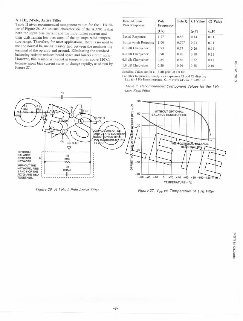
A 1 Hz, 2-Pole, Active FilterTable II gives recommended component values for the 1 Hz fil-ter of Figure 26. An unusual characteristic of the AD705 is thatboth the input bias current and the input offset current andtheir drift remain low over most of the op amps rated tempera-ture range. Therefore, for most applications, there is no need touse the normal balancing resistor tied between the noninvertingterminal of the op amp and ground. Eliminating the standardbalancing resistor reduces board space and lowers circuit noise.However, this resistor is needed at temperatures above 110°C,because input bias current starts to change rapidly, as shown byFigure 27.
C1
R11MQ
CAPACITORS C1, C2,AND C3 ARE SOUTHERNELECTRONICS MPCC,POLYCARBONATE, i5%,50 VOLT
R21MQ
INPUTOUTPUT
OPTIONAL ,- - - - - - - - - - - - - - - - - - - - - -,BALANCE: R3 :RESISTOR-, 2MQ ,NETWORK I ,
, IWITHOUTTHE: C3 :NETWORK,PINS, 0.0111F ,2 AND 6 OF THE' I
AD705ARETIED: :TOGETHER. ------------------------
Figure 26. A 1 Hz, 2-Pole Active Filter
--
Specified Values are for a - 3 dB point of 1.0 Hz.
For other frequencies, simply scalecapacitors Cl and C2 directly;i.e., for 3 Hz Bessel response,Cl = 0.046 fLF, C2 = 0.037 fLF.
Table II. Recommended Component Values for the 1HzLow Pass Filter
~I
i= 60!;.~:5ua: 30Ua:w~u::u...0w
~ -30~0>
Iii -60Cf)u...u...0
-8-
90
0
WITH OPTIONAL BALANCERESISTOR, R3
-90-60 -40 -20 0 +20 +40 +60 +80 +100 +120 +140
TEMPERATURE - °C
Figure 27. Vas vs. Temperature of 1Hz Filter
-----
aQ?
JN,.!.I!)MU
<iuj:JZ
CJwI-Za:a.
Desired Low Pole Pole Q CI Value C2 ValuePass Response Frequency
(Hz) (I-tF) (I-tF)
BesselResponse 1.27 0.58 0.14 O.ll
Butterworth Response 1.00 0.707 0.23 O.ll
0.1 dB Chebychev 0.93 0.77 0.26 0.11
0.2 dB Chebychev 0.90 0.80 0.28 O.ll
0.5 dB Chebychev 0.85 0.86 0.32 O.ll
1.0 dB Chebychev 0.80 0.96 0.38 0.10--
OBSOLETE