Embed Size (px)
Citation preview
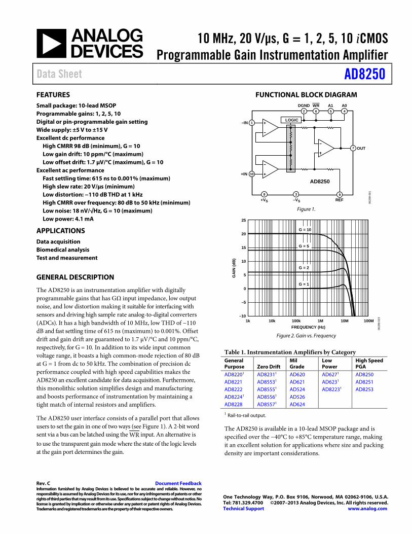
10 MHz, 20 V/μs, G = 1, 2, 5, 10 iCMOS Programmable Gain Instrumentation Amplifier
Data Sheet AD8250
Rev. C Document Feedback Information furnished by Analog Devices is believed to be accurate and reliable. However, no responsibility is assumed by Analog Devices for its use, nor for any infringements of patents or other rights of third parties that may result from its use. Specifications subject to change without notice. No license is granted by implication or otherwise under any patent or patent rights of Analog Devices. Trademarks and registered trademarks are the property of their respective owners.
One Technology Way, P.O. Box 9106, Norwood, MA 02062-9106, U.S.A. Tel: 781.329.4700 ©2007–2013 Analog Devices, Inc. All rights reserved. Technical Support www.analog.com
FEATURES Small package: 10-lead MSOP Programmable gains: 1, 2, 5, 10 Digital or pin-programmable gain setting Wide supply: ±5 V to ±15 V Excellent dc performance
High CMRR 98 dB (minimum), G = 10 Low gain drift: 10 ppm/°C (maximum) Low offset drift: 1.7 μV/°C (maximum), G = 10
Excellent ac performance Fast settling time: 615 ns to 0.001% (maximum) High slew rate: 20 V/µs (minimum) Low distortion: −110 dB THD at 1 kHz High CMRR over frequency: 80 dB to 50 kHz (minimum) Low noise: 18 nV/√Hz, G = 10 (maximum) Low power: 4.1 mA
APPLICATIONS Data acquisition Biomedical analysis Test and measurement
GENERAL DESCRIPTION
The AD8250 is an instrumentation amplifier with digitally programmable gains that has GΩ input impedance, low output noise, and low distortion making it suitable for interfacing with sensors and driving high sample rate analog-to-digital converters (ADCs). It has a high bandwidth of 10 MHz, low THD of −110 dB and fast settling time of 615 ns (maximum) to 0.001%. Offset drift and gain drift are guaranteed to 1.7 μV/°C and 10 ppm/°C, respectively, for G = 10. In addition to its wide input common voltage range, it boasts a high common-mode rejection of 80 dB at G = 1 from dc to 50 kHz. The combination of precision dc performance coupled with high speed capabilities makes the AD8250 an excellent candidate for data acquisition. Furthermore, this monolithic solution simplifies design and manufacturing and boosts performance of instrumentation by maintaining a tight match of internal resistors and amplifiers.
The AD8250 user interface consists of a parallel port that allows users to set the gain in one of two ways (see Figure 1). A 2-bit word sent via a bus can be latched using the WR input. An alternative is to use the transparent gain mode where the state of the logic levels at the gain port determines the gain.
FUNCTIONAL BLOCK DIAGRAM A1 A0DGND WR
AD8250
+VS –VS REF
OUT
+IN
LOGIC–IN
0628
8-00
1
1
10
8 3
7
4562
9
Figure 1.
25
–10
–5
0
5
10
15
20
1k 10k 100k 1M 10M 100M
GA
IN (d
B)
FREQUENCY (Hz)
G = 10
G = 5
G = 2
G = 1
0628
8-02
3
Figure 2. Gain vs. Frequency
Table 1. Instrumentation Amplifiers by Category General Purpose Zero Drift
Mil Grade
Low Power
High Speed PGA
AD82201 AD82311 AD620 AD6271 AD8250 AD8221 AD85531 AD621 AD6231 AD8251 AD8222 AD85551 AD524 AD82231 AD8253 AD82241 AD85561 AD526 AD8228 AD85571 AD624
1 Rail-to-rail output.
The AD8250 is available in a 10-lead MSOP package and is specified over the −40°C to +85°C temperature range, making it an excellent solution for applications where size and packing density are important considerations.
AD8250 Data Sheet
Rev. C | Page 2 of 24
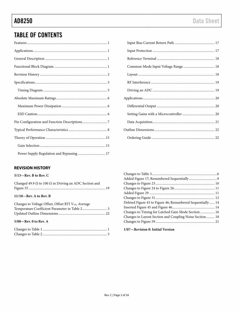
TABLE OF CONTENTS Features .............................................................................................. 1
Applications ....................................................................................... 1
General Description ......................................................................... 1
Functional Block Diagram .............................................................. 1
Revision History ............................................................................... 2
Specifications ..................................................................................... 3
Timing Diagram ........................................................................... 5
Absolute Maximum Ratings ............................................................ 6
Maximum Power Dissipation ..................................................... 6
ESD Caution .................................................................................. 6
Pin Configuration and Function Descriptions ............................. 7
Typical Performance Characteristics ............................................. 8
Theory of Operation ...................................................................... 15
Gain Selection ............................................................................. 15
Power Supply Regulation and Bypassing ................................ 17
Input Bias Current Return Path ............................................... 17
Input Protection ......................................................................... 17
Reference Terminal .................................................................... 18
Common-Mode Input Voltage Range ..................................... 18
Layout .......................................................................................... 18
RF Interference ........................................................................... 19
Driving an ADC ......................................................................... 19
Applications ..................................................................................... 20
Differential Output .................................................................... 20
Setting Gains with a Microcontroller ...................................... 20
Data Acquisition ......................................................................... 21
Outline Dimensions ....................................................................... 22
Ordering Guide .......................................................................... 22
REVISION HISTORY
5/13—Rev. B to Rev. C
Changed 49.9 Ω to 100 Ω in Driving an ADC Section and Figure 55 .......................................................................................... 19
11/10—Rev. A to Rev. B
Changes to Voltage Offset, Offset RTI VOS, Average Temperature Coefficient Parameter in Table 2 ............................. 3 Updated Outline Dimensions ....................................................... 22
5/08—Rev. 0 to Rev. A
Changes to Table 1 ............................................................................ 1 Changes to Table 2 ............................................................................ 3
Changes to Table 3 ............................................................................. 6 Added Figure 17; Renumbered Sequentially ................................. 9 Changes to Figure 23 ...................................................................... 10 Changes to Figure 24 to Figure 26 ................................................ 11 Added Figure 29 ............................................................................. 11 Changes to Figure 31 ...................................................................... 12 Deleted Figure 43 to Figure 46; Renumbered Sequentially ...... 14 Inserted Figure 45 and Figure 46 .................................................. 14 Changes to Timing for Latched Gain Mode Section ................. 16 Changes to Layout Section and Coupling Noise Section .......... 18 Changes to Figure 59 ...................................................................... 21
1/07—Revision 0: Initial Version
Data Sheet AD8250
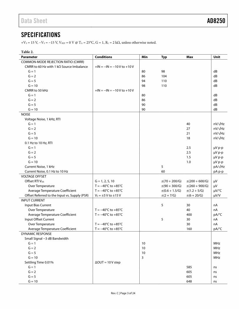
Rev. C | Page 3 of 24
SPECIFICATIONS +VS = 15 V, −VS = −15 V, VREF = 0 V @ TA = 25°C, G = 1, RL = 2 kΩ, unless otherwise noted.
Table 2. Parameter Conditions Min Typ Max Unit COMMON-MODE REJECTION RATIO (CMRR)
CMRR to 60 Hz with 1 kΩ Source Imbalance +IN = −IN = −10 V to +10 V G = 1 80 98 dB G = 2 86 104 dB G = 5 94 110 dB G = 10 98 110 dB
CMRR to 50 kHz +IN = −IN = −10 V to +10 V G = 1 80 dB G = 2 86 dB G = 5 90 dB G = 10 90 dB
NOISE Voltage Noise, 1 kHz, RTI
G = 1 40 nV/√Hz G = 2 27 nV/√Hz G = 5 21 nV/√Hz G = 10 18 nV/√Hz
0.1 Hz to 10 Hz, RTI G = 1 2.5 μV p-p G = 2 2.5 μV p-p G = 5 1.5 μV p-p G = 10 1.0 μV p-p
Current Noise, 1 kHz 5 pA/√Hz Current Noise, 0.1 Hz to 10 Hz 60 pA p-p
VOLTAGE OFFSET Offset RTI VOS G = 1, 2, 5, 10 ±(70 + 200/G) ±(200 + 600/G) μV
Over Temperature T = −40°C to +85°C ±(90 + 300/G) ±(260 + 900/G) μV Average Temperature Coefficient T = −40°C to +85°C ±(0.6 + 1.5/G) ±(1.2 + 5/G) μV/°C
Offset Referred to the Input vs. Supply (PSR) VS = ±5 V to ±15 V ±(2 + 7/G) ±(6 + 20/G) μV/V INPUT CURRENT
Input Bias Current 5 30 nA Over Temperature T = −40°C to +85°C 40 nA Average Temperature Coefficient T = −40°C to +85°C 400 pA/°C
Input Offset Current 5 30 nA Over Temperature T = −40°C to +85°C 30 nA Average Temperature Coefficient T = −40°C to +85°C 160 pA/°C
DYNAMIC RESPONSE Small Signal −3 dB Bandwidth
G = 1 10 MHz G = 2 10 MHz G = 5 10 MHz G = 10 3 MHz
Settling Time 0.01% ΔOUT = 10 V step G = 1 585 ns G = 2 605 ns G = 5 605 ns G = 10 648 ns
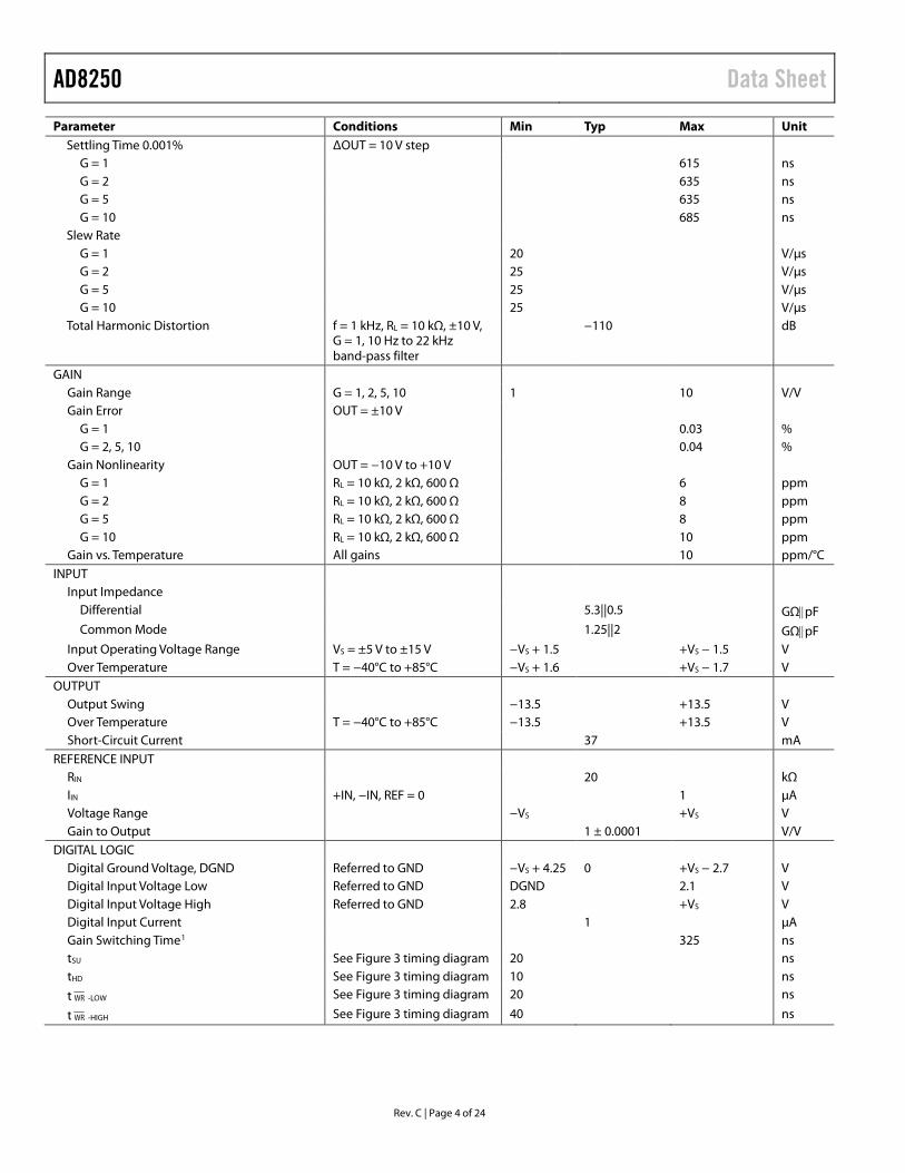
AD8250 Data Sheet
Rev. C | Page 4 of 24
Parameter Conditions Min Typ Max Unit Settling Time 0.001% ΔOUT = 10 V step
G = 1 615 ns G = 2 635 ns G = 5 635 ns G = 10 685 ns
Slew Rate G = 1 20 V/μs G = 2 25 V/μs G = 5 25 V/μs G = 10 25 V/μs
Total Harmonic Distortion f = 1 kHz, RL = 10 kΩ, ±10 V, G = 1, 10 Hz to 22 kHz band-pass filter
−110 dB
GAIN Gain Range G = 1, 2, 5, 10 1 10 V/V Gain Error OUT = ±10 V
G = 1 0.03 % G = 2, 5, 10 0.04 %
Gain Nonlinearity OUT = −10 V to +10 V G = 1 RL = 10 kΩ, 2 kΩ, 600 Ω 6 ppm G = 2 RL = 10 kΩ, 2 kΩ, 600 Ω 8 ppm G = 5 RL = 10 kΩ, 2 kΩ, 600 Ω 8 ppm G = 10 RL = 10 kΩ, 2 kΩ, 600 Ω 10 ppm
Gain vs. Temperature All gains 10 ppm/°C INPUT
Input Impedance Differential 5.3||0.5 GΩ||pF Common Mode 1.25||2 GΩ||pF
Input Operating Voltage Range VS = ±5 V to ±15 V −VS + 1.5 +VS − 1.5 V Over Temperature T = −40°C to +85°C −VS + 1.6 +VS − 1.7 V
OUTPUT Output Swing −13.5 +13.5 V Over Temperature T = −40°C to +85°C −13.5 +13.5 V Short-Circuit Current 37 mA
REFERENCE INPUT RIN 20 kΩ IIN +IN, −IN, REF = 0 1 μA Voltage Range −VS +VS V Gain to Output 1 ± 0.0001 V/V
DIGITAL LOGIC Digital Ground Voltage, DGND Referred to GND −VS + 4.25 0 +VS − 2.7 V Digital Input Voltage Low Referred to GND DGND 2.1 V Digital Input Voltage High Referred to GND 2.8 +VS V Digital Input Current 1 μA Gain Switching Time1 325 ns tSU See Figure 3 timing diagram 20 ns tHD See Figure 3 timing diagram 10 ns
t WR -LOW See Figure 3 timing diagram 20 ns
t WR -HIGH See Figure 3 timing diagram 40 ns
Data Sheet AD8250
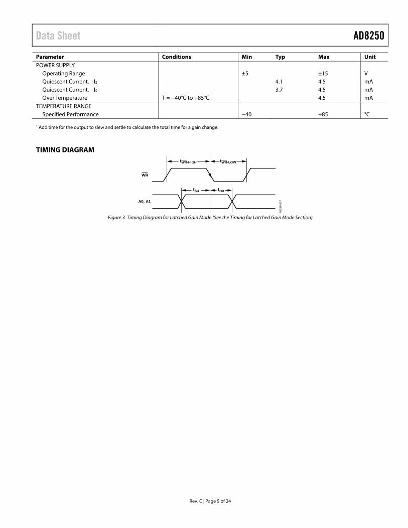
Rev. C | Page 5 of 24
Parameter Conditions Min Typ Max Unit POWER SUPPLY
Operating Range ±5 ±15 V Quiescent Current, +IS 4.1 4.5 mA Quiescent Current, −IS 3.7 4.5 mA Over Temperature T = −40°C to +85°C 4.5 mA
TEMPERATURE RANGE Specified Performance −40 +85 °C
1 Add time for the output to slew and settle to calculate the total time for a gain change.
TIMING DIAGRAM
A0, A1
WR
tSU tHD
tWR-HIGH tWR-LOW
0628
8-05
7
Figure 3. Timing Diagram for Latched Gain Mode (See the Timing for Latched Gain Mode Section)
AD8250 Data Sheet
Rev. C | Page 6 of 24
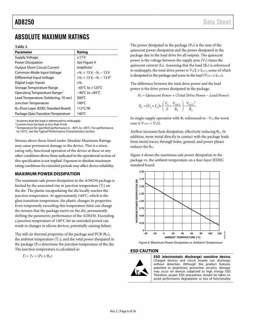
ABSOLUTE MAXIMUM RATINGS Table 3. Parameter Rating Supply Voltage ±17 V Power Dissipation See Figure 4 Output Short-Circuit Current Indefinite1 Common-Mode Input Voltage +VS + 13 V, −VS − 13 V Differential Input Voltage +VS + 13 V, −VS − 13 V2 Digital Logic Inputs ±VS Storage Temperature Range −65°C to +125°C Operating Temperature Range3 −40°C to +85°C Lead Temperature (Soldering, 10 sec) 300°C Junction Temperature 140°C
θJA (Four-Layer JEDEC Standard Board) 112°C/W
Package Glass Transition Temperature 140°C
1 Assumes that the load is referenced to midsupply. 2 Current must be kept to less than 6 mA. 3 Temperature for specified performance is −40°C to +85°C. For performance
to 125°C, see the Typical Performance Characteristics section.
Stresses above those listed under Absolute Maximum Ratings may cause permanent damage to the device. This is a stress rating only; functional operation of the device at these or any other conditions above those indicated in the operational section of this specification is not implied. Exposure to absolute maximum rating conditions for extended periods may affect device reliability.
MAXIMUM POWER DISSIPATION The maximum safe power dissipation in the AD8250 package is limited by the associated rise in junction temperature (TJ) on the die. The plastic encapsulating the die locally reaches the junction temperature. At approximately 140°C, which is the glass transition temperature, the plastic changes its properties. Even temporarily exceeding this temperature limit can change the stresses that the package exerts on the die, permanently shifting the parametric performance of the AD8250. Exceeding a junction temperature of 140°C for an extended period can result in changes in silicon devices, potentially causing failure.
The still-air thermal properties of the package and PCB (θJA), the ambient temperature (TA), and the total power dissipated in the package (PD) determine the junction temperature of the die. The junction temperature is calculated as
TJ = TA + (PD × θJA)
The power dissipated in the package (PD) is the sum of the quiescent power dissipation and the power dissipated in the package due to the load drive for all outputs. The quiescent power is the voltage between the supply pins (VS) times the quiescent current (IS). Assuming that the load (RL) is referenced to midsupply, the total drive power is VS/2 × IOUT, some of which is dissipated in the package and some in the load (VOUT × IOUT).
The difference between the total drive power and the load power is the drive power dissipated in the package.
PD = Quiescent Power + (Total Drive Power − Load Power)
( )L
OUT
L
OUTSSSD R
VR
VVIVP
2
–2
×+×=
In single-supply operation with RL referenced to −VS, the worst case is VOUT = VS/2.
Airflow increases heat dissipation, effectively reducing θJA. In addition, more metal directly in contact with the package leads from metal traces, through holes, ground, and power planes reduces the θJA.
Figure 4 shows the maximum safe power dissipation in the package vs. the ambient temperature on a four-layer JEDEC standard board.
2.00
1.75
1.50
1.25
1.00
0.75
0.50
0.25
0–40 –20 120100806040200
MA
XIM
UM
PO
WER
DIS
SIPA
TIO
N (W
)
AMBIENT TEMPERATURE (°C) 0628
8-00
4
Figure 4. Maximum Power Dissipation vs. Ambient Temperature
ESD CAUTION
Data Sheet AD8250
Rev. C | Page 7 of 24
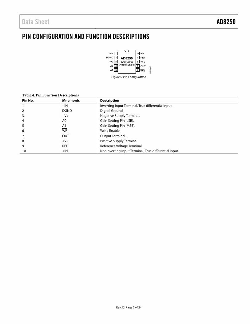
PIN CONFIGURATION AND FUNCTION DESCRIPTIONS
–INDGND
–VS
A0A1
+IN
REF+VS
OUT
WR
AD8250TOP VIEW
(Not to Scale)
1
2
3
4
5
10
9
8
7
6
0628
8-00
5
Figure 5. Pin Configuration
Table 4. Pin Function Descriptions Pin No. Mnemonic Description 1 −IN Inverting Input Terminal. True differential input. 2 DGND Digital Ground. 3 −VS Negative Supply Terminal. 4 A0 Gain Setting Pin (LSB). 5 A1 Gain Setting Pin (MSB). 6 WR Write Enable.
7 OUT Output Terminal. 8 +VS Positive Supply Terminal. 9 REF Reference Voltage Terminal. 10 +IN Noninverting Input Terminal. True differential input.
AD8250 Data Sheet
Rev. C | Page 8 of 24
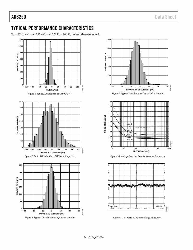
TYPICAL PERFORMANCE CHARACTERISTICS TA = 25°C, +VS = +15 V, −VS = −15 V, RL = 10 kΩ, unless otherwise noted.
0628
8-00
6
1400
1200
800
1000
600
400
200
0
NU
MB
ER O
F U
NIT
S
CMRR (µV/V)–120 –90 –60 –30 0 30 60 90 120
Figure 6. Typical Distribution of CMRR, G = 1
300
350
250
200
150
100
50
0–200 2001000–100 –50 50–150 150
NU
MB
ER O
F U
NIT
S
OFFSET VOLTAGE RTI (µV) 0628
8-00
7
Figure 7. Typical Distribution of Offset Voltage, VOSI
600
500
400
300
200
100
0–30 3010 200–10–20
NU
MB
ER O
F U
NIT
S
INPUT BIAS CURRENT (nA) 0628
8-00
8
Figure 8. Typical Distribution of Input Bias Current
500
400
300
200
100
0–30 3020100–20 –10
NU
MB
ER O
F U
NIT
S
INPUT OFFSET CURRENT (nA) 0628
8-00
9
Figure 9. Typical Distribution of Input Offset Current
90
0
10
20
30
40
50
60
70
80
1 10 100 1k 10k 100k
0628
8-01
0
NO
ISE
RTI
(nV/
Hz)
FREQUENCY (Hz)
G = 1
G = 2
G = 5
G = 10
Figure 10. Voltage Spectral Density Noise vs. Frequency
0628
8-01
11s/DIV2µV/DIV
Figure 11. 0.1 Hz to 10 Hz RTI Voltage Noise, G = 1
Data Sheet AD8250
Rev. C | Page 9 of 24
0628
8-01
21s/DIV1µV/DIV
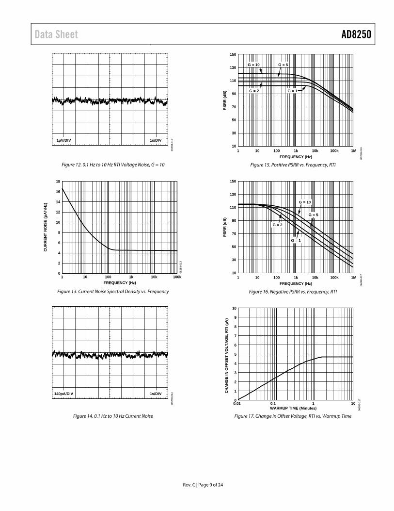
Figure 12. 0.1 Hz to 10 Hz RTI Voltage Noise, G = 10
18
0
2
4
6
8
10
12
14
16
1 10 100 1k 10k 100k
0628
8-01
3
CU
RR
ENT
NO
ISE
(pA
/ H
z)
FREQUENCY (Hz) Figure 13. Current Noise Spectral Density vs. Frequency
0628
8-01
41s/DIV140pA/DIV
Figure 14. 0.1 Hz to 10 Hz Current Noise
150
130
110
90
70
50
30
101 10 100 1k 10k 100k 1M
PSR
R (d
B)
FREQUENCY (Hz)
G = 10 G = 5
G = 2 G = 1
0628
8-01
6
Figure 15. Positive PSRR vs. Frequency, RTI
150
130
110
90
70
50
30
101 10 100 1k 10k 100k 1M
PSR
R (d
B)
FREQUENCY (Hz)
G = 10
G = 5
G = 2
G = 1
0628
8-01
7
Figure 16. Negative PSRR vs. Frequency, RTI
10
9
8
7
6
5
4
3
2
1
010
CH
AN
GE
IN O
FFSE
T VO
LTA
GE,
RTI
(µV)
0.01 0.1 1WARMUP TIME (Minutes) 06
288-
117
Figure 17. Change in Offset Voltage, RTI vs. Warmup Time
AD8250 Data Sheet
Rev. C | Page 10 of 24
15
10
5
0
–5
–10
–15–40 –25 –10 5 20 35 50 65 80 95 110 125
IB–
IB+
IOS
INP
UT
BIA
S C
UR
RE
NT
AN
D O
FF
SE
T C
UR
RE
NT
(n
A)
TEMPERATURE (°C) 0628
8-01
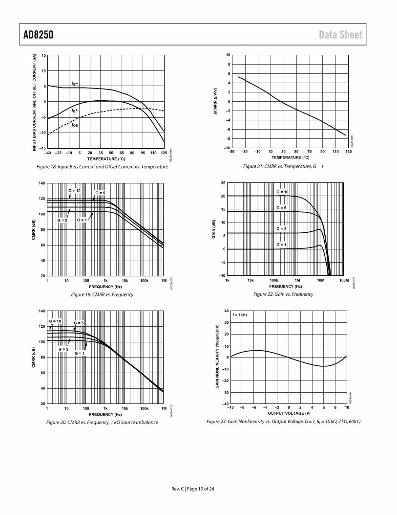
9Figure 18. Input Bias Current and Offset Current vs. Temperature
140
120
100
80
60
40
201 10 100 1k 10k 100k 1M
CM
RR
(d
B)
FREQUENCY (Hz)
G = 10G = 5
G = 2 G = 1
0628
8-02
0
Figure 19. CMRR vs. Frequency
140
120
100
80
60
40
201 10 100 1k 10k 100k 1M
CM
RR
(d
B)
FREQUENCY (Hz)
G = 10 G = 5
G = 2G = 1
0628
8-02
1
Figure 20. CMRR vs. Frequency, 1 kΩ Source Imbalance
10
–10
–8
–6
–4
–2
0
2
4
6
8
–50 –30 –10 10 30 50 70 90 110 130
0628
8-04
9
∆C
MR
R (
µV
/V)
TEMPERATURE (°C)
Figure 21. CMRR vs. Temperature, G = 1
25
–10
–5
0
5
10
15
20
1k 10k 100k 1M 10M 100M
GA
IN (
dB
)
FREQUENCY (Hz)
G = 10
G = 5
G = 2
G = 1
0628
8-02
3
Figure 22. Gain vs. Frequency
40
30
20
10
–10
–30
0
–20
–40–10 –8 –6 –4 –2 0 2 4 6 8 10
0628
8-02
4
GA
IN N
ON
LIN
EA
RIT
Y (
10p
pm
/DIV
)
OUTPUT VOLTAGE (V)
f = 1kHz
Figure 23. Gain Nonlinearity vs. Output Voltage, G = 1, RL = 10 kΩ, 2 kΩ, 600 Ω
Data Sheet AD8250
Rev. C | Page 11 of 24
–10 –8 –6 –4 –2 0 2 4 6 8 10
0628
8-02
5
OUTPUT VOLTAGE (V)
f = 1kHz40
30
20
10
–10
–30
0
–20
–40
GA
IN N
ON
LIN
EAR
ITY
(10p
pm/D
IV)
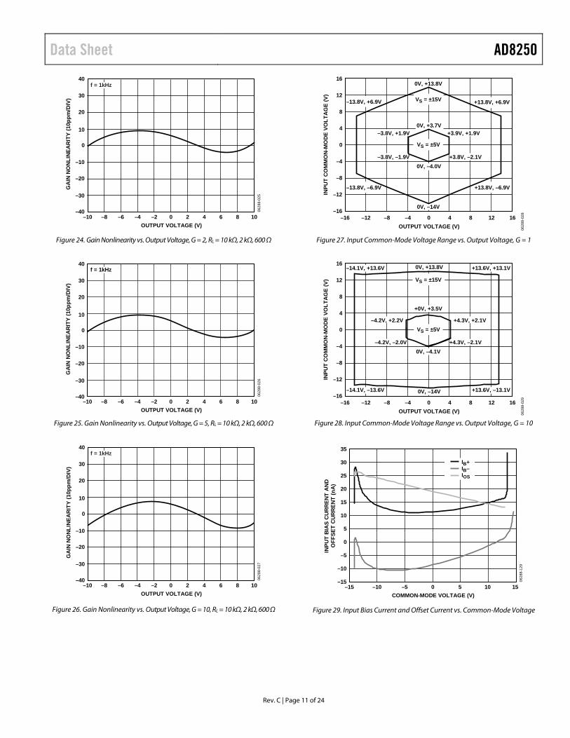
Figure 24. Gain Nonlinearity vs. Output Voltage, G = 2, RL = 10 kΩ, 2 kΩ, 600 Ω
–10 –8 –6 –4 –2 0 2 4 6 8 10
0628
8-02
6
OUTPUT VOLTAGE (V)
f = 1kHz40
30
20
10
–10
–30
0
–20
–40
GA
IN N
ON
LIN
EAR
ITY
(10p
pm/D
IV)
Figure 25. Gain Nonlinearity vs. Output Voltage, G = 5, RL = 10 kΩ, 2 kΩ, 600 Ω
–10 –8 –6 –4 –2 0 2 4 6 8 10
0628
8-02
7
OUTPUT VOLTAGE (V)
f = 1kHz40
30
20
10
–10
–30
0
–20
–40
GA
IN N
ON
LIN
EAR
ITY
(10p
pm/D
IV)
Figure 26. Gain Nonlinearity vs. Output Voltage, G = 10, RL = 10 kΩ, 2 kΩ, 600 Ω
16
–16
–12
–8
–4
0
4
8
12
–16 –12 –8 –4 0 4 8 12 16
INPU
T C
OM
MO
N-M
OD
E VO
LTA
GE
(V)
OUTPUT VOLTAGE (V)
VS = ±15V–13.8V, +6.9V
–13.8V, –6.9V +13.8V, –6.9V
+13.8V, +6.9V
–3.8V, +1.9V
–3.8V, –1.9V
+3.9V, +1.9V0V, +3.7V
0V, –4.0V+3.8V, –2.1V
0V, +13.8V
0V, –14V
VS = ±5V
0628
8-02
8
Figure 27. Input Common-Mode Voltage Range vs. Output Voltage, G = 1
16
–16
–12
–8
–4
0
4
8
12
–16 –12 –8 –4 0 4 8 12 16
INPU
T C
OM
MO
N-M
OD
E VO
LTA
GE
(V)
OUTPUT VOLTAGE (V)
VS = ±15V
–14.1V, +13.6V
–4.2V, +2.2V +4.3V, +2.1V
+4.3V, –2.1V–4.2V, –2.0V0V, –4.1V
+0V, +3.5V
0V, –14V
0V, +13.8V
–14.1V, –13.6V
+13.6V, +13.1V
+13.6V, –13.1V
VS = ±5V
0628
8-02
9
Figure 28. Input Common-Mode Voltage Range vs. Output Voltage, G = 10
35
30
25
20
15
10
5
0
–5
–10
–15–15 –10 –5 0 5 10 15
0628
8-12
9
INPU
T B
IAS
CU
RR
ENT
AN
DO
FFSE
T C
UR
REN
T (n
A)
COMMON-MODE VOLTAGE (V)
IB+IB–IOS
Figure 29. Input Bias Current and Offset Current vs. Common-Mode Voltage
AD8250 Data Sheet
Rev. C | Page 12 of 24
+VS
–VS
+1
+2
–2
–1
4 6 8 10 12 14 16
–40°C
–40°C
+25°C
+25°C
+85°C
+85°C
+125°C
INP
UT
VO
LT
AG
ER
EF
ER
RE
D T
O S
UP
PL
Y V
OL
TA
GE
(V
)
SUPPLY VOLTAGE (±VS)
+125°C
0628
8-03
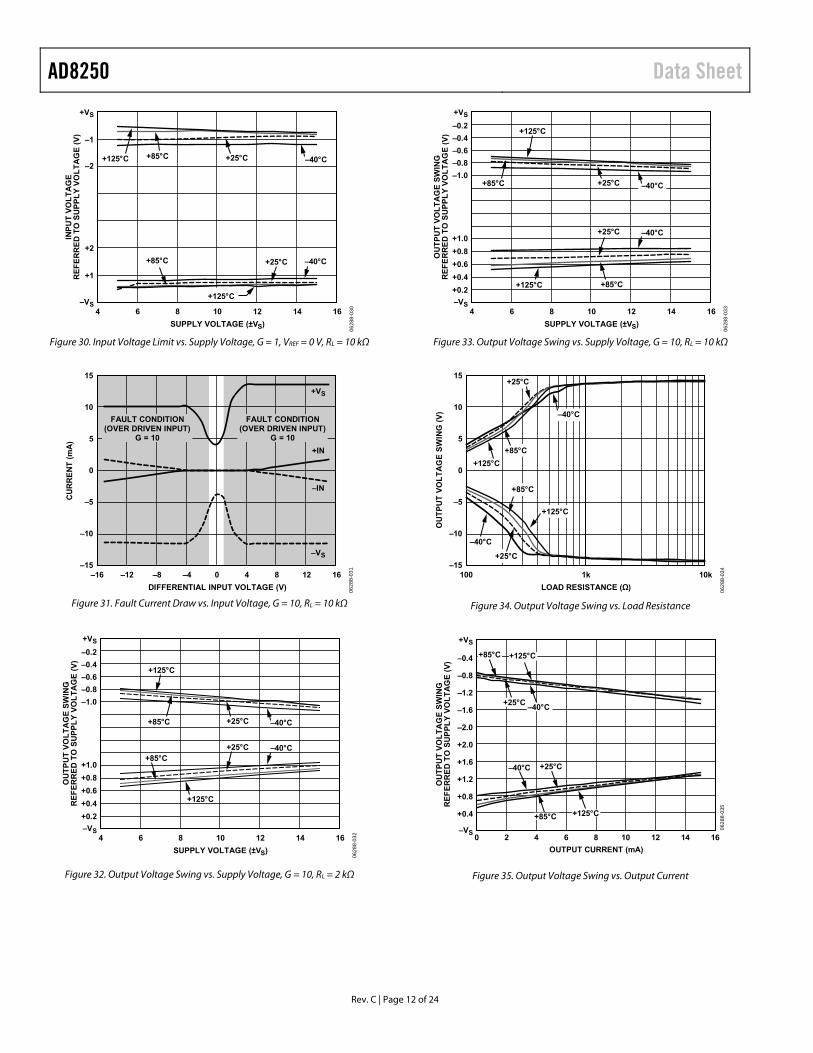
0Figure 30. Input Voltage Limit vs. Supply Voltage, G = 1, VREF = 0 V, RL = 10 kΩ
15
–15
–10
–5
0
5
10
–16 –12 –8 –4 0 4 8 12 16
+VS
+IN
–IN
–VS
CU
RR
EN
T (
mA
)
DIFFERENTIAL INPUT VOLTAGE (V) 0628
8-03
1
FAULT CONDITION(OVER DRIVEN INPUT)
G = 10
FAULT CONDITION(OVER DRIVEN INPUT)
G = 10
Figure 31. Fault Current Draw vs. Input Voltage, G = 10, RL = 10 kΩ
+VS
–VS
+0.2
+0.4
+0.6
+0.8
+1.0
–1.0
–0.8
–0.6
–0.4
–0.2
4 6 8 10 12 14 16
OU
TP
UT
VO
LT
AG
E S
WIN
GR
EF
ER
RE
D T
O S
UP
PL
Y V
OL
TA
GE
(V
)
SUPPLY VOLTAGE (±VS)
–40°C
–40°C
+25°C
+25°C
+85°C
+85°C
+125°C
+125°C
0628
8-03
2
Figure 32. Output Voltage Swing vs. Supply Voltage, G = 10, RL = 2 kΩ
+VS
–VS
+0.2
+0.4
+0.6
+0.8
+1.0
–1.0
–0.8
–0.6
–0.4
–0.2
4 6 8 10 12 14 16
OU
TP
UT
VO
LT
AG
E S
WIN
GR
EF
ER
RE
D T
O S
UP
PL
Y V
OL
TA
GE
(V
)
SUPPLY VOLTAGE (±VS)
–40°C
+25°C
+25°C
+85°C
+85°C
+125°C
+125°C
–40°C
0628
8-03
3
Figure 33. Output Voltage Swing vs. Supply Voltage, G = 10, RL = 10 kΩ
15
10
5
0
–5
–10
–15100 1k 10k
OU
TP
UT
VO
LT
AG
E S
WIN
G (
V)
LOAD RESISTANCE (Ω)
+125°C
–40°C
–40°C
+85°C
+85°C
+25°C
+25°C
+125°C
0628
8-03
4
Figure 34. Output Voltage Swing vs. Load Resistance
+VS
–0.8
–0.4
–2.0
–1.6
–1.2
+1.2
+1.6
+2.0
+0.8
+0.4
–VS0 2 6 10 144 8 12 16
0628
8-03
5
OU
TP
UT
VO
LT
AG
E S
WIN
GR
EF
ER
RE
D T
O S
UP
PL
Y V
OL
TA
GE
(V
)
OUTPUT CURRENT (mA)
+125°C+85°C
+25°C–40°C
+125°C+85°C
+25°C–40°C
Figure 35. Output Voltage Swing vs. Output Current
Data Sheet AD8250
Rev. C | Page 13 of 24
V OU
T (V
)
TIME (µs)
2µs/DIV20mV/DIV
NOLOAD 47pF
100pF
0628
8-03
6
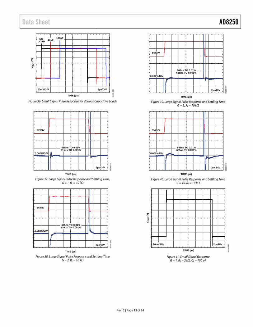
Figure 36. Small Signal Pulse Response for Various Capacitive Loads
0628
8-03
7
5V/DIV
2µs/DIV
TIME (µs)
0.002%/DIV
585ns TO 0.01%615ns TO 0.001%
Figure 37. Large Signal Pulse Response and Settling Time,
G = 1, RL = 10 kΩ
0628
8-03
8
5V/DIV
2µs/DIV
TIME (µs)
0.002%/DIV
605ns TO 0.01%635ns TO 0.001%
Figure 38. Large Signal Pulse Response and Settling Time
G = 2, RL = 10 kΩ
0628
8-03
9
5V/DIV
2µs/DIV
TIME (µs)
0.002%/DIV
605ns TO 0.01%635ns TO 0.001%
Figure 39. Large Signal Pulse Response and Settling Time
G = 5, RL = 10 kΩ
0628
8-04
0
5V/DIV
2µs/DIV
TIME (µs)
0.002%/DIV
648ns TO 0.01%685ns TO 0.001%
Figure 40. Large Signal Pulse Response and Settling Time
G = 10, RL = 10 kΩ
V OU
T (V
)
TIME (µs)
2µs/DIV20mV/DIV
0628
8-04
2
Figure 41. Small Signal Response G = 1, RL = 2 kΩ, CL = 100 pF
AD8250 Data Sheet
Rev. C | Page 14 of 24
V OU
T (V
)
TIME (µs)
2µs/DIV20mV/DIV
0628
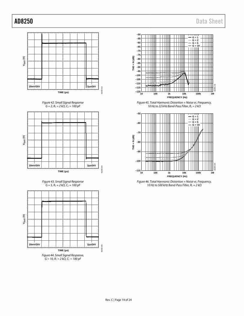
8-04
3
Figure 42. Small Signal Response G = 2, RL = 2 kΩ, CL = 100 pF
V OU
T (V
)
TIME (µs)
2µs/DIV20mV/DIV
0628
8-04
4
Figure 43. Small Signal Response G = 5, RL = 2 kΩ, CL = 100 pF
V OU
T (V
)
TIME (µs)
2µs/DIV20mV/DIV
0628
8-04
5
Figure 44. Small Signal Response,
G = 10, RL = 2 kΩ, CL = 100 pF
–50–55–60–65–70–75–80–85–90–95
–100–105–110–115–120
10 100 1k 10k 100k 1M
0628
8-14
9
THD
+ N
(dB
)
FREQUENCY (Hz)
G = 1G = 2G = 5G = 10
Figure 45. Total Harmonic Distortion + Noise vs. Frequency,
10 Hz to 22 kHz Band-Pass Filter, RL = 2 kΩ
–50
–60
–70
–80
–90
–100
–11010 100 1k 10k 100k 1M
0628
8-15
0
FREQUENCY (Hz)
G = 1G = 2G = 5G = 10
THD
+ N
(dB
)
Figure 46. Total Harmonic Distortion + Noise vs. Frequency,
10 Hz to 500 kHz Band-Pass Filter, RL = 2 kΩ
Data Sheet AD8250
Rev. C | Page 15 of 24
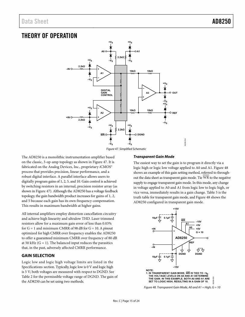
THEORY OF OPERATION
10kΩ
10kΩ 10kΩ
10kΩREF
OUTA3
–IN
+IN
WR
2.2kΩ
2.2kΩ
+VS +VS
–VS –VS
+VS
–VS+VS
–VS
A1A0
2.2kΩ
DGND
A1
A2
DIGITALGAINCONTROL
2.2kΩ
+VS
–VS
+VS
–VS
+VS
–VS
+VS
–VS
0628
8-05
4
Figure 47. Simplified Schematic
The AD8250 is a monolithic instrumentation amplifier based on the classic, 3-op-amp topology as shown in Figure 47. It is fabricated on the Analog Devices, Inc., proprietary iCMOS® process that provides precision, linear performance, and a robust digital interface. A parallel interface allows users to digitally program gains of 1, 2, 5, and 10. Gain control is achieved by switching resistors in an internal, precision resistor array (as shown in Figure 47). Although the AD8250 has a voltage feedback topology, the gain bandwidth product increases for gains of 1, 2, and 5 because each gain has its own frequency compensation. This results in maximum bandwidth at higher gains.
All internal amplifiers employ distortion cancellation circuitry and achieve high linearity and ultralow THD. Laser trimmed resistors allow for a maximum gain error of less than 0.03% for G = 1 and minimum CMRR of 98 dB for G = 10. A pinout optimized for high CMRR over frequency enables the AD8250 to offer a guaranteed minimum CMRR over frequency of 80 dB at 50 kHz (G = 1). The balanced input reduces the parasitics that, in the past, adversely affected CMRR performance.
GAIN SELECTION Logic low and logic high voltage limits are listed in the Specifications section. Typically, logic low is 0 V and logic high is 5 V; both voltages are measured with respect to DGND. See Table 2 for the permissible voltage range of DGND. The gain of the AD8250 can be set using two methods.
Transparent Gain Mode
The easiest way to set the gain is to program it directly via a logic high or logic low voltage applied to A0 and A1. Figure 48 shows an example of this gain setting method, referred to through-out the data sheet as transparent gain mode. Tie WR to the negative supply to engage transparent gain mode. In this mode, any change in voltage applied to A0 and A1 from logic low to logic high, or vice versa, immediately results in a gain change. Table 5 is the truth table for transparent gain mode, and Figure 48 shows the AD8250 configured in transparent gain mode.
+15V
–15V
–15V
A0
A1
WR
+IN
+5V
+5V
–IN
10μF 0.1µF
10μF 0.1µF
G = 10
DGND DGND
REF
AD8250
0628
8-05
5
NOTE:1. IN TRANSPARENT GAIN MODE, WR IS TIED TO −VS.
THE VOLTAGE LEVELS ON A0 AND A1 DETERMINETHE GAIN. IN THIS EXAMPLE, BOTH A0 AND A1 ARESET TO LOGIC HIGH, RESULTING IN A GAIN OF 10.
Figure 48. Transparent Gain Mode, A0 and A1 = High, G = 10
AD8250 Data Sheet
Rev. C | Page 16 of 24
Table 5. Truth Table Logic Levels for Transparent Gain Mode WR A1 A0 Gain
−VS Low Low 1 −VS Low High 2 −VS High Low 5 −VS High High 10
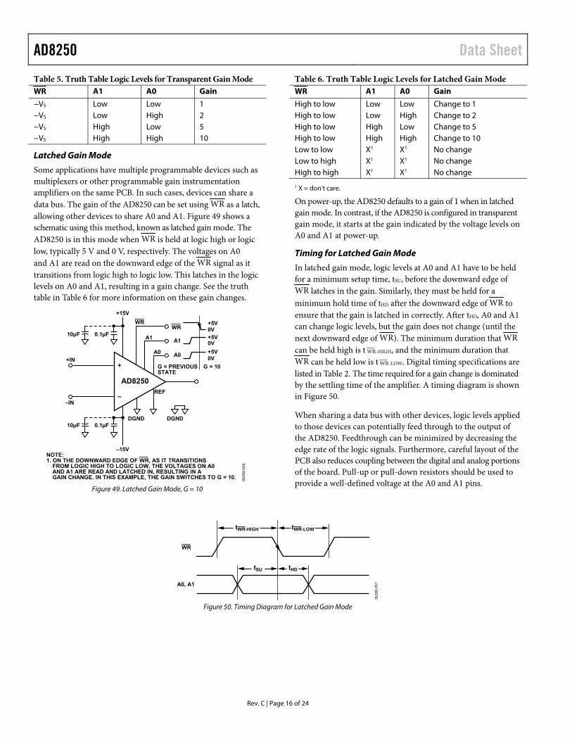
Latched Gain Mode
Some applications have multiple programmable devices such as multiplexers or other programmable gain instrumentation amplifiers on the same PCB. In such cases, devices can share a data bus. The gain of the AD8250 can be set using WR as a latch, allowing other devices to share A0 and A1. Figure 49 shows a schematic using this method, known as latched gain mode. The AD8250 is in this mode when WR is held at logic high or logic low, typically 5 V and 0 V, respectively. The voltages on A0 and A1 are read on the downward edge of the WR signal as it transitions from logic high to logic low. This latches in the logic levels on A0 and A1, resulting in a gain change. See the truth table in Table 6 for more information on these gain changes.
+15V
–15V
A0
A1
WR
+IN
–IN
10μF 0.1µF
10μF 0.1µFDGND DGND
REF
AD8250
A0
A1
WR
+5V
+5V
+5V0V
0V
0V
G = PREVIOUSSTATE
G = 10
0628
8-05
6
+
–
NOTE:1. ON THE DOWNWARD EDGE OF WR, AS IT TRANSITIONS
FROM LOGIC HIGH TO LOGIC LOW, THE VOLTAGES ON A0AND A1 ARE READ AND LATCHED IN, RESULTING IN AGAIN CHANGE. IN THIS EXAMPLE, THE GAIN SWITCHES TO G = 10.
Figure 49. Latched Gain Mode, G = 10
Table 6. Truth Table Logic Levels for Latched Gain Mode WR A1 A0 Gain
High to low Low Low Change to 1 High to low Low High Change to 2 High to low High Low Change to 5 High to low High High Change to 10 Low to low X1 X1 No change Low to high X1 X1 No change High to high X1 X1 No change
1 X = don’t care.
On power-up, the AD8250 defaults to a gain of 1 when in latched gain mode. In contrast, if the AD8250 is configured in transparent gain mode, it starts at the gain indicated by the voltage levels on A0 and A1 at power-up.
Timing for Latched Gain Mode
In latched gain mode, logic levels at A0 and A1 have to be held for a minimum setup time, tSU, before the downward edge of WR latches in the gain. Similarly, they must be held for a minimum hold time of tHD after the downward edge of WR to ensure that the gain is latched in correctly. After tHD, A0 and A1 can change logic levels, but the gain does not change (until the next downward edge of WR). The minimum duration that WR can be held high is t WR-HIGH, and the minimum duration that WR can be held low is t WR-LOW. Digital timing specifications are listed in Table 2. The time required for a gain change is dominated by the settling time of the amplifier. A timing diagram is shown in Figure 50.
When sharing a data bus with other devices, logic levels applied to those devices can potentially feed through to the output of the AD8250. Feedthrough can be minimized by decreasing the edge rate of the logic signals. Furthermore, careful layout of the PCB also reduces coupling between the digital and analog portions of the board. Pull-up or pull-down resistors should be used to provide a well-defined voltage at the A0 and A1 pins.
A0, A1
WR
tSU tHD
tWR-HIGH tWR-LOW
0628
8-05
7
Figure 50. Timing Diagram for Latched Gain Mode
Data Sheet AD8250
Rev. C | Page 17 of 24
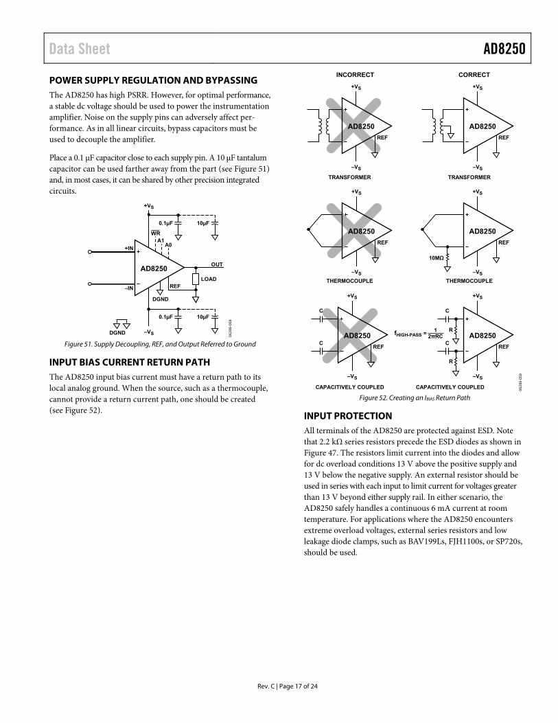
POWER SUPPLY REGULATION AND BYPASSING The AD8250 has high PSRR. However, for optimal performance, a stable dc voltage should be used to power the instrumentation amplifier. Noise on the supply pins can adversely affect per-formance. As in all linear circuits, bypass capacitors must be used to decouple the amplifier.
Place a 0.1 μF capacitor close to each supply pin. A 10 μF tantalum capacitor can be used farther away from the part (see Figure 51) and, in most cases, it can be shared by other precision integrated circuits.
AD8250
+VS
+IN
–IN
LOADREF
0.1µF 10µF
0.1µF 10µF
–VSDGND
OUT
DGND
A0A1
WR06
288-
058
Figure 51. Supply Decoupling, REF, and Output Referred to Ground
INPUT BIAS CURRENT RETURN PATH The AD8250 input bias current must have a return path to its local analog ground. When the source, such as a thermocouple, cannot provide a return current path, one should be created (see Figure 52).
THERMOCOUPLE
+VS
REF
–VS
AD8250
CAPACITIVELY COUPLED
+VS
REF
C
C
–VS
AD8250
TRANSFORMER
+VS
REF
–VS
AD8250
INCORRECT
CAPACITIVELY COUPLED
+VS
REF
C
R
R
C
–VS
AD82501fHIGH-PASS =
2πRC
THERMOCOUPLE
+VS
REF
–VS
10MΩ
AD8250
TRANSFORMER
+VS
REF
–VS
AD8250
CORRECT
0628
8-05
9
Figure 52. Creating an IBIAS Return Path
INPUT PROTECTION All terminals of the AD8250 are protected against ESD. Note that 2.2 kΩ series resistors precede the ESD diodes as shown in Figure 47. The resistors limit current into the diodes and allow for dc overload conditions 13 V above the positive supply and 13 V below the negative supply. An external resistor should be used in series with each input to limit current for voltages greater than 13 V beyond either supply rail. In either scenario, the AD8250 safely handles a continuous 6 mA current at room temperature. For applications where the AD8250 encounters extreme overload voltages, external series resistors and low leakage diode clamps, such as BAV199Ls, FJH1100s, or SP720s, should be used.
AD8250 Data Sheet
Rev. C | Page 18 of 24
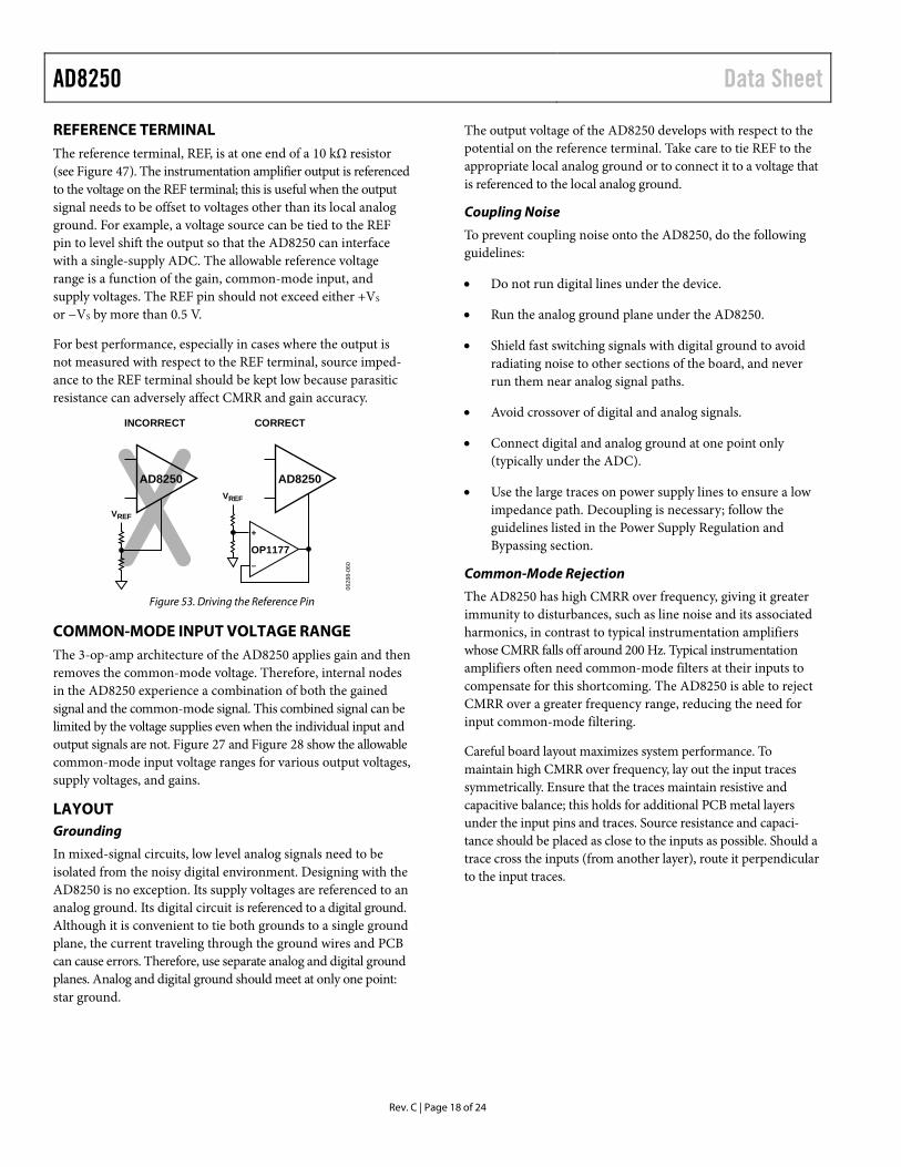
REFERENCE TERMINAL The reference terminal, REF, is at one end of a 10 kΩ resistor (see Figure 47). The instrumentation amplifier output is referenced to the voltage on the REF terminal; this is useful when the output signal needs to be offset to voltages other than its local analog ground. For example, a voltage source can be tied to the REF pin to level shift the output so that the AD8250 can interface with a single-supply ADC. The allowable reference voltage range is a function of the gain, common-mode input, and supply voltages. The REF pin should not exceed either +VS or −VS by more than 0.5 V.
For best performance, especially in cases where the output is not measured with respect to the REF terminal, source imped-ance to the REF terminal should be kept low because parasitic resistance can adversely affect CMRR and gain accuracy.
INCORRECT
AD8250
VREF
CORRECT
AD8250
OP1177+
–
VREF
0628
8-06
0
Figure 53. Driving the Reference Pin
COMMON-MODE INPUT VOLTAGE RANGE The 3-op-amp architecture of the AD8250 applies gain and then removes the common-mode voltage. Therefore, internal nodes in the AD8250 experience a combination of both the gained signal and the common-mode signal. This combined signal can be limited by the voltage supplies even when the individual input and output signals are not. Figure 27 and Figure 28 show the allowable common-mode input voltage ranges for various output voltages, supply voltages, and gains.
LAYOUT Grounding
In mixed-signal circuits, low level analog signals need to be isolated from the noisy digital environment. Designing with the AD8250 is no exception. Its supply voltages are referenced to an analog ground. Its digital circuit is referenced to a digital ground. Although it is convenient to tie both grounds to a single ground plane, the current traveling through the ground wires and PCB can cause errors. Therefore, use separate analog and digital ground planes. Analog and digital ground should meet at only one point: star ground.
The output voltage of the AD8250 develops with respect to the potential on the reference terminal. Take care to tie REF to the appropriate local analog ground or to connect it to a voltage that is referenced to the local analog ground.
Coupling Noise
To prevent coupling noise onto the AD8250, do the following guidelines:
• Do not run digital lines under the device.
• Run the analog ground plane under the AD8250.
• Shield fast switching signals with digital ground to avoid radiating noise to other sections of the board, and never run them near analog signal paths.
• Avoid crossover of digital and analog signals.
• Connect digital and analog ground at one point only (typically under the ADC).
• Use the large traces on power supply lines to ensure a low impedance path. Decoupling is necessary; follow the guidelines listed in the Power Supply Regulation and Bypassing section.
Common-Mode Rejection
The AD8250 has high CMRR over frequency, giving it greater immunity to disturbances, such as line noise and its associated harmonics, in contrast to typical instrumentation amplifiers whose CMRR falls off around 200 Hz. Typical instrumentation amplifiers often need common-mode filters at their inputs to compensate for this shortcoming. The AD8250 is able to reject CMRR over a greater frequency range, reducing the need for input common-mode filtering.
Careful board layout maximizes system performance. To maintain high CMRR over frequency, lay out the input traces symmetrically. Ensure that the traces maintain resistive and capacitive balance; this holds for additional PCB metal layers under the input pins and traces. Source resistance and capaci-tance should be placed as close to the inputs as possible. Should a trace cross the inputs (from another layer), route it perpendicular to the input traces.
Data Sheet AD8250
Rev. C | Page 19 of 24
RF INTERFERENCE RF rectification is often a problem when amplifiers are used in applications where there are strong RF signals. The disturbance can appear as a small dc offset voltage. High frequency signals can be filtered with a low-pass RC network placed at the input of the instrumentation amplifier, as shown in Figure 54. The filter limits the input signal bandwidth according to the following relationship:
)(221
CDDIFF CCR
FilterFreq
CCM RC
FilterFreq2
1
where CD ≥ 10 CC.
R
R
AD8250
+15V
+IN
–IN
0.1µF 10µF
10µF0.1µF
REF
–15V
CD
CC
CC
0628
8-06
1
OUT
Figure 54. RFI Suppression
Values of R and CC should be chosen to minimize RFI. A mismatch between the R × CC at the positive input and the R × CC at the negative input degrades the CMRR of the AD8250. By using a value of CD that is 10 times larger than the value of CC, the effect of the mismatch is reduced and performance is improved.
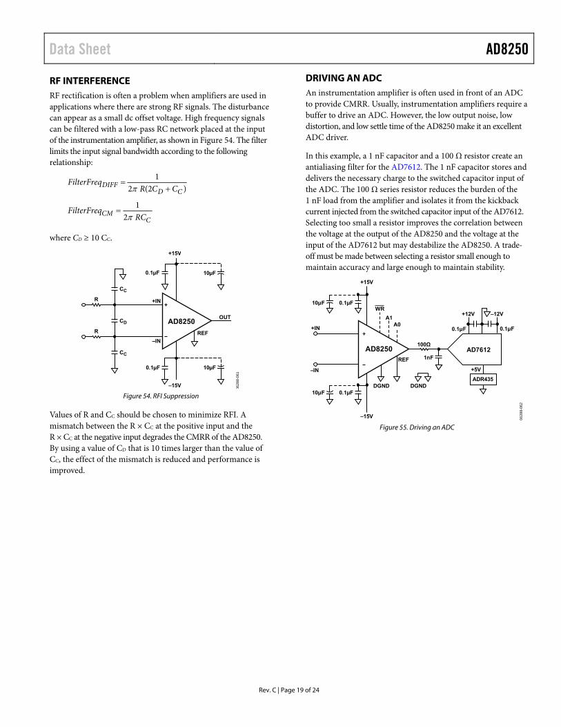
DRIVING AN ADC An instrumentation amplifier is often used in front of an ADC to provide CMRR. Usually, instrumentation amplifiers require a buffer to drive an ADC. However, the low output noise, low distortion, and low settle time of the AD8250 make it an excellent ADC driver.
In this example, a 1 nF capacitor and a 100 Ω resistor create an antialiasing filter for the AD7612. The 1 nF capacitor stores and delivers the necessary charge to the switched capacitor input of the ADC. The 100 Ω series resistor reduces the burden of the 1 nF load from the amplifier and isolates it from the kickback current injected from the switched capacitor input of the AD7612. Selecting too small a resistor improves the correlation between the voltage at the output of the AD8250 and the voltage at the input of the AD7612 but may destabilize the AD8250. A trade-off must be made between selecting a resistor small enough to maintain accuracy and large enough to maintain stability.
0.1μF0.1μF
1nF
100ΩAD7612
ADR435
+12V –12V
+5V
+15V
–15V
A0A1
WR
+IN
–IN
10μF 0.1µF
10μF 0.1µF
REF
AD8250
0628
8-06
2
DGNDDGND
Figure 55. Driving an ADC
AD8250 Data Sheet
Rev. C | Page 20 of 24
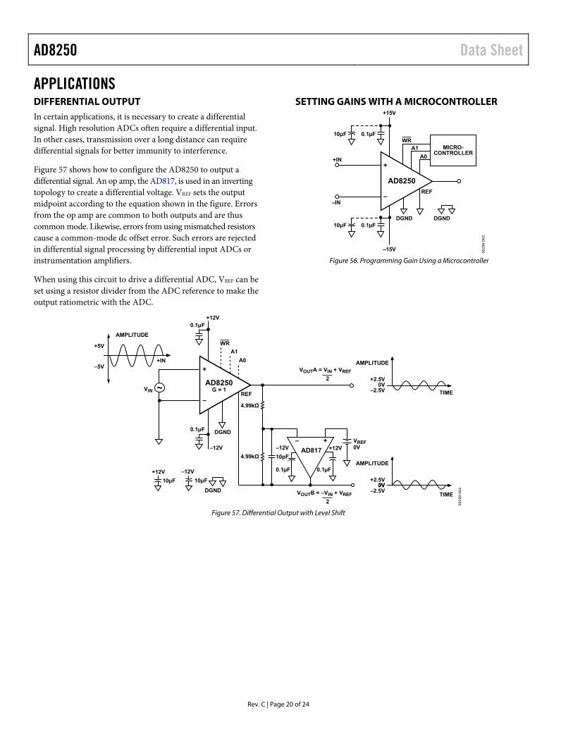
APPLICATIONS DIFFERENTIAL OUTPUT In certain applications, it is necessary to create a differential signal. High resolution ADCs often require a differential input. In other cases, transmission over a long distance can require differential signals for better immunity to interference.
Figure 57 shows how to configure the AD8250 to output a differential signal. An op amp, the AD817, is used in an inverting topology to create a differential voltage. VREF sets the output midpoint according to the equation shown in the figure. Errors from the op amp are common to both outputs and are thus common mode. Likewise, errors from using mismatched resistors cause a common-mode dc offset error. Such errors are rejected in differential signal processing by differential input ADCs or instrumentation amplifiers.
When using this circuit to drive a differential ADC, VREF can be set using a resistor divider from the ADC reference to make the output ratiometric with the ADC.
SETTING GAINS WITH A MICROCONTROLLER +15V
MICRO-CONTROLLER
–15V
A0
A1WR
+IN
–IN
10μF 0.1µF
10μF 0.1µF
REF
AD8250
0628
8-06
3
+
–
DGNDDGND
Figure 56. Programming Gain Using a Microcontroller
+12V
–12V
A0
A1
WR
+IN
10μF
0.1μF
10μF
0.1μF
AD8250
REFG = 1
0.1µF
4.99kΩ
4.99kΩAD817
0.1µF
+12V–12VVREF0V
VOUTA = VIN + VREF
2
2
VOUTB = –VIN + VREF
+2.5V
–2.5V0V
+2.5V
–2.5V0V
TIME
AMPLITUDE
0V
TIME
AMPLITUDE
+5V
–5V
AMPLITUDE
10pF
+12V –12V
VIN
0628
8-06
4
+
–
+–DGND
DGND
Figure 57. Differential Output with Level Shift
Data Sheet AD8250
Rev. C | Page 21 of 24
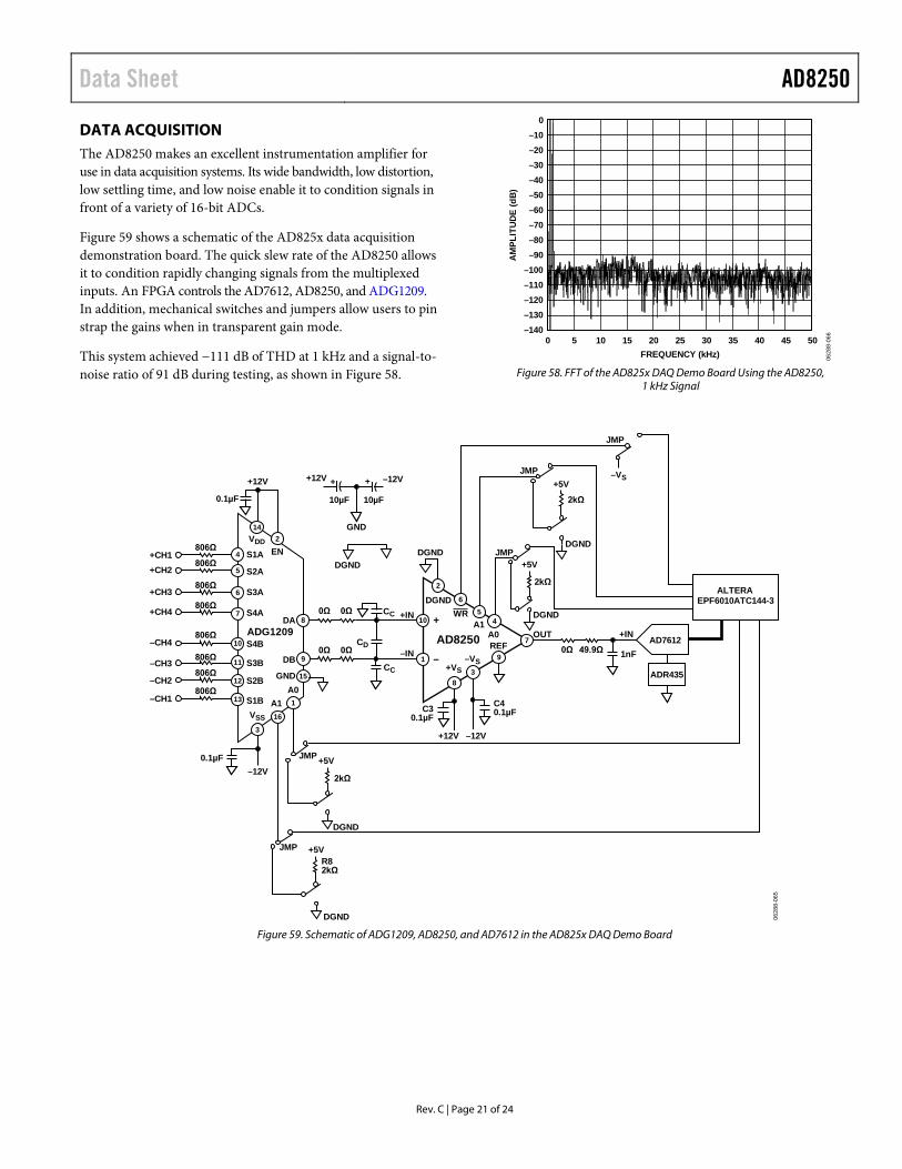
DATA ACQUISITION The AD8250 makes an excellent instrumentation amplifier for use in data acquisition systems. Its wide bandwidth, low distortion, low settling time, and low noise enable it to condition signals in front of a variety of 16-bit ADCs.
Figure 59 shows a schematic of the AD825x data acquisition demonstration board. The quick slew rate of the AD8250 allows it to condition rapidly changing signals from the multiplexed inputs. An FPGA controls the AD7612, AD8250, and ADG1209. In addition, mechanical switches and jumpers allow users to pin strap the gains when in transparent gain mode.
This system achieved −111 dB of THD at 1 kHz and a signal-to-noise ratio of 91 dB during testing, as shown in Figure 58.
0
–140–130–120–110–100
–90–80–70–60–50–40–30–20–10
0 5 10 15 20 25 30 35 40 45 50
AM
PLIT
UD
E (d
B)
FREQUENCY (kHz) 0628
8-06
6
Figure 58. FFT of the AD825x DAQ Demo Board Using the AD8250,
1 kHz Signal
0628
8-06
5
AD8250
2
+IN
–IN
A1A0 OUTREF
–VS+VS
DGND
5
3
4
9
1
7
10
11
12
13
14
15
16
6
2
S1A EN
S2A
S3A
S4A
S1B
S2B
DB
GND
DA
S3B
S4B
A0A1
VSS
VDDJMP
JMP
JMP
+12V –12V
+12V
–12V
JMP
JMP
–VS+5V
+5V
DGND806Ω
806Ω
806Ω
806Ω
806Ω
806Ω
806Ω
806Ω
0Ω
0Ω 49.9Ω0Ω
–CH1
+CH1+CH2
–CH2
+CH3
–CH3
+CH4
–CH41nF
2kΩ
2kΩ
0.1µF
GND
+12V –12V+ +
10µF 10µF0.1µF
CD
CC
CC
C30.1µF
C40.1µF
+5V
+5V
DGND
DGND
R82kΩ
+IN AD7612
ADR435
ADG1209
DGND
ALTERAEPF6010ATC144-3
80Ω
0Ω1
10
6
WR
9
45
83
7
+
–
DGND
2kΩ
DGND
Figure 59. Schematic of ADG1209, AD8250, and AD7612 in the AD825x DAQ Demo Board
AD8250 Data Sheet
Rev. C | Page 22 of 24
OUTLINE DIMENSIONS
COMPLIANT TO JEDEC STANDARDS MO-187-BA 0917
09-A
6°0°
0.700.550.40
5
10
1
6
0.50 BSC
0.300.15
1.10 MAX
3.103.002.90
COPLANARITY0.10
0.230.13
3.103.002.90
5.154.904.65
PIN 1IDENTIFIER
15° MAX0.950.850.75
0.150.05
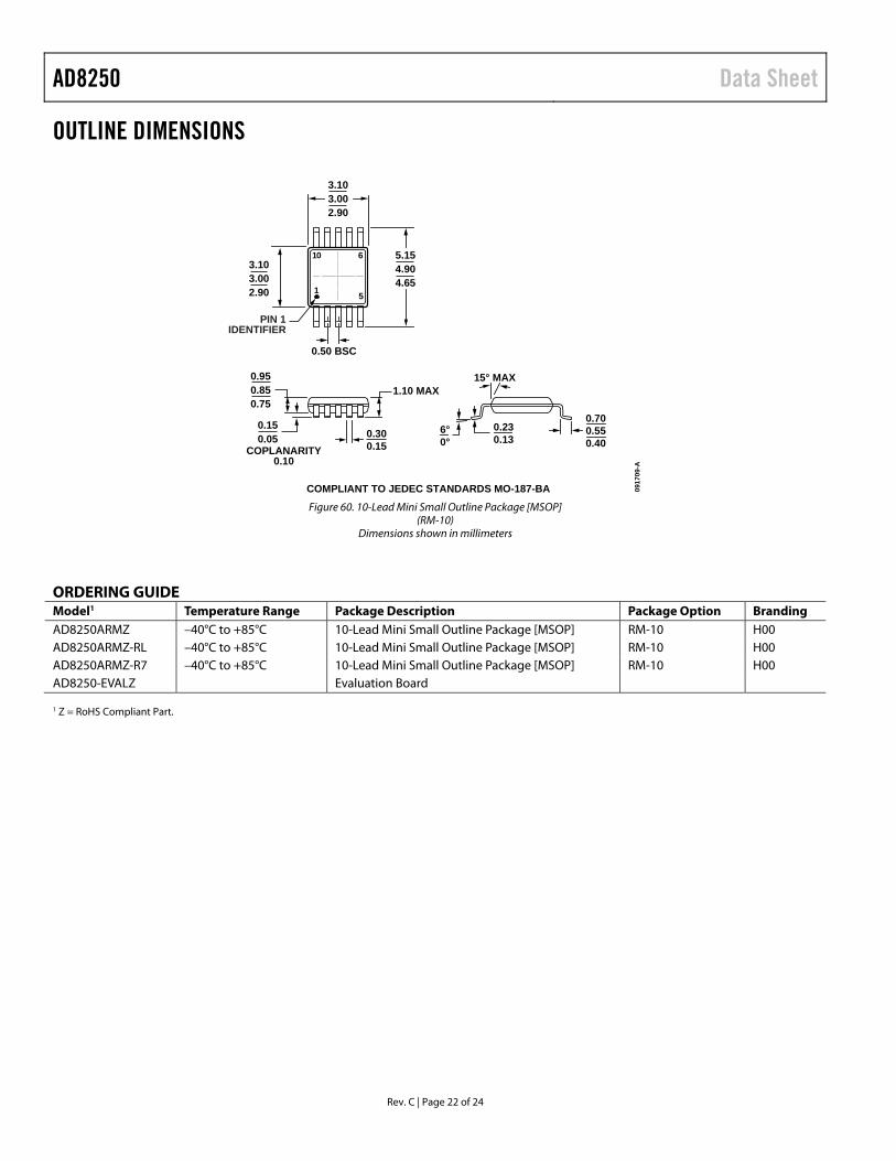
Figure 60. 10-Lead Mini Small Outline Package [MSOP]
(RM-10) Dimensions shown in millimeters
ORDERING GUIDE Model1 Temperature Range Package Description Package Option Branding AD8250ARMZ –40°C to +85°C 10-Lead Mini Small Outline Package [MSOP] RM-10 H00 AD8250ARMZ-RL –40°C to +85°C 10-Lead Mini Small Outline Package [MSOP] RM-10 H00 AD8250ARMZ-R7 –40°C to +85°C 10-Lead Mini Small Outline Package [MSOP] RM-10 H00 AD8250-EVALZ Evaluation Board 1 Z = RoHS Compliant Part.

Data Sheet AD8250
Rev. C | Page 23 of 24
NOTES

AD8250 Data Sheet
Rev. C | Page 24 of 24
NOTES
©2007–2013 Analog Devices, Inc. All rights reserved. Trademarks and registered trademarks are the property of their respective owners. D06288-0-5/13(C)