Embed Size (px)
Citation preview

iW3602AC/DC Digital Power Controller for Dimmable LED Drivers
Rev. 0.94 PreliminaryiW3602
© 2014 Dialog Semiconductor (UK) Ltd.Datasheet 1 of 19
1.0 Features Isolated AC/DC offline 100VAC /230VAC LED driver
Line frequency ranges from 45Hz to 66Hz
Intelligent wall dimmer detection
x Leading-edge dimmer
x Trailing-edge dimmer
x No-dimmer detected
x Unsupported dimmer
Hybrid dimming scheme
Wide dimming range from 1% up to 100%
No visible flicker
Resonant control to achieve high efficiency, 85% without dimmer
Temperature compensated LED current
Small size design
x Small size input bulk capacitor
x Small size output capacitor
x Small transformer
Primary-side sensing eliminates the need for opto-isolator feedback and simplifies design
Tight LED current regulation ± 5%
Fast start-up, typically 10µA start-up current
Hot-plug LED module support
Multiple protection features:
x LED open circuit protection
x Single-fault protection
x Over-current protection
x LED short circuit protection
x Current sense resistor short circuit protection
x Over-temperature protection
x Input over-voltage protection
Up to 10W output power
2.0 DescriptionThe iW3602 is a high performance AC/DC offline power supply controller for dimmable LED luminaires, which uses advanced digital control technology to detect the dimmer type and phase. The dimmer conduction phase controls the LED brightness. The LED brightness is modulated by PWM-dimming. The iW3602’s unique digital control technology eliminates visible flicker.
The iW3602 can operate with all dimmer schemes including: leading-edge dimmer, trailing-edge dimmer, as well as other dimmer configurations such as R-type, R-C type or R-L type. When a dimmer is not present, the controller can automatically detect that there is no dimmer.
The iW3602 operates in a quasi-resonant mode to provide high efficiency. The iW3602 provides a number of key built-in features. The iW3602 uses advanced primary-side sensing technology to achieve excellent line and load regulation without secondary feedback circuitry. In addition, the iW3602’s pulse-by-pulse waveform analysis technology allows accurate LED current regulation. The iW3602 maintains stability over all operating conditions without the need for loop compensation components. Therefore, the iW3602 minimizes external component count, simplifies EMI design and lowers overall bill of materials cost.
3.0 Applications Dimmable LED luminaires
Optimized for 3W to 10W output power

iW3602AC/DC Digital Power Controller for Dimmable LED Drivers
Rev. 0.94 PreliminaryiW3602
© 2014 Dialog Semiconductor (UK) Ltd.Datasheet 2 of 19
Pin # Name Type Pin Description1 OUTPUT(TR) Output Gate drive for chopping MOSFET switch.
2 VSENSE Analog Input Auxiliary voltage sense (used for primary side regulation and ZVS).
3 VIN Analog Input Rectified AC line voltage sense.
4 VT Analog Input External power limit and shutdown control.
5 GND Ground Ground.
6 ISENSE Analog Input Primary current sense (used for cycle-by-cycle peak current control and limit).
7 OUTPUT Output Gate drive for main MOSFET switch.
8 VCC Power Input Power supply for control logic and voltage sense for power-on reset circuitry.
Figure 3.1 : iW3602 Typical Application Circuit
AC InputFrom Dimmer VOUT
RTN
+
U1iW3602
NTCThermistor
OUTPUT(TR)
VSENSE
VIN
VT
VCC
OUTPUT
ISENSE
GND
1
2
3
8
7
6
4 5
+
ChoppingCircuit
Isolated FlybackConverter
+
4.0 Pinout DescriptioniW3602
1
2
3
8
7
6
4 5
VCC
VSENSE
VIN
VT
ISENSE
GND
OUTPUT(TR)
OUTPUT
Figure 4.1 : 8 Lead SOIC-8 Package

iW3602AC/DC Digital Power Controller for Dimmable LED Drivers
Rev. 0.94 PreliminaryiW3602
© 2014 Dialog Semiconductor (UK) Ltd.Datasheet 3 of 19
Absolute maximum ratings are the parameter values or ranges which can cause permanent damage if exceeded. For maximum safe operating conditions, refer to Electrical Characteristics in Section 6.0.
5.0 Absolute Maximum Ratings
Parameter Symbol Value UnitsDC supply voltage range (pin 8, ICC = 20mA max) VCC -0.3 to 18 V
DC supply current at VCC pin ICC 20 mA
OUTPUT (pin 7) -0.3 to 18 V
OUTPUT(TR) (pin 1) -0.3 to 18 V
VSENSE input (pin 2, IVsense ≤ 10mA) -0.7 to 4.0 V
VIN input (pin 3) -0.3 to 18 V
ISENSE input (pin 6) -0.3 to 4.0 V
VT input (pin 4) -0.3 to 4.0 V
Power dissipation at TA ≤ 25°C PD 526 mW
Maximum junction temperature TJMAX 150 °C
Operating junction temperature TJOPT -40 to 150 °C
Storage temperature TSTG -65 to 150 °C
Thermal Resistance
Junction-to-PCB Board Surface Temperature ψJB (Note 1) 70
°C/WJunction-to-Ambient [Still Air] θJA 160
ESD rating per JEDEC JESD22-A114 ±2,000 V
Latch-up test per JESD78A ±100 mA
Notes:
Note 1. ψJB [Psi Junction to Board] provides an estimation of the die junction temperature relative to the PCB [Board] surface temperature. This data is measured at the ground pin (pin 5) without using any thermal adhesives. For iW3602-01 and iW3602-03 (with exposed pad), ψJB = 70°C/W. See Section 9.13 for more information.

iW3602AC/DC Digital Power Controller for Dimmable LED Drivers
Rev. 0.94 PreliminaryiW3602
© 2014 Dialog Semiconductor (UK) Ltd.Datasheet 4 of 19
Parameter Symbol Test Conditions Min Typ Max UnitVIN SECTION (Pin 3)
Start-up current IINST VIN = 10V, CVCC = 10µF 10 15 µA
Input impedance ZIN TA = 25°C 2.5 kW
VIN Range VIN 0 1.8 V
VSENSE SECTION (Pin 2)
Input leakage current IIN(Vsense) VSENSE = 2V 1 μA
Nominal voltage threshold VSENSE(NOM) TA = 25°C, negative edge 1.523 1.538 1.553 V
Output OVP threshold VSENSE(MAX) TA = 25°C, negative edge 1.65 1.7 1.75 V
OUTPUT SECTION (Pin 7)
Output low level ON-resistance RDS(ON)LO ISINK = 5mA 30 W
Output high level ON-resistance RDS(ON)HI ISOURCE = 5mA 150 W
Rise time (Note 2) tRTA = 25°C, CL = 330pF 10% to 90% 150 ns
Fall time (Note 2) tFTA = 25°C, CL = 330 pF 90% to 10 30 ns
Maximum switching frequency (Note 3) fSW(MAX) 200 kHz
VCC SECTION (Pin 8)
Maximum operating voltage VCC(MAX) 16 V
Start-up threshold VCC(ST) VCC rising 11 12 13 V
Undervoltage lockout threshold VCC(UVL) VCC falling 7 7.5 8 V
Operating current ICCQ CL = 330pF, VSENSE = 1.5V 4.1 4.7 mA
Zener diode clamp voltage VZ(CLAMP) TA = 25°C, IZ = 5mA 18.5 19 20.5 V
ISENSE SECTION (Pin 6)
Over-current limit threshold VOCP 1.83 1.89 1.95 V
ISENSE short protection reference VRSNS 0.16 V
CC regulation threshold limit (Note 4) VREG-TH 1.8 V
VT SECTION (Pin 4)
Power limit high threshold (Note 4) VP-LIM(HI) 0.56 V
Power limit low threshold (Note 4) VP-LIM(LO) 0.44 V
VCC = 12V, -40°C ≤ TA ≤ 85°C, unless otherwise specified (Note 1)6.0 Electrical Characteristics

iW3602AC/DC Digital Power Controller for Dimmable LED Drivers
Rev. 0.94 PreliminaryiW3602
© 2014 Dialog Semiconductor (UK) Ltd.Datasheet 5 of 19
6.0 Electrical Characteristics (cont.)VCC = 12V, -40°C ≤ TA ≤ 85°C, unless otherwise specified (Note 1)
Parameter Symbol Test Conditions Min Typ Max UnitShutdown threshold (Note 4) VSH-TH 0.22 V
Input leakage current IIN(VT) VT = 1.0V 1 µA
Pull-up current source IVT 90 100 110 µA
OUTPUT(TR) SECTION (Pin 1)
Output low level ON-resistance RDS-TR(ON)LO ISINK = 5mA 100 Ω
Output high level ON-resistance RDS-TR(ON)HI ISOURCE = 5mA 200 Ω
Notes:Note 1. Adjust VCC above the start-up threshold before setting at 12V.Note 2. These parameters are not 100% tested. They are guaranteed by design and characterization.Note 3. Operating frequency varies based on the line and load conditions, see Theory of Operation for more details.Note 4. These parameters refer to digital preset values, and they are not 100% tested.

iW3602AC/DC Digital Power Controller for Dimmable LED Drivers
Rev. 0.94 PreliminaryiW3602
© 2014 Dialog Semiconductor (UK) Ltd.Datasheet 6 of 19
7.0 Typical Performance Characteristics
0.00.0
6.0
3.0
9.0
2.0 6.0 10.0 14.0VCC (V)
VC
C S
uppl
y St
art-u
p C
urre
nt (µ
A)
4.0 8.0 12.0
Figure 7.1 : VCC vs. VCC Supply Start-up Current
-50
12.0
-25 25 75 125Ambient Temperature (°C)
VC
C S
tart
-up
Thre
shol
d (V
)
0 50 100
12.2
11.8
11.6
Figure 7.2 : Start-Up Threshold vs. Temperature
-50 -25 25 75 125
Ambient Temperature (°C)% D
evia
tion
of S
witc
hing
Fre
quen
cy fr
om Id
eal
0 50 100
0.3 %
-0.3 %
-0.9 %
-1.5 %
Figure 7.3 : % Deviation of Switching Frequency to Ideal Switching Frequency vs. Temperature
1.98-50
2.00
1.99
2.01
-25 25 75 125Ambient Temperature (°C)
Inte
rnal
Ref
eren
ce V
olta
ge (V
)
0 50 100
Figure 7.4 : Internal Reference vs. Temperature

iW3602AC/DC Digital Power Controller for Dimmable LED Drivers
Rev. 0.94 PreliminaryiW3602
© 2014 Dialog Semiconductor (UK) Ltd.Datasheet 7 of 19
8.0 Functional Block DiagramThe iW3602 combines two functions: 1) wall dimmer type detection and dimmer phase measurement; and 2) output LED light dimming. It uses digital control technology, which consists of: 1) chopping circuit, which helps to increase the power factor and serves as a dynamic impedance to load the dimmer; 2) primary side controlled isolated flyback converter. The iW3602 provides a low cost dimming solution which enables LED bulb to be used with most of the common wall dimmers. This allows LED bulbs to directly replace conventional incandescent bulbs with ease. The iW3602 can detect and operate with leading-edge, and trailing-edge dimmers as well as no-dimmer. The controller operates in critical discontinuous conduction mode (CDCM) to achieve high power efficiency and minimum EMI. It incorporates proprietary primary-feedback constant current control technology to achieve tight LED current regulation.
Figure 3.1 shows a typical iW3602 application schematic. Figure 8.1 shows the functional block diagram. The advanced digital control mechanism reduces system design time and improves reliability. The start-up algorithm makes sure the VCC supply voltage is ready before powering up the IC.
The iW3602 provides multiple protection features for current limit, over-voltage protection, and over temperature protection. The VT function can provide over-temperature compensation for the LED. The external NTC senses the LED temperature. If the VT pin voltage is below VP-LIM(HI), the controller reduces the LED current. If the VT pin voltage is below VSH-TH then the controller turns off.
Figure 8.1 : iW3602 Functional Block Diagram
–
+
VIN
GND
Enable
VCC
5
VT 4
VSENSEVFB
VVMS
VIPK
OUTPUT
ISENSE6
1.89V
0V ~ 1.8V
VIN_A0.0V ~ 1.8V
IPEAK
VOCP
Start-up
DAC
–
+
2
3 8
GateDriver
Enable
ZIN
100µA
65kΩ
7
DimmerDetection
andDimmer PhaseMeasurement
ADCMUX ADC
GateDriver
OUTPUT(TR)
65kΩ
1
VOVP
SignalConditioning
ConstantCurrentControl

iW3602AC/DC Digital Power Controller for Dimmable LED Drivers
Rev. 0.94 PreliminaryiW3602
© 2014 Dialog Semiconductor (UK) Ltd.Datasheet 8 of 19
Pin 6 – ISENSE
Primary current sense. Used for cycle-by-cycle peak current control.
Pin 7 – OUTPUT
Gate drive for the external MOSFET switch.
Pin 8 – VCC
Power supply for the controller during normal operation. The controller starts up when VCC reaches 12V (typical) and shuts down when the VCC voltage is below 7.5V (typical).
High-frequency transients and ripples can be easily generated on the VCC pin due to power supply switching transitions and line and load disturbances. Excess ripples and noises on VCC may cause the iW3602 to function undesirably, hence a decoupling capacitor must be connected between the VCC pin and GND. It is suggested that a ceramic capacitor of minimum 0.1uF be connected as close as possible to the VCC pin.
9.2 Wall Dimmer DetectionsThere are two types of wall dimmers: leading-edge dimmer and trailing-edge dimmer.
AC line before Wall-
dimmer
AC line after Wall-dimmer
Figure 9.1 : Leading-Edge Wall Dimmer Waveforms
9.0 Theory of OperationThe iW3602 is a high performance AC/DC off-line power supply controller for dimmable LED luminaires, which uses advanced digital control technology to detect the dimmer type and dimmer phase to control the LED brightness. A PWM-dimming scheme is used to modulate the LED current with a dimming frequency of 900Hz at low dimming levels. The iW3602 can work with all types of wall dimmers including leading-edge dimmer, trailing-edge dimmer, as well as dimmer configurations such as R-type, R-C type or R-L type without visible flicker. The controller can also work when no dimmer is connected.
The iW3602 operates in quasi-resonant mode to provide high efficiency and simplify EMI design. In addition, the iW3602 includes a number of key built-in protection features. Using the state-of-the-art primary-feedback technology, the iW3602 removes the need for secondary feedback circuitry while achieving excellent line and load regulation. The iW3602 also eliminates the need for loop compensation components while maintaining stability over all operating conditions. Pulse-by-pulse waveform analysis allows for accurate LED current regulation. Hence, the iW3602 can provide high performance dimming solutions, with minimal external component count and low bill of materials cost.
9.1 Pin DetailPin 1 – OUTPUT(TR)
Gate drive for the chopping circuit MOSFET switch.
Pin 2 – VSENSE
Sense signal input from auxiliary winding. This pin provides secondary voltage feedback used for output regulation.
Pin 3 – VIN
Sense signal input from the rectified line voltage. VIN is used for dimmer phase detection. The input line voltage is scaled down using a resistor network. It is used for input under-voltage and over-voltage protection. This pin also provides the supply current to the IC during start-up.
Pin 4 – VT
External power limit and shutdown control. If the shutdown control is not used, this pin should be connected to GND via a resistor.
Pin 5 – GND
Ground.

iW3602AC/DC Digital Power Controller for Dimmable LED Drivers
Rev. 0.94 PreliminaryiW3602
© 2014 Dialog Semiconductor (UK) Ltd.Datasheet 9 of 19
AC line after Wall-dimmer
AC line before Wall-dimmer
Figure 9.2 : Trailing-Edge Wall Dimmer Waveforms
Dimmer detection, or discovery, takes place during the third cycle after start-up. The controller determines whether no dimmer exists, or if there is a leading-edge dimmer or a trailing-edge dimmer.
The VCROSS is internally generated by comparing the digitalized VIN signal to the threshold of 0.25V during dimming and 0.14V without a dimmer. The VIN period (tPERIOD) is measured between two consecutive rising edge zero-crossings. The tCROSS is generated by the internal digital block (refer to Figure 9.3); when VIN_A is higher than 0.14V, tCROSS is set to high and when VIN_A falls below 0.14V tCROSS is reset to zero. If tCROSS is much shorter than the VIN period then a dimmer is detected. The controller uses the filtered derivatives to decide which type of dimmer is present. A large positive derivative value indicates a leading-edge dimmer. Then the controller enters leading-edge dimmer mode; otherwise it enters trailing-edge dimmer mode.
During the dimmer detection stage, the OUTPUT(TR) keeps high to turn on the switch FET in the chopping circuit. This creates a resistive load for the wall dimmer.
0.14 V
OUTPUT(TR)
LED(EN)
VLED
VCROSS
VIN_A
tCROSS
tperiod
Figure 9.3 : Dimmer Detection
9.3 Dimmer Tracking and Phase Measurements
The dimmer detection algorithm and the dimmer tracking algorithm both depend on an accurate input voltage period
measurement. The VIN period is measured during the second cycle of the dimmer detection process and is latched for use thereafter. Using the measured VIN period in subsequent calculations rather than a constant allows for automatic 50/60Hz operation and allows for a 10% frequency variation.
The phase measurement starts when VIN exceeds the rising threshold until VIN falls below the falling threshold.
VCROSS
tPERIOD
tCROSS
t0
0.14 V
Figure 9.4 : Dimmer Phase Measurement
The dimmer phase is calculated as:
Dimmer Phase CROSS
PERIOD
tt
= (9.1)
The calculated dimmer phase is used to generate the signal DRATIO, which determines LED current. If the dimmer phase is less than 0.14 then the DRATIO is clamped at 0.14; if the dimmer phase is greater than 0.7 then DRATIO is clamped at 1.0; otherwise DRATIO is calculated by equation 9.2.
1 2Dimmer PhaseRATIOD K K= × − (9.2)
Where, K1 is set to 1.768 and K2 is set to 0.238.
Using VIsense(NOM) to represent the nominal 100% LED current, the VIsense, which modulates the output LED current, is controlled by:
( )Isense Isense NOM RATIOV V D= × (9.3)
When DRATIO is 1, the converter outputs 100% of nominal power to the LED. If DRATIO is 0.01, the converter outputs 1% of nominal power to the LED.

iW3602AC/DC Digital Power Controller for Dimmable LED Drivers
Rev. 0.94 PreliminaryiW3602
© 2014 Dialog Semiconductor (UK) Ltd.Datasheet 10 of 19
9.4 Chopping Operation
AC
WallDimmer
+
BR
OUTPUT(TR)
VIN_A
*R2
RC
LC
R1
D1
D2VCB
QCCB
*R2 is internal ZIN of IC
RS
Figure 9.5 : Chopping Schematic
Chopping circuit provides the dynamic impedance for the dimmer and builds the energy to the LED power converter. It consists of LC, QC, RC, RS, and D2. LC is the chopping inductor. During the chopping period, LC is used to store the energy when the QC is on, and then release the energy to CB when QC is off. The on-time of QC during the chopping period when no dimmer exists is calculated by the following equation:
( ) _4 2.2 sVON Qc IN AT s Vµ= µ − × (9.4)
For the IW3602-03 part, the on-time of QC doubles the on-time specified by equation 9.4. If a dimmer exists then the on-time of QC is determined by equation 9.4. The period of QC is calculated by:
( ) _12.2 8.8 sVPERIOD Qc IN AT s Vµ= µ + × (9.5)
VIN_A is the scale voltage of VIN. VCB is the voltage across CB. When tCROSS is low, QC is always on. When tCROSS is high, QC operates according to equation 9.4 and 9.5.
During the chopping period, the average current of LC is in phase with the input AC line voltage, so it inherently generates a high power factor. D1 in the chopping circuit is used to charge CB when the voltage of CB is lower than the input line voltage. This helps to reduce the inrush current when the TRIAC is fired.
3
2
4
1Time (2.0 ms/div)
VIN pin signal500 mV/div
OUTPUT(TR)10.0 V/div
ILC100 mA/div
tCROSS5.0 V/div
3
2
4
1Time (2.0 ms/div)
VIN pin signal500 mV/div
OUTPUT(TR)10.0 V/div
ILC100 mA/div
tCROSS5.0 V/div
Figure 9.6 : Signals of Chopping Circuit.
9.5 Start-upPrior to start-up the VIN pin charges up the VCC capacitor through a diode between VIN and VCC. When VCC is fully charged to a voltage higher than the start-up threshold VCC(ST), the ENABLE signal becomes active and enables the control logic, shown by Figure 9.7. When the control logic is enabled, the controller enters normal operation mode. During the first 3 half AC cycles, OUTPUT(TR) keeps high. After the dimmer type and AC line period are measured, the constant current stage is enabled and the output voltage starts to ramp up. When the output voltage is above the forward voltage of the LED, the controller begins to operate in constant current mode.
An adaptive soft-start control algorithm is applied during the start-up state, where the initial output pulses are short and gradually get wider until the full pulse width is achieved. The peak current is limited cycle by cycle by the IPEAK comparator.

iW3602AC/DC Digital Power Controller for Dimmable LED Drivers
Rev. 0.94 PreliminaryiW3602
© 2014 Dialog Semiconductor (UK) Ltd.Datasheet 11 of 19
VCC
VCC(ST)
ENABLE
Start-up Sequencing
VIN
Figure 9.7 : Start-up Sequencing Diagram
9.6 Understanding Primary FeedbackFigure 9.8 illustrates a simplified flyback converter. When the switch Q1 conducts during tON(t), the current ig(t) is directly drawn from rectified vg(t). The energy Eg(t) is stored in the magnetizing inductance LM. The rectifying diode D1 is reversely biased and the load current IO is supplied by the secondary capacitor CO. When Q1 turns off, D1 conducts and the stored energy Eg(t) is delivered to the output.
+
vin(t)
TS(t)
IO
VO
VAUX
N:1
D1
Q1
VAUX
CO vg(t)
ig(t) +
–
iin(t) id(t)
Figure 9.8 : Simplified Flyback Converter
In order to tightly regulate the output voltage, the information about the output voltage and load current must be accurately sensed. In the DCM flyback converter, this information can be read via the auxiliary winding or the primary magnetizing inductance (LM). During the Q1 on-time, the load current is supplied from the output filter capacitor CO. The voltage across LM is vg(t), assuming the voltage dropped across Q1 is zero. The current in Q1 ramps up linearly at a rate of:
( ) ( )g g
M
di t v tdt L
=
(9.6)
At the end of on-time, the current ramps up to:
_( )
( ) g ONg peak
M
v t ti t
L×
=
(9.7)
This current represents a stored energy of:
2_ ( )
2M
g g peakLE i t= ×
(9.8)
When Q1 turns off, ig(t) in LM forces a reversal of polarities on all windings. Ignoring the communication-time caused by the leakage inductance LK at the instant of turn-off, the primary current transfers to the secondary at a peak amplitude of:
_( ) ( )Pd g peak
S
Ni t i tN
= × (9.9)
Assuming the secondary winding is master and the auxiliary winding is slave.
VAUX
0V
VAUX = -VIN x NAUX
NP
VAUX = VO x NAUX
NS
Figure 9.9 : Auxiliary Voltage Waveforms
The auxiliary voltage is given by:
( )AUXAUX O
S
NV V V
N= + ∆
(9.10)
and reflects the output voltage as shown in Figure 9.9.
The voltage at the load differs from the secondary voltage by a diode drop and IR losses. The diode drop is a function of current, as are IR losses. Thus, if the secondary voltage is always read at a constant secondary current, the difference between the output voltage and the secondary voltage is a fixed ΔV. If the voltage can be read when the secondary current is small, for example, at the knee of the auxiliary waveform (see Figure 9.9), then ΔV is also small. With the iW3602, ΔV can be ignored.
The real-time waveform analyzer in the iW3602 reads the auxiliary waveform information cycle by cycle. The part then generates a feedback voltage VFB. The VFB signal precisely

iW3602AC/DC Digital Power Controller for Dimmable LED Drivers
Rev. 0.94 PreliminaryiW3602
© 2014 Dialog Semiconductor (UK) Ltd.Datasheet 12 of 19
represents the output voltage and is used to regulate the output voltage.
9.7 Valley Mode SwitchingIn order to reduce switching losses in the MOSFET and EMI, the iW3602 employs valley mode switching during constant output current operation. In valley mode switching, the MOSFET switch is turned on at the point where the resonant voltage across the drain and source of the MOSFET is at its lowest point (see Figure 9.10). By switching at the lowest VDS, the switching loss is minimized.
Gate
VDS
Figure 9.10 : Valley Mode Switching
Turning on at the lowest VDS generates the lowest dV/dt, thus valley mode switching can also reduce EMI. To limit the switching frequency range, the iW3602 can skip valleys (seen the first cycle in Figure 9.10) when the switching frequency is greater than fSW(MAX).
At each of the switching cycles, the falling edge of VSENSE is checked. If the falling edge of VSENSE is not detected, the off-time is extended until the falling edge of VSENSE is detected.
9.8 LED Current RegulationThe iW3602 incorporates a patented primary-side only constant current regulation technology. The iW3602 regulates the output current at a constant level regardless of the output voltage, while avoiding a continuous conduction mode. To achieve this regulation the iW3602 senses the load current indirectly through the primary current. The primary current is detected by the ISENSE pin through a resistor from the MOSFET source to ground.
IP
IS
IO
tON tOFF
tR
tS
Figure 9.11 : Constant LED Current Regulation
The ISENSE resistor determines the maximum current output of the power supply. The output current of the power supply is determined by:
12
REG TH ROUT PS
SENSE S
V tI NR t
−= × × × (9.11)
where NPS is the turns ratio of the primary and secondary windings and RSENSE is the ISENSE resistor.
9.9 VIN ResistorsVIN resistors are chosen primarily to scale down the input voltage for the IC. The scale factor for the input voltage in the IC is 0.0043 for high line, and 0.0086 for low line; if the internal impedance of this pin is selected to be 2.5kΩ. Then for high line, the VIN resistors should equate to:
2.5 2.5 5790.0043Vin
kR k kW= − W = W
(9.12)
9.10 Voltage Protection FunctionsThe iW3602 includes a function that protects against an input over-voltage (VIN OVP) and output over-voltage (OVP).
The input voltage is monitored by VIN_A, as shown in Figure 8.1. If this voltage exceeds 1.8 V for 15 continuous half AC cycles the iW3602 considers VIN to be over-voltage. Output voltage is monitored by the VSENSE pin. If the voltage at this pin exceeds VSENSE(MAX) for two continuous switching cycles the iW3602 considers the output voltage to be over-voltage.
In both input over-voltage and output over-voltage cases, the IC remains biased, which discharges the VCC supply. In order to prevent overcharging the output voltage or overcharging the bulk voltage, the iW3602 employs an extended discharge time before restart. Initially if VCC drops

iW3602AC/DC Digital Power Controller for Dimmable LED Drivers
Rev. 0.94 PreliminaryiW3602
© 2014 Dialog Semiconductor (UK) Ltd.Datasheet 13 of 19
below the UVLO threshold, the controller resets itself and then initiates a new soft-start cycle.
Under a fault condition, the controller tries to start-up for three consecutive times. If all three start-up attempts fail, the controller enters an inactive mode, during which the controller does not respond to VCC power-on requests. The controller is activated again after it sees 29 start-up attempts. The controller can also be reset to the initial condition if VCC is discharged. Typically, this extended discharge time is around 3 to 5 seconds.
This extended discharge time allows the iW3602 to support hot-plug LED modules without causing dangerously high output voltages while maintaining a quick recovery.
9.11 PCL, OC and SRS ProtectionPeak-current limit (PCL), over-current protection (OCP) and sense-resistor short protection (SRSP) are features built-into the iW3602. With the ISENSE pin the iW3602 is able to monitor the primary peak current. This allows for cycle by cycle peak current control and limit. When the primary peak current multiplied by the ISENSE sense resistor is greater than VOCP over-current protection is engaged and the IC immediately turns off the gate drive until the next cycle. The output driver continues to send out switching pulses; the IC immediately turns off the gate drive if the OCP threshold is reached again.
If the ISENSE sense resistor is shorted there is a potential danger of the over-current condition not being detected. Thus the IC is designed to detect this sense-resistor-short fault after the start-up, and shut down immediately. The VCC is discharged since the IC remains biased. In order to prevent overcharging the output voltage, the iW3602 employs an extended discharge time before restart, similar to the discharge time described in section 9.10.
9.12 Over-Temperature ProtectionIf an NTC thermistor is connected from the VT pin to GND then, the iW3602 is able to detect and protect against an over temperature event (OTP).
The iW3602 provides a current (IVT) to the VT pin and detects the voltage on the pin. Based on this voltage the iW3602 can monitor the temperature on the NTC thermistor. As the VT pin voltage reduces, the iW3602 reduces the amount of chopping and the output current according to Figure 9.12. There is a hysteresis of 84mV on VT pin voltage for each power limiting step.
VT Pin Voltage
Perc
enta
ge o
f Nom
inal
Out
put C
urre
nt (%
)
0.0 0.2 0.4 0.6 0.8 1.00
20
40
60
80
100
V P-LIM(H
I)
V P-LIM(LO
)
V SH-TH
VT Pin Voltage
Perc
enta
ge o
f Nom
inal
Out
put C
urre
nt (%
)
0.0 0.2 0.4 0.6 0.8 1.00
20
40
60
80
100
V P-LIM(H
I)
V P-LIM(LO
)
V SH-TH
a) VT from 1.0 V to 0.0 V
b) VT from 0.0 V to 1.0 V
Figure 9.12 : VT Pin Voltage vs. % of Nominal Output Current VT from 1.0V to 0.0V
VT Pin Voltage
Perc
enta
ge o
f Nom
inal
Out
put C
urre
nt (%
)
0.0 0.2 0.4 0.6 0.8 1.00
20
40
60
80
100
V P-LIM(H
I)
V P-LIM(LO
)
V SH-TH
Figure 9.13 : VT Pin Voltage vs. % of Nominal Output Current VT from 0.0V to 1.0V
When the VT pin voltage reaches VP-LIM(HI) the output current begins to reduce as shown in Figure 9.12. At VP-LIM(LO) the output current reduces to 1%. The device can be placed in shutdown mode by pulling the VT pin to ground or below VSH-TH.
9.13 Thermal DesignNote: This section only applies to iW3602-01 and -03.
The iW3602 is typically installed inside a small enclosure, where space and air volumes are constrained. Under these circumstances θJA (thermal resistance, junction to ambient) measurements do not provide useful information for this type of application. Instead we have provided ψJB which estimates the increase in die junction temperature relative to the PCB surface temperature. Figure 9.14 shows the PCB surface temperature is measured at the IC’s GND pin pad.

iW3602AC/DC Digital Power Controller for Dimmable LED Drivers
Rev. 0.94 PreliminaryiW3602
© 2014 Dialog Semiconductor (UK) Ltd.Datasheet 14 of 19
GND pin
Thermal ViasConnect top thermal pad
to bottom copper
Thermal EpoxyArtic Silver
IC Die
Printed Circuit Board
ExposedDie Pad
Copper Thermal Pad Under Package
Printed Circuit Board
JB
ψJB
PCB Top Copper Trace
PCB Bottom Copper Trace
Figure 9.14 : Ways to Improve Thermal Resistance
Using ψJB the junction temperature (TJ) of the IC can be found using the equation below.
JBJ B HT T P= + ⋅ψ (9.13)
where, TB is the PCB surface temperature and PH is the power applied to the chip or the product of VCC and ICCQ.
The iW3602 uses an exposed pad package to reduce the thermal resistance of the package. Although just by using an exposed package can provide some thermal resistance improvement, more significant improvements can be obtained with simple PCB layout and design. Figure 9.13 demonstrates some recommended techniques to improve thermal resistance, which are also highlighted below.
Ways to Improve Thermal Resistance Increase PCB area and associated amount of copper
interconnect.
Use thermal adhesive to attach the package to a thermal pad on PCB.
Connect PCB thermal pad to additional copper on PCB using thermal vias.
Environment ψJB
No adhesive 70 °C/WUse thermal adhesive to pad 63 °C/W
Use thermal adhesive to pad with thermal vias 49 °C/W
Table 9.1: Improvements in ψJB Based on Limited Experimentation
5 15 25
PCB Area (cm2)
ΨJB
(˚C
/Wat
t)
10 20 30
85
65
45
35
75
55
25
~ 30%
Effect of Thermal Resistance Improvements
A: without thermal adhesive and thermal viasB: with thermal adhesive and thermal vias
A
B
Figure 9.15 : Effect of Thermal Resistance Improvements
Figure 9.15 shows improvement of approximately 30% in thermal resistance across different PCB sizes when the exposed pad is attached to PCB using a thermal adhesive and thermal vias connect the pad to a larger plate on the opposing side of the PCB.

iW3602AC/DC Digital Power Controller for Dimmable LED Drivers
Rev. 0.94 PreliminaryiW3602
© 2014 Dialog Semiconductor (UK) Ltd.Datasheet 15 of 19
10.0 Performance Characteristics
Trailing Edge Dimmer
Ch1 500mACh3 200V Ch4 1.0V
3
1
4
Time (2.0 ms/div)
VIN pin signal1.0 V/div
AC linecurrent
500 mA/div
AC line200 V/div
Figure 10.1 : Trailing Edge Dimmer
Trailing Edge Dimmer
Ch1 500mACh3 200V Ch4 1.0V
3
1
4
Time (2.0 ms/div)
VIN pin signal1.0 V/div
AC linecurrent
500 mA/div
AC line200 V/div
Figure 10.2 : Trailing Edge Dimmer 2
Leading Edge Dimmer
Ch1 500mACh3 200V Ch4 1.0V
3
1
4
Time (2.0 ms/div)
VIN pin signal1.0 V/div
AC linecurrent
500 mA/div
AC line200 V/div
Figure 10.3 : Leading Edge Dimmer
Leading Edge Dimmer
Ch1 500mACh3 200V Ch4 1.0V
3
1
4
Time (2.0 ms/div)
VIN pin signal1.0 V/div
AC linecurrent
500 mA/div
AC line200 V/div
Figure 10.4 : Leading Edge Dimmer 2
No Dimmer
Ch1 100mACh3 1.0V Ch4 200V
3
1
4
Time (2.0 ms/div)
VIN pin signal1.0 V/div
AC linecurrent
100 mA/div
AC line200 V/div
Figure 10.5 : No Dimmer
iW3602AC/DC Digital Power Controller for Dimmable LED Drivers
Rev. 0.94 PreliminaryiW3602
© 2014 Dialog Semiconductor (UK) Ltd.Datasheet 16 of 19
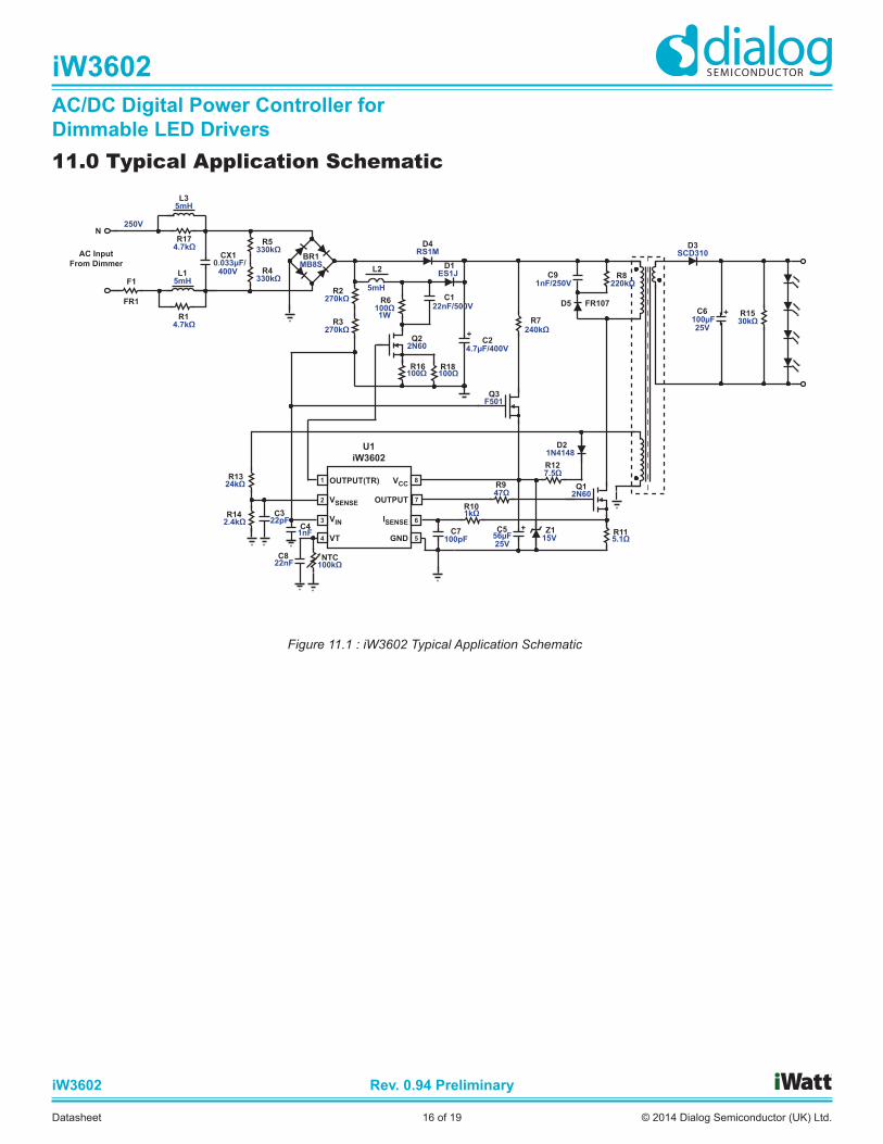
11.0 Typical Application Schematic
AC InputFrom Dimmer VOUT
RTN
+
U1iW3602
NTC
OUTPUT(TR)
VSENSE
VIN
VT
VCC
OUTPUT
ISENSE
GND
1
2
3
8
7
6
4 5
+
L35mH
R174.7kΩ
L15mH
R14.7kΩ
250V
CX10.033μF/
R2270kΩ
R3270kΩ
C41nF
R16100Ω
R6100Ω
D4RS1M
Q22N60 C2
4.7µF/400V
D3SCD310
C6100µF
R1530kΩ
R1324kΩ
R142.4kΩ
D21N4148
5.1ΩR11
Q12N60
BR1MB8S
Q3F501
R71W
+C556µF
7.5ΩR12
C7100pF
1kΩR10
47ΩR9
100kΩ
25V
R5330kΩ
R4330kΩ
R18100Ω
25V
Z115V
N
FR1
F1400V L2
5mHR8
220kΩC1
22nF/500V
C91nF/250V
D5 FR107
C322pF
C822nF
240kΩ
D1ES1J
Figure 11.1 : iW3602 Typical Application Schematic
iW3602AC/DC Digital Power Controller for Dimmable LED Drivers
Rev. 0.94 PreliminaryiW3602
© 2014 Dialog Semiconductor (UK) Ltd.Datasheet 17 of 19
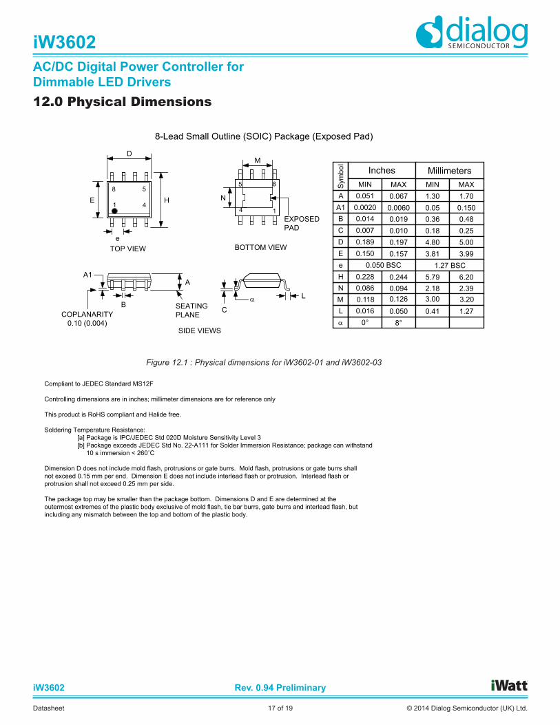
12.0 Physical Dimensions
Compliant to JEDEC Standard MS12F
Controlling dimensions are in inches; millimeter dimensions are for reference only
This product is RoHS compliant and Halide free.
Soldering Temperature Resistance: [a] Package is IPC/JEDEC Std 020D Moisture Sensitivity Level 3 [b] Package exceeds JEDEC Std No. 22-A111 for Solder Immersion Resistance; package can withstand 10 s immersion < 260˚C
Dimension D does not include mold flash, protrusions or gate burrs. Mold flash, protrusions or gate burrs shallnot exceed 0.15 mm per end. Dimension E does not include interlead flash or protrusion. Interlead flash or protrusion shall not exceed 0.25 mm per side.
The package top may be smaller than the package bottom. Dimensions D and E are determined at theoutermost extremes of the plastic body exclusive of mold flash, tie bar burrs, gate burrs and interlead flash, but including any mismatch between the top and bottom of the plastic body.
8-Lead Small Outline (SOIC) Package (Exposed Pad)
COPLANARITY0.10 (0.004)
8 5
41
SEATINGPLANE
A1
E H
B
D
e
A
C
Lα
5 8
14
N
M
EXPOSEDPAD
TOP VIEW BOTTOM VIEW
SIDE VIEWS
Inches
Sym
bol
MillimetersMIN
0.0020A1
MAX MIN MAX
0.0060 0.05 0.1500.051A 0.067 1.30 1.70
0.014B 0.019 0.36 0.480.007C 0.010 0.18 0.250.189D 0.197 4.80 5.000.150E 0.157 3.81 3.99
0.050 BSCe 1.27 BSC0.228H 0.244 5.79 6.200.086N 0.094 2.18 2.39
0.016L 0.050 0.41 1.270°α 8°
M 3.203.000.118 0.126
Figure 12.1 : Physical dimensions for iW3602-01 and iW3602-03

iW3602AC/DC Digital Power Controller for Dimmable LED Drivers
Rev. 0.94 PreliminaryiW3602
© 2014 Dialog Semiconductor (UK) Ltd.Datasheet 18 of 19
Figure 12.2 : Physical dimensions for iW3602-31 Compliant to JEDEC Standard MS12F
Controlling dimensions are in inches; millimeter dimensions are for reference only
This product is RoHS compliant and Halide free.
Soldering Temperature Resistance: [a] Package is IPC/JEDEC Std 020D Moisture Sensitivity Level 1 [b] Package exceeds JEDEC Std No. 22-A111 for Solder Immersion Resistance; package can withstand 10 s immersion < 260˚C
Dimension D does not include mold flash, protrusions or gate burrs. Mold flash, protrusions or gate burrs shallnot exceed 0.15 mm per end. Dimension E does not include interlead flash or protrusion. Interlead flash or protrusion shall not exceed 0.25 mm per side.
The package top may be smaller than the package bottom. Dimensions D and E are determined at theoutermost extremes of the plastic body exclusive of mold flash, tie bar burrs, gate burrs and interlead flash, but including any mismatch between the top and bottom of the plastic body.
8-Lead Small Outline (SOIC) Package
COPLANARITY0.10 (0.004)
8 5
41
SEATINGPLANE
A1
E H
B
D
e
A
C
Lα
TOP VIEW
SIDE VIEWS
Inches
Sym
bol
MillimetersMIN
0.0020A1
MAX MIN MAX
0.0060 0.05 0.1500.051A 0.067 1.30 1.70
0.014B 0.019 0.36 0.480.007C 0.010 0.18 0.250.189D 0.197 4.80 5.000.150E 0.157 3.81 3.99
0.050 BSCe 1.27 BSC0.228H 0.244 5.79 6.200.086N 0.094 2.18 2.39
0.016L 0.050 0.41 1.270°α 8°
M 3.203.000.118 0.126
Part Number Options Package Description
iW3602-01 Optimized for 230VAC Applications2 SOIC-8-EP3 Tape & Reel1
iW3602-03 Optimized for 100VAC Applications2
Supports high power factor (> 0.9 without dimmer) SOIC-8-EP3 Tape & Reel1
iW3602-31 Optimized for 230VAC Applications2, Improved Bleeder, Low Cost Package SOIC-8 Tape & Reel1
Note 1: Tape & Reel packing quantity is 2,500/reel. Minimum ordering quantity is 2,500.
Note 2: Refer to Section 9.4 Chopping Operation for more information.
Note 3: For the exposed pad package, refer to Section 9.13 Thermal Design.
13.0 Ordering Information

DisclaimerInformation in this document is believed to be accurate and reliable. However, Dialog Semiconductor does not give any representations or warranties, expressed or implied, as to the accuracy or completeness of such information. Dialog Semiconductor furthermore takes no responsibility whatsoever for the content in this document if provided by any information source outside of Dialog Semiconductor.
Dialog Semiconductor reserves the right to change without notice the information published in this document, including without limitation the specification and the design of the related semiconductor products, software and applications.
Applications, software, and semiconductor products described in this document are for illustrative purposes only. Dialog Semiconductor makes no representation or warranty that such applications, software and semiconductor products will be suitable for the specified use without further testing or modification. Unless otherwise agreed in writing, such testing or modification is the sole responsibility of the customer and Dialog Semiconductor excludes all liability in this respect.
Customer notes that nothing in this document may be construed as a license for customer to use the Dialog Semiconductor products, software and applications referred to in this document. Such license must be separately sought by customer with Dialog Semiconductor.
All use of Dialog Semiconductor products, software and applications referred to in this document are subject to Dialog Semiconductor’s Standard Terms and Conditions of Sale, unless otherwise stated.
© Dialog Semiconductor (UK) Ltd. All rights reserved.
RoHS complianceDialog Semiconductor complies to European Directive 2001/95/EC and from 2 January 2013 onwards to European Directive 2011/65/EU concerning Restriction of Hazardous Substances (RoHS/RoHS2). Dialog Semiconductor’s statement on RoHS can be found on the customer portal https://support.diasemi.com/. RoHS certificates from our suppliers are available on request.
Contacting Dialog SemiconductorUnited KingdomDialog Semiconductor (UK) LtdPhone: +44 1793 757700
GermanyDialog Semiconductor GmbHPhone: +49 7021 805-0
The NetherlandsDialog Semiconductor B.V.Phone: +31 73 640 88 22
North AmericaDialog Semiconductor Inc.Phone: +1 408 845 8500
JapanDialog Semiconductor K. K.Phone: +81 3 5425 4567
TaiwanDialog Semiconductor TaiwanPhone: +886 8178 6222
Web site: www.dialog-semiconductor.com
SingaporeDialog Semiconductor SingaporePhone: +65 64849929
Hong KongDialog Semiconductor Hong KongPhone: +852 2607 4271
KoreaDialog Semiconductor KoreaPhone: +82 2 3469 8200
ChinaDialog Semiconductor(Shenzhen)Phone: +86 755 2981 3669
Dialog Semiconductor(Shanghai)Phone: +86 21 5178 2561
iW3602AC/DC Digital Power Controller for Dimmable LED Drivers
Rev. 0.94 PreliminaryiW3602
© 2014 Dialog Semiconductor (UK) Ltd.Datasheet 19 of 19