Embed Size (px)
Citation preview

General DescriptionThe MAX5811 is a single, 10-bit voltage-output digital-to-analog converter (DAC) with an I2C™-compatible 2-wireinterface that operates at clock rates up to 400kHz. Thedevice operates from a single 2.7V to 5.5V supply anddraws only 100µA at VDD = 3.6V. A low-power power-down mode decreases current consumption to less than1µA. The MAX5811 features three software-selectablepower-down output impedances: 100kΩ, 1kΩ, and highimpedance. Other features include an internal precisionRail-to-Rail® output buffer and a power-on reset (POR)circuit that powers up the DAC in the 100kΩ power-downmode.The MAX5811 features a double-buffered I2C-compatibleserial interface that allows multiple devices to share a sin-gle bus. All logic inputs are CMOS-logic compatible andbuffered with Schmitt triggers, allowing direct interfacingto optocoupled and transformer-isolated interfaces. TheMAX5811 minimizes digital noise feedthrough by discon-necting the clock (SCL) signal from the rest of the devicewhen an address mismatch is detected.The MAX5811 is specified over the extended temperaturerange of -40°C to +85°C and is available in a space-sav-ing 6-pin SOT23 package. Refer to the MAX5812 datasheet for the 12-bit version.
ApplicationsDigital Gain and Offset AdjustmentsProgrammable Voltage and Current SourcesProgrammable AttenuationVCO/Varactor Diode ControlLow-Cost InstrumentationBattery-Operated Equipment
Features♦ Ultra-Low Supply Current
100µA at VDD = 3.6V130µA at VDD = 5.5V
♦ 300nA Low-Power Power-Down Mode
♦ Single 2.7V to 5.5V Supply Voltage
♦ Fast 400kHz I2C-Compatible 2-Wire SerialInterface
♦ Schmitt-Trigger Inputs for Direct Interfacingto Optocouplers
♦ Rail-to-Rail Output Buffer Amplifier
♦ Three Software-Selectable Power-Down OutputImpedances
100kΩ, 1kΩ, and High Impedance
♦ Read-Back Mode for Bus and Data Checking
♦ Power-On Reset to Zero
♦ Miniature 6-Pin SOT23 Package
MA
X5
81
1
10-Bit, Low-Power, 2-Wire Interface, Serial, Voltage-Output DAC
________________________________________________________________ Maxim Integrated Products 1
SCLSDA
1
2
6
5
VDD
ADDGND
OUT
MAX5811
SOT23
TOP VIEW
3 4
Pin Configuration
Ordering Information
RS
RS
RS
RS
RPRP
VDD
µCSDA SCL
SDA
SDA
SCL
SCL
VDD
VDD
VDD
OUT
OUT
MAX5811
MAX5811
Typical Operating Circuit
19-2270; Rev 1; 11/04
For pricing, delivery, and ordering information, please contact Maxim/Dallas Direct! at 1-888-629-4642, or visit Maxim’s website at www.maxim-ic.com.
PART TEMP RANGEPIN-PACKAGE
TOPMARK
MAX5811LEUT-T -40°C to +85°C 6 SOT23-6 AAYS
MAX5811MEUT-T -40°C to +85°C 6 SOT23-6 AAYU
MAX5811NEUT-T -40°C to +85°C 6 SOT23-6 AAYW
MAX5811PEUT-T -40°C to +85°C 6 SOT23-6 AAYY
Functional Diagram appears at end of data sheet.
Rail-to-Rail is a registered trademark of Nippon Motorola, Ltd.I2C is a trademark of Philips Corp.

MA
X5
81
1
10-Bit Low Power 2-Wire Interface Serial, Voltage-Output DAC
2 _______________________________________________________________________________________
ABSOLUTE MAXIMUM RATINGS
ELECTRICAL CHARACTERISTICS(VDD = +2.7V to +5.5V, GND = 0, RL = 5kΩ, CL = 200pF, TA = TMIN to TMAX, unless otherwise noted. Typical values are at VDD = +5V, TA = +25°C.) (Note 1)
Stresses beyond those listed under “Absolute Maximum Ratings” may cause permanent damage to the device. These are stress ratings only, and functionaloperation of the device at these or any other conditions beyond those indicated in the operational sections of the specifications is not implied. Exposure toabsolute maximum rating conditions for extended periods may affect device reliability.
VDD, SCL, SDA to GND............................................-0.3V to +6VOUT, ADD to GND........................................-0.3V to VDD + 0.3VMaximum Current into Any Pin............................................50mAContinuous Power Dissipation (TA = +70°C)
6-Pin SOT23 (derate 9.1mW above +70°C).................727mW
Operating Temperature Range ...........................-40°C to +85°CMaximum Junction Temperature .....................................+150°CStorage Temperature Range .............................-65°C to +150°CLead Temperature (soldering, 10s) .................................+300°C
PARAMETER SYMBOL CONDITIONS MIN TYP MAX UNITS
STATIC ACCURACY (Note 2)
Resolution N 10 Bits
Integral Nonlinearity INL (Note 3) ±0.5 ±4 LSB
Differential Nonlinearity DNL Guaranteed monotonic (Note 3) ±0.5 LSB
Zero-Code Error ZCE Code = 000 hex, VDD = 2.7V ±6 ±40 mV
Zero-Code Error Tempco 2.3 ppm/°C
Gain Error GE Code = 3FF hex -0.8 -3 %FS
Gain-Error Tempco 0.26 ppm/°C
DAC OUTPUT
Output Voltage Range No load (Note 4) 0 VDD V
DC Output Impedance Code = 200 hex 1.2 ΩVDD = 5V, VOUT = full scale (short to GND) 42.2
Short-Circuit CurrentVDD = 3V, VOUT = full scale (short to GND) 15.1
mA
VDD = 5V 8Wake-Up Time
VDD = 3V 8µs
DAC Output Leakage CurrentPower-down mode = high impedance,VDD = 5.5V, VOUT = VDD or GND
±0.1 ±1 µA
DIGITAL INPUTS (SCL, SDA)
Input High Voltage VIH0.7 xVDD
V
Input Low Voltage VIL0.3 xVDD
V
Input Hysteresis0.05 xVDD
V
Input Leakage Current Digital inputs = 0 or VDD ±0.1 ±1 µA
Input Capacitance 6 pF
DIGITAL OUTPUT (SDA)
Output Logic Low Voltage VOL ISINK = 3mA 0.4 V
Three-State Leakage Current IL Digital inputs = 0 or VDD ±0.1 ±1 µA
Three-State Output Capacitance 6 pF

MA
X5
81
1
10-Bit Low Power 2-Wire Interface Serial, Voltage-Output DAC
_______________________________________________________________________________________ 3
Note 1: All devices are 100% production tested at TA = +25°C and are guaranteed by design for TA = TMIN to TMAX.Note 2: Static specifications are tested with the output unloaded.Note 3: Linearity is guaranteed from codes 29 to 995.Note 4: Offset and gain error limit the FSR.Note 5: Guaranteed by design. Not production tested.
ELECTRICAL CHARACTERISTICS (continued)(VDD = +2.7V to +5.5V, GND = 0, RL = 5kΩ, CL = 200pF, TA = TMIN to TMAX, unless otherwise noted. Typical values are at VDD = +5V, TA = +25°C.) (Note 1)
PARAMETER SYMBOL CONDITIONS MIN TYP MAX UNITS
DYNAMIC PERFORMANCE
Voltage-Output Slew Rate SR 0.5 V/µs
Voltage-Output Settling TimeTo 1/2LSB code 100 hex to 300 hex or 300hex to 100 hex (Note 5)
4 12 µs
Digital Feedthrough Code = 000 hex, digital inputs from 0 to VDD 0.2 nV-s
Digital-to-Analog Glitch ImpulseMajor-carry transition (code = 1FF hex to 200hex and 200 hex to 1FF hex)
12 nV-s
POWER SUPPLIES
Supply Voltage Range VDD 2.7 5.5 V
All digital inputs at 0 or VDD = 3.6V 100 170Supply Current withNo Load All digital inputs at 0 or VDD = 5.5V 130 190
Power-Down Supply Current All digital inputs at 0 or VDD = 5.5V 0.3 1 µA
TIMING CHARACTERISTICS (Figure 1)
Serial Clock Frequency fSCL 0 400 kHz
Bus-Free Time Between STOPand START Conditions
tBUF 1.3 µs
START Condition Hold Time tHD,STA 0.6 µs
SCL Pulse Width Low tLOW 1.3 µs
SCL Pulse Width High tHIGH 0.6 µs
Repeated START Setup Time tSU,STA 0.6 µs
Data Hold Time tHD,DAT 0 0.9 µs
Data Setup Time tSU,DAT 100 ns
SDA and SCL ReceivingRise Time
tr (Note 5) 0 300 ns
SDA and SCL ReceivingFall Time
tf (Note 5) 0 300 ns
SDA Transmitting Fall Time tf (Note 5)20 +0.1Cb
250 ns
STOP Condition Setup Time tSU,STO 0.6 µs
Bus Capacitance Cb (Note 5) 400 pF
Maximum Duration ofSuppressed Pulse Widths
tSP 0 50 ns

MA
X5
81
1
10-Bit Low Power 2-Wire Interface Serial, Voltage-Output DAC
4 _______________________________________________________________________________________
-1.00
-0.75
-0.50
-0.25
0
0.25
0.50
0.75
1.00
0 256 512 768 1024
INTEGRAL NONLINEARITYvs. INPUT CODE
MAX
5811
toc0
1
INPUT CODE
INTE
GRAL
NON
LINE
ARIT
Y (L
SB)
0
0.25
0.75
0.50
1.00
1.25
INTEGRAL NONLINEARITYvs. SUPPLY VOLTAGE
MAX
5811
toc0
2
SUPPLY VOLTAGE (V)
INTE
GRAL
NON
LINE
ARIT
Y (L
SB)
2.7 4.13.4 4.8 5.50
0.25
0.75
0.50
1.00
1.25
-40 10-15 35 60 85
INTEGRAL NONLINEARITYvs. TEMPERATURE
MAX
5811
toc0
3
TEMPERATURE (°C)
INTE
GRAL
NON
LINE
ARIT
Y (L
SB)
-1.00
-0.75
-0.50
-0.25
0
0.25
0.50
0.75
1.00
0 256 512 768 1024
DIFFERENTIAL NONLINEARITYvs. INPUT CODE
MAX
5811
toc0
4
INPUT CODE
DIFF
EREN
TIAL
NON
LINE
ARIT
Y (L
SB)
-0.5
-0.4
-0.2
-0.3
-0.1
0
DIFFERENTIAL NONLINEARITYvs. SUPPLY VOLTAGE
MAX
5811
toc0
5
SUPPLY VOLTAGE (V)
DIFF
EREN
TIAL
NON
LINE
ARIT
Y (L
SB)
2.7 4.13.4 4.8 5.5-0.5
-0.4
-0.2
-0.3
-0.1
0
-40 10-15 35 60 85
DIFFERENTIAL NONLINEARITYvs. TEMPERATURE
MAX
5811
toc0
6
TEMPERATURE (°C)
DIFF
EREN
TIAL
NON
LINE
ARIT
Y (L
SB)
0
2
6
4
8
10
ZERO-CODE ERRORvs. SUPPLY VOLTAGE
MAX
8511
toc0
7
SUPPLY VOLTAGE (V)
ZERO
-COD
E ER
ROR
(mV)
2.7 4.13.4 4.8 5.5
NO LOAD
0
2
6
4
8
10
-40 10-15 35 60 85
ZERO-CODE ERROR vs. TEMPERATURE
MAX
5811
toc0
8
TEMPERATURE (°C)
ZERO
-COD
E ER
ROR
(mV)
NO LOAD
0
-0.4
-1.2
-0.8
-1.6
-2.0
GAIN ERRORvs. SUPPLY VOLTAGE
MAX
5811
toc0
9
SUPPLY VOLTAGE (V)
GAIN
ERR
OR (%
FSR)
2.7 4.13.4 4.8 5.5
NO LOAD
Typical Operating Characteristics(VDD = +5V, RL = 5kΩ, TA = +25°C.)

MA
X5
81
1
10-Bit Low Power 2-Wire Interface Serial, Voltage-Output DAC
_______________________________________________________________________________________ 5
0
-0.4
-1.2
-0.8
-1.6
-2.0
-40
NO LOAD
10-15 35 60 85
GAIN ERROR vs. TEMPERATURE
MAX
5811
toc1
0
TEMPERATURE (°C)
GAIN
ERR
OR (%
FSR)
0
2
1
4
3
5
6
0 10
DAC OUTPUT VOLTAGEvs. OUTPUT SOURCE CURRENT (NOTE 6)
MAX
5811
toc1
1
OUTPUT SOURCE CURRENT (mA)
DAC
OUTP
UT V
OLTA
GE (V
)
42 6 8
CODE = 3FF hex
0
0.5
1.5
1.0
2.0
2.5
0 42 6 8 10
DAC OUTPUT VOLTAGE vs. OUTPUT SINK CURRENT (NOTE 6)
MAX
5811
roc1
2
OUTPUT SINK CURRENT (mA)
DAC
OUTP
UT V
OLTA
GE (V
)
CODE = 100 hex
0
40
20
80
60
100
120
0 512256 768 1024
SUPPLY CURRENTvs. INPUT CODE
MAX
5811
toc1
3
INPUT CODE
SUPP
LY C
URRE
NT (µ
A)
NO LOAD
100
95
90
85
80-40 10-15 35 60 85
SUPPLY CURRENTvs. TEMPERATURE
MAX
5811
toc1
4
TEMPERATURE (°C)
SUPP
LY C
URRE
NT (µ
A)
NO LOADCODE = 3FF hex
50
60
80
70
90
100
SUPPLY CURRENTvs. SUPPLY VOLTAGE
MAX
5811
toc1
5
SUPPLY VOLTAGE (V)
SUPP
LY C
URRE
NT (µ
A)
2.5 4.53.5 5.5
CODE = 3FF hexNO LOAD
0
100
300
200
400
500
POWER-DOWN SUPPLY CURRENTvs. SUPPLY VOLTAGE
MAX
5811
1 to
c16
SUPPLY VOLTAGE (V)
POW
ER-D
OWN
SUPP
LY C
URRE
NT (n
A)
2.7 4.13.4 4.8 5.5
ZOUT = HIGH IMPEDANCENO LOAD
TA = +25°CTA = -40°C
TA = +85°C OUT
5V
0
10mV/div
VDD
100µs/div
POWER-UP GLITCHMAX5811 toc17
EXITING SHUTDOWNMAX5811 toc18
500mV/divOUT
2µs/divCLOAD = 200pF CODE = 200 hex
Typical Operating Characteristics (continued)(VDD = +5V, RL = 5kΩ, TA = +25°C.)

MA
X5
81
1
10-Bit Low Power 2-Wire Interface Serial, Voltage-Output DAC
6 _______________________________________________________________________________________
Typical Operating Characteristics (continued)(VDD = +5V, RL = 5kΩ, TA = +25°C.)
OUT
5V
0
10mV/div
VDD
100µs/div
MAJOR-CARRY TRANSITION(POSITIVE)
MAX5811 toc19
MAJOR-CARRY TRANSITION(NEGATIVE)
MAX5811 toc20
5mV/divOUT
2µs/divCLOAD = 200pFRL = 5kΩ
CODE = 200 hex to 1FF hex
SETTLING TIME(POSITIVE)
MAX5811 toc21
500mV/divOUT
2µs/divCLOAD = 200pF CODE = 100 hex to 300 hex
SETTLING TIME(NEGATIVE)
MAX5811 toc22
500mV/divOUT
2µs/divCLOAD = 200pF CODE = 300 hex to 100 hex
DIGITAL FEEDTHROUGHMAX5811 toc23
CLOAD = 200pFfSCL = 12kHz
CODE = 000 hex
Note 6: The ability to drive loads less than 5kΩ is not implied.

MA
X5
81
1
10-Bit Low Power 2-Wire Interface Serial, Voltage-Output DAC
_______________________________________________________________________________________ 7
Detailed DescriptionThe MAX5811 is a 10-bit, voltage-output DAC with anI2C/SMBus-compatible 2-wire interface. The deviceconsists of a serial interface, power-down circuitry,input and DAC registers, a 10-bit resistor string DAC,unity-gain output buffer, and output resistor network.The serial interface decodes the address and controlbits, routing the data to either the input or DAC register.Data can be directly written to the DAC register imme-diately updating the device output, or can be written tothe input register without changing the DAC output.Both registers retain data as long as the device is pow-ered.
DAC OperationThe MAX5811 uses a segmented resistor string DACarchitecture, which saves power in the overall systemand guarantees output monotonicity. The MAX5811’sinput coding is straight binary, with the output voltagegiven by the following equation:
where N = 10 (bits), and D = the decimal value of theinput code (0 to 1023).
Output BufferThe MAX5811 analog output is buffered by a precision,unity-gain follower that slews at about 0.5V/µs. The
buffer output swings rail-to-rail, and is capable of dri-ving 5kΩ in parallel with 200pF. The output settles to±0.5LSB within 4µs.
Power-On ResetThe MAX5811 features an internal POR circuit that ini-tializes the device upon power-up. The DAC registersare set to zero scale and the device is powered-downwith the output buffer disabled and the output pulled toGND through the 100kΩ termination resistor. Followingpower-up, a wake-up command must be initiatedbefore any conversions are performed.
Power-Down ModesThe MAX5811 has three software-controlled low-powerpower-down modes. All three modes disable the outputbuffer and disconnect the DAC resistor string from VDD,reducing supply current draw to 300nA. In power-downmode 0, the device output is high impedance. Inpower-down mode 1, the device output is internallypulled to GND by a 1kΩ termination resistor. In power-down mode 2, the device output is internally pulled toGND by a 100kΩ termination resistor. Table 1 showsthe power-down mode command words.
Upon wake-up, the DAC output is restored to its previ-ous value. Data is retained in the input and DAC regis-ters during power-down mode.
Digital Interface The MAX5811 features an I2C/SMBus-compatible 2-wire interface consisting of a serial data line (SDA) and
VV D
OUTREF
N=×( )
2
Pin Description
PIN NAME FUNCTION
1 VDD Power Supply and DAC Reference Input
2 GND Ground
3 SDA Bidirectional Serial Data I/O
4 SCL Serial Clock Line
5 ADD Address Select. A logic high sets the address LSB to 1, a logic low sets the address LSB to 0.
6 OUT Analog Output
Table 1. Power-Down Command Bits
POWER-DOWNCOMMAND BITS
PD1 PD0
MODE/FUNCTION
0 0 Power-up device. DAC output restored to previous value.
0 1 Power-down mode 0. Power-down device with output floating.
1 0 Power-down mode 1. Power-down device with output terminated with 1kΩ to GND.
1 1 Power-down mode 2. Power-down device with output terminated with 100kΩ to GND.

MA
X5
81
1
10-Bit Low Power 2-Wire Interface Serial, Voltage-Output DAC
8 _______________________________________________________________________________________
a serial clock line (SCL). The MAX5811 is SMBus com-patible within the range of VDD = 2.7V to 3.6V. SDA andSCL facilitate bidirectional communication between theMAX5811 and the master at rates up to 400kHz. Figure1 shows the 2-wire interface timing diagram. TheMAX5811 is a transmit/receive slave-only device, rely-ing upon a master to generate a clock signal. The mas-ter (typically a microcontroller) initiates data transfer onthe bus and generates SCL to permit that transfer.
A master device communicates to the MAX5811 bytransmitting the proper address followed by commandand/or data words. Each transmit sequence is framedby a START (S) or REPEATED START (Sr) condition anda STOP (P) condition. Each word transmitted over thebus is 8 bits long and is always followed by anacknowledge clock pulse.
The MAX5811 SDA and SCL drivers are open-drainoutputs, requiring a pullup resistor (500Ω or greater) togenerate a logic high voltage (see Typical OperatingCircuit). Series resistors RS are optional. These seriesresistors protect the input stages of the MAX5811 fromhigh-voltage spikes on the bus lines, and minimizecrosstalk and undershoot of the bus signals.
Bit TransferOne data bit is transferred during each SCL clockcycle. The data on SDA must remain stable during thehigh period of the SCL clock pulse. Changes in SDAwhile SCL is high are control signals (see START andSTOP Conditions). SDA and SCL idle high when the I2C bus is not busy. START and STOP Conditions
When the serial interface is inactive, SDA and SCL idlehigh. A master device initiates communication by issu-ing a START condition. A START condition is a high-to-
Figure 1. 2-Wire Serial lnterface Timing Diagram
SCL
SDA
STOPCONDITION
STARTCONDITION
REPEATED START CONDITIONSTART CONDITION
tLOW
tSU, DATtSU, STA
tSP
tBUFtHD, STAtSU, STO
tR tFtHD, STA
tHIGH
tHD, DAT
SCL
SDA
S Sr P
Figure 2. START/STOP Conditions
Figure 3. Early STOP Condition
SCL
SDA
STOP START
SCL
SDA
ILLEGALSTOP
START
ILLEGAL EARLY STOP CONDITION
LEGAL STOP CONDITION
MA
X5
81
1
10-Bit Low Power 2-Wire Interface Serial, Voltage-Output DAC
_______________________________________________________________________________________ 9
low transition on SDA with SCL high. A STOP conditionis a low-to-high transition on SDA while SCL is high(Figure 2). A START condition from the master signalsthe beginning of a transmission to the MAX5811. Themaster terminates transmission by issuing a notacknowledge followed by a STOP condition (seeAcknowledge Bit). The STOP condition frees the bus. Ifa repeated START condition (Sr) is generated instead ofa STOP condition, the bus remains active. When aSTOP condition or incorrect address is detected, theMAX5811 internally disconnects SCL from the serialinterface until the next START condition, minimizing digi-tal noise and feedthrough.
Early STOP ConditionsThe MAX5811 recognizes a STOP condition at any pointduring transmission except if a STOP condition occurs inthe same high pulse as a START condition (Figure 3).This condition is not a legal I2C format; at least oneclock pulse must separate any START and STOP condi-tions.
Repeated START ConditionsA REPEATED START (Sr) condition may indicate achange of data direction on the bus. Such a changeoccurs when a command word is required to initiate aread operation. Sr may also be used when the busmaster is writing to several I2C devices and does notwant to relinquish control of the bus. The MAX5811 ser-ial interface supports continuous write operations withor without an Sr condition separating them. Continuousread operations require Sr conditions because of thechange in direction of data flow.
Acknowledge Bit (ACK)The acknowledge bit (ACK) is the ninth bit attached toany 8-bit data word. ACK is always generated by thereceiving device. The MAX5811 generates an ACKwhen receiving an address or data by pulling SDA lowduring the ninth clock period. When transmitting data,the MAX5811 waits for the receiving device to generatean ACK. Monitoring ACK allows for detection of unsuc-cessful data transfers. An unsuccessful data transferoccurs if a receiving device is busy or if a system faulthas occurred. In the event of an unsuccessful datatransfer, the bus master should reattempt communica-tion at a later time.
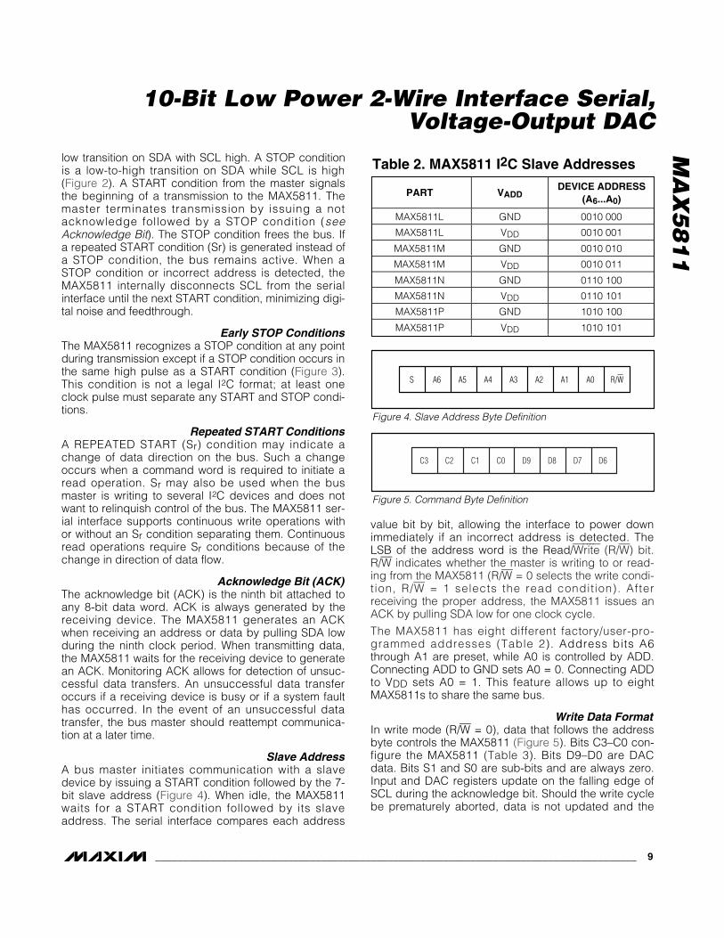
Slave AddressA bus master initiates communication with a slavedevice by issuing a START condition followed by the 7-bit slave address (Figure 4). When idle, the MAX5811waits for a START condition followed by its slaveaddress. The serial interface compares each address
value bit by bit, allowing the interface to power downimmediately if an incorrect address is detected. TheLSB of the address word is the Read/Write (R/W) bit.R/W indicates whether the master is writing to or read-ing from the MAX5811 (R/W = 0 selects the write condi-t ion, R/W = 1 selects the read condition). Afterreceiving the proper address, the MAX5811 issues anACK by pulling SDA low for one clock cycle.
The MAX5811 has eight different factory/user-pro-grammed addresses (Table 2). Address bits A6through A1 are preset, while A0 is controlled by ADD.Connecting ADD to GND sets A0 = 0. Connecting ADDto VDD sets A0 = 1. This feature allows up to eightMAX5811s to share the same bus.
Write Data FormatIn write mode (R/W = 0), data that follows the addressbyte controls the MAX5811 (Figure 5). Bits C3–C0 con-figure the MAX5811 (Table 3). Bits D9–D0 are DACdata. Bits S1 and S0 are sub-bits and are always zero.Input and DAC registers update on the falling edge ofSCL during the acknowledge bit. Should the write cyclebe prematurely aborted, data is not updated and the
S A6 A5 A4 A3 A2 A1 A0 R/W
Figure 4. Slave Address Byte Definition
Table 2. MAX5811 I2C Slave Addresses
PART VADDDEVICE ADDRESS
(A6...A0)
MAX5811L GND 0010 000
MAX5811L VDD 0010 001
MAX5811M GND 0010 010
MAX5811M VDD 0010 011
MAX5811N GND 0110 100
MAX5811N VDD 0110 101
MAX5811P GND 1010 100
MAX5811P VDD 1010 101
C3 C2 C1 C0 D9 D8 D7 D6
Figure 5. Command Byte Definition

MA
X5
81
1
10-Bit Low Power 2-Wire Interface Serial, Voltage-Output DAC
10 ______________________________________________________________________________________
write cycle must be repeated. Figure 6 shows twoexample write data sequences.
Read Data FormatIn read mode (R/W = 1), the MAX5811 writes the con-tents of the DAC register to the bus. The direction of
Table 3. Command Byte DefinitionsSERIAL DATA INPUT
C3 C2 C1 C0 D9/PD1* D8/PD0* D7-D6FUNCTION
1 1 0 0DACDATA
DACDATA
DACDATA
Load DAC with new data from the following data byte andupdate DAC output simultaneously as soon as data isavailable from the serial bus. The DAC and input registersare updated with the new data.
1 1 0 1DACDATA
DACDATA
DACDATA
Load input register with data from the following data byte.DAC output remains unchanged.
1 1 1 0DACDATA
DACDATA
DACDATA
Load input register with data from the following data byte.Update DAC output to the previously stored data.
1 1 1 1 X X XXUpdate DAC output from input register. The deviceignores any new data.
1 0 X X X X XXRead data request. Data bits are ignored. The contents ofthe DAC register are available on the bus.
0 1 X X 0 0 XX Power up the device.
0 1 X X 0 1 XXPower-down mode 0. Power down device with outputfloating.
0 1 X X 1 0 XXPower-down mode 1. Power down device with outputterminated with 1kΩ to GND.
0 1 X X 1 1 XXPower-down mode 2. Power down device with outputterminated with 100kΩ to GND.
S
MSB
MSB
A6 A5 A4 A3 A2 A1 A0 C3 C2 C1 C0 D9 D8 D7 D6
D5 D4 D3 D2 D1 D0 S1 S0 P
R/W ACK
ACK
ACK
LSB MSB LSB
LSB
S
MSB
A6 A5 A4 A3 A2 A1 A0 C3 C2 X X PD1 PD0 X X PR/W ACK ACK
LSB
EXAMPLE WRITE DATA SEQUENCE
EXAMPLE WRITE TO POWER-DOWN REGISTER SEQUENCE
MSB
LSB
Figure 6. Example Write Command Sequences
*When C3 = 0 and C2 = 1, data bits D9 and D8 write to the power-down registers (PD1 and PD0).X = Don’t care.

MA
X5
81
1
10-Bit Low Power 2-Wire Interface Serial, Voltage-Output DAC
______________________________________________________________________________________ 11
data flow reverses following the address acknowledgeby the MAX5811. The device transmits the first byte ofdata, waits for the master to acknowledge, then trans-mits the second byte. Figure 7 shows an example readdata sequence.
I2C CompatibilityThe MAX5811 is compatible with existing I2C systems.SCL and SDA are high-impedance inputs; SDA has anopen drain that pulls the data line low during the ninthclock pulse. The Typical Operating Circuit shows a typ-ical I2C application. The communication protocol sup-ports the standard I2C 8-bit communications. Thegeneral call address is ignored. The MAX5811 addressis compatible with the 7-bit I2C addressing protocolonly. No 10-bit address formats are supported.
Digital Feedthrough SuppressionWhen the MAX5811 detects an address mismatch, theserial interface disconnects the SCL signal from thecore circuitry. This minimizes digital feedthroughcaused by the SCL signal on a static output. The serialinterface reconnects the SCL signal once a validSTART condition is detected.
Applications InformationPowering the Device from an
External ReferenceThe MAX5811 uses the VDD as the DAC voltage refer-ence. Any power-supply noise is directly coupled to thedevice output. The circuit in Figure 8 uses a precisionvoltage reference to power the MAX5811, isolating thedevice from any power-supply noise. Powering theMAX5811 in such a manner greatly improves overallperformance, especially in noisy systems. TheMAX6030 (3V, 75ppm/°C) or the MAX6050 (5V,75ppm/°C) precision voltage references are idealchoices due to the low power requirements of theMAX5811.
Digital Inputs and Interface LogicThe MAX5811 2-wire digital interface is I2C and SMBuscompatible. The two digital inputs (SCL and SDA) loadthe digital input serially into the DAC. Schmitt-triggerbuffered inputs allow slow-transition interfaces such as
S A6 A5 A4 A3 A2 A1 A0 C3 C2 X X X X X X
Sr A6 A5 A4 A3 A2 A1 A0
MSB LSB MSB LSB
LSBMSB
ACK ACK
ACK
D5 D4 D3 D2 D1 D0 X X
MSB LSB
ACK
ACK P
R/W = 1 X X PD1 PD0 D9 D8 D7 D6
MSB LSB
DATA BYTES GENERATED BY MASTER DEVICE
DATA BYTES GENERATED BY MAX5811ACK GENERATED BY
MASTER DEVICE
R/W = 0
Figure 7. Read Word Data Sequence
VDD
IN
GNDGND
OUT
OUTMAX5811MAX6030/MAX6050
Figure 8. Powering the MAX5811 from an External Reference

MA
X5
81
1
optocouplers to interface directly to the device. Thedigital inputs are compatible with CMOS logic levels.
Power-Supply Bypassing and Ground Management
Careful PC board layout is important for optimal systemperformance. Keep analog and digital signals separateto reduce noise injection and digital feedthrough. Use aground plane to ensure that the ground return fromGND to the power-supply ground is short and lowimpedance. Bypass VDD with a 0.1µF capacitor toground as close to the device as possible.
Chip InformationTRANSISTOR COUNT: 7172
PROCESS: BiCMOS
10-Bit Low Power 2-Wire Interface Serial, Voltage-Output DAC
12 ______________________________________________________________________________________
10-BITDAC
INPUTREGISTER
MUX AND DACREGISTER
RESISTORNETWORK
POWER-DOWNCIRCUITRY
SERIALINTERFACE
VDD
SDA ADD SCL GND
OUT
MAX5811
Functional Diagram
Selector GuidePART ADDRESS
MAX5811LEUT 0010 00X
MAX5811MEUT 0010 01X
MAX5811NEUT 0110 10X
MAX5811PEUT 1010 10X

MA
X5
81
1
10-Bit Low Power 2-Wire Interface Serial, Voltage-Output DAC
Maxim cannot assume responsibility for use of any circuitry other than circuitry entirely embodied in a Maxim product. No circuit patent licenses areimplied. Maxim reserves the right to change the circuitry and specifications without notice at any time.
Maxim Integrated Products, 120 San Gabriel Drive, Sunnyvale, CA 94086 408-737-7600 ____________________ 13
© 2004 Maxim Integrated Products Printed USA is a registered trademark of Maxim Integrated Products.
6LS
OT.
EP
S
Package Information(The package drawing(s) in this data sheet may not reflect the most current specifications. For the latest package outline informationgo to www.maxim-ic.com/packages.)