Embed Size (px)
Citation preview

This is the author’s version1 of a work that was accepted for publication in the following
source: IEEE Transactions on Microwave Theory and Techniques (T-MTT)
A Package-Integrated Chireix Outphasing RF
Switch-Mode High-Power Amplifier
By David A. Calvillo-Cortes, Mark P. van der Heijden, Mustafa Acar,
Michel de Langen, Robin Wesson, Fred van Rijs, and Leo C. N. de Vreede
This file was downloaded from: the HEECS consortium website http://www.heecs.eu/
Copyright 2013 IEEE
Notice: Changes introduced as a result of the publishing process, such as editing and
formatting may not be reflected in this document. For the final version of this work,
please refer to the published source: http://dx.doi.org/10.1109/TMTT.2013.2279372
1 This is an updated version correcting minor typos in the published paper. These typos will be reported to
IEEE in due time.

IEEE TRANSACTIONS ON MICROWAVE THEORY AND TECHNIQUES 1
A Package-Integrated Chireix Outphasing RFSwitch-Mode High-Power Amplifier
David A. Calvillo-Cortes, Student Member, IEEE, Mark P. van der Heijden, Member, IEEE, Mustafa Acar, Michelde Langen, Robin Wesson, Fred van Rijs and Leo C. N. de Vreede, Senior Member, IEEE
Abstract—This paper describes the design and implementationof a package-integrated Chireix outphasing RF switch-modepower amplifier. The optimum loading conditions, based onclass-E, and the Chireix compensation elements are providedto the active devices by a dedicated low-loss bondwire-basedtransformer power combiner that enables a very small formfactor and low cost. The realized prototype achieved 70.6 Wpeak power with 73% peak drain-efficiency at 2.3 GHz and28 V, and up to 81% peak drain-efficiency at 2.2 GHz and 20 V.When operated for maximum power at 28 V, it reached 53.5%/ 43.5% average drain / total-efficiency for a 9.6 dB PAR W-CDMA signal at 2.3 GHz with low ACLR1/2 levels (-49/-56 dBcafter memoryless DPD). Moreover, from 2.1-2.4 GHz, the realizedPA demonstrated more than 50% drain-efficiency across >260,>160 and >80 MHz at 6, 8 and 10 dB back-off, respectively.
Index Terms—Outphasing transmitter, base station, poweramplifier, Chireix combiner, broadband, transformer, bondwire,Class-E, switch-mode.
I. INTRODUCTION
NEXT generation base stations need to support multi-channel and multi-standard operation to reduce infras-
tructure costs. In addition, they must be energy-efficient inorder to reduce operational costs. These tasks are especiallychallenging for the power amplifier (PA) in the transmitter,since high average efficiency is required for high peak-to-average-power-ratio (PAR) and wideband complex modulatedsignals. Various PA efficiency enhancement techniques havebeen proposed over time [1], [2]. The most interesting con-cepts are based on either supply-voltage modulation, such asEnvelope Elimination and Restoration (EER) and EnvelopeTracking (ET) [2], or based on load modulation, such asOutphasing [3], [4] and Doherty [5]; each with their owninherent advantages and disadvantages.
Traditionally, Doherty and supply-voltage modulation tech-niques have been favoured by base station PA designers.The Doherty concept is a low-complexity and cost-effectivetechnique that has shown good efficiency [6] but typicallysuffers from a narrow operational RF bandwidth and therequirement for linear PAs in the branch amplifiers. Althoughthe first problem is being actively addressed [7], [8], the
D. A. Calvillo-Cortes and L. C. N. de Vreede are with the ElectronicsResearch Laboratory/Delft Institute of Microsystems and Nanoelectronics(DIMES), Delft University of Technology, 2628CD Delft, The Netherlands(e-mails: [email protected], [email protected]).
M. P. van der Hiejden and M. Acar are with NXP Semiconductors N.V.,5600KA Eindhoven, The Netherlands (email: [email protected]).
M. de Langen, R. Wesson and F. van Rijs are with NXP SemiconductorsN.V., 6534AE Nijmegen, The Netherlands.
Fig. 1. Package-integrated Chireix outphasing RF high-power amplifier.
latter requirement often results in a lower achievable peakefficiency. Amplifiers with supply-voltage modulation can alsooffer good efficiency (EER even allow switch-mode PAs forhigher efficiency) and a higher operational RF bandwidthdue to the lower complexity of the RF amplifying stage[9], [10]. However, they require an energy-efficient supplymodulator that in practice restricts the instantenous modulationbandwidth, yielding complications when aiming for widebandmulti-channel operation. Although the design of such a supplymodulator is improving [11], it still remains as an importantissue for the upcoming modulation schemes that tend tooccupy wider bandwidths.
In contrast, the outphasing amplifier [3] has been less popu-lar until recently. Outphasing is re-gaining attention due to ad-vances on low-power and high-speed digital signal processingand because it can be broadband [12], reconfigurable/multi-mode [13], [14] and can potentially bridge the gap betweenthe high power analog and digital domains [12]. The out-phasing concept can employ true switch-mode PAs (SMPAs)to increase the peak efficiency while still providing linearamplification [15]. In fact, different from Doherty and supply-voltage modulation, the linearity of the outphasing amplifierdoes not depend on the constitutive PAs themselves but ratheron the integrity of an amplitude to phase conversion [2] whichcan be accurately controlled at baseband.
A key component for the outphasing RF amplifier is thepower combiner. Previous work has mainly focused on im-plementing such combiner with transmission lines [16]–[19],where the usual Chireix compensation elements were eitherlumped or incorporated in the combiner [16], [18]. However,this approach is restricted in bandwidth due to the transmissionline-based combiner itself [20], although such implementation

IEEE TRANSACTIONS ON MICROWAVE THEORY AND TECHNIQUES 2
is not fundamental to the original concept. More recent workhas focused on transformer-based combiners [12]–[14], [20]–[22] and has reported in fact larger RF bandwidth, especiallyat deep back-off power levels [12], [22]. When considering theoperating class of the branch amplifiers, SMPAs have becomemore broadly used in outphasing amplifiers; such as voltage-mode class-D [13], [14] and class-E [12], [16], [20]–[23]. Forhigh-power, class-E has been identified as a good candidatefor the branch PAs, demonstrating high efficiency over awide dynamic range [16] and even broadband digital CMOScircuitry has been introduced for driving GaN SMPAs directly[12]. Furthermore, N-way outphasing has been proposed as amethod to increase efficiency at larger back-off levels by usinga non-Chireix combining strategy and four PAs [24], [25].
In [22], we proposed the first package-integrated implemen-tation of a high-power outphasing amplifier (see Fig. 1) thatfairly competes with the state-of-art PAs, including Dohertyand ET amplifiers. In this paper, we provide the necessaryunderlying theory and the detailed design considerations thatenabled such an amplifier. In Section II, we first review thebasic (broadband) outphasing concept from standard literature(e.g. [2], [4]) and then we complement such a theory witha more general expression for efficiency. With this we showthat from the (2-way) outphasing concept, higher efficiency,especially at deep back-off, can be obtained than what istraditionally considered. Then, as a proof of this importantaspect, the theoretical performance of the amplifier introducedin [22] is provided and discussed, clearly showing its efficiencyadvantage. Next, Section III describes its actual implementa-tion and finally Section IV provides its measurement results,now also including RF bandwidth performance as well as adescription of the employed digital pre-distortion.
II. BROADBAND OUTPHASING SWITCH-MODE AMPLIFIER
A. Broadband outphasing combiner
In an outphasing transmitter [3], see Fig. 2, the inputsignal is split (by a signal component separator, SCS) intotwo constant envelope signals, whose relative phase-differencecontains the original amplitude information. These signals areamplified by the branch amplifiers and vector summed at theiroutputs, yielding an amplified replica of the original inputsignal. As such, the outphasing concept can provide linearamplification using nonlinear components (also referred toas LINC [15]). In addition, its efficiency can be enhancedin power back-off operation by using a non-isolating power
θ(t) = sin-1( E(t) ) VoutV1
V2
-V2
VPA
θθV1
V2
VoutVin
Vout(t) = V1(t) – V2(t)Vin(t) = E(t)·e j φ(t)
V1,2(t) = VPA(t)·e j [φ(t) ± θ(t)]
cos(ωC·t)
PA
arcsin
PAφ(t)-θ(t)
φ(t)+θ(t)
VPA(t) = VPA·e j ω tc
S.C.S.
ω tc
Vout(t) Vin(t)·e jω tc
Fig. 2. Outphasing amplifier concept [3], [4] with equivalent phasor repre-sentation.
(a) (b)
Fig. 3. Principle of wideband Chireix combiner: a) with a floating load, b)with a transformer-based combiner.
combiner and two compensating elements (for the reactiveloading that occur at the output of each branch amplifier dueto the outphasing action), as proposed by Chireix [3].
Due to the bandwidth restriction imposed by (quarter-wavelength) transmission line-based power combiners [20],a wideband outphasing transmitter preferably delivers itspower into a broadband floating load or, equivalently, to atransformer-based combiner, as shown in Fig. 3. In that figure,the branch amplifiers are considered ideal voltage sourcesV1,2. The dynamic (time-dependent) admittance seen by eachof those branch amplifiers is given by [2], [4]:
Y1,2 (θ(t)) = G (θ(t))± j [B (θ(t))−Bθc1,2] (1)
in which
G (θ(t)) =
(1
RPA
)sin2 (θ(t)) (2)
B (θ(t)) =
(1
RPA
)sin (2 · θ(t))
2(3)
Bθc1,2 = B (θc1,2) (4)
where θ(t) is the dynamic outphasing angle, RPA is the loadseen by each amplifier at full power (i.e., when θ(t) = π
2 ),θc1,2 and Bθc1,2 are the Chireix compensating angles and sus-ceptances for branch 1 and 2, respectively. For the combinersin Fig. 3a and Fig. 3b, RPA = RL
2 and RPA =(
1T 2
)RL
2 ,respectively, where T is the transformer’s turns ratio.
B. Efficiency of the outphasing amplifier
The efficiency of the outphasing amplifier depends onboth its branch amplifiers and its power combining network.Starting with the original paper by Chireix [3], most previousworks have assumed that the maximum achievable efficiency ofthe outphasing amplifier, normalized with respect to the branchamplifier’s peak efficiency, equals solely the power factor(PF)1 of its power combiner. This is a reasonable assumptionfor linear branch amplifiers, like class-B (e.g. [4], [24]).However, even higher efficiencies (than anticipated solely bythe PF) can be reached with SMPA branch amplifiers, such asclass-E [12], [16]. In order to explain this, we need to reviewthe expression for (drain-) efficiency in outphasing amplifiers.
1A power factor indicates how much of the power delivered by a sourceis really utilized by its load (with 1 as maximum value), where the unusedpower can, but not necessarily will, induce losses.

IEEE TRANSACTIONS ON MICROWAVE THEORY AND TECHNIQUES 3
Hence, in this section we first derive a general expression forefficiency starting from basic principles. Then, we discuss theroles of different amplifier classes and the power combiner.
The total drain-efficiency ηDENfor N sources (e.g., power
amplifiers) combining their powers in a lossless manner canbe defined as the ratio of the total RF power
∑PRFn
at thefundamental frequency to the total DC power
∑PDCn
of thesources, this is
ηDEN=
∑Nn=1 PRFn∑Nn=1 PDCn
(5)
where the sub-index n refers to the n-source. In turn, PRFn
can be defined in terms of fundamental currents and voltages,or even admittances (or impedances), as
PRFn =1
2Re Vn · I∗n =
1
2|Vn|2 ·Re Yn (6)
PDCn= VDCn
· IDCn=
(VDCn
|Vn|IDCn
|In|
)· |Vn|2·|Yn| (7)
where the sub-index n refers to the fundamental voltage,current or admittance of each n-source. In the ideal outphasingPA concept2, the sources are considered identical and there-fore, from Eqs. 5-7, ηDEN
can be simplified to
ηDEN= ηS · PFN (8)
ηS =1
2
|Vn|VDCn
|In|IDCn
(9)
PFN =
∑Nn=1 Re Yn∑Nn=1 |Yn|
(10)
This is, in the ideal case, ηDENcan be seen as the
multiplication of two factors: a net power factor PFN [24]and another factor ηS which can be regarded as an apparentefficiency3. Splitting ηDEN
into such two factors merely aimsat developing design intuition and at analyzing separately theinfluence of the branch amplifiers and the power combiner inthe complete outphasing amplifier. The same expression forPFN was derived in [24] from loss and source utilizationconcepts. Although PFN influences ηDEN
, as seen in Eq.8, it shall rather be treated only as a “figure-of-merit” of thepower combining process [24]. Meanwhile, ηS relates to theefficiency of the branch amplifiers and shall be regarded onlyas an "apparent" efficiency because it does not consider anyphase difference between the delivered voltage and current,and hence could be higher than unity. The "real" drain-efficiency is ηDEN
, and such a phase difference is consideredin the PFN term that multiplies ηS . The factor ηS is actuallydetermined by the specific PA class (and its loading conditions)and, in this context, can enhance (ηS > 1) or worsen(ηS < 1) the total ηDEN
with respect to PFN . The maximumtheoretical efficiency of the ideal linear amplifier classes A,
2The original outphasing PA [3] employs 2 sources (N = 2), althoughmore sources are possible (e.g., N = 4 in [24], [25]).
3This name is just an analogy to the concept of apparent power.
1.2 ω0
ω0
all ω(no Chireix)
Net
pow
er fa
ctor
(-)
1.0
0.8
0.6
0.4
0.2
0.0
Dra
in-e
ffici
ency
(%
)
100
80
60
40
20
0-20 -15 -10 -5 0
Normalized power (dB)
PF
nDE
Fig. 4. Net power factor of the broadband outphasing combiner (withoutChireix compensation, and with compensation at 10 dB back-off power at1× and 1.2× the design frequency) (left axis) and drain-efficiency of anoutphasing amplifier using the ideal SMPAs of Subsection II-C (right axis).
AB, B and C depends only on their conduction angle α [2,Ch. 3.2]. For them, ηS is therefore constant and a functionof α: their fundamental voltage equals the DC voltage supply(|Vn| = VDCn
) and their fundamental current is proportionalto the DC current (|In|/IDCn = f (α)4). Therefore, theηDE of an outphasing amplifier with ideal class-B branchamplifiers is just a π
4 -scaled version of the net power factorof its combiner since ηS,class B = π
4 [4], [24]. However, theηS of an ideal class-E amplifier is not necessarily constantsince it depends on its (instantaneous) load, primarily dueto the |In|/IDCn term (since |Vn|/VDCn remains constant)5.For the specific class-E branch amplifiers used in this work,ηS,class E varies during the outphasing load excursion, givenby Eq. 1 and depicted later in Fig. 5, such that ηS,class E ≈ 1at 0 dB while ηS,class E > 1 at deeper back-off levels (e.g.,after 10 dB). This effectively enhances the overall amplifier’sηDE as depicted in Fig. 4 for the ideal case (right axis).This enhanced outphasing PA efficiency was first indicatedin [16] by reporting a notably higher efficiency at deep back-off when using class-E PAs compared to class-B, although noformal explanation was provided. In order to reach the ηDEperformance shown in Fig. 4, the branch amplifiers must bedesigned properly, as will be detailed later in Section II-C.
Regarding the power combiner, in an ideal outphasing PAas shown in Fig. 3, the net power factor is given by Eq. 10 as
PF =Re Y1+ Re Y2
|Y1|+ |Y2|(11)
The Chireix compensation elements Bθc minimize the ef-fects of the unwanted dynamic reactive load-modulation (Eq.3) seen by each branch amplifier due to the outphasingmechanism. At certain back-off power levels, or equivalently“outphasing angles”, Bθc nulls B (θ(t)) in Eq. 1 and thusthe PF increases. This is illustrated in Fig. 4 by showingthe PF versus back-off power of the combiners in Fig. 3for three cases: a) without Chireix compensation, and withcompensation at 10 dB back-off power (i.e., at an angle ofabout 18.4) at b) 1× and c) 1.2× the design frequency ω0.
4From [2, Eqs. 3.2-3.3], |In|/IDCn = f (α) =α−sin(α)
2·sin(α/2)−α·cos(α/2) .For class-B, α = π and hence |In|/IDCn = π
2.
5Since a complete analytical expression for ηS,class E is rather complex andnot the goal of this work, it is only used here for a qualitative discussion.

IEEE TRANSACTIONS ON MICROWAVE THEORY AND TECHNIQUES 4
Z0=RPA
ω0
10RPA
1.2ω0
Γ(1/Y2)
Γ(1/Y1)
all ω(no Chireix)
Fig. 5. Load-Γ (1/Y1,2) loci seen by each branch PA with the broadbandoutphasing combiner (without Chireix compensation, and with compensationat 10 dB back-off power at 1× and 1.2× the design frequency ω0).
As mentioned earlier, the ideal ηDE for the class-E outphasingswitch-mode amplifier (SMPA) of this work is also depictedin the same figure (right axis). Observe that indeed such ηDEis higher than the PF of the power combiner, especially after10 dB back-off where the efficiency has a softer roll-off. Thishigher efficiency at deep back-off will result in a significantlyhigher average efficiency for signals with high PAR.
Additionally, Fig. 4 shows that the Chireix combiner inFig. 3 is indeed broadband as given by its high PF overthe large bandwidth shown. Furthermore, Fig. 5 depicts theideal load-Γ (1/Y1,2) loci seen by each of the outphasingbranch amplifiers for the same conditions used in Fig. 4. Notethat each Γ (1/Y1,2)-locus rotates clock-wise with increasingfrequency. However, since such a rotation is rather limited,the efficiency bandwidth is less affected due to the broadbandtransformer-based combiner [20].
C. Load-insensitive SMPAs for outphasing
The optimum branch amplifier for outphasing must be ableto handle the high dynamic load modulation depicted in Fig. 5without compromising its performance, i.e. it should be “load-insensitive”. In other words, the Γ (1/Y1,2)-locus in Fig. 5should be located inside the high efficiency operating regionsof such amplifiers. Class-E SMPAs are excellent candidatesfor this task [12], [16], [21] and can be made wideband [26]–[28]. Although by adding tunable elements to the SMPA it istheoretically possible to achieve good performance over verylarge back-off power levels [21], it is not trivial to handle theincreased complexity in high-power applications. Therefore,it is more appealing to make the SMPAs load-insensitive bydesign without the need for these extra tunable elements, asin [12], [22]. This section details the specific design of suchload-insensitive class-E SMPAs.
Class-E amplifiers [29] can be designed and/or operated inthe so-called "optimum" or "sub-optimum" mode dependingon its loading conditions [30]. The "optimum" mode refers tothe condition of simultaneous zero-voltage and zero-voltage-slope across the terminals of the intrinsic switch at the turn-on moment. Otherwise, the SMPA is said to be in a "sub-optimum" mode (e.g. variable-voltage [31] and/or variable-slope [32]). In addition, regardless of the intended mode, theoutput load network can take several forms depending on theexplicit selection of the parameter q, as defined in [33]:
ZE
LE
VDD
C
SMPA
LX
1≤λ<∞
BPFTransistor Switch
IS
IDD
VS VPA
RL=λ·RPA
ZS
VG QL @ ω0
Fig. 6. Generic class-E PA schematic. RPA is the nominal load (i.e., it isfixed) and λ is the outphasing load-modulation factor.
q =1
ω√LE · C
(12)
This parameter q determines how much the resonancefrequency of the LC tank, created by the transistor’s outputcapacitance C and the DC-feed inductance LE , deviates fromthe target frequency ω. Fig. 6 depicts a generic schematic6 fora class-E SMPA for different values of q. For the sake of sim-plicity, the load of the SMPA in an outphasing amplifier will beassumed to be ohmic and to change according to RL = λ·RPAfor 1 ≤ λ < ∞. λ is the outphasing load-modulation factorand can be defined in terms of the normalized resistance seenby the branch amplifiers as λ = Re
1Y1,2
/RPA. In Fig.
6, the bandpass filter (BPF) rejects DC and provides an opencircuit condition for all the high harmonics when the loadedquality factor QL is high enough. In Fig. 6, the nominal ordesigned optimum fundamental load ZE (i.e. at λ = 1) forthe switching device is given by
ZE (q) = jωLE || [RPA + jωLX ] (13)
in which
RPA =KC (q)
ω · C(14)
LE = RPAKL (q)
ω(15)
LX = RPAKX (q)
ω(16)
where KC (q), KL (q), and KX (q) are calculated, depend-ing on the choice of q, in [33] assuming an ideal switchingdevice operating in "optimum" mode.
Two well known, but yet different, examples of SMPAs inthese ideal conditions are: the classical "RF-choke" class-E PA[29], [30], which corresponds to the case when q = 0 (i.e.,ZEchoke
= RPA + jωLX since LE =∞ for q = 0); and, the"parallel-circuit" class-E PA [34], which results when q ≈ 1.4(i.e., ZEparallel
= RPA||jωLE since LX = 0 for q ≈ 1.4). Inaddition, when q ≈ 1.3, the class-E PA can be made “load-insensitive” [12], as required by the outphasing branch ampli-fiers. Although LX is non-zero in this specific condition, it can
6The reverse diode, present in practical transistor switches, helps to main-tain efficiency at deep back-off power levels and for this reason is shownexplicitly in the schematic of Fig. 6.

IEEE TRANSACTIONS ON MICROWAVE THEORY AND TECHNIQUES 5
1
2
3
0
4
-1
0
1
2
3
-2
4
VS
/ V
DD
(V/V
)I S
/ I D
D@
0dB
(A/A
)
0 π/ω 2π/ω ...time (sec)
0dB 6,10dB
0 dB
10 dB
negative slope
turn-onmoment
turn-offmoment
6 dB
Fig. 7. Simulated (and normalized) voltage and current waveforms at theintrinsic switch of the load-insensitive class-E SMPA (QL = 10) at 0, 6, and10 dB back-off power (i.e., λ=1, 4, and 10, respectively).
2 4 6 8 10 12 14 16 180 20
70
80
90
60
100
nD
E(%
)
λ (-)
q=1.2
q=1.4
q=1.3
q=0
2 4 6 8 10 12 14 16 180 20
40
50
60
70
80
90
30
100
-12
-10
-8
-6
-4
-2
-14
0
λ (-)
Nor
ma
lized
out
put p
ower
(dB
)
n DE
(%)
q=0
q=1.2
q=1.4
q=1.3
q=0
q=1.2,1.3,1.4
QL=10
QL=inf
nDE
nDE
Pout
(a) with very large QL = 1000
2 4 6 8 10 12 14 16 180 20
70
80
90
60
100
nD
E(%
)
λ (-)
q=1.2
q=1.4
q=1.3
q=0
2 4 6 8 10 12 14 16 180 20
40
50
60
70
80
90
30
100
-12
-10
-8
-6
-4
-2
-14
0
λ (-)
Nor
ma
lized
out
put p
ower
(dB
)
n DE
(%)
q=0
q=1.2
q=1.4
q=1.3
q=0
q=1.2,1.3,1.4
QL=10
QL=inf
nDE
nDE
Pout
(b) with finite QL = 10
Fig. 8. Simulated drain-efficiency and normalized output power versus load-modulation factor λ for several class-E SMPAs with a) very large (e.g. 1000),and finite (e.g. 10) nominal QL for the BPF.
be neglected without any practical detriment on performancesince ωLX RPA (i.e., ZEinsensitive ≈ RPA||jωLE forq ≈ 1.3). This load-insensitive class-E SMPA can be madebroadband just as its parallel-circuit counter-part [26].
The unique property of this load-insensitive SMPA is thateven when its load resistance changes from its nominal (λ = 1)to a much higher value (λ 1), it responds by changing itsturn-on voltage-slope from zero to a negative value while stillkeeping its turn-on voltage close to zero (i.e., it enters intovariable-slope operation [32]). This variable-slope operation
2 4 6 8 10 12 14 16 180 20
1.5
1.6
1.4
1.7
-20
-10
0
10
-30
20
λ (-)
|VP
A| /
VD
D(V
/V)
pha
se(V
PA)
-p
hase
(VG)
(deg
)
q=1.3
q=1.4
q=0.0
Fig. 9. Simulated SMPA output voltage waveform (VPA) versus load-modulation factor λ for several class-E SMPAs (finite QL).
can be seen in Fig. 7, which depicts the simulated7 and nor-malized voltage and current waveforms at the intrinsic switchfor 0, 6, and 10 dB back-off power levels (or, equivalently fromFig. 6, for λ = 1, 4, and 10, respectively). Observe that at theturn-on moment, the voltage waveform indeed has more neg-ative slope for increased back-off levels while maintaining itsvalue close to zero and because of this, it causes no switchinglosses. Meanwhile, the peak current through the switch reduceswith back-off at the same turn-on moment. Therefore, due tothe resulting non-overlapping voltage and current waveforms,the efficiency will be preserved even for the varying loadconditions that occur in an outphasing amplifier. This can alsobe concluded by analyzing the simulated drain-efficiency ofthese different SMPAs as a function of λ, as illustrated inFig. 8. Observe from Fig. 8a that the load-insensitive SMPA(q ≈ 1.3) indeed maintains its high efficiency for higher valuesof λ (i.e., deeper back-off power levels) compared to the otheramplifiers. Notice, however, that a side effect of an increasingλ is the reduction of the nominal QL of the filter, which willaffect the PA performance at back-off due to lower harmonics-rejection. This can be seen when comparing Figs. 8a and 8b,which correspond to very large (e.g. 1000) and finite (e.g. 10)QL, respectively. Therefore, the BPF must be simultaneouslyoptimized for bandwidth and high harmonics-rejection in orderto maintain high efficiency and broadband performance.
The load-insensitive SMPA can be effectively regarded as avoltage source, as required by the outphasing concept in Fig. 3.This can be appreciated in Fig. 9, which shows both magnitudeand phase of the output voltage waveform VPA (refer to Fig.6) as a function of λ for the previous SMPAs. Notice thatVPA (in both magnitude and phase) hardly changes with λwhen q = 1.3, and thus the load-insensitive SMPA’s behaviorapproximates an "ideal" voltage source (i.e., its ZS 1
Y1,2
in Fig. 6, where ZS is the SMPA’s output impedance).
D. Outphasing SMPA system performance
Fig. 10 depicts the simplified circuit schematic of theproposed outphasing amplifier using the broadband powercombiner and the branch SMPAs described previously. Noticethat a single BPF prior to the final load provides the highharmonics open termination required by each of the two
7For the simulations based on Fig. 6: C = 4 pF (typical value for a ~50WGaN transistor) while RPA, LE and LX follow from Eqs. 14-16. The BPFis modeled as a series LC filter whose QL is defined for the nominal RPA.

IEEE TRANSACTIONS ON MICROWAVE THEORY AND TECHNIQUES 6
Fig. 10. Circuit schematic (output side) of the proposed outphasing SMPAused for system simulation.
@ω0
Zo=RPA
ηDE=Pout/PDC
∆η = -10%
Pout
∆Pout = -2dB
ηmax
≈88%
Γ(1/Y2)
Γ(1/Y1)
1.1ω0
ω0
100
80
60
40
20
0-20 -15 -10 -5 0
Normalized power (dB)
0.9ω0
ηD
E (%
)
P out,m
ax
Γ(1/Y2)
Γ(1/Y1)
(a)
@ω0
Zo=RPA
ηDE=Pout/PDC
∆η = -10%
Pout
∆Pout = -2dB
ηmax
≈88%
Γ(1/Y2)
Γ(1/Y1)
1.1ω0
ω0
100
80
60
40
20
0-20 -15 -10 -5 0
Normalized power (dB)
0.9ω0
ηD
E (%
)
P out,m
ax
Γ(1/Y2)
Γ(1/Y1)
(b)
Fig. 11. System simulation results for the proposed outphasing SMPA: a)ηDE versus normalized output power over 20% relative bandwidth, and b)the load-Γ (1/Y1,2) of the branch amplifiers super-imposed with simulatedsingle-transistor load-pull curves for normalized output power and ηDE atthe central frequency ω0.
branch SMPAs. The system simulation results are shown inFig. 11. They include the large-signal model for the transistorsused in the final demonstrator of this work and assume losslesspassive components. Including the active device model helpsto optimize simultaneously the specific branch amplifier class(i.e. LE and RPA, as discussed in Subsection II-C), theChireix compensating components (Lθc and Cθc) and the BPFin order to maximize efficiency and bandwidth at both peakand back-off power levels. The transistors employed are NXPSemiconductors GaN HEMT with 0.25 µm gate length and9.6 mm gate width. These devices have an fT of 28 GHzand an off-state breakdown voltage higher than 150 V. For the
OMN BPFPackage
PCB
IMN
PackagePCB
VGG
Cθc
T2·2RPA - jω·Lks1
@ fo
50 Ω
Lks1
L p2=
LE 1:T2
VDD2
LE1:T1Cout Lθc
~Cθc / T22
Cout
* Before Cθc is shifted to secondary-side
Lks2
Cks2
SMPA2
(T=T1 ≈T2)
ZE RPA @ fo*
VGG1
IMNIN1
VDD1
VGG2
IMNIN2
2θ(t)
Cdec→∞Cdec
SMPA1
Cdec
lead
lead
lead
Transformer-based Chireix combiner with fundamental class-E loading
BPF withbroadband matching
OMN
~1 nH
0.4 nH
0.2 nH0.6 nH0.2 nH
10 Ω
17 pF8 pF0.7 pF
100 pF
164 pF
Lp1=LE||Lθc
Cdec 164 pF
8 pF
54 pF
Lp2 ≈ 1.0 nHLs2 ≈ 0.9 nHkm2 ≈ 0.7
Lp1 ≈ 0.8 nHLs1 ≈ 0.8 nHkm1 ≈ 0.6
T = km·nn = Lp / Ls
Lks = (1-km)Ls
GaN
GaN
~1 pF
0.3 pF2 pF
0.5 nH 1.1 pF
5.9 nH
1.4 pF
10.1 nH
Fig. 12. Detailed schematic of the outphasing SMPA. The Chireix combinercomprises two lumped transformers (whose model is depicted for clarity).
simulation, the driving was considered quasi-ideal (i.e. squarewave with sufficient swing and finite rising/falling times, e.g. 5V and 20%, respectively). Fig. 11a shows the simulated drain-efficiency (ηDE) at 1.8-2.2 GHz. Observe that under theseidealized conditions, the PA can maintain ηDE > 80% for 10dB back-off at 2 GHz with a relative bandwidth up to 20%(maintaining ηDE > 60%). For further visualization purposes,Fig. 11b illustrates the dynamic load-Γ (1/Y1,2) loci seen bythe branch amplifiers super-imposed on the same Smith Chartof simulated load-pull contour curves for the (normalized)output power and the ηDE of a single transistor amplifier.Observe that the load-insensitive SMPA effectively matchesthese Γ (1/Y1,2) loci with the high performance regions ofthe individual transistor amplifiers.
III. OUTPHASING SMPA DEMONSTRATOR
A very compact and high-power prototype was designedto demonstrate the proposed outphasing SMPA concept [22].The core of this demonstrator was implemented inside astandard CuW-flanged ceramic transistor package with cus-tomized leads, refer to Fig. 1 for a photograph. Only thebandpass filter was placed externally on a PCB. Package-integration is an appealing approach to achieve improved RFperformance in terms of bandwidth and efficiency, as wellas lower memory effects, form-factor and cost [35]. Thecomplete circuit schematic of this demonstrator is depictedin Fig. 12. The core of the amplifier comprises two SMPAs(as described in Section II-C), a transformer-based powercombiner with Chireix compensation and an output matching-network (OMN). For good power dissipation, the PA wasplaced on a gold-plated 8 mm-thick copper block mountedon an aluminum heat sink, see Fig. 14.
IEEE TRANSACTIONS ON MICROWAVE THEORY AND TECHNIQUES 7
LE||Lθc
LEGaN1,2
VGG2
IN1
OUT
IMN1,2
Cθc / T22
OMN
CuW Flange
IN2
Chireix combiner
VGG1
VDD2
VDD1
Cdec
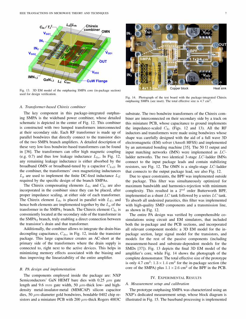
Fig. 13. 3D EM model of the outphasing SMPA core (in-package section)used for design verification.
A. Transformer-based Chireix combiner
The key component in this package-integrated outphas-ing SMPA is the wideband power combiner, whose detailedschematic is depicted in the center of Fig. 12. This combineris constructed with two lumped transformers interconnectedat their secondary side. Each RF transformer is made up ofparallel bondwires that directly connect to the transistor diesof the two SMPA branch amplifiers. A detailed description ofthese very low-loss bondwire-based transformers can be foundin [36]. The transformers can offer high magnetic coupling(e.g. 0.7) and thus low leakage inductance Lks. In Fig. 12,any remaining leakage inductance is either absorbed by thebroadband OMN or broadband-tuned by a capacitor Cks2. Inthe combiner, the transformers’ own magnetizing inductancesLp are used to implement the finite DC-feed inductance LErequired by the specific design of the branch SMPAs.
The Chireix compensating elements Lθc and Cθc are alsoincorporated in the combiner since they can be placed, afterproper impedance scaling, at either side of each transformer.The Chireix element Lθc is placed in parallel with LE , andhence both elements are implemented together by the Lp of thetransformer in the SMPA1 branch. The Chireix element Cθc isconveniently located at the secondary side of the transformer inthe SMPA2 branch, truly enabling a direct connection betweenthe transistor’s drain and that transformer.
Additionally, the combiner allows to integrate the drain-biasdecoupling capacitance, Cdec in Fig. 12, inside the transistorpackage. This large capacitance creates an AC-short at theprimary side of the transformers where the drain supply isconnected to, right next to the active devices. This helps inminimizing memory effects associated with the biasing andthus improving the linearizability of the entire amplifier.
B. PA design and implementation
The components employed inside the package are: NXPSemiconductors’ GaN HEMT bare dies with 0.25 µm gatelength and 9.6 mm gate width, 50 µm-thick low- and high-density metal-insulator-metal (MIMCAP) silicon capacitordies, 50 µm-diameter gold bondwires, bondable 0402 chip re-sistors and a miniature PCB with 200 µm-thick Rogers 4003C
IN1
IN2
VDD1
OUT
VDD2
VGG1
BPF
1.1x2.6 cm2
1.4x1.3 cm2
SMPA
Heat sinkCopper block
Fig. 14. Photograph of the test board with the package-integrated Chireixoutphasing SMPA (see inset). The total effective size is 4.7 cm2.
substrate. The two bondwire transformers of the Chireix com-biner are interconnected on their secondary side by a track onthis miniature PCB, whose capacitance to ground implementsthe impedance-scaled Cθc (Figs. 12 and 13). All the RFinductors and transformers were made using bondwires whoseshape was carefully designed with the aid of a full wave 3Delectromagnetic (EM) solver (Ansoft HFSS) and implementedby an automated bonding machine [35]. The 50 Ω output andinput matching networks (IMN) were implemented as LC-ladder networks. The two identical 3-stage LC-ladder IMNsconnect to the input package leads and contain stabilizingresistors, see Fig. 12. The OMN is a single-stage LC-ladderthat connects to the output package lead, see also Fig. 12.
Due to space constraints, the BPF was implemented outsidethe package. This filter was simultaneously optimized formaximum bandwidth and harmonics-rejection with minimumcomplexity. This resulted in a 2nd order Butterworth BPF,implemented as a shunt LC tank followed by a series LC tank.To absorb all undesired parasitics, this filter was implementedwith high-quality SMD components and a transmission line,as shown in Fig. 12.
The entire PA design was verified by comprehensible co-simulations using circuit and EM simulators, that includedboth the in-package and the PCB sections, and incorporatedall relevant component models: a 3D EM model for the in-package section, large signal model for the transistors, andmodels for the rest of the passive components (includingmeasurement-based and substrate-dependent models for theSMDs [37]). Fig. 13 depicts the final 3D EM model of theamplifier’s core, while Fig. 14 shows the photograph of thecomplete demonstrator. The total effective size of the prototypeis only 4.7 cm2: 1.3×1.4 cm2 for the in-package section (thecore of the SMPA) plus 1.1×2.6 cm2 of the BPF in the PCB.
IV. EXPERIMENTAL RESULTS
A. Measurement setup and calibration
The prototype outphasing SMPA was characterized using anNXP’s dedicated measurement setup, whose block diagram isillustrated in Fig. 15. The baseband processing is implemented

IEEE TRANSACTIONS ON MICROWAVE THEORY AND TECHNIQUES 8
IQ-Mixer
V2
0°90°
DA
DA
0°90°
DA
DA
V1
IA
IQ-Mixer
QA
IB
QB
Signal C
om
ponent Se
parator (S
.C.S
.)
Vout
-30dB
RF PowerMeter
Vector Signal
Analyzer
Digital Domain(Computer)
AWG
PA
Drivers
VG
As
Calibrated Reference Planes
Digital P
re-Distorter (D
.P.D
.)
Base
band Signal
(-20dB)
(-20dB)
-20dB
(-20dB)
Outphasing SMPA (DUT)
VD
D1,2
VG
G1,2
DC PowerSources &
Meters
x(t)
y(t)
z(t)
GPIBGPIB
GP
IB
GP
IB
LO
GP
IBControl & Measurements
Power combiner (for calibration only)
Fig. 15. NXP’s dedicated measurement setup for the outphasing SMPA demonstrator.
100
80
60
40
20
Frequency (GHz)
η DE
(%
)
49
47
45
43
41
Pea
k ou
tput
pow
er(d
Bm
)
2.10 2.15 2.20 2.25 2.30 2.35 2.40 2.45
0 dB
10 dB
6 dB
8 dB
100
80
60
40
20
Frequency (GHz)
η TO
T (
%)
49
47
45
43
41
Pea
k ou
tput
pow
er(d
Bm
)
2.10 2.15 2.20 2.25 2.30 2.35 2.40 2.45
0 dB
10 dB
6 dB
8 dB
(a)
100
80
60
40
20
Frequency (GHz)
η DE
(%
)
49
47
45
43
41
Pea
k ou
tput
pow
er(d
Bm
)
2.10 2.15 2.20 2.25 2.30 2.35 2.40 2.45
0 dB
10 dB
6 dB
8 dB
100
80
60
40
20
Frequency (GHz)
η TO
T (
%)
49
47
45
43
41
Pea
k ou
tput
pow
er(d
Bm
)
2.10 2.15 2.20 2.25 2.30 2.35 2.40 2.45
0 dB
10 dB
6 dB
8 dB
(b)
Fig. 16. Measured peak Pout and a) ηDE , b) ηTOT at different powerback-off levels (0 to 10 dB) as a function of frequency with VDD = 28 V.
in a PC where all the instruments are controlled and themeasured data is captured and processed. The baseband (andalso calibration) test signals are generated using a Tektronix’sAWG5014 arbitrary waveform generator and fed to two IQmodulators, follow by additional variable-gain (VGA) anddriver amplifiers. The output of the outphasing SMPA, ordevice under test (DUT), is fed to a R&S FSQ-26 signalanalyzer (with high speed baseband option B72) that down-
80
60
40
20
020 25 30 35 40 45 50
Output power (dBm)
η DE
(%)
@ 28V
20 25 30 35 40 45 50Output power (dBm)
η DE
(%)
2.20 GHz
2.25 GHz
2.30 GHz
@ 20V
80
60
40
20
0
2.20 GHz
2.25 GHz
2.30 GHz
(a)
80
60
40
20
020 25 30 35 40 45 50
Output power (dBm)
η DE
(%)
@ 28V
20 25 30 35 40 45 50Output power (dBm)
η DE
(%)
2.20 GHz
2.25 GHz
2.30 GHz
@ 20V
80
60
40
20
0
2.20 GHz
2.25 GHz
2.30 GHz
(b)
Fig. 17. Measured ηDE versus Pout across frequency at a) VDD = 20 Vand b) VDD = 28 V, between 2.2 and 2.3 GHz.
converts and samples the RF signal for digital predistortionand performs the linearity measurements. All RF inputs andoutput of the DUT are coupled to RF power meters in orderto compute its absolute power, efficiency and gain.
The entire setup is calibrated in two steps, for which a powercombiner (see Fig. 15) is connected instead of the actual DUT.First, each IQ mixer is independently calibrated digitally tocompensate for LO leakage and IQ phase and gain imbalance.

IEEE TRANSACTIONS ON MICROWAVE THEORY AND TECHNIQUES 9
Table IHIGHLIGHTS OF MEASURED EFFICIENCY AT 20 AND 28 V SUPPLY
DC supply Peak ηDE Back-off rangewith ηDE > 60%
20 V 81% @ 2.20 GHz 12.5 dB @ 2.25 GHz28 V 79% @ 2.20 GHz 8.1 dB @ 2.25 GHz
80
60
40
20
0-30 -25 -20 -15 -10 -5 0
Normalized output power (dB)
η DE
& η
TO
T (%
)
ηTOT GT
ηDE
GT
(dB
) &
PD
F (
x0.1
%)
32
28
24
20
16
12
8
4
0
1-carrier W-CDMA
Fig. 18. Measured total power gain (blue triangles), ηDE (black circles) andηTOT (black dots) as a function of back-off power at 2.30 GHz and VDD= 28 V. Also, the PDF of a single-carrier W-CDMA is shown.
In the second step, the two signal branches (i.e., IQ-mixer,VGA and pre-amplifier) are calibrated with respect to eachother in amplitude (AM) and phase (PM). Here, the two IQmixers deliver equal-amplitude but out-of-phase signals suchthat, after combination, will null each other (-60 dBc or better)in the absence of any imbalance. Digital compensation is usedfor this fine AM and PM adjustments. Once the measurementsetup is AM- and PM-calibrated, the outphasing SMPA isconnected and a finer calibration is performed to compensatefor the DUT’s own AM/PM imbalances.
B. Static characterization: single-tone
The outphasing SMPA demonstrator was first evaluated bysweeping a CW single-tone from 2.10 to 2.45 GHz. The GaNswitches were biased close to threshold (-2.3 V), and theirinput powers (Pin1,2) were fixed to 32 dBm. At each fre-quency, the outphasing angle was swept in order to modulatethe output power. The drain-efficiency (ηDE = Pout
PDC) was
calculated as the output power at the module’s 50 Ω connectorinterface (Pout) divided by the total DC power supplied tothe drains of the GaN transistors (PDC). The total-efficiency(ηTOT = Pout
PDC+Pdr) also included the total RF input power
delivered to the two inputs of the DUT (Pdr = Pin1 + Pin2).Fig. 16 shows the measured peak-output power, ηDE andηTOT versus frequency and output power back-off with anominal 28 V drain-supply. Excellent wideband performanceis observed from 2.1-2.4 GHz, with Pout= 47.9±0.6 dBm(peak at 48.5 dBm) and ηDE > 50% across >260 MHz, >160MHz and >80 MHz at 6, 8 and 10 dB back-off, respectively.
Measurements were also performed at 20 V drain-supply,and Fig. 17 shows and compares them with the nominal 28V supply. Note that at 20 V the efficiency performance isexcellent, but suffers a little at the desired 28 V due to practicalimplementation challenges encountered for this first prototype(e.g. deviations in some bondwire shapes). Table I highlights
Outphasing Transmitter
S.C
.S.
D.P
.D.
x(t) y(t)z(t)
SMPA
Fig. 19. Simplified block diagram for the single-input/single-output memo-ryless digital predistortion.
Normalized input x(t) amplitude0 0.2 0.4 0.6 0.8 1.0
1.0
0.8
0.6
0.4
0.2
0Nor
mal
ized
out
put y
(t)
ampl
itude
Normalized input x(t) amplitude
75
50
25
0
-25
Out
put-
inpu
t ph
ase
diffe
renc
e (d
eg)
0 0.2 0.4 0.6 0.8 1.0
AfterDPD
BeforeDPD
AfterDPD
BeforeDPD
(a)Normalized input x(t) amplitude
0 0.2 0.4 0.6 0.8 1.0
1.0
0.8
0.6
0.4
0.2
0Nor
mal
ized
out
put y
(t)
ampl
itude
Normalized input x(t) amplitude
75
50
25
0
-25
Out
put-
inpu
t ph
ase
diffe
renc
e (d
eg)
0 0.2 0.4 0.6 0.8 1.0
AfterDPD
BeforeDPD
AfterDPD
BeforeDPD
(b)
Fig. 20. Measured a) AM-AM and b) AM-PM response before (black) andafter (blue) memoryless DPD.
some of these results which demonstrate the high potential ofthe proposed amplifier. The highest peak power and best deepback-off efficiency was achieved at 2.3 GHz and the nominal28 V. For these conditions, Fig. 18 shows ηDE , ηTOT and thetotal power gain (GT = Pout
Pdr) as a function of back-off power.
GT peaks at 13.2 dB and reduces linearly with back-off powersince the driving power is constant.
C. Dynamic characterization: W-CDMA signal
The outphasing SMPA was characterized dynamically usingan uncompressed single-carrier 9.6 dB PAR W-CDMA signal,whose PDF is shown in Fig. 18. It was linearized usinga custom memoryless digital-predistortion (DPD). Fig. 19illustrates a simplified block diagram of the measurementsetup (Fig. 15) that is related to this DPD process. In Fig.19, z(t) and y(t) are the transmitter’s baseband input andoutput signals, respectively (i.e., before up- and after down-conversion by the signal analyzer), while x(t) is the originalW-CDMA signal. At first, y(t) is overcaptured without anyDPD (i.e., z(t) = x(t)) and averaged to reduce the system’snoise contribution. Next, y(t) and x(t) are time-aligned usinga circular correlation (for coarse alignment) followed by a
IEEE TRANSACTIONS ON MICROWAVE THEORY AND TECHNIQUES 10
Table IICOMPARISON STATE-OF-ART GAN RF PAS
W-CDMA P out,max ηDE,av ηTOT,av ACLR1,2 fo BW 6dB,60%** Reference
PAR (dB) (W) (%) (%) (dBc) (GHz) (MHz)9.6 70.6 53.5 43.8 -49, -56 2.30 > 100 This Work9.6 19 54.5 41.9 -47, -52 1.95 > 250 [12]7.7 >150 73.1#1 51.7#2 <-45, <-50 2.14 N.R. [10]9.6 90 50.5 ~47∗ -47, -51 2.14 N.R. [17]11.5 100 55.0 53.0∗ -51, -53 2.14 N.R. [6]
∗PAEav is given. #1Without and #2with (i.e. ηET,av) DC-DC modulator.∗∗BW 6dB,60% is the bandwidth at 6dB output back-off power with drain-efficiency larger than 60% (N.R. = not reported).
Before DPD
AfterDPD
Nor
mal
ized
Out
put P
ower
(dB
)
Offset frequency (MHz)-10 -5 0 5 10
10
0
-10
-20
-30
-40
-50
-60
-70
Fig. 21. Measured spectrum with a 9.6 dB PAR W-CDMA before (black)and after (blue) memoryless DPD.
2.55 MHz/Center 2.3 GHz Span 25.5 MHz
RBW 30 kHzVBW 300 kHzSWT 100 msRef 20 dBm Att 15 dB
Adjacent ChannelBandwidthSpacing
Alternate ChannelBandwidthSpacing
3.84 MHz5 MHz
3.84 MHz10 MHz
LowerUpper
LowerUpper
-49.53 dB-54.78 dB
-56.54 dB-61.83 dB
Fig. 22. Measured ACLR1,2 with a 9.6 dB PAR W-CDMA after DPD.
linear subsample sweep (for fine alignment). A multiple-segment low-order polynomial AM-AM and AM-PM fittingprocess is used to model the inverse PA characteristics. Itusually requires 5-7 segments of 3rd or 4th order polynomials.This approach can accurately model the detailed PA’s inversecharacteristics without overfitting which would occur with asingle-segment high-order curve fit. Then, the DPD predistortsx(t) and generates z(t), which finally leads to an improvedy(t). This memoryless DPD was developed and optimized foroutphasing amplifiers and provides optimum linearisation evenwhen benchmarked against Volterra solutions.
Since this DPD is single-input/single-output, it is in factlinearizing the entire transmitter, i.e. including the (baseband)signal-component-separator. In principle, the SCS generatesthe signals of the two branches with a differential phasethat is ideally an arc-sine function of the amplitude of theoriginal signal (i.e. ±θ(t) = sin−1 |E(t)| in Fig. 2). However,
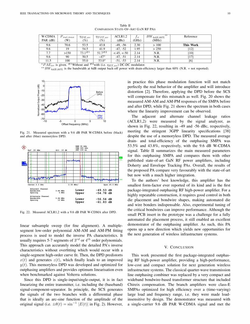
in practice this phase modulation function will not matchperfectly the real behavior of the amplifier and will introducedistortion [2]. Therefore, applying the DPD before the SCSwill compensate for this mismatch as well. Fig. 20 shows themeasured AM-AM and AM-PM responses of the SMPA beforeand after DPD, while Fig. 21 shows the spectrum in both caseswhere the linearity improvement can be observed.
The adjacent and alternate channel leakage ratios(ACLR1,2) were measured by the signal analyzer, asshown in Fig. 22, resulting in -49 and -56 dBc, respectively,meeting the stringent 3GPP linearity specifications [38]despite the use of a memoryless DPD. The measured averagedrain- and total-efficiency of the outphasing SMPA was53.5% and 43.8%, respectively, with the 9.6 dB W-CDMAsignal. Table II summarizes the main measured parametersfor this outphasing SMPA and compares them with otherpublished state-of-art GaN RF power amplifiers, includingDoherty and Envelope Tracking PAs. Overall, the results ofthe proposed PA compare very favourably with the state-of-artbut now with a much higher integration.
To the authors’ best knowledge, this amplifier has thesmallest form-factor ever reported of its kind and is the firstpackage-integrated outphasing RF high-power amplifier. For ahighly repeatable construction, it requires good control in bothdie placement and bondwire shapes, making automated dieand wire bonders indispensable. Also, experimental tuning ofthe critical bondwires can improve performance. Although thesmall PCB insert in the prototype was a challenge for a fullyautomated die placement process, it still enabled an excellentdemonstrator of the outphasing amplifier. As such, this PAopens up a new direction which yields new opportunities forthe next generation of wireless infrastructure systems.
V. CONCLUSION
This work presented the first package-integrated outphas-ing RF high-power amplifier, providing a high-performance,low-cost and compact solution for next generation wirelessinfrastructure systems. The classical quarter-wave transmissionline outphasing combiner was replaced by a very compact andwideband bondwire-based transformer structure that includedChireix compensation. The branch amplifiers were class-ESMPAs optimized for high efficiency over a (time-varying)large load and frequency range, i.e. they were made load-insensitive by design. The demonstrator was measured witha single-carrier 9.6 dB PAR W-CDMA signal and met the

IEEE TRANSACTIONS ON MICROWAVE THEORY AND TECHNIQUES 11
stringent 3GPP linearity requirements with a memoryless dig-ital predistortion. It achieved state-of-art performance withinthe smallest form-factor ever reported. In addition, this workprovided deeper insight on the design of the branch amplifiersfor outphasing transmitters and an explicit recognition of theinteraction between the net power factor of the combiner(used by previous works to solely quantify efficiency) and thespecific amplifier class. Such interaction ultimately determinesthe overall efficiency performance of the transmitter.
ACKNOWLEDGMENT
The authors would like to thank Antoine van Dijk andthe Nijmegen prototyping team (for prototype assembly), RobHeeres (for MIMCAP design) and Rik Jos (for supportingand guiding these research activities) all from NXP Semi-conductors. Thomas Roedle (NXP Semiconductors) and allparticipants from Fraunhofer IAF that contributed to NXP’s0.25 µm GaN technology are acknowledged. Koen Buismanand Rui Hou, from TU Delft, are acknowledged for providinguseful support and comments on the manuscript. Modelithics,Inc., Tampa, FL. is acknowledged for providing ModelithicsCLR models, utilized under the University License Program.This work has been supported by the PANAMA and theHEECS european projects. Additionally, the first author wouldlike thank the support from the Mexican National Council forScience and Technology (scholar 206449).
REFERENCES
[1] F. H. Raab, P. M. Asbeck, S. C. Cripps, P. B. Kenington, Z. B. Popovic,N. Pothecary, J. F. Sevic, and N. O. Sokal, “Power amplifiers andtransmitters for RF and microwave,” IEEE Trans. Microw. Theory Tech.,vol. 50, no. 3, pp. 814–826, Mar. 2002.
[2] S. C. Cripps, RF Power Amplifiers for Wireless Communications, 2nd ed.Artech House, Jun. 2006, ch. 10.
[3] H. Chireix, “High power outphasing modulation,” Proc. of the Instituteof Radio Engineers, vol. 23, no. 11, pp. 1370–1392, Nov. 1935.
[4] F. H. Raab, “Efficiency of outphasing RF power-amplifier systems,”IEEE Trans. Commun., vol. 33, no. 10, pp. 1094–1099, Oct. 1985.
[5] W. H. Doherty, “A new high efficiency power amplifier for modulatedwaves,” Proc. of the Institute of Radio Engineers, vol. 24, no. 9, pp.1163–1182, Sep. 1936.
[6] M. J. Pelk, W. C. Neo, J. R. Gajadharsing, R. S. Pengelly, andL. C. N. de Vreede, “A high-efficiency 100-W GaN three-way Dohertyamplifier for base-station applications,” IEEE Trans. Microw. TheoryTech., vol. 56, no. 7, pp. 1582–1591, Jul. 2008.
[7] J. H. Qureshi, N. Li, W. C. E. Neo, F. van Rijs, I. Blednov, and L. C. N.de Vreede, “A wide-band 20W LMOS Doherty power amplifier,” inIEEE MTT-S Int. Microwave Symp. Dig., May 2010, pp. 1504–1507.
[8] D. Gustafsson, C. M. Andersson, and C. Fager, “A modified Dohertypower amplifier with extended bandwidth and reconfigurable efficiency,”IEEE Trans. Microw. Theory Tech., vol. 61, no. 1, pp. 533–542, Jan.2013.
[9] D. F. Kimball, J. Jeong, C. Hsia, P. Draxler, S. Lanfranco, W. Nagy,K. Linthicum, L. E. Larson, and P. M. Asbeck, “High-efficiencyenvelope-tracking W-CDMA base-station amplifier using GaN HFETs,”IEEE Trans. Microw. Theory Tech., vol. 54, no. 11, pp. 3848–3856, Nov.2006.
[10] J. Jeong, D. F. Kimball, M. Kwak, C. Hsia, P. Draxler, and P. M. Asbeck,“Modeling and design of RF amplifiers for envelope tracking WCDMAbase-station applications,” IEEE Trans. Microw. Theory Tech., vol. 57,no. 9, pp. 2148–2159, Sep. 2009.
[11] C. Hsia, A. Zhu, J. J. Yan, P. Draxler, D. F. Kimball, S. Lanfranco, andP. M. Asbeck, “Digitally assisted dual-switch high-efficiency envelopeamplifier for envelope-tracking base-station power amplifiers,” IEEETrans. Microw. Theory Tech., vol. 59, no. 11, pp. 2943–2952, Nov. 2011.
[12] M. P. van der Heijden, M. Acar, J. S. Vromans, and D. A. Calvillo-Cortes, “A 19W high-efficiency wide-band CMOS-GaN class-E ChireixRF outphasing power amplifier,” in IEEE MTT-S Int. Microwave Symp.Dig., Jun. 2011, pp. 1–4.
[13] W. Tai, H. Xu, A. Ravi, H. Lakdawala, O. Bochobza-Degani, L. R.Carley, and Y. Palaskas, “A transformer-combined 31.5 dBm outphasingpower amplifier in 45 nm LP CMOS with dynamic power control forback-off power efficiency enhancement,” IEEE J. Solid-State Circuits,vol. 47, no. 7, pp. 1646–1658, Jul. 2012.
[14] P. Madoglio, A. Ravi, H. Xu, K. Chandrashekar, M. Verhelst, S. Peller-ano, L. Cuellar, M. Aguirre, M. Sajadieh, O. Degani, H. Lakdawala,and Y. Palaskas, “A 20dBm 2.4GHz digital outphasing transmitter forWLAN application in 32nm CMOS,” in IEEE Int. Solid-State CircuitsConf. Dig. of Tech. Papers, Feb. 2012, pp. 168–170.
[15] D. Cox, “Linear amplification with nonlinear components,” IEEE Trans.Commun., vol. 22, no. 12, pp. 1942–1945, Dec. 1974.
[16] R. Beltran, F. H. Raab, and A. Velazquez, “HF outphasing transmitterusing class-E power amplifiers,” in IEEE MTT-S Int. Microwave Symp.Dig., Jun. 2009, pp. 757–760.
[17] J. H. Qureshi, M. J. Pelk, M. Marchetti, W. C. E. Neo, J. R. Ga-jadharsing, M. P. van der Heijden, and L. C. N. de Vreede, “A 90-W peak power GaN outphasing amplifier with optimum input signalconditioning,” IEEE Trans. Microw. Theory Tech., vol. 57, no. 8, pp.1925–1935, Aug. 2009.
[18] W. Gerhard and R. Knoechel, “Novel transmission line combiner forhighly efficient outphasing RF power amplifiers,” in European Mi-crowave Conf. Proc., Oct. 2007, pp. 1433 –1436.
[19] I. Hakala, D. K. Choi, L. Gharavi, N. Kajakine, J. Koskela, andR. Kaunisto, “A 2.14-GHz Chireix outphasing transmitter,” IEEE Trans.Microw. Theory Tech., vol. 53, no. 6, pp. 2129–2138, Jun. 2005.
[20] M. C. A. van Schie, M. P. van der Heijden, M. Acar, A. J. M.de Graauw, and L. C. N. de Vreede, “Analysis and design of a widebandhigh efficiency CMOS outphasing amplifier,” in IEEE Radio FrequencyIntegrated Circuits Symp., May 2010, pp. 399–402.
[21] N. Singhal, H. Zhang, and S. Pamarti, “A zero-voltage-switchingcontour-based outphasing power amplifier,” IEEE Trans. Microw. TheoryTech., vol. 60, no. 6, pp. 1896–1906, Jun. 2012.
[22] D. A. Calvillo-Cortes, M. P. van der Heijden, and L. C. N. de Vreede,“A 70W package-integrated class-E Chireix outphasing RF power am-plifier,” in IEEE MTT-S Int. Microwave Symp. Dig., Jun. 2013.
[23] P. A. Godoy, S. Chung, T. W. Barton, D. J. Perreault, and J. L. Dawson,“A highly efficient 1.95-GHz, 18-W asymmetric multilevel outphasingtransmitter for wideband applications,” in IEEE MTT-S Int. MicrowaveSymp. Dig., Jun. 2011, pp. 1–4.
[24] D. J. Perreault, “A new power combining and outphasing modulationsystem for high-efficiency power amplification,” IEEE Trans. Circuitsand Syst. I, Reg. Papers, vol. 58, no. 8, pp. 1713–1726, Aug. 2011.
[25] T. W. Barton, J. L. Dawson, and D. J. Perreault, “Experimental validationof a four-way outphasing combiner for microwave power amplification,”IEEE Microw. and Wireless Compon. Lett., vol. 23, no. 1, pp. 28–30,Jan. 2013.
[26] D. A. Calvillo-Cortes, L. C. N. de Vreede, and M. de Langen, “A com-pact and power-scalable 70W GaN class-E power amplifier operatingfrom 1.7 to 2.6 GHz,” in Asia-Pacific Microwave Conf. Proc., Dec.2011, pp. 1546 –1549.
[27] K. Shi, D. A. Calvillo-Cortes, L. C. N. de Vreede, and F. van Rijs,“A compact 65W 1.7-2.3GHz class-E GaN power amplifier for basestations,” in European Microwave Conf. Proc., Oct. 2011, pp. 1103–1106.
[28] R. Zhang, M. Acar, M. P. van der Heijden, M. Apostolidou, L. C. N.de Vreede, and D. M. W. Leenaerts, “A 550-1050MHz +30dBm class-Epower amplifier in 65nm CMOS,” in IEEE Radio Frequency IntegratedCircuits Symp., Jun. 2011, pp. 1–4.
[29] N. O. Sokal and A. D. Sokal, “Class E - A new class of high-efficiencytuned single-ended switching power amplifiers,” Solid-State Circuits,IEEE Journal of, vol. 10, no. 3, pp. 168–176, Jun. 1975.
[30] F. H. Raab, “Idealized operation of the class E tuned power amplifier,”IEEE Trans. Circuits and Syst., vol. 24, no. 12, pp. 725–735, Dec. 1977.
[31] M. Acar, A. J. Annema, and B. Nauta, “Variable-voltage class-E poweramplifiers,” in IEEE MTT-S Int. Microwave Symp. Dig., Jun. 2007, pp.1095–1098.
[32] ——, “Generalized analytical design equations for variable slope class-E power amplifiers,” in 13th IEEE Int. Conf. on Electronics, Circuitsand Systems, Dec. 2006, pp. 431–434.
[33] ——, “Analytical design equations for class-E power amplifiers,” IEEETrans. Circuits and Syst. I, Reg. Papers, vol. 54, no. 12, pp. 2706–2717,Dec. 2007.

IEEE TRANSACTIONS ON MICROWAVE THEORY AND TECHNIQUES 12
[34] A. Grebennikov and H. Jaeger, “Class E with parallel circuit - A newchallenge for high-efficiency RF and microwave power amplifiers,” inIEEE MTT-S Int. Microwave Symp. Dig., Jun. 2002, pp. 1627–1630.
[35] D. A. Calvillo-Cortes, K. Shi, M. de Langen, F. van Rijs, and L. C. N.de Vreede, “On the design of package-integrated RF high-power ampli-fiers,” in IEEE MTT-S Int. Microwave Symp. Dig., Jun. 2012, pp. 1–3.
[36] D. A. Calvillo-Cortes, L. C. N. de Vreede, and M. P. van der Heijden, “Atransformer for high-power RF applications using bondwires in parallel,”in European Microwave Conf. Proc., Oct. 2011, pp. 103–106.
[37] Passive component library CLRTM (v8.2). Modelithics, Inc. [Online].Available: www.modelithics.com
[38] Base station conformance testing (FDD), 3rd Generation PartnershipProject, technical specification, 3GPP TS 25.141 (V11.3.0), Sep. 2012.
David A. Calvillo-Cortes (S’03) was born inGuadalajara, Mexico, in 1982. He received the B.Sc.degree (best student award) in communications andelectronics engineering from the Universidad deGuadalajara, Guadalajara, Mexico, in 2005, and theM.Sc. degree (cum laude) in electrical engineeringfrom the Delft University of Technology, Delft,The Netherlands, in 2009. From 2005 to 2007he worked for Continental Automotive (formerlySiemens-VDO) as hardware development engineer.In 2008-2009, he worked on high-voltage/-power
CMOS drivers for RF SMPAs at the Integrated RF Solutions Research Groupin NXP Semiconductors, Eindhoven, The Netherlands. In late 2009, he joinedthe Electronics Research Laboratory at Delft University of Technology wherehe is currently working toward the Ph.D. degree in electrical engineering.
Mark P. van der Heijden (S’00-M’05) was born inBenthuizen, The Netherlands, in 1976. He receivedthe B.Sc. degree in electrical engineering from theHaagse Hogeschool, The Hague, The Netherlands,in 1998, the PDEng and Ph.D. degrees in electricalengineering from the Delft University of Technol-ogy, Delft, The Netherlands, in 2000 and 2005,respectively. From 1998 to 2004, he was with theLaboratory of Electronic Components, Technology& Materials, in the faculty of Electrical Engineeringat Delft University of Technology, where he worked
on RF amplifier design techniques for linearity and dynamic range. In 2004,he joined the research department of NXP Semiconductors (formerly PhilipsSemiconductors) as a senior scientist. In 2010, he joined the R&D departmentof the Business Line High Performance RF. His research and developmentinterests include high-efficiency RF power amplifier design and advancedtransmitter architectures for wireless infrastructure. Currently he is involved ina digital transmitter architecture that is built around a switch-mode outphasingpower amplifier for base stations.
Mustafa Acar was born in Gaziantep,Turkey, in1979. He received the B.S. degree (with honors)from Middle East Technical University, Ankara,Turkey, in 2001, the M.S degree (high honor, cumlaude), in 2003 and the Ph.D. degree, in 2011 fromthe Integrated Circuit (IC) Design Group, Universityof Twente, Enschede, The Netherlands. During 2003,he worked on high-speed low-power frequency di-viders in sub-micrometer CMOS technologies for hismaster thesis at the Integrated Transceivers Group,Natlab, Philips Research Laboratories, Eindhoven,
The Netherlands. From 2003 to 2007, he worked on his doctoral researchproject on CMOS PAs. Since 2007, he has been with the RF Advanced DesignGroup of NXP Semiconductors, Eindhoven, The Netherlands. His currentresearch interests are on high efficiency power amplifiers for base stations.Mr. Acar was the recipient of the Philips Funding for Microelectronics MasterProgram at the University of Twente.
Michel T. W. de Langen was born in Amsterdam,The Netherlands, in 1962. He received a M.Sc.degree in physics from the University Twente, En-schede, The Netherlands, in 1986. From 1987 to1993 he was with Philips Applied Technologies, in-volved in research on electronic assembly processes.From 1994 onwards he joined NXP Semiconductors(formerly Philip Semiconductors) in Nijmegen, TheNetherlands. He was responsible for the introductionof new package concepts like BGA, Multi ChipModules and CMOS imaging packages. Currently
he is working on assembly and package research for RF power devices.
Robin Wesson was born in Rugby, United Kingdom,in 1973. He was granted a first class degree inPhysics and Electronic Engineering from Loughbor-ough University of Technology in 1996. He is asystem architect for NXP RF power in Nijmegen,The Netherlands. He has 17 years of industrialRF system, circuit and product design experience,with Motorola, Sagentia, IP Wireless & Axis NTamong others. He is currently working on signalprocessing and linearisation techniques for switch-mode outphasing power amplifier systems.
Fred van Rijs received the Ph.D. degree in electricalengineering (cum laude) from Delft University ofTechnology, Delft, The Netherlands, in 1992. In1992, he joined Philips Research Laboratories, Eind-hoven, The Netherlands, where he was involved withadvanced silicon technologies and demonstrated suc-cessfully silicon double-poly bipolar technology forpower amplifiers for cellular showing record-levelpower-added efficiency. In 1999, he joined PhilipsSemiconductors, Nijmegen, The Netherlands, wherehe was with the Innovation Group for three years
working on CATV initiating pHEMT technology for the next generationof CATV power amplifiers. After that, for three and a half years, he wasinvolved with power transistors for base stations and was responsible for thedevelopment of LDMOS technology. In 2005, he joined the Innovation CenterRF, where he is currently involved with low-distortion GaAs–AlGaAs HFETsand GaN. He has authored or coauthored over 20 technical papers.
Leo C. N. de Vreede (M’01-SM’04) was born inDelft, The Netherlands, in 1965. He received theB.S. degree (cum laude) in electrical engineeringfrom the Hague Polytechnic in 1988. He received thePh.D. degree (cum laude) from Delft University ofTechnology (TU Delft) in 1996. In 1988, he joinedthe Laboratory of Telecommunication and RemoteSensing Technology at TU Delft. He worked onthe characterization and physical modeling of CMCcapacitors (1988-1990), on modeling and designaspects of HF silicon IC’s for wideband communica-
tion systems (1990-1996), and on the nonlinear distortion behavior of bipolartransistors at DIMES, TU Delft, when he was appointed assistant professorin 1996. In the winter season of ’98-’99, he was a guest of the high speeddevice group at the University of San Diego, California. In 1999, he becameassociate professor, responsible for the Microwave Components Group, at TUDelft. Since that time he has worked on RF solutions for improved linearityand RF performance at the device, circuit and system level. He is co-founder/ advisor of Anteverta-mw, (co)recipient of the IEEE Microwave prize in2008, mentor of the Else Kooi prize awarded Ph.D. work in 2010, mentor ofthe Dow Energy dissertation prize awarded Ph.D. work in 2011, (co)authoredmore than 100 IEEE refereed conference and journal papers and holds severalpatents. His current interest includes RF measurement systems, technologyoptimization and circuit concepts for wireless systems.