Embed Size (px)
Citation preview
1
Semiconductor Optical Sources
2
Source Characteristics
• Important Parameters
– Electrical-optical conversion efficiency
– Optical power
– Wavelength
– Wavelength distribution (called linewidth)
– Cost
• Semiconductor lasers
– Compact
– Good electrical-optical conversion efficiency
– Low voltages
– Los cost
3
Semiconductor Optoelectronics
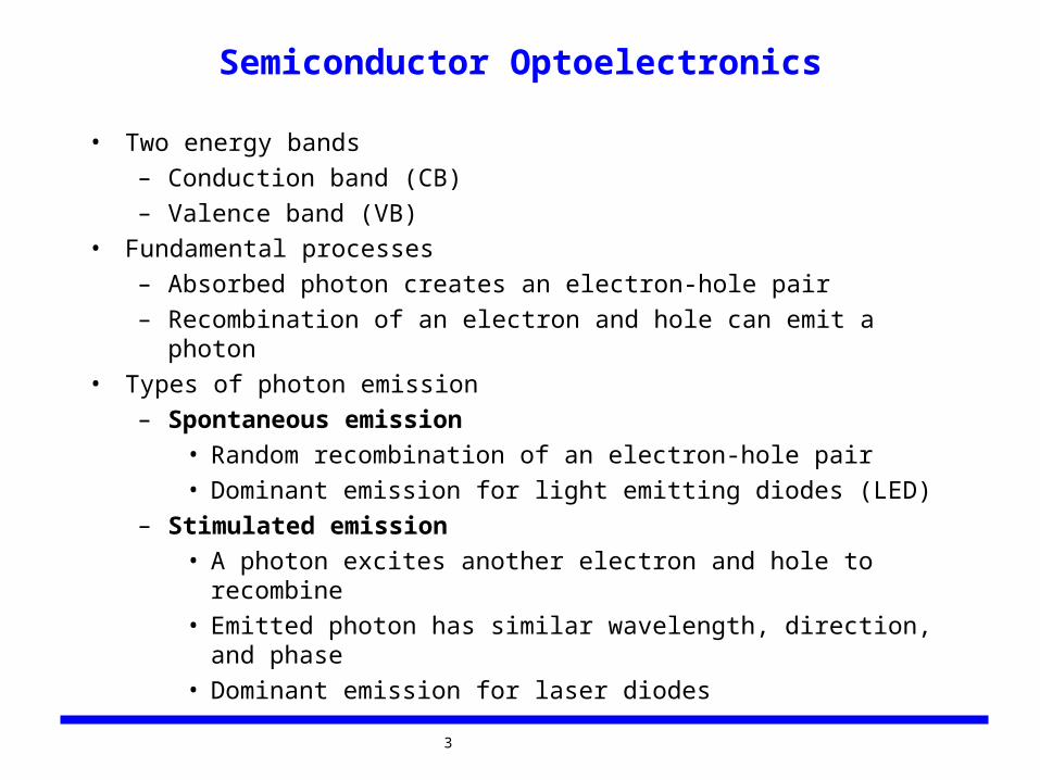
• Two energy bands
– Conduction band (CB)
– Valence band (VB)
• Fundamental processes
– Absorbed photon creates an electron-hole pair
– Recombination of an electron and hole can emit a photon
• Types of photon emission
– Spontaneous emission
• Random recombination of an electron-hole pair
• Dominant emission for light emitting diodes (LED)
– Stimulated emission
• A photon excites another electron and hole to recombine
• Emitted photon has similar wavelength, direction, and phase
• Dominant emission for laser diodes
4
Basic Light Emission Processes
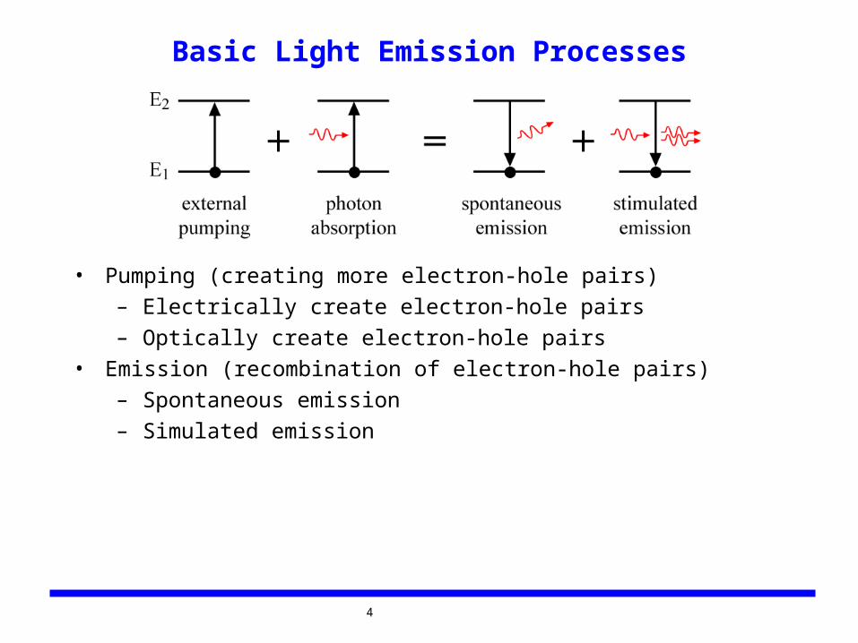
• Pumping (creating more electron-hole pairs)
– Electrically create electron-hole pairs
– Optically create electron-hole pairs
• Emission (recombination of electron-hole pairs)
– Spontaneous emission
– Simulated emission
5
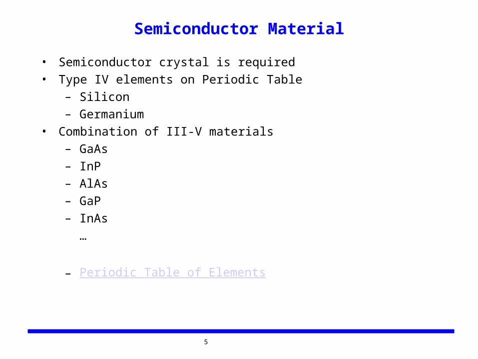
Semiconductor Material
• Semiconductor crystal is required
• Type IV elements on Periodic Table
– Silicon
– Germanium
• Combination of III-V materials
– GaAs
– InP
– AlAs
– GaP
– InAs
…
– Periodic Table of Elements
6
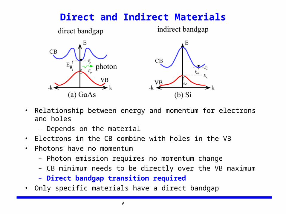
Direct and Indirect Materials
• Relationship between energy and momentum for electrons and holes
– Depends on the material
• Electrons in the CB combine with holes in the VB
• Photons have no momentum
– Photon emission requires no momentum change
– CB minimum needs to be directly over the VB maximum
– Direct bandgap transition required
• Only specific materials have a direct bandgap
7
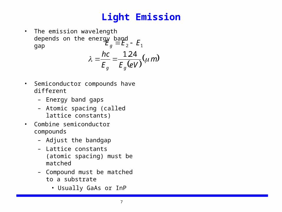
Light Emission• The emission wavelength depends on
the energy band gap
• Semiconductor compounds have different
– Energy band gaps
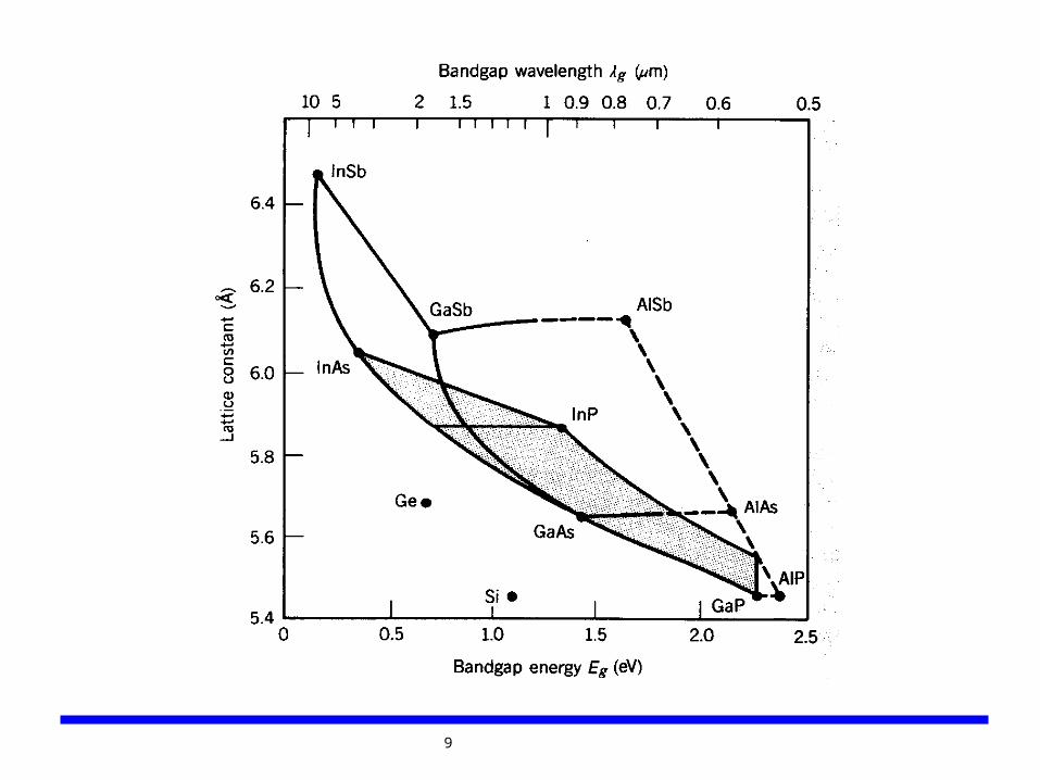
– Atomic spacing (called lattice constants)
• Combine semiconductor compounds
– Adjust the bandgap
– Lattice constants (atomic spacing) must be matched
– Compound must be matched to a substrate
• Usually GaAs or InP
12 EEEg
meVEE
hc
gg
24.1
8
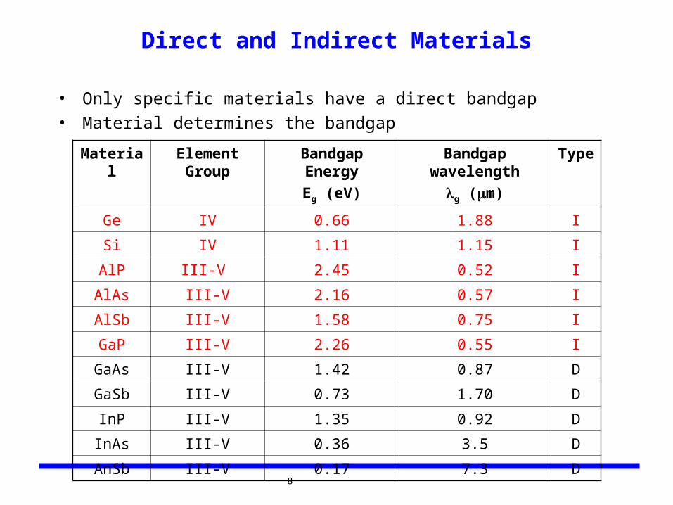
Direct and Indirect Materials
• Only specific materials have a direct bandgap
• Material determines the bandgap
Material Element Group Bandgap Energy
Eg (eV)
Bandgap wavelength
g (m)
Type
Ge IV 0.66 1.88 I
Si IV 1.11 1.15 I
AlP III-V 2.45 0.52 I
AlAs III-V 2.16 0.57 I
AlSb III-V 1.58 0.75 I
GaP III-V 2.26 0.55 I
GaAs III-V 1.42 0.87 D
GaSb III-V 0.73 1.70 D
InP III-V 1.35 0.92 D
InAs III-V 0.36 3.5 D
AnSb III-V 0.17 7.3 D
9
10
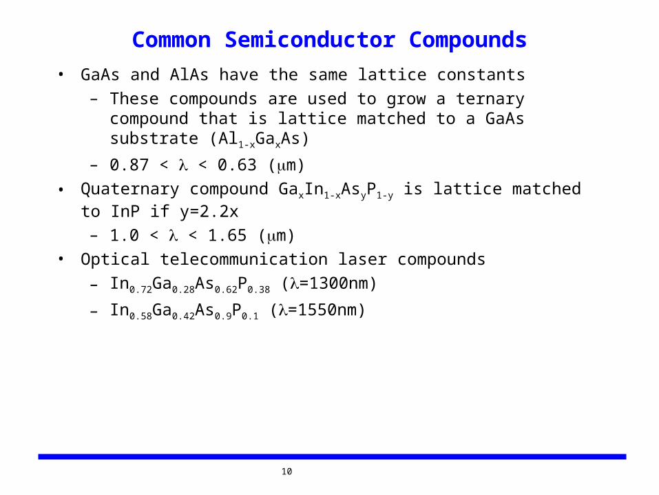
Common Semiconductor Compounds
• GaAs and AlAs have the same lattice constants
– These compounds are used to grow a ternary compound that is lattice matched to a GaAs substrate (Al1-xGaxAs)
– 0.87 < < 0.63 (m)
• Quaternary compound GaxIn1-xAsyP1-y is lattice matched to InP if y=2.2x
– 1.0 < < 1.65 (m)
• Optical telecommunication laser compounds
– In0.72Ga0.28As0.62P0.38 (=1300nm)
– In0.58Ga0.42As0.9P0.1 (=1550nm)
11
Optical Sources
• Two main types of optical sources
– Light emitting diode (LED)
• Large wavelength content
• Incoherent
• Limited directionality
– Laser diode (LD)
• Small wavelength content
• Highly coherent
• Directional
12
Light Emitting Diodes (LED)
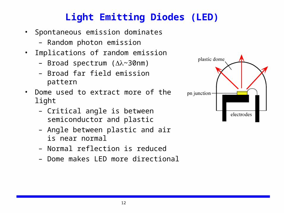
• Spontaneous emission dominates
– Random photon emission
• Implications of random emission
– Broad spectrum (~30nm)
– Broad far field emission pattern
• Dome used to extract more of the light
– Critical angle is between semiconductor and plastic
– Angle between plastic and air is near normal
– Normal reflection is reduced
– Dome makes LED more directional
13
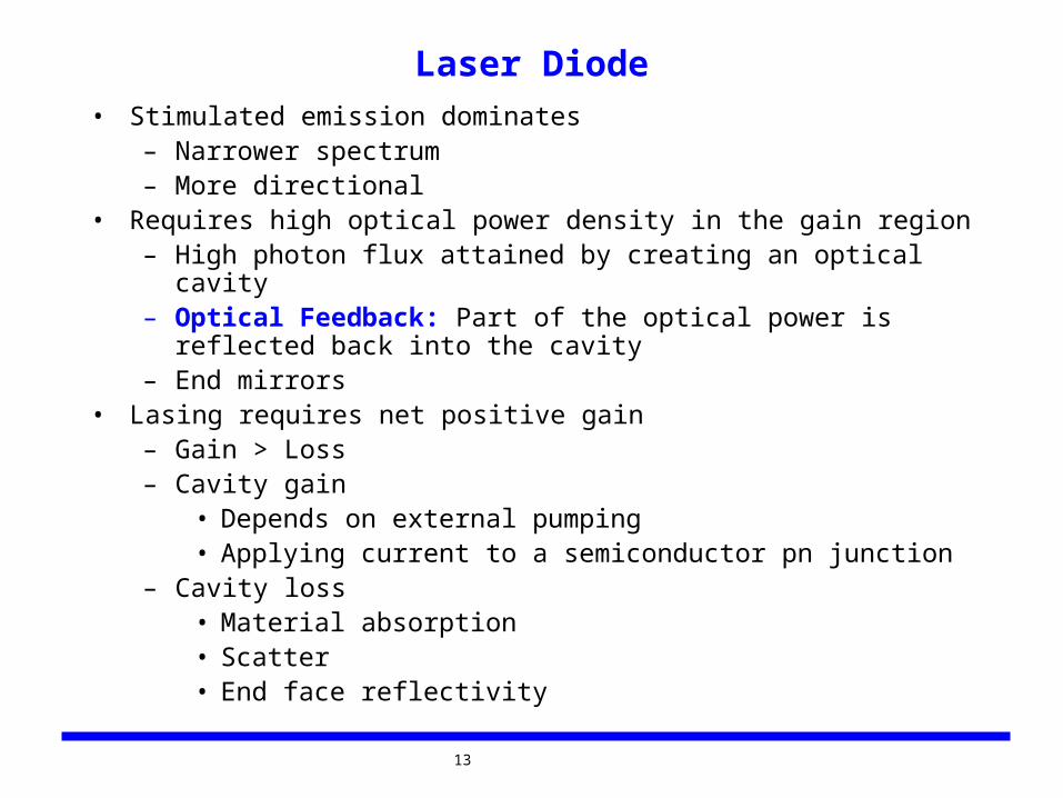
Laser Diode• Stimulated emission dominates
– Narrower spectrum– More directional
• Requires high optical power density in the gain region– High photon flux attained by creating an optical cavity– Optical Feedback: Part of the optical power is reflected back into the
cavity– End mirrors
• Lasing requires net positive gain– Gain > Loss– Cavity gain
• Depends on external pumping• Applying current to a semiconductor pn junction
– Cavity loss• Material absorption• Scatter• End face reflectivity
14
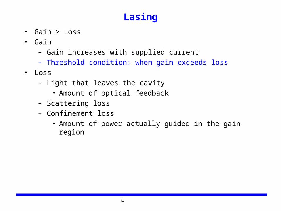
Lasing
• Gain > Loss
• Gain
– Gain increases with supplied current
– Threshold condition: when gain exceeds loss
• Loss
– Light that leaves the cavity
• Amount of optical feedback
– Scattering loss
– Confinement loss
• Amount of power actually guided in the gain region
15
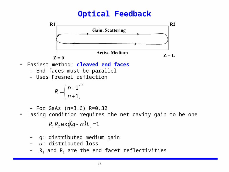
Optical Feedback
• Easiest method: cleaved end faces– End faces must be parallel– Uses Fresnel reflection
– For GaAs (n=3.6) R=0.32• Lasing condition requires the net cavity gain to be one
– g: distributed medium gain– : distributed loss– R1 and R2 are the end facet reflectivities
1exp21 LgRR
2
1
1
n
nR
16
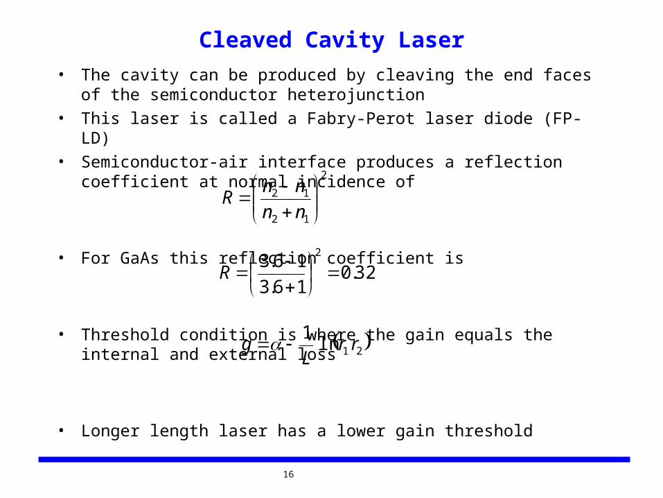
Cleaved Cavity Laser
• The cavity can be produced by cleaving the end faces of the semiconductor heterojunction
• This laser is called a Fabry-Perot laser diode (FP-LD)
• Semiconductor-air interface produces a reflection coefficient at normal incidence of
• For GaAs this reflection coefficient is
• Threshold condition is where the gain equals the internal and external loss
• Longer length laser has a lower gain threshold
2
12
12
nn
nnR
32.016.3
16.32
R
21ln1
rrL
g
17
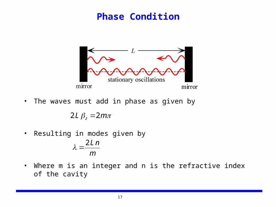
Phase Condition
• The waves must add in phase as given by
• Resulting in modes given by
• Where m is an integer and n is the refractive index of the cavity
mL z 22
m
nL2
18
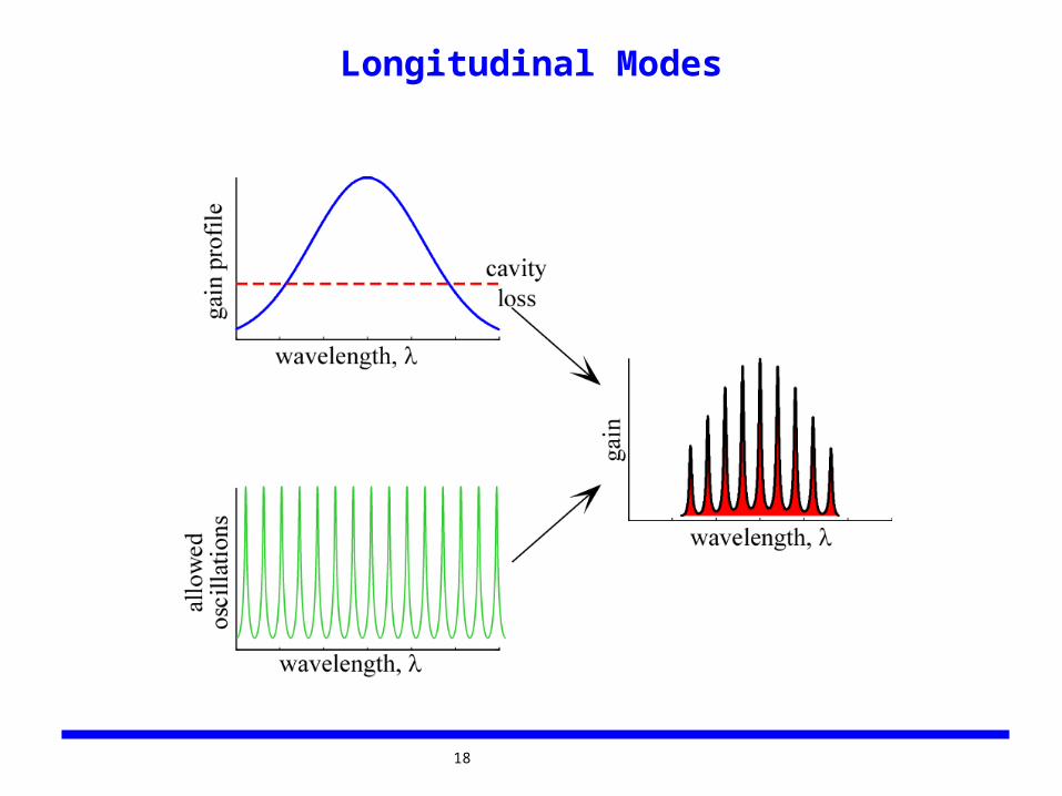
Longitudinal Modes
19
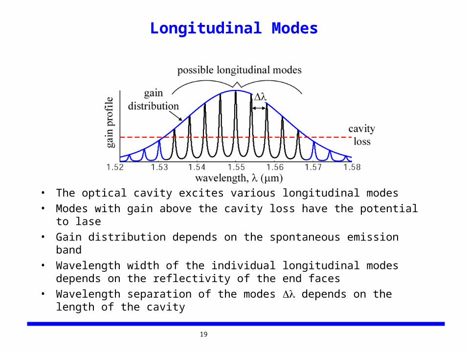
Longitudinal Modes
• The optical cavity excites various longitudinal modes
• Modes with gain above the cavity loss have the potential to lase
• Gain distribution depends on the spontaneous emission band
• Wavelength width of the individual longitudinal modes depends on the reflectivity of the end faces
• Wavelength separation of the modes depends on the length of the cavity
20
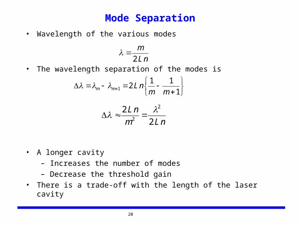
Mode Separation
• Wavelength of the various modes
• The wavelength separation of the modes is
• A longer cavity
– Increases the number of modes
– Decrease the threshold gain
• There is a trade-off with the length of the laser cavity
nL
m
2
1
1121 mm
nLmm
nLm
nL
2
2 2
2
21
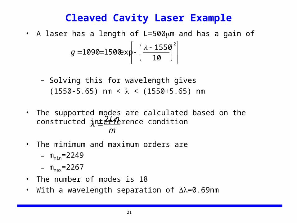
Cleaved Cavity Laser Example
• A laser has a length of L=500m and has a gain of
– Solving this for wavelength gives
(1550-5.65) nm < < (1550+5.65) nm
• The supported modes are calculated based on the constructed interference condition
• The minimum and maximum orders are
– mmin=2249
– mmax=2267
• The number of modes is 18
• With a wavelength separation of =0.69nm
2
10
1550exp15001090
g
m
nL2
22
Single Longitudinal Mode Lasers
• Multimode laser have a large wavelength content
• A large wavelength content decrease the performance of the optical link
• Methods used to produce single longitudinal mode lasers
– Cleaved-coupled-cavity (C3) laser
– Distributed feedback laser (DFB) laser
23
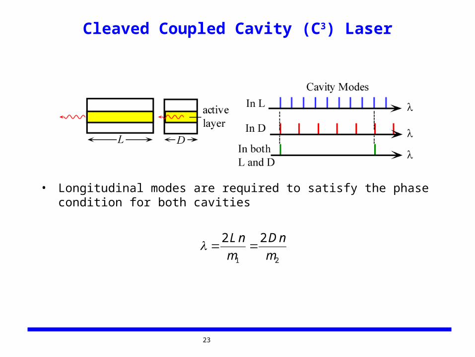
Cleaved Coupled Cavity (C3) Laser
• Longitudinal modes are required to satisfy the phase condition for both cavities
21
22
m
nD
m
nL
24
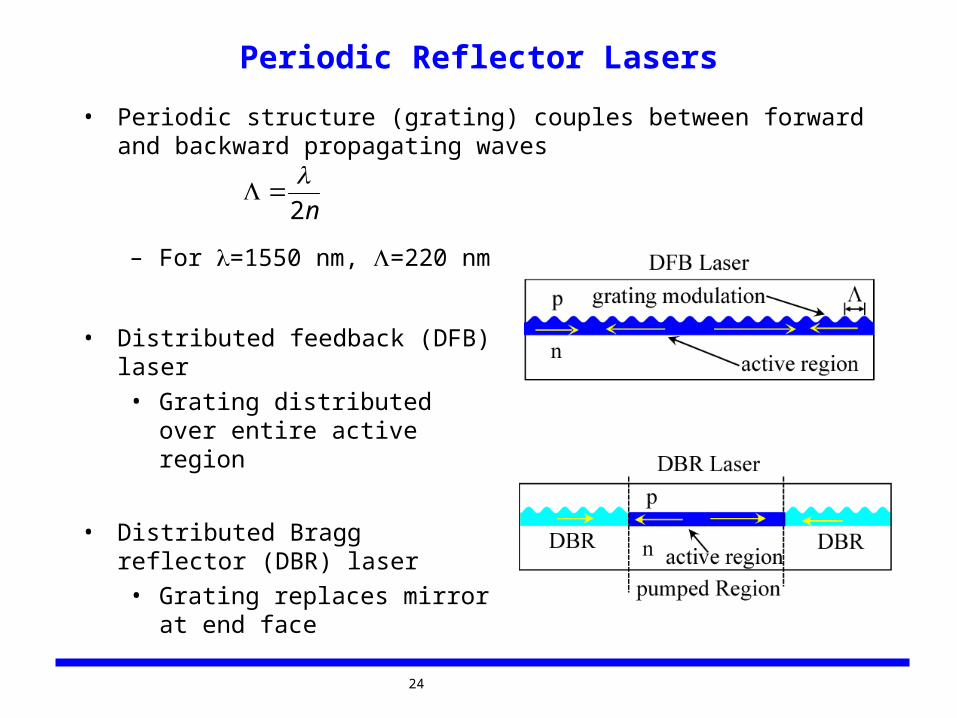
Periodic Reflector Lasers
• Periodic structure (grating) couples between forward and backward propagating waves
– For =1550 nm, =220 nm
n2
• Distributed feedback (DFB) laser
• Grating distributed over entire active region
• Distributed Bragg reflector (DBR) laser
• Grating replaces mirror at end face
25
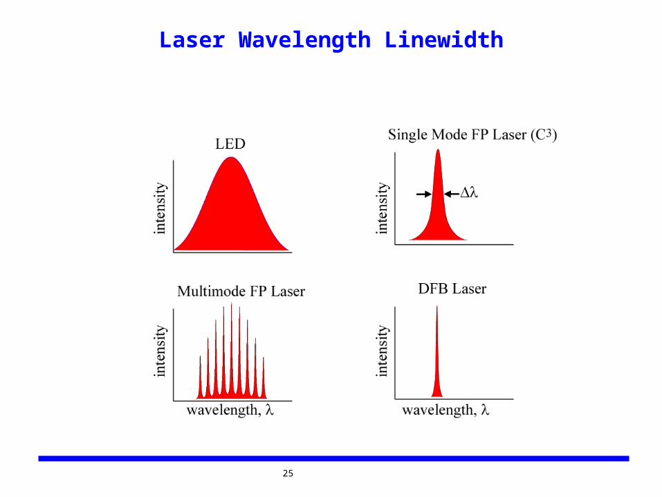
Laser Wavelength Linewidth
26
Summary of Source Characteristics
• Laser type
– FP laser: Less expensive, larger linewidth
– DFB: More expensive, smaller linewidth
• Optical characteristics
– Optical wavelength
– Optical linewidth
– Optical power
• Electrical characteristics
– Electrical power consumption
– Required voltage
– Required current
27
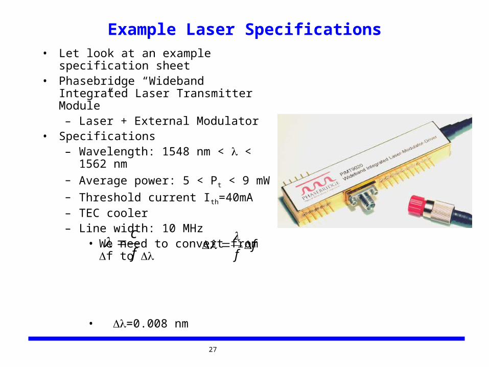
Example Laser Specifications• Let look at an example specification sheet• Phasebridge “Wideband Integrated Laser
Transmitter Module”– Laser + External Modulator
• Specifications– Wavelength: 1548 nm < < 1562 nm– Average power: 5 < Pt < 9 mW– Threshold current Ith=40mA– TEC cooler– Line width: 10 MHz
• We need to convert from f to
• =0.008 nm
f
c f
f
28
Semiconductor Optical Detectors
29
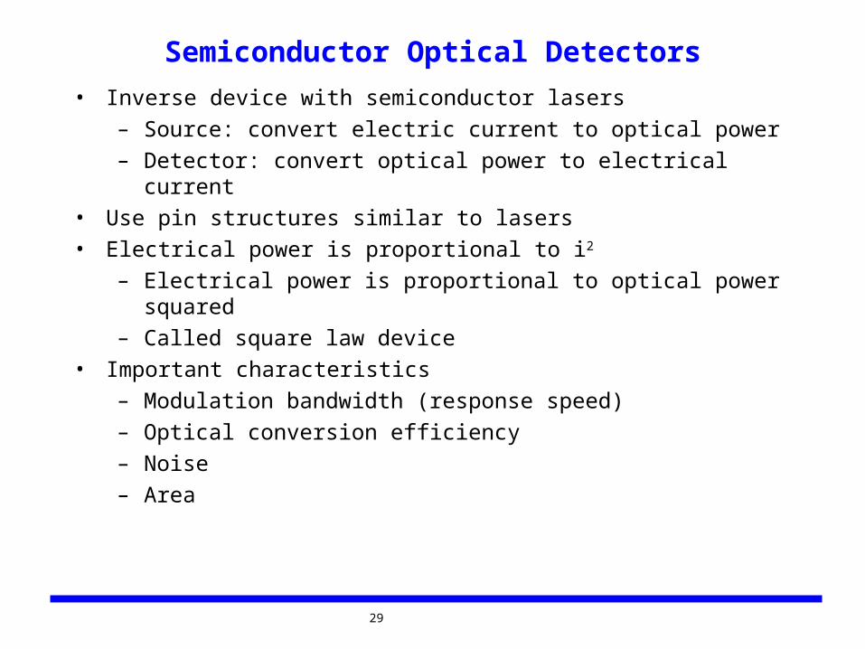
Semiconductor Optical Detectors
• Inverse device with semiconductor lasers
– Source: convert electric current to optical power
– Detector: convert optical power to electrical current
• Use pin structures similar to lasers
• Electrical power is proportional to i2
– Electrical power is proportional to optical power squared
– Called square law device
• Important characteristics
– Modulation bandwidth (response speed)
– Optical conversion efficiency
– Noise
– Area
30
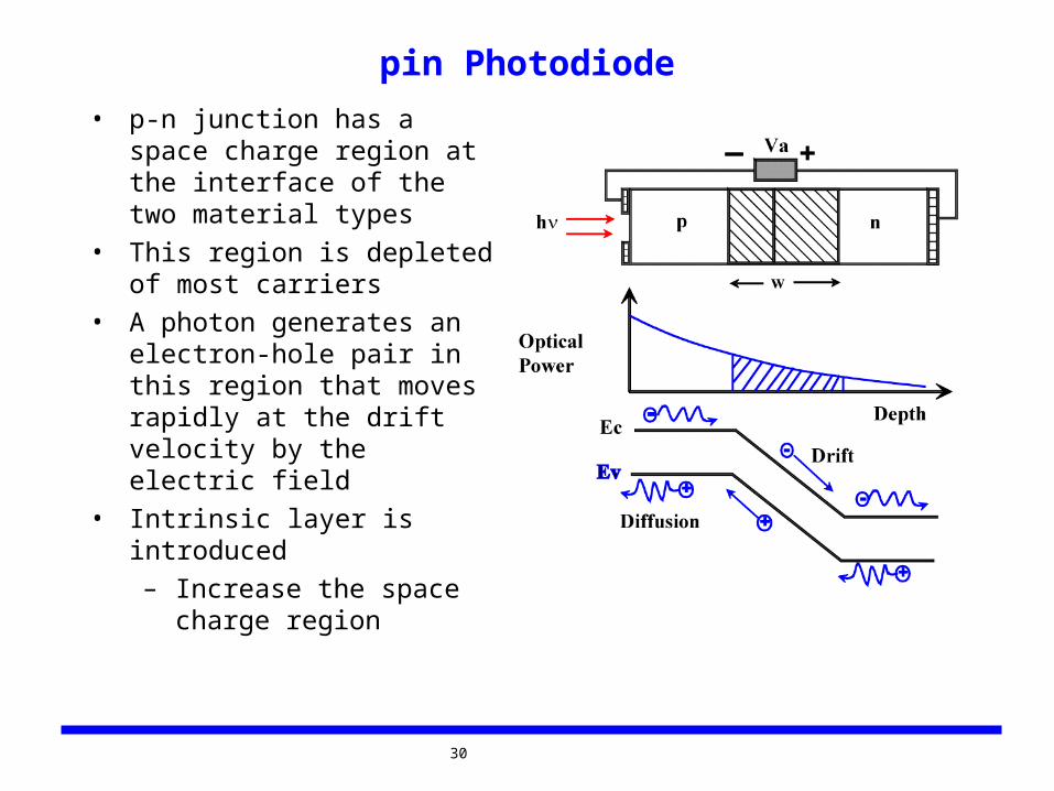
pin Photodiode
• p-n junction has a space charge region at the interface of the two material types
• This region is depleted of most carriers
• A photon generates an electron-hole pair in this region that moves rapidly at the drift velocity by the electric field
• Intrinsic layer is introduced
– Increase the space charge region
31
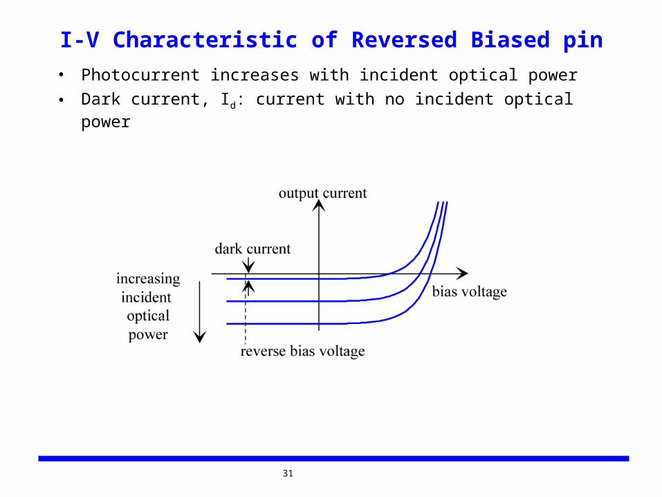
I-V Characteristic of Reversed Biased pin
• Photocurrent increases with incident optical power
• Dark current, Id: current with no incident optical power
32
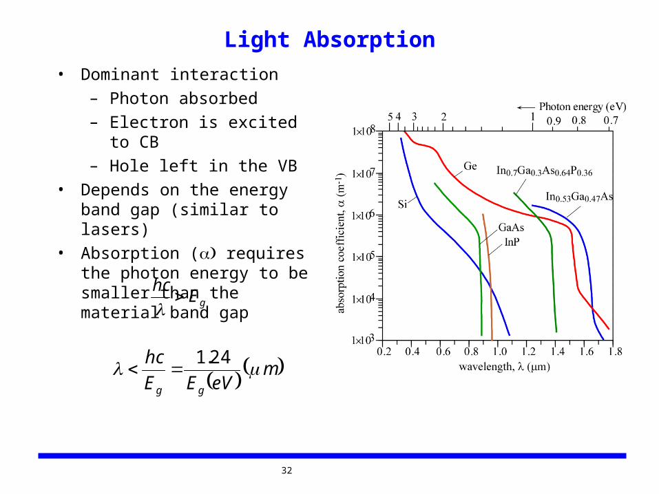
Light Absorption
• Dominant interaction
– Photon absorbed
– Electron is excited to CB
– Hole left in the VB
• Depends on the energy band gap (similar to lasers)
• Absorption ( requires the photon energy to be smaller than the material band gap
gEhc
meVEE
hc
gg
24.1
33
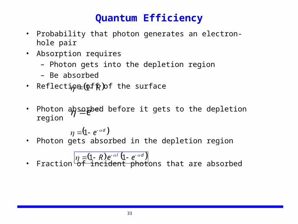
Quantum Efficiency
• Probability that photon generates an electron-hole pair
• Absorption requires
– Photon gets into the depletion region
– Be absorbed
• Reflection off of the surface
• Photon absorbed before it gets to the depletion region
• Photon gets absorbed in the depletion region
• Fraction of incident photons that are absorbed
le
R 1
de 1
dl eeR 11
34
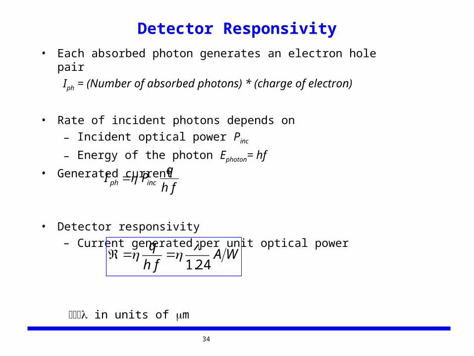
Detector Responsivity
• Each absorbed photon generates an electron hole pair
Iph = (Number of absorbed photons) * (charge of electron)
• Rate of incident photons depends on
– Incident optical power Pinc
– Energy of the photon Ephoton= hf
• Generated current
• Detector responsivity
– Current generated per unit optical power
in units of m
fh
qPI incph
WAfh
q
24.1
35
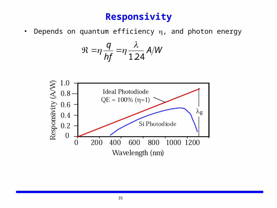
Responsivity
• Depends on quantum efficiency , and photon energy
WAhf
q
24.1
36
Avalanche Photodiode (APD)
37
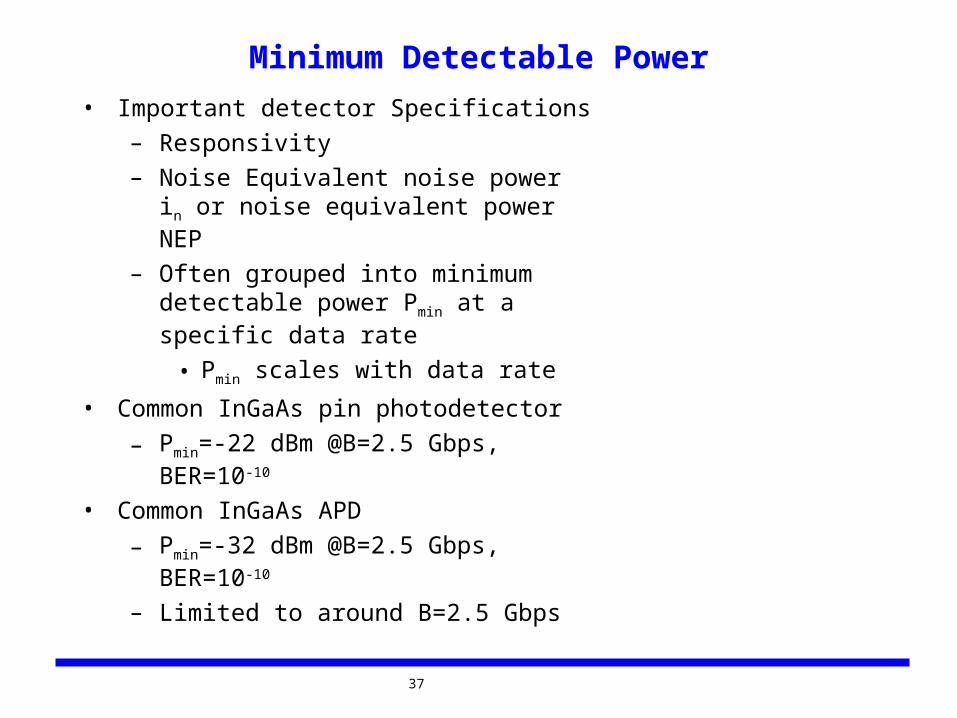
Minimum Detectable Power
• Important detector Specifications
– Responsivity
– Noise Equivalent noise power in or noise equivalent power NEP
– Often grouped into minimum detectable power Pmin at a specific data rate
• Pmin scales with data rate
• Common InGaAs pin photodetector
– Pmin=-22 dBm @B=2.5 Gbps, BER=10-10
• Common InGaAs APD
– Pmin=-32 dBm @B=2.5 Gbps, BER=10-10
– Limited to around B=2.5 Gbps


![Specification - Digi-Key Sheets/Seoul Semiconductor/LY521... · Outline Dimensions 8. Packing 9. Soldering ... Optical Efficiency ŋelc - 50 - lm/W ... Dominant Wavelength[5] λd](https://img.pdfslide.us/doc/110x75/5b50389b7f8b9a396e8e045e/specification-digi-key-sheetsseoul-semiconductorly521-outline-dimensions.jpg)