Embed Size (px)
Citation preview
Basics of RF Devices I
OUTLINE• Introduction • Mainstream Electronics vs RF Electronics• Transistor Concepts I• RF Transistor Figures of Merit• Material Issues – Special Needs for RF• History and Evolution of RF Transistors
Frank Schwierz Technische Universität Ilmenau, Germany
TARGET Summer School, 13 September 2004Europa Beach, Crete 1
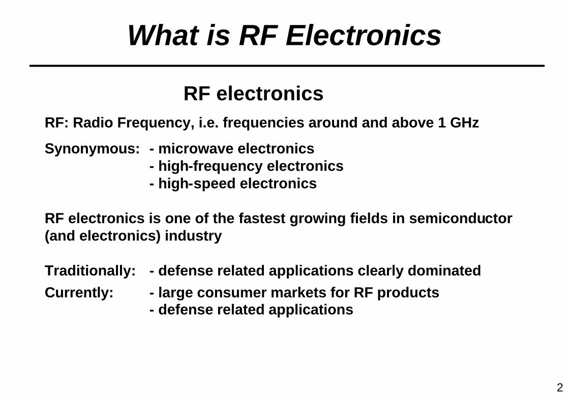
What is RF Electronics
RF electronicsRF: Radio Frequency, i.e. frequencies around and above 1 GHz
Synonymous: - microwave electronics- high-frequency electronics- high-speed electronics
RF electronics is one of the fastest growing fields in semiconductor(and electronics) industry
Traditionally: - defense related applications clearly dominatedCurrently: - large consumer markets for RF products
- defense related applications
2
Basics of RF Devices I
OUTLINE• Introduction • Mainstream Electronics vs. RF Electronics• Transistor Concepts I• RF Transistor Figures of Merit• Material Issues – Special Needs for RF• History and Evolution of RF Transistors
Frank Schwierz Technische Universität Ilmenau, Germany
TARGET Summer School, 13 September 2004Europa Beach, Crete 3
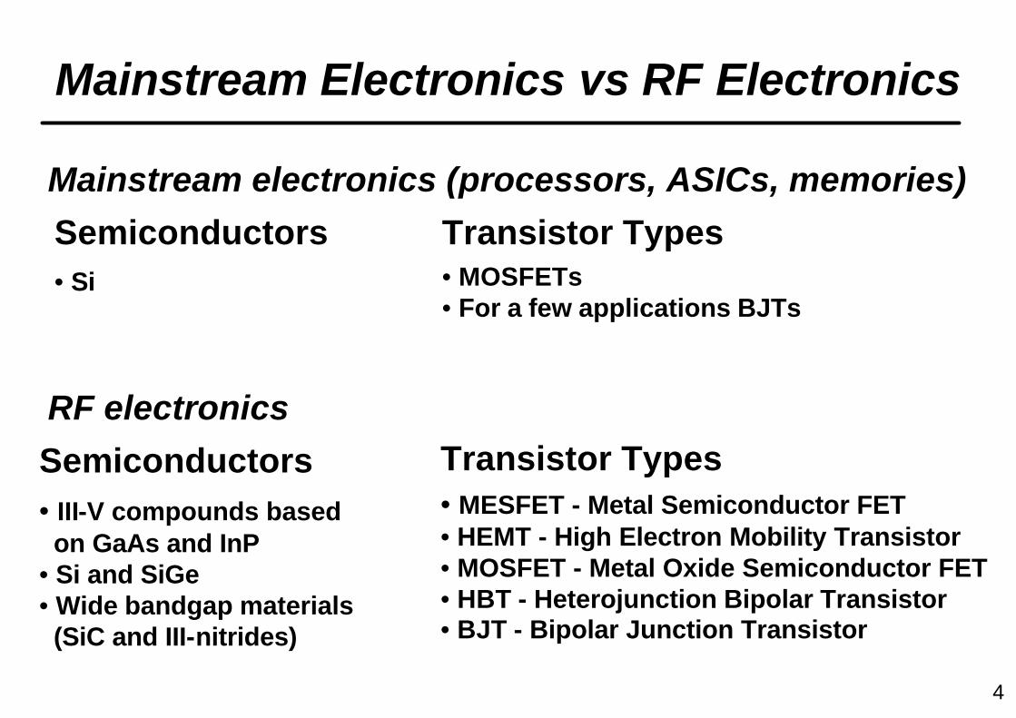
Mainstream Electronics vs RF Electronics
Semiconductors• III-V compounds basedon GaAs and InP
• Si and SiGe• Wide bandgap materials(SiC and III-nitrides)
Transistor Types• MESFET - Metal Semiconductor FET• HEMT - High Electron Mobility Transistor• MOSFET - Metal Oxide Semiconductor FET • HBT - Heterojunction Bipolar Transistor• BJT - Bipolar Junction Transistor
Mainstream electronics (processors, ASICs, memories)
Semiconductors• Si
Transistor Types• MOSFETs• For a few applications BJTs
RF electronics
4
Mainstream Electronics vs RF Electronics
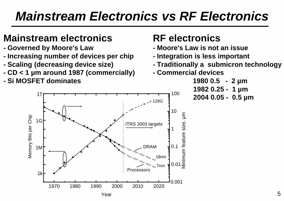
Mainstream electronics - Governed by Moore's Law- Increasing number of devices per chip- Scaling (decreasing device size)- CD < 1 µm around 1987 (commercially)- Si MOSFET dominates
1970 1980 1990 2000 2010 2020
1T
1G
1M
1k
Min
imum
feat
ure
size
, µm
Mem
ory
Bits
per
Chi
p
Year
0.01
0.1
1
10
100128G
0.001
DRAM
Processors7nm
18nm
ITRS 2003 targets
RF electronics - Moore's Law is not an issue- Integration is less important- Traditionally a submicron technology- Commercial devices
1980 0.5 - 2 µm1982 0.25 - 1 µm2004 0.05 - 0.5 µm
5
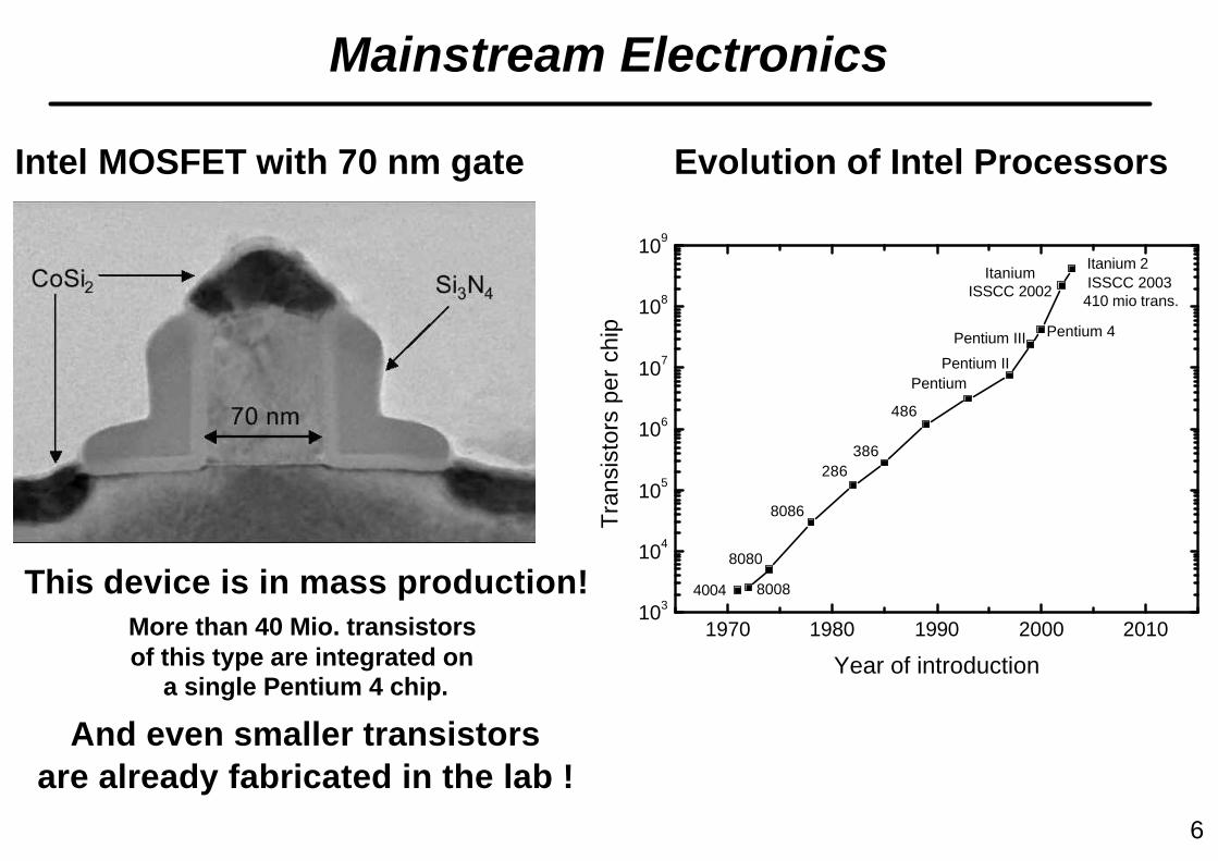
Intel MOSFET with 70 nm gate Evolution of Intel Processors
This device is in mass production!More than 40 Mio. transistors of this type are integrated on
a single Pentium 4 chip.
And even smaller transistors are already fabricated in the lab !
Mainstream Electronics
1970 1980 1990 2000 2010103
104
105
106
107
108
109
Itanium 2 ISSCC 2003410 mio trans.
ItaniumISSCC 2002
Pentium 4Pentium III
Pentium IIPentium
486
286386
8086
8080
80084004T
rans
isto
rs p
er c
hip
Year of introduction
6
Mainstream Electronics
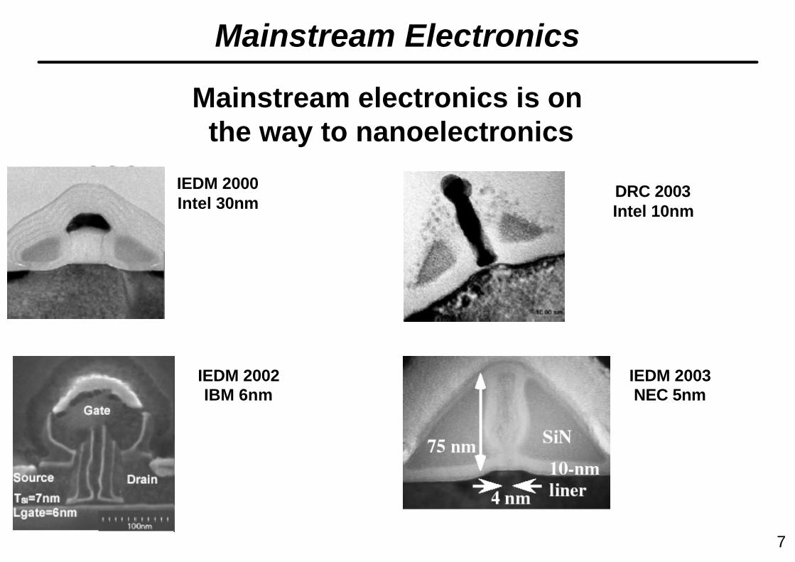
Mainstream electronics is on the way to nanoelectronics
IEDM 2000Intel 30nm
DRC 2003Intel 10nm
IEDM 2002IBM 6nm
IEDM 2003NEC 5nm
7
Mainstream Electronics
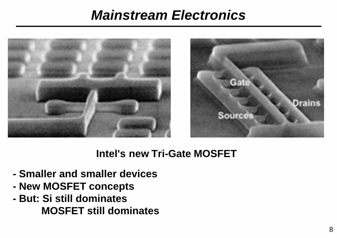
Intel's new Tri-Gate MOSFET
- Smaller and smaller devices- New MOSFET concepts- But: Si still dominates
MOSFET still dominates
8
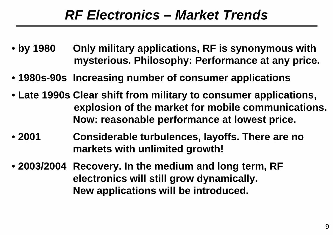
RF Electronics – Market Trends
• by 1980 Only military applications, RF is synonymous withmysterious. Philosophy: Performance at any price.
• 1980s-90s Increasing number of consumer applications
• Late 1990s Clear shift from military to consumer applications, explosion of the market for mobile communications.Now: reasonable performance at lowest price.
• 2001 Considerable turbulences, layoffs. There are no markets with unlimited growth!
• 2003/2004 Recovery. In the medium and long term, RF electronics will still grow dynamically. New applications will be introduced.
9
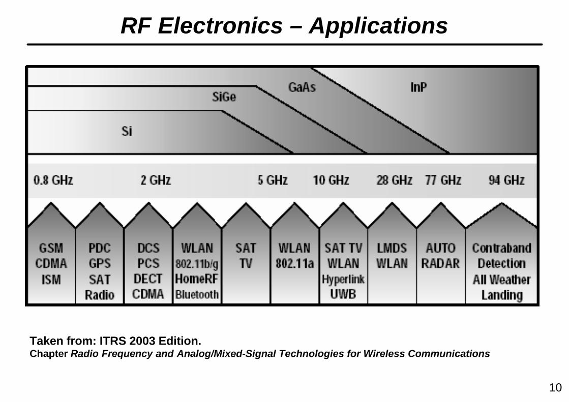
RF Electronics – Applications
Taken from: ITRS 2003 Edition. Chapter Radio Frequency and Analog/Mixed-Signal Technologies for Wireless Communications
10
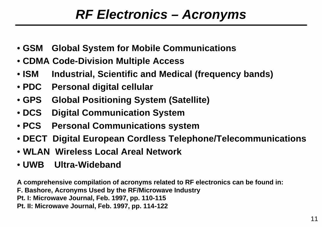
RF Electronics – Acronyms
• GSM Global System for Mobile Communications• CDMA Code-Division Multiple Access• ISM Industrial, Scientific and Medical (frequency bands)• PDC Personal digital cellular• GPS Global Positioning System (Satellite)• DCS Digital Communication System• PCS Personal Communications system• DECT Digital European Cordless Telephone/Telecommunications• WLAN Wireless Local Areal Network• UWB Ultra-Wideband
A comprehensive compilation of acronyms related to RF electronics can be found in: F. Bashore, Acronyms Used by the RF/Microwave Industry Pt. I: Microwave Journal, Feb. 1997, pp. 110-115Pt. II: Microwave Journal, Feb. 1997, pp. 114-122
11
Basics of RF Devices I
OUTLINE• Introduction • Mainstream Electronics vs. RF Electronics• Transistor Concepts I• RF Transistor Figures of Merit• Material Issues – Special Needs for RF• History and Evolution of RF Transistors
Frank Schwierz Technische Universität Ilmenau, Germany
TARGET Summer School, 13 September 2004Europa Beach, Crete 12
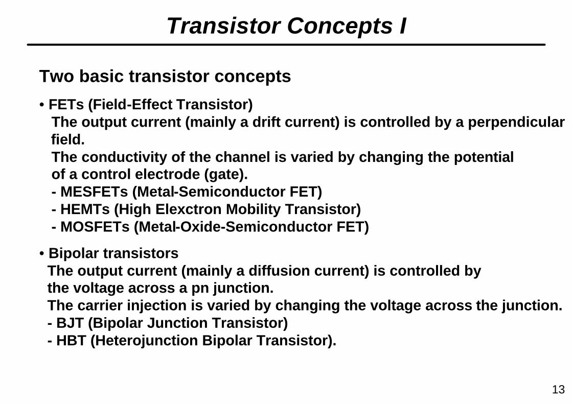
Transistor Concepts I
Two basic transistor concepts
• FETs (Field-Effect Transistor)The output current (mainly a drift current) is controlled by a perpendicularfield.The conductivity of the channel is varied by changing the potential of a control electrode (gate).- MESFETs (Metal-Semiconductor FET)- HEMTs (High Elexctron Mobility Transistor)- MOSFETs (Metal-Oxide-Semiconductor FET)
• Bipolar transistorsThe output current (mainly a diffusion current) is controlled by the voltage across a pn junction.The carrier injection is varied by changing the voltage across the junction.- BJT (Bipolar Junction Transistor)- HBT (Heterojunction Bipolar Transistor).
13
Transistor Concepts I - FETs
Channelbulk-like
Channel 2DEG
S G D S G D
S.I. GaAsS.I. GaAs
EC
EF
EV
EC
EF
EV
n+ n+ n+ n+n AlGaAs
i GaAs
Channel 2DEG
S G D
p-type Si
EC
EF
EV
n+ n+
Inversion layer
MESFET HEMT MOSFET
Source Drain
Gate
VG
Lch n+ n+
Channel
A FET in general
FETs
14
RF FETs use n-channels.A more positive gate voltage increases the number of carriers (electrons) in the channel
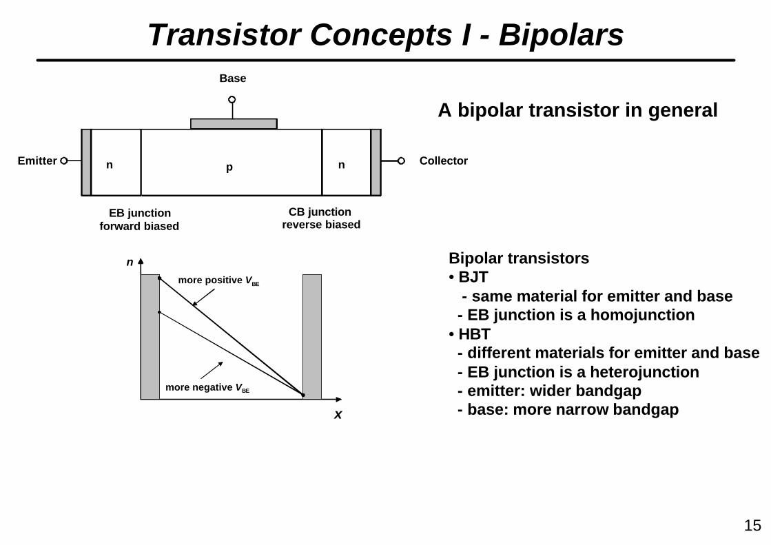
Transistor Concepts I - Bipolars
A bipolar transistor in general
Emitter Collector
Base
n np
EB junctionforward biased
CB junctionreverse biased
n
x
more positive VBE
more negative VBE
Bipolar transistors• BJT
- same material for emitter and base- EB junction is a homojunction
• HBT- different materials for emitter and base- EB junction is a heterojunction- emitter: wider bandgap- base: more narrow bandgap
15
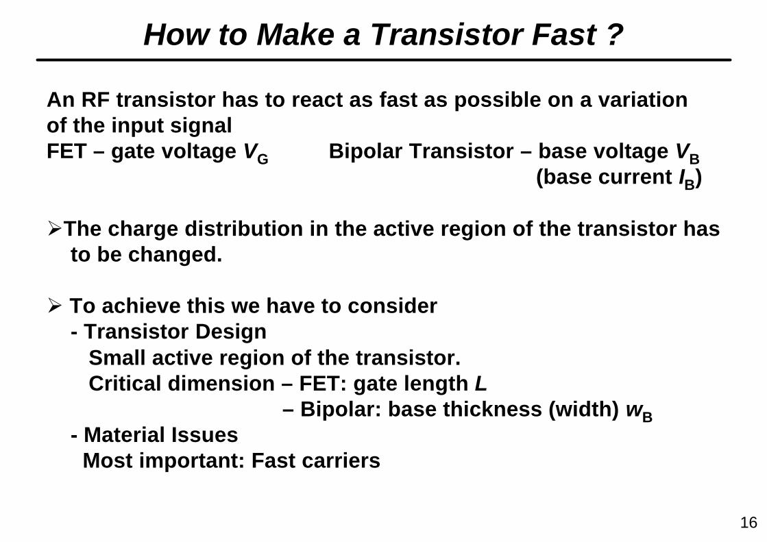
An RF transistor has to react as fast as possible on a variationof the input signalFET – gate voltage VG Bipolar Transistor – base voltage VB
(base current IB)
ØThe charge distribution in the active region of the transistor hasto be changed.
Ø To achieve this we have to consider- Transistor Design
Small active region of the transistor. Critical dimension – FET: gate length L
– Bipolar: base thickness (width) wB- Material Issues
Most important: Fast carriers
How to Make a Transistor Fast ?
16
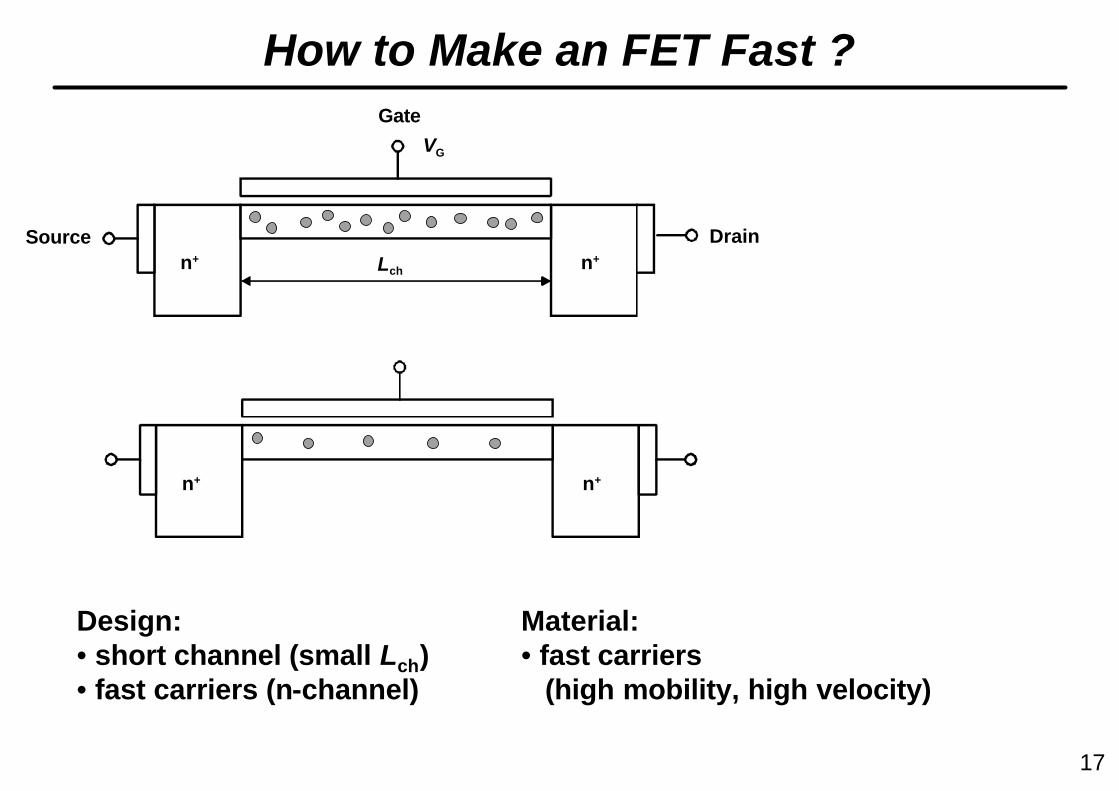
How to Make an FET Fast ?
Source Drain
GateVG
n+ n+
Lch n+ n+
Design: • short channel (small Lch)• fast carriers (n-channel)
Material: • fast carriers
(high mobility, high velocity)
17
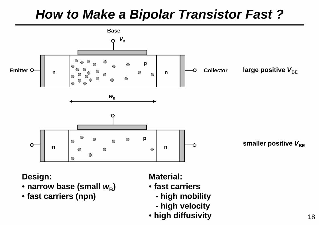
How to Make a Bipolar Transistor Fast ?
Emitter Collector
Base
VB
n n
wB
p
n n
p
large positive VBE
smaller positive VBE
Design: • narrow base (small wB)• fast carriers (npn)
Material: • fast carriers
- high mobility- high velocity
• high diffusivity 18
Basics of RF Devices I
OUTLINE• Introduction • Mainstream Electronics vs. RF Electronics• Transistor Concepts I• RF Transistor Figures of Merit• Material Issues – Special Needs for RF• History and Evolution of RF Transistors
Frank Schwierz Technische Universität Ilmenau, Germany
TARGET Summer School, 13 September 2004Europa Beach, Crete 19
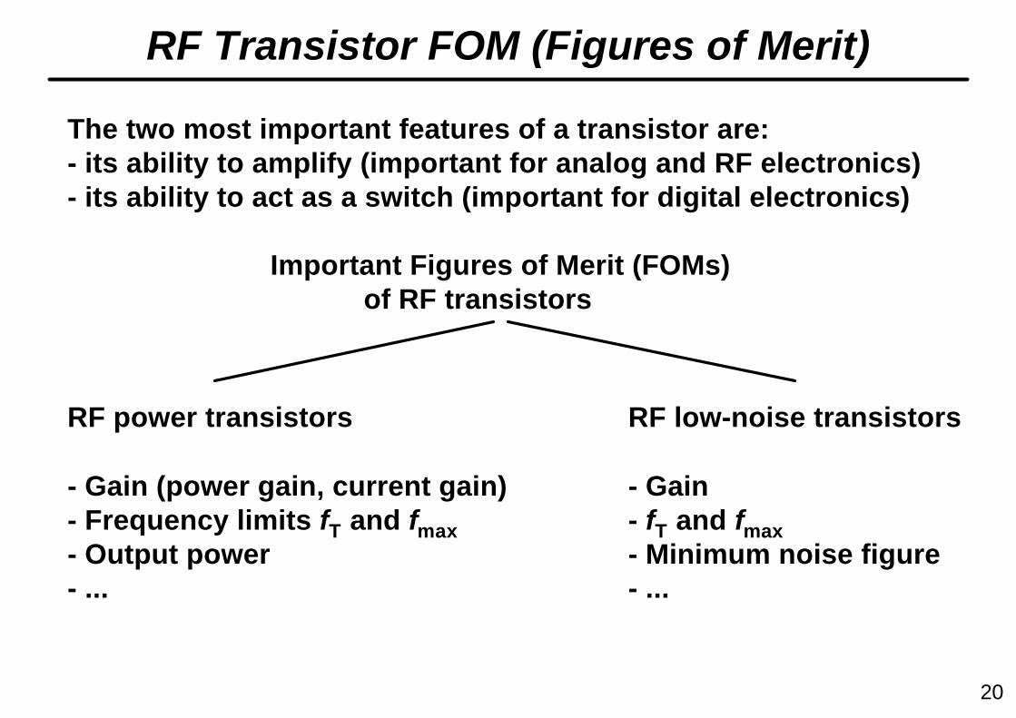
RF Transistor FOM (Figures of Merit)
The two most important features of a transistor are:- its ability to amplify (important for analog and RF electronics)- its ability to act as a switch (important for digital electronics)
Important Figures of Merit (FOMs)of RF transistors
RF power transistors RF low-noise transistors
- Gain (power gain, current gain) - Gain- Frequency limits fT and fmax - fT and fmax- Output power - Minimum noise figure- ... - ...
20
FOMs – Power Gains
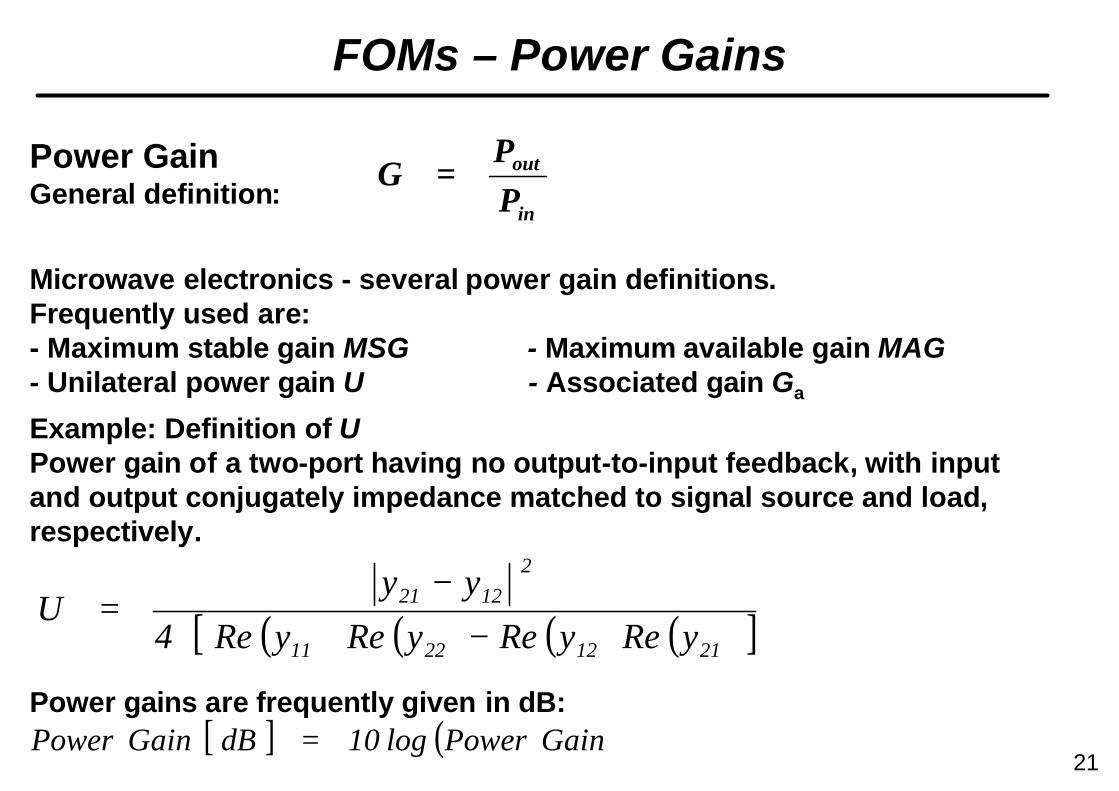
Power GainGeneral definition:
Microwave electronics - several power gain definitions.Frequently used are:- Maximum stable gain MSG - Maximum available gain MAG- Unilateral power gain U - Associated gain Ga
Example: Definition of UPower gain of a two-port having no output-to-input feedback, with input and output conjugately impedance matched to signal source and load, respectively.
Power gains are frequently given in dB:
in
out
PP
G =
( ) ( ) ( ) ( )[ ]21122211
21221
yReyReyReyRe4
yyU
−−
=
[ ] ( )GainPowerlog10dBGainPower =21
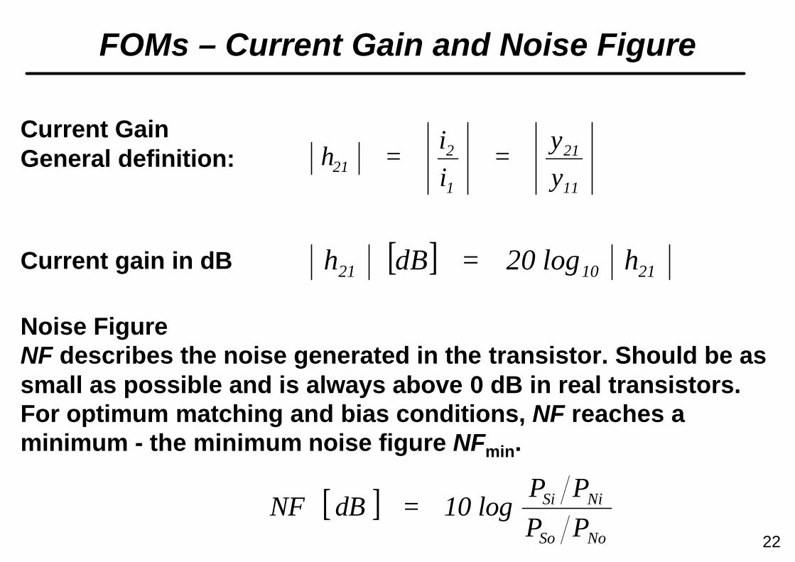
Current GainGeneral definition:
Current gain in dB
Noise FigureNF describes the noise generated in the transistor. Should be as small as possible and is always above 0 dB in real transistors. For optimum matching and bias conditions, NF reaches a minimum - the minimum noise figure NFmin.
FOMs – Current Gain and Noise Figure
11
21
1
221 y
yii
h ==
[ ] 211021 hlog20dBh =
[ ]NoSo
NiSi
PPPP
log10dBNF =22
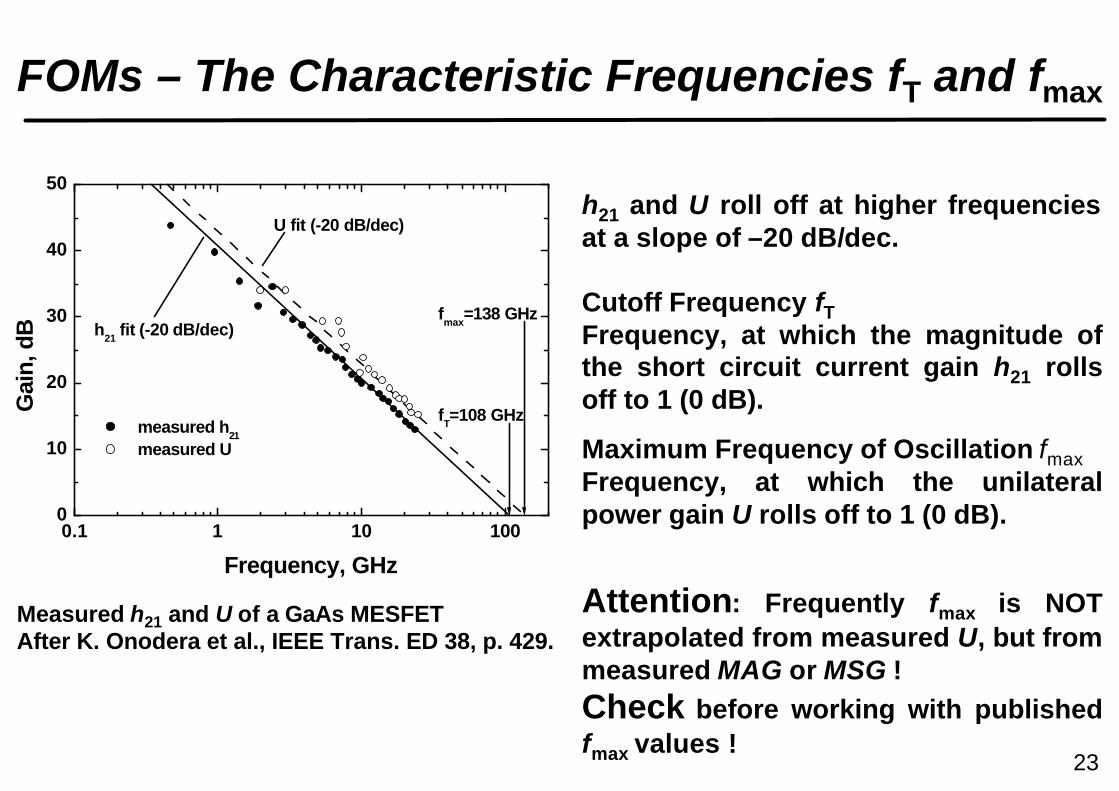
FOMs – The Characteristic Frequencies fT and fmax
0.1 1 10 1000
10
20
30
40
50
fmax
=138 GHz
fT=108 GHz
U fit (-20 dB/dec)
h21
fit (-20 dB/dec)
Gai
n, d
B
measured h21
measured U
Frequency, GHz
h21 and U roll off at higher frequencies at a slope of –20 dB/dec.
Cutoff Frequency fTFrequency, at which the magnitude of the short circuit current gain h21 rolls off to 1 (0 dB).
Maximum Frequency of Oscillation fmaxFrequency, at which the unilateral power gain U rolls off to 1 (0 dB).
Attention: Frequently fmax is NOT extrapolated from measured U, but from measured MAG or MSG ! Check before working with published fmax values !
Measured h21 and U of a GaAs MESFETAfter K. Onodera et al., IEEE Trans. ED 38, p. 429.
23
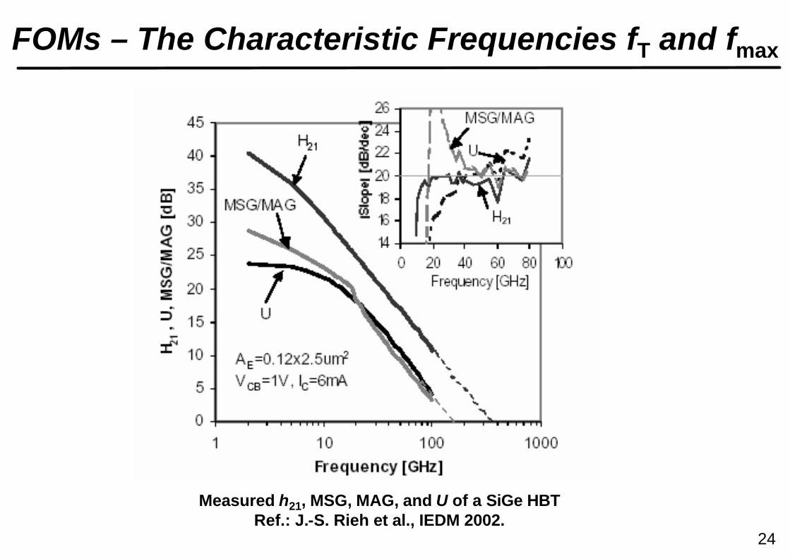
FOMs – The Characteristic Frequencies fT and fmax
Measured h21, MSG, MAG, and U of a SiGe HBTRef.: J.-S. Rieh et al., IEDM 2002.
24
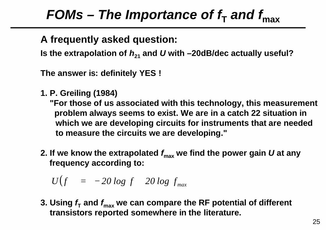
FOMs – The Importance of fT and fmax
A frequently asked question:Is the extrapolation of h21 and U with –20dB/dec actually useful?
The answer is: definitely YES !
1. P. Greiling (1984)"For those of us associated with this technology, this measurement problem always seems to exist. We are in a catch 22 situation in which we are developing circuits for instruments that are needed to measure the circuits we are developing."
2. If we know the extrapolated fmax we find the power gain U at anyfrequency according to:
3. Using fT and fmax we can compare the RF potential of differenttransistors reported somewhere in the literature.
( ) maxflog20flog20fU +−=
25
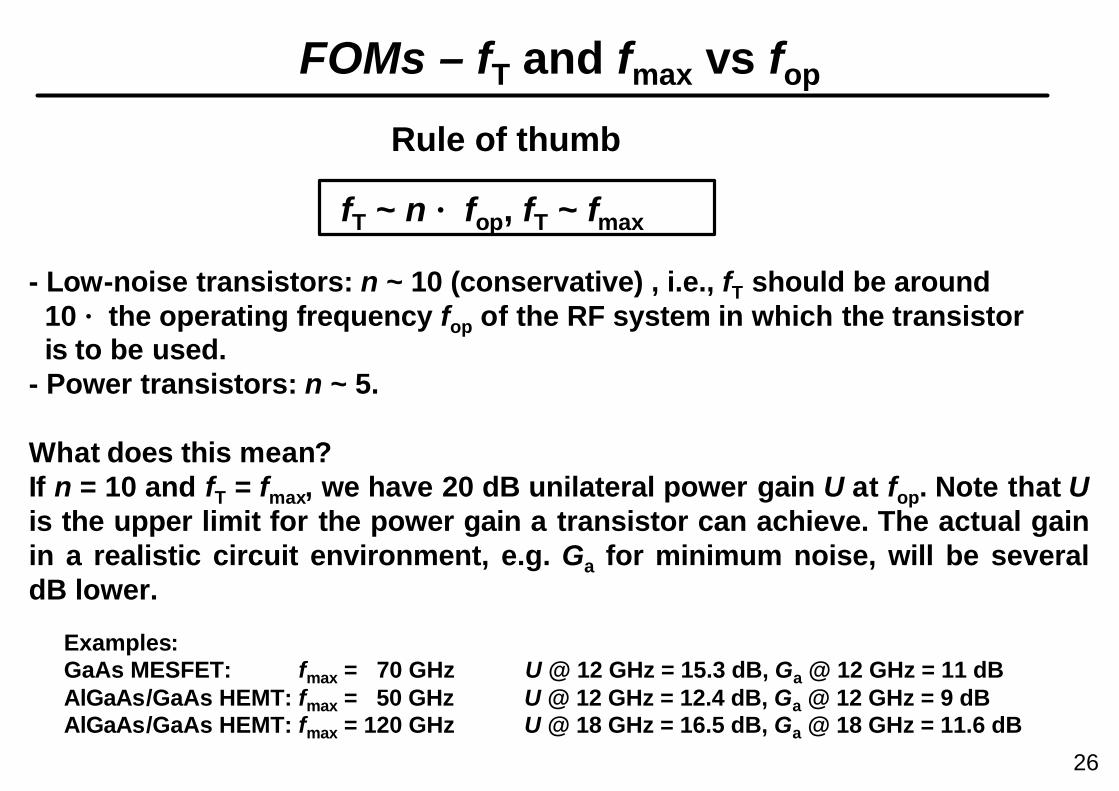
FOMs – fT and fmax vs fop
Rule of thumb
fT ~ n × fop, fT ~ fmax
- Low-noise transistors: n ~ 10 (conservative) , i.e., fT should be around 10 × the operating frequency fop of the RF system in which the transistoris to be used.
- Power transistors: n ~ 5.
What does this mean? If n = 10 and fT = fmax, we have 20 dB unilateral power gain U at fop. Note that Uis the upper limit for the power gain a transistor can achieve. The actual gain in a realistic circuit environment, e.g. Ga for minimum noise, will be several dB lower.
Examples: GaAs MESFET: fmax = 70 GHz U @ 12 GHz = 15.3 dB, Ga @ 12 GHz = 11 dBAlGaAs/GaAs HEMT: fmax = 50 GHz U @ 12 GHz = 12.4 dB, Ga @ 12 GHz = 9 dBAlGaAs/GaAs HEMT: fmax = 120 GHz U @ 18 GHz = 16.5 dB, Ga @ 18 GHz = 11.6 dB
26
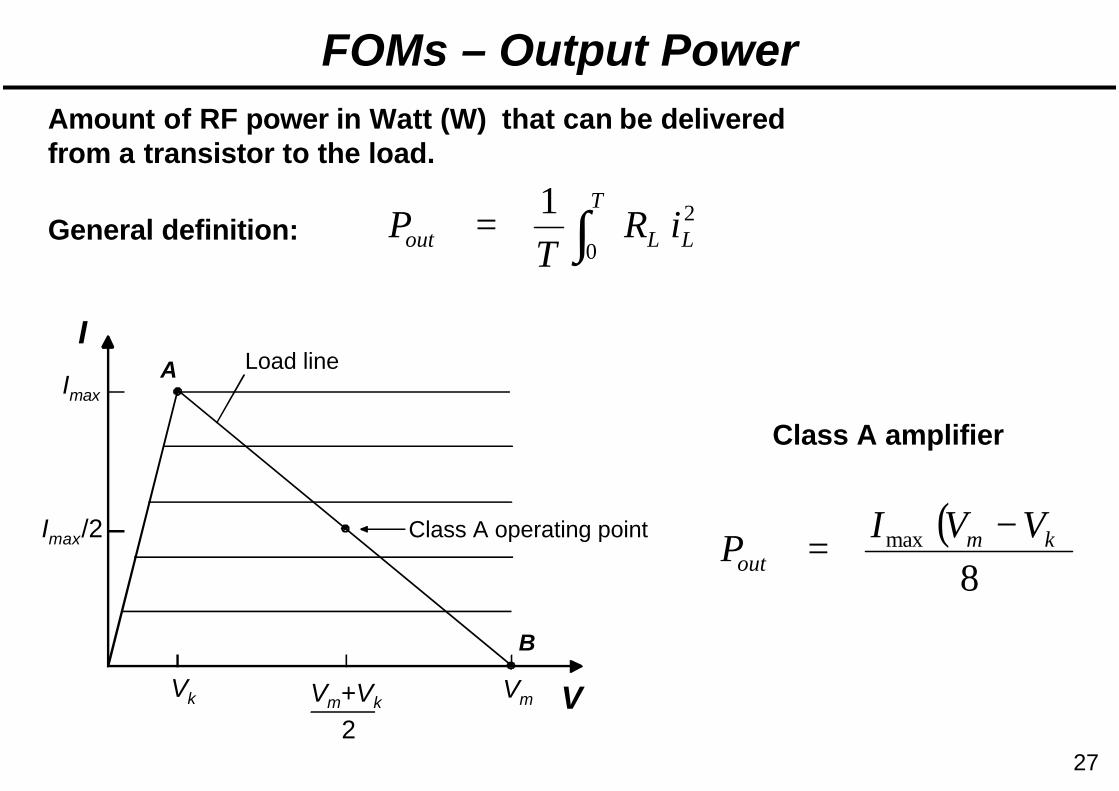
FOMs – Output Power Amount of RF power in Watt (W) that can be deliveredfrom a transistor to the load.
General definition: ∫=T
LLout iRT
P0
21
27
I
Imax
Imax /2
Load line
Class A operating point
Vk VVmVm+Vk
2
A
B
( )8
max kmout
VVIP
−=
Class A amplifier
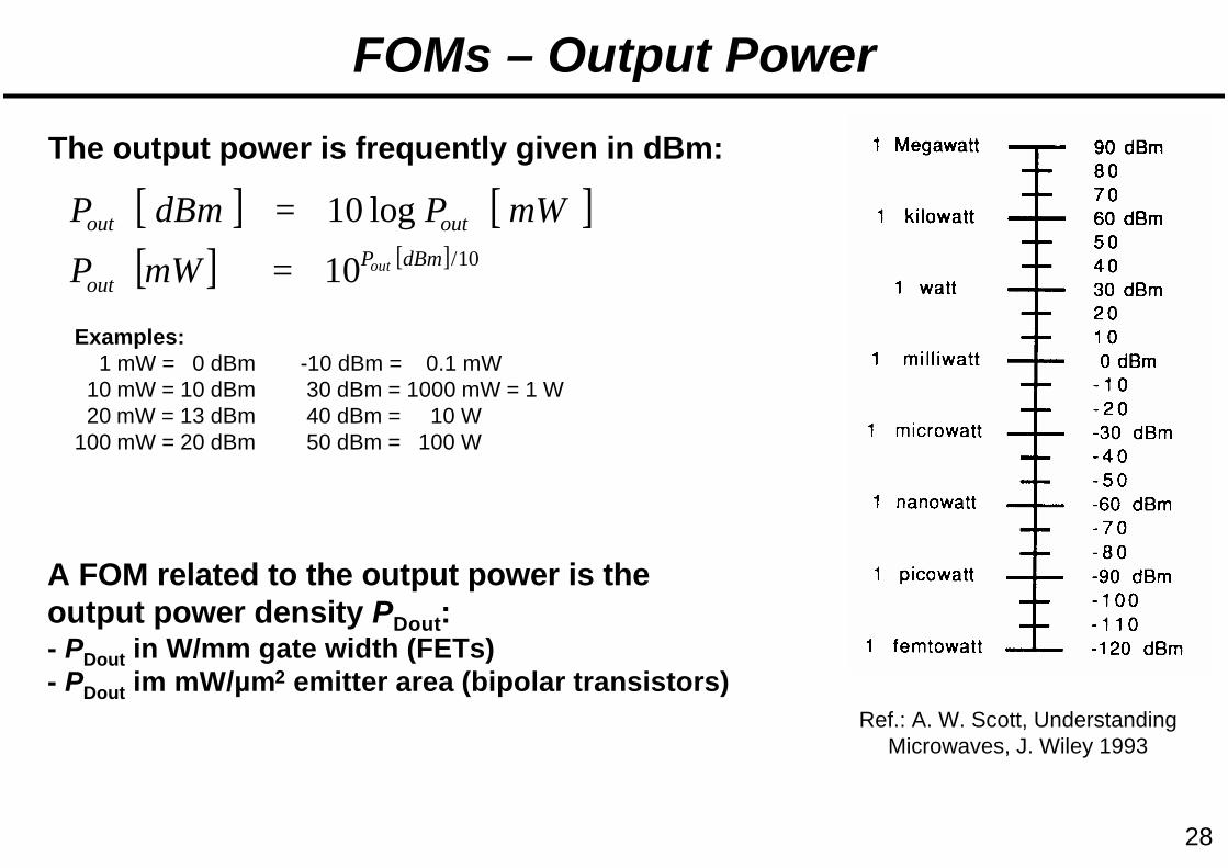
FOMs – Output Power
[ ] [ ][ ] [ ] 10/10
log10dBmP
out
outout
outmWP
mWPdBmP
=
=
Examples:1 mW = 0 dBm -10 dBm = 0.1 mW
10 mW = 10 dBm 30 dBm = 1000 mW = 1 W20 mW = 13 dBm 40 dBm = 10 W
100 mW = 20 dBm 50 dBm = 100 W
The output power is frequently given in dBm:
Ref.: A. W. Scott, Understanding Microwaves, J. Wiley 1993
A FOM related to the output power is theoutput power density PDout:- PDout in W/mm gate width (FETs)- PDout im mW/µm2 emitter area (bipolar transistors)
28
Basics of RF Devices I
OUTLINE• Introduction • Mainstream Electronics vs. RF Electronics• Transistor Concepts I• RF Transistor Figures of Merit• Material Issues – Special Needs for RF• History and Evolution of RF Transistors
Frank Schwierz Technische Universität Ilmenau, Germany
TARGET Summer School, 13 September 2004Europa Beach, Crete 29
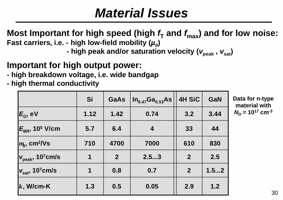
Material IssuesMost Important for high speed (high fT and fmax) and for low noise:Fast carriers, i.e. - high low-field mobility (µ0)
- high peak and/or saturation velocity (vpeak , vsat)
Important for high output power:- high breakdown voltage, i.e. wide bandgap- high thermal conductivity
1.22.90.050.51.3κ, W/cm-K
1.5...220.70.81vsat, 107cm/s
2.522.5...321vpeak, 107cm/s
83061070004700710µ0, cm2/Vs
443346.45.7EBR, 105 V/cm
3.443.20.741.421.12EG, eV
GaN4H SiCIn0.47Ga0.53AsGaAsSi Data for n-typematerial withND = 1017 cm-3
30
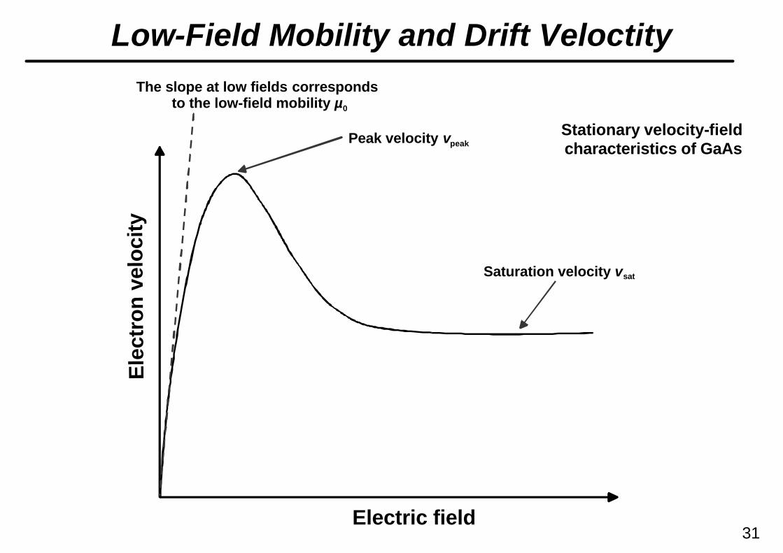
Low-Field Mobility and Drift Veloctity
31
Ele
ctro
n v
elo
city
Electric field
The slope at low fields corresponds to the low-field mobility µ0
Peak velocity vpeak
Saturation velocity vsat
Stationary velocity-field characteristics of GaAs
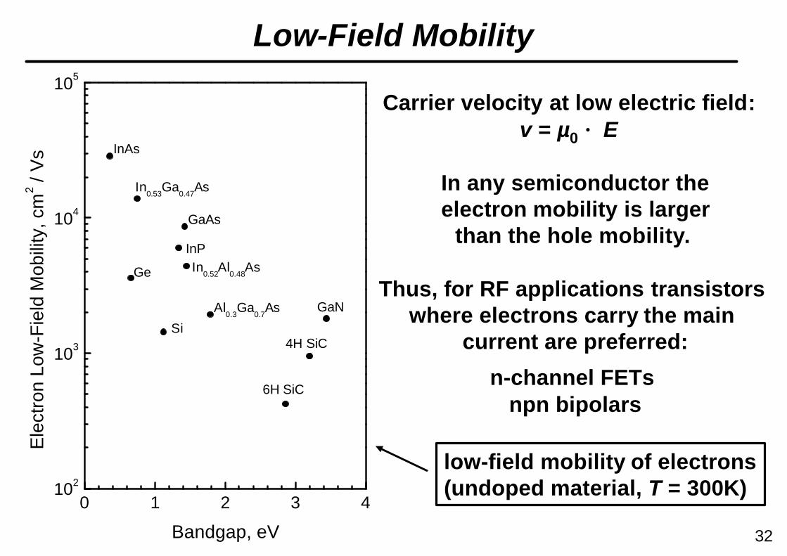
Low-Field Mobility
0 1 2 3 4102
103
104
105
GaN
4H SiC
6H SiC
Al0.3
Ga0.7
As
In0.52
Al0.48
As
GaAs
InP
Si
Ge
In0.53
Ga0.47
As
InAs
Ele
ctro
n Lo
w-F
ield
Mob
ility
, cm
2 / V
s
Bandgap, eV
In any semiconductor theelectron mobility is larger
than the hole mobility.
Thus, for RF applications transistors where electrons carry the main
current are preferred:
n-channel FETs npn bipolars
Carrier velocity at low electric field:v = µ0 × E
low-field mobility of electrons(undoped material, T = 300K)
32
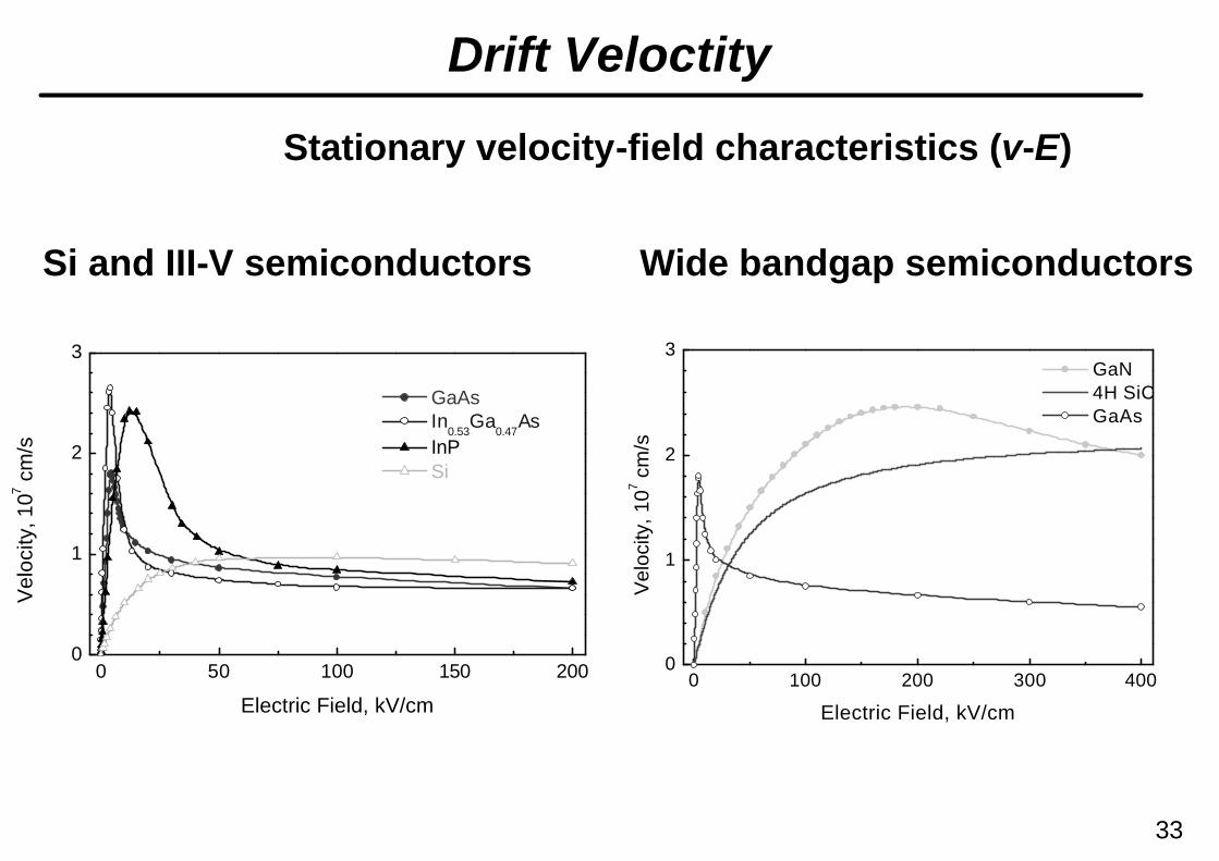
Si and III-V semiconductors Wide bandgap semiconductors
Drift Veloctity
Stationary velocity-field characteristics (v-E)
0 50 100 150 2000
1
2
3
GaAs In
0.53Ga
0.47As
InP Si
Vel
ocity
, 107 c
m/s
Electric Field, kV/cm0 100 200 300 400
0
1
2
3
GaN 4H SiC GaAs
Vel
ocity
, 107 c
m/s
Electric Field, kV/cm
33
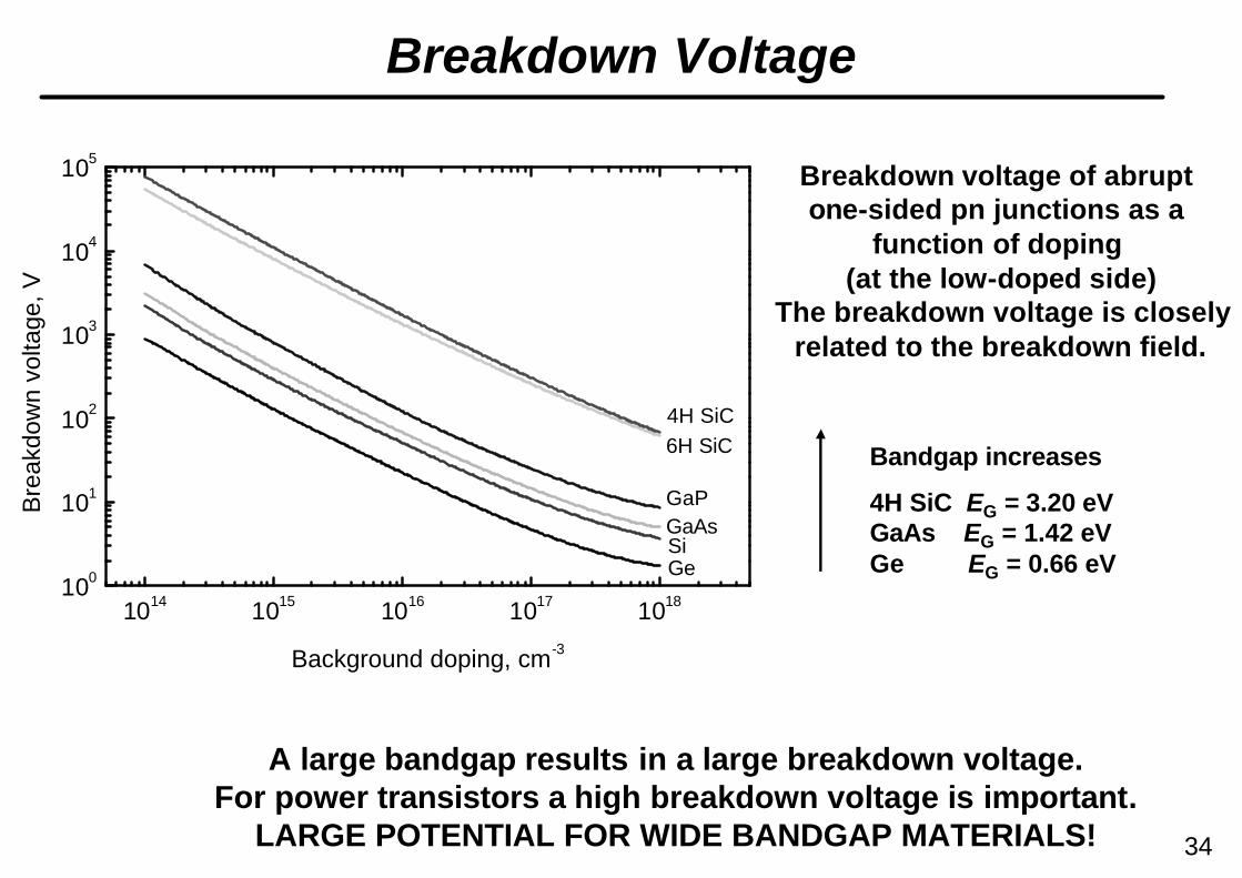
Breakdown Voltage
A large bandgap results in a large breakdown voltage.For power transistors a high breakdown voltage is important.
LARGE POTENTIAL FOR WIDE BANDGAP MATERIALS!
Breakdown voltage of abrupt one-sided pn junctions as a
function of doping (at the low-doped side)
The breakdown voltage is closelyrelated to the breakdown field.
Bandgap increases
4H SiC EG = 3.20 eVGaAs EG = 1.42 eVGe EG = 0.66 eV
34
1014 1015 1016 1017 1018100
101
102
103
104
105
4H SiC6H SiC
GaPGaAsSiGe
Bre
akdo
wn
volta
ge, V
Background doping, cm-3
Heterostructures
Heterostructures Ø are semiconductor structures consisting of at least
two different semiconductors
Ø are uncommon in mainstream electronics
Ø are frequently used in RF transistors- FETs: HEMTs- Bipolars: HBTs
Ø The RF transistors showing- the highest fT and fmax- the highest output power densities- the lowest noiseare heterostructure transistors.
Therefore it is useful to discuss some aspects ofheterostructures in the following.
35
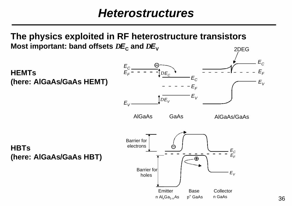
Heterostructures
EF
EV
EC
EF
EV
EC
AlGaAs GaAs
EF
EV
EC
2DEG
AlGaAs/GaAs
∆ EC
∆ EV
EF
EV
EC
Barrier for electrons
Barrier for holes
Emitter Base Collectorn AlxGa1-x As n GaAsp+ GaAs
The physics exploited in RF heterostructure transistorsMost important: band offsets ∆EC and ∆EV
HEMTs(here: AlGaAs/GaAs HEMT)
HBTs(here: AlGaAs/GaAs HBT)
36
Heterostructures
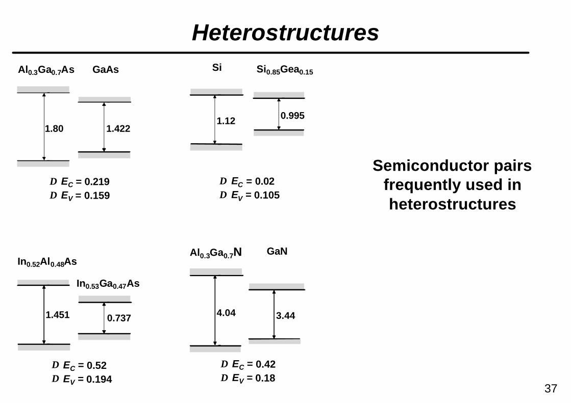
Semiconductor pairs frequently used in heterostructures
37
Al0.3Ga0.7As GaAs
1.80 1.422
Si0.85Gea0.15Si
0.9951.12
In0.52Al0.48As
In0.53Ga0.47As
Al0.3Ga0.7N GaN
1.451 0.737 4.04 3.44
∆ EC = 0.219∆ EV = 0.159
∆ EC = 0.02∆ EV = 0.105
∆ EC = 0.52∆ EV = 0.194
∆ EC = 0.42∆ EV = 0.18
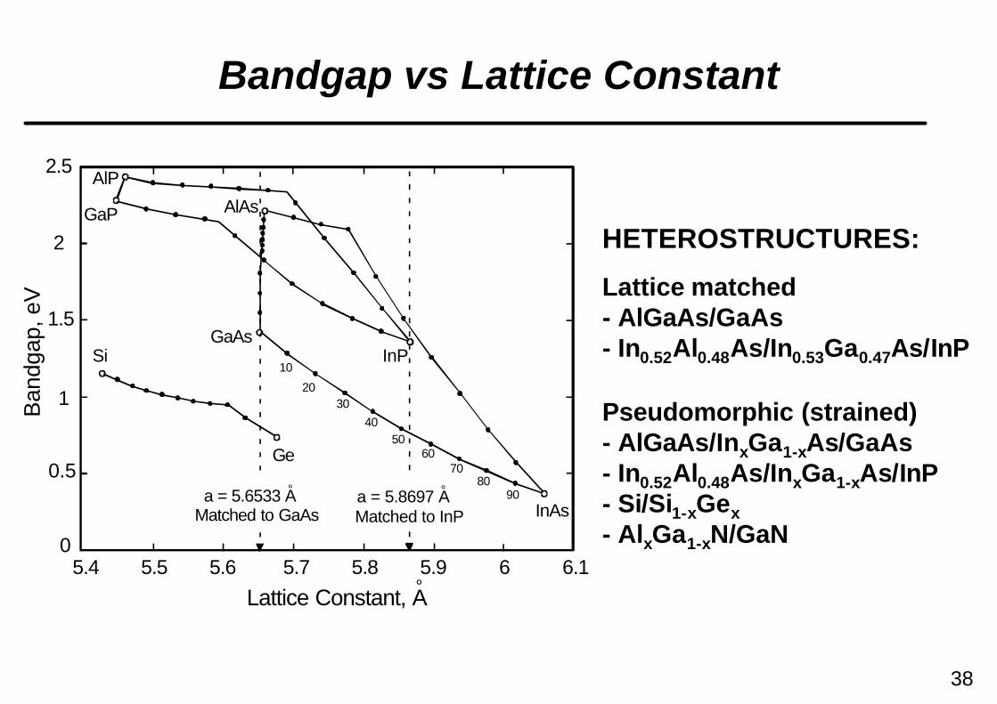
Bandgap vs Lattice Constant
HETEROSTRUCTURES:
Lattice matched- AlGaAs/GaAs- In0.52Al0.48As/In0.53Ga0.47As/InP
Pseudomorphic (strained)- AlGaAs/InxGa1-xAs/GaAs- In0.52Al0.48As/InxGa1-xAs/InP- Si/Si1-xGex- AlxGa1-xN/GaN
5.4 5.5 5.6 5.7 5.8 5.9 6 6.1
Lattice Constant, A
Ban
dgap
, eV
Si
Ge
GaAs
GaP
AlP
AlAs
InAs
InP10
2030
4050
6070
8090 a = 5.6533 A
Matched to GaAs
°
a = 5.8697 A Matched to InP
°°
2.5
2
1.5
1
0.5
0
38
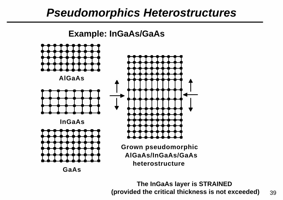
Pseudomorphics Heterostructures
AlGaAs
InGaAs
Grown pseudomorphic AlGaAs/InGaAs/GaAs heterostructure
GaAs
The InGaAs layer is STRAINED (provided the critical thickness is not exceeded) 39
Example: InGaAs/GaAs
Critical Thickness
0.0 0.2 0.4 0.6 0.8 1.01
10
100
1000
Empirical upper limit (AlGaN on GaN)
Empirical upper limit (InGaAs on GaAs)
Exp. AlGaN Exp. AlGaN Exp. InGaAs
Crit
ical
thic
knes
s, n
m
Composition x40
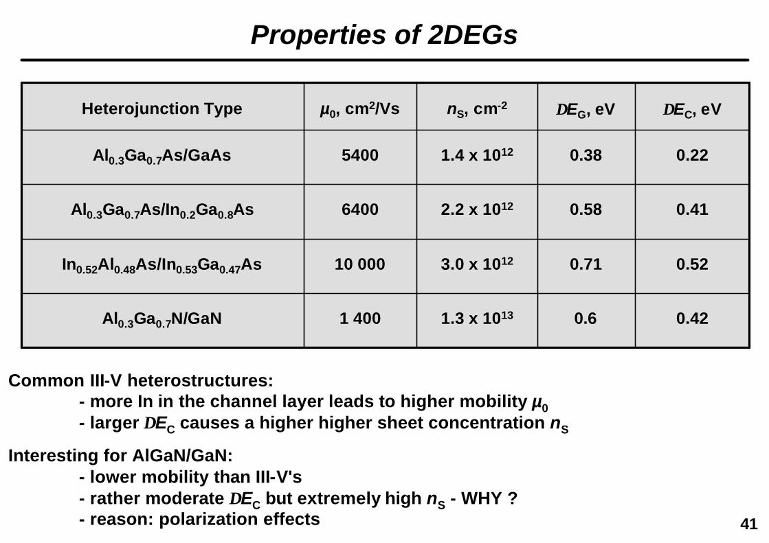
Properties of 2DEGs
1.3 x 10¹³
3.0 x 10¹²
2.2 x 10¹²
1.4 x 10¹²
nS, cm-2
0.420.61 400Al0.3Ga0.7N/GaN
0.520.7110 000In0.52Al0.48As/In0.53Ga0.47As
0.410.586400Al0.3Ga0.7As/In0.2Ga0.8As
0.220.385400Al0.3Ga0.7As/GaAs
∆EC, eV∆EG, eVµ0, cm2/VsHeterojunction Type
Common III-V heterostructures:- more In in the channel layer leads to higher mobility µ0- larger ∆EC causes a higher higher sheet concentration nS
Interesting for AlGaN/GaN:- lower mobility than III-V's- rather moderate ∆EC but extremely high nS - WHY ?- reason: polarization effects 41
Basics of RF Devices I
OUTLINE• Introduction • Mainstream Electronics vs. RF Electronics• Transistor Concepts I• RF Transistor Figures of Merit• Material Issues – Special Needs for RF• History and Evolution of RF Transistors
Frank Schwierz Technische Universität Ilmenau, Germany
TARGET Summer School, 13 September 2004Europa Beach, Crete 42
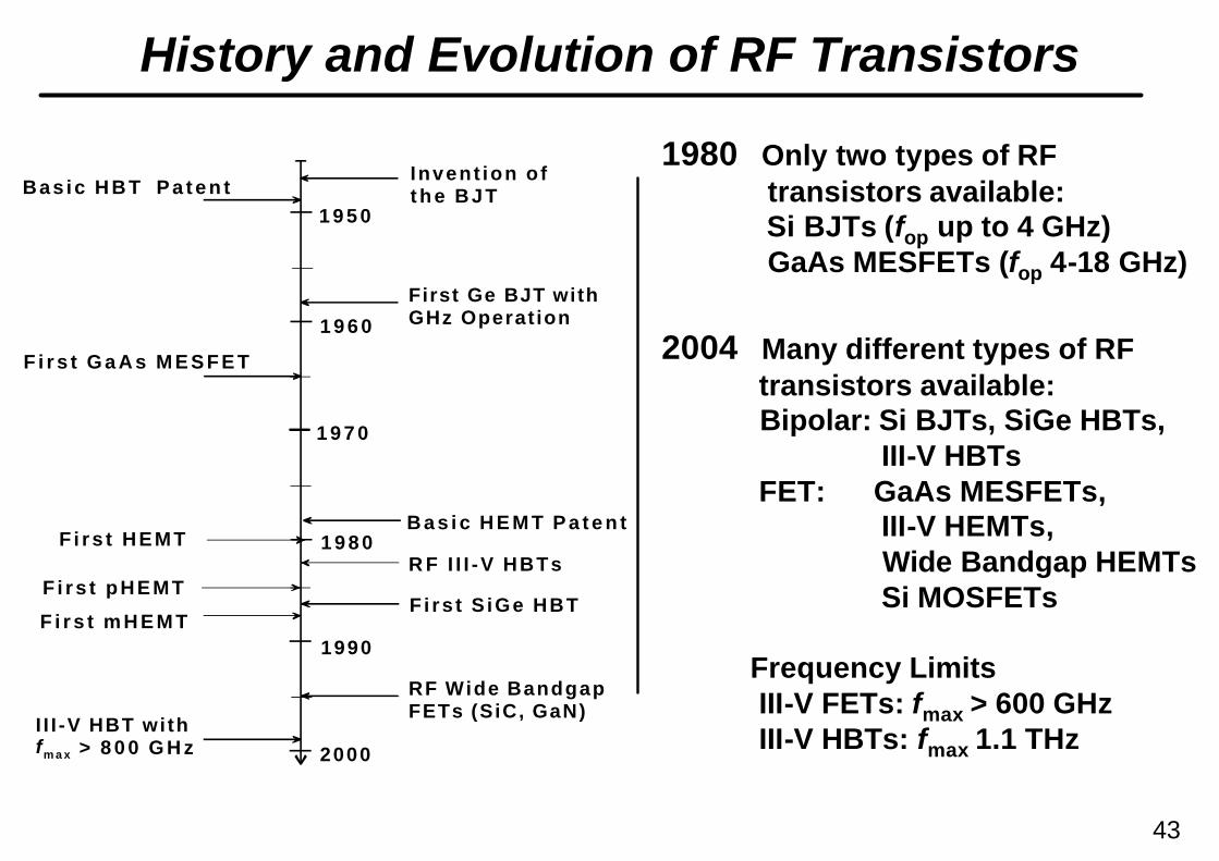
1 9 5 0
1 9 6 0
1 9 7 0
1 9 8 0
1990
2000
Invent ion ofthe BJT Bas ic H B T P a t e n t
F i r s t G a A s M E S F E T
B a s i c H E M T P a t e n tF i rs t HEMT
R F I I I -V HBTsF i rs t pHEMT
F i rs t S iGe HBTF i r s t m H E M T
II I -V HBT withfm a x > 8 0 0 G H z
First Ge BJT with GHz Operation
RF Wide BandgapFETs (SiC, GaN)
1980 Only two types of RFtransistors available:Si BJTs (fop up to 4 GHz)GaAs MESFETs (fop 4-18 GHz)
2004 Many different types of RF transistors available:Bipolar: Si BJTs, SiGe HBTs,
III-V HBTsFET: GaAs MESFETs,
III-V HEMTs,Wide Bandgap HEMTsSi MOSFETs
Frequency LimitsIII-V FETs: fmax > 600 GHzIII-V HBTs: fmax 1.1 THz
History and Evolution of RF Transistors
43
Important Trends:
• Continuous improvement of transistor performance - Continuous increase of the frequency limits fT and fmax
- Increase of the output power at a given frequency- Decrease of the minimum noise figure at a given frequency
• During the last 10 years: Shift of the applications of RF systems from defense and space applications to commercial mass markets- RF is becoming mainstream- Most commercial applications are in the lower GHz range
• Development of low-cost RF transistors for mass consumer markets.- Growing role of of Si-based RF transistors - For mass markets, cost is an extremely important issue – and Si technology is less expensive that any other semiconductor technology.
Trends in the Evolution of RF Transistors
44
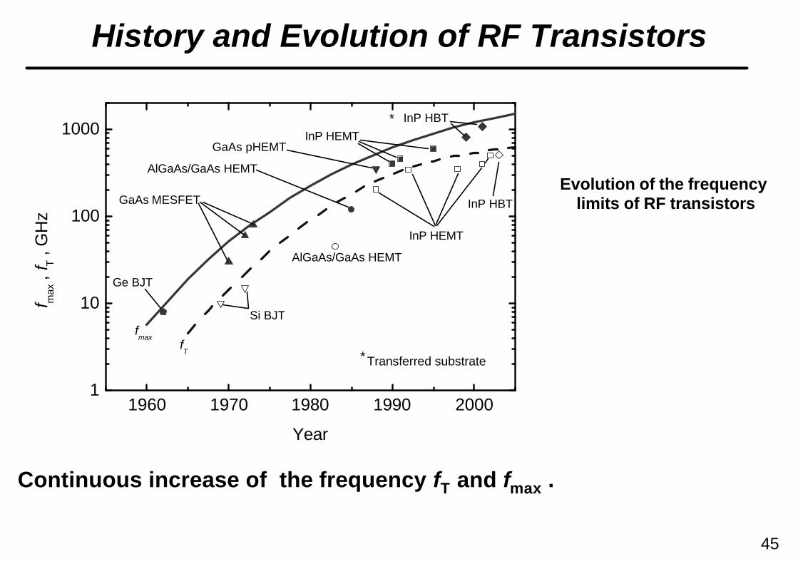
Continuous increase of the frequency fT and fmax .
History and Evolution of RF Transistors
45
1960 1970 1980 1990 20001
10
100
1000
InP HBT
*
*
Transferred substratefT
fmax
AlGaAs/GaAs HEMT
InP HEMT
Si BJT
AlGaAs/GaAs HEMT
GaAs pHEMTInP HEMT
InP HBT
GaAs MESFET
Ge BJT
f max
, f T
, G
Hz
Year
Evolution of the frequency limits of RF transistors
History and Evolution of RF Transistors
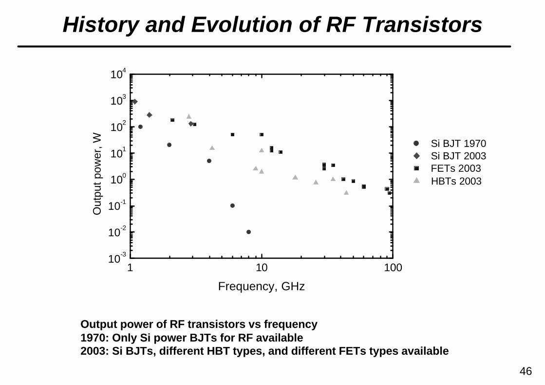
46
Output power of RF transistors vs frequency1970: Only Si power BJTs for RF available 2003: Si BJTs, different HBT types, and different FETs types available
1 10 10010-3
10-2
10-1
100
101
102
103
104
Si BJT 1970 Si BJT 2003 FETs 2003 HBTs 2003
Out
put p
ower
, W
Frequency, GHz
History and Evolution of RF Transistors
47
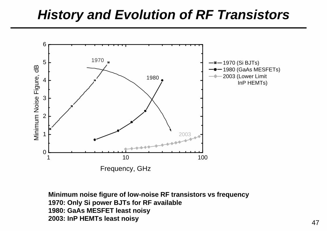
Minimum noise figure of low-noise RF transistors vs frequency1970: Only Si power BJTs for RF available1980: GaAs MESFET least noisy 2003: InP HEMTs least noisy
1 10 1000
1
2
3
4
5
6
2003
1980
1970
1970 (Si BJTs) 1980 (GaAs MESFETs) 2003 (Lower Limit
InP HEMTs)
Min
imum
Noi
se F
igur
e, d
B
Frequency, GHz