Embed Size (px)
Citation preview
A Microchip Technology Company
©2011 Silicon Storage Technology, Inc. S725081A 10/11
Data Sheet
www.microchip.com
Features• Single 2.7-3.6V Read and Write Operations
• Serial Interface Architecture– SPI Compatible: Mode 0 and Mode 3
• 33 MHz Max Clock Frequency
• Superior Reliability– Endurance: 100,000 Cycles (typical)– Greater than 100 years Data Retention
• Low Power Consumption:– Active Read Current: 7 mA (typical)– Standby Current: 8 µA (typical)
• Flexible Erase Capability– Uniform 4 KByte sectors– Uniform 32 KByte overlay blocks
• Fast Erase and Byte-Program:– Chip-Erase Time: 70 ms (typical)– Sector- or Block-Erase Time: 18 ms (typical)– Byte-Program Time: 14 µs (typical)
• Auto Address Increment (AAI) Programming– Decrease total chip programming time over Byte-Pro-
gram operations
• End-of-Write Detection– Software Status
• Hold Pin (HOLD#)– Suspends a serial sequence to the memory
without deselecting the device
• Write Protection (WP#)– Enables/Disables the Lock-Down function of the status
register
• Software Write Protection– Write protection through Block-Protection bits in status
register
• Temperature Range– Commercial: 0°C to +70°C– Industrial: -40°C to +85°C– Extended: -20°C to +85°C
• Packages Available– 8-lead SOIC 150 mil body width– 8-contact WSON (5mm x 6mm)
• All non-Pb (lead-free) devices are RoHS compliant
1 Mbit SPI Serial FlashSST25VF010A
SST's serial flash family features a four-wire, SPI-compatible interface that allowsfor a low pin-count package occupying less board space and ultimately loweringtotal system costs. SST25VF010A SPI serial flash memory is manufactured withSST proprietary, high performance CMOS SuperFlash Technology. The split-gatecell design and thick-oxide tunneling injector attain better reliability and manufac-turability compared with alternate approaches.
©20
1 Mbit SPI Serial FlashSST25VF010A
Data Sheet
A Microchip Technology Company
Product DescriptionSST’s serial flash family features a four-wire, SPI-compatible interface that allows for a low pin-count package occupying less board space and ultimately lowering total system costs.SST25VF010A SPI serial flash memory is manufactured with SST’s proprietary, high performanceCMOS SuperFlash Technology. The split-gate cell design and thick-oxide tunneling injector attainbetter reliability and manufacturability compared with alternate approaches.
The SST25VF010A device significantly improves performance, while lowering power consumption.The total energy consumed is a function of the applied voltage, current, and time of application.Since for any given voltage range, the SuperFlash technology uses less current to program andhas a shorter erase time, the total energy consumed during any Erase or Program operation isless than alternative flash memory technologies. The SST25VF010A device operates with a single2.7-3.6V power supply.
The SST25VF010A device is offered in both 8-lead SOIC and 8-contact WSON packages. See Figure1 for the pin assignments.
11 Silicon Storage Technology, Inc. S725081A 10/11
2
©20
1 Mbit SPI Serial FlashSST25VF010A
Data Sheet
A Microchip Technology Company
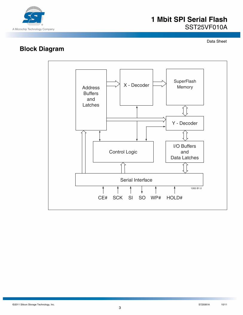
Block Diagram
1265 B1.0
I/O Buffersand
Data Latches
SuperFlashMemoryX - Decoder
Control Logic
AddressBuffers
andLatches
CE#
Y - Decoder
SCK SI SO WP# HOLD#
Serial Interface
11 Silicon Storage Technology, Inc. S725081A 10/11
3
©20
1 Mbit SPI Serial FlashSST25VF010A
Data Sheet
A Microchip Technology Company
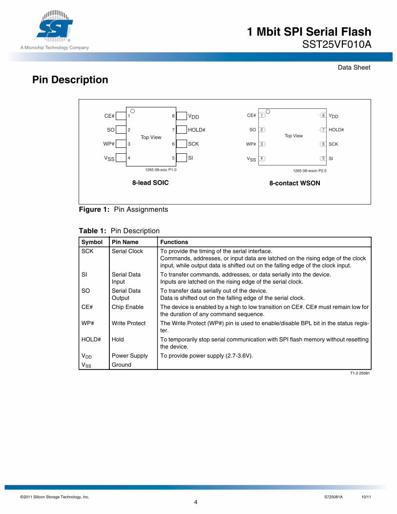
Pin Description
Figure 1: Pin Assignments
Table 1: Pin Description
Symbol Pin Name Functions
SCK Serial Clock To provide the timing of the serial interface.Commands, addresses, or input data are latched on the rising edge of the clockinput, while output data is shifted out on the falling edge of the clock input.
SI Serial DataInput
To transfer commands, addresses, or data serially into the device.Inputs are latched on the rising edge of the serial clock.
SO Serial DataOutput
To transfer data serially out of the device.Data is shifted out on the falling edge of the serial clock.
CE# Chip Enable The device is enabled by a high to low transition on CE#. CE# must remain low forthe duration of any command sequence.
WP# Write Protect The Write Protect (WP#) pin is used to enable/disable BPL bit in the status regis-ter.
HOLD# Hold To temporarily stop serial communication with SPI flash memory without resettingthe device.
VDD Power Supply To provide power supply (2.7-3.6V).
VSS GroundT1.0 25081
1
2
3
4
8
7
6
5
CE#
SO
WP#
VSS
VDD
HOLD#
SCK
SI
Top View
1265 08-soic P1.0
8-lead SOIC 8-contact WSON
1
2
3
4
8
7
6
5
CE#
SO
WP#
VSS
Top View
VDD
HOLD#
SCK
SI
1265 08-wson P2.0
11 Silicon Storage Technology, Inc. S725081A 10/11
4
©20
1 Mbit SPI Serial FlashSST25VF010A
Data Sheet
A Microchip Technology Company
Product Identification
Memory OrganizationThe SST25VF010A SuperFlash memory array is organized in 4 KByte sectors with 32 KByte overlayblocks.
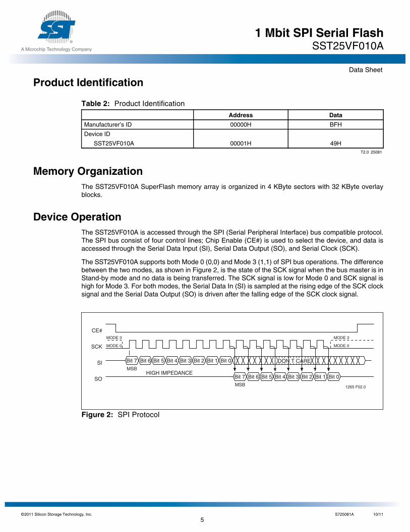
Device OperationThe SST25VF010A is accessed through the SPI (Serial Peripheral Interface) bus compatible protocol.The SPI bus consist of four control lines; Chip Enable (CE#) is used to select the device, and data isaccessed through the Serial Data Input (SI), Serial Data Output (SO), and Serial Clock (SCK).
The SST25VF010A supports both Mode 0 (0,0) and Mode 3 (1,1) of SPI bus operations. The differencebetween the two modes, as shown in Figure 2, is the state of the SCK signal when the bus master is inStand-by mode and no data is being transferred. The SCK signal is low for Mode 0 and SCK signal ishigh for Mode 3. For both modes, the Serial Data In (SI) is sampled at the rising edge of the SCK clocksignal and the Serial Data Output (SO) is driven after the falling edge of the SCK clock signal.
Figure 2: SPI Protocol
Table 2: Product Identification
Address Data
Manufacturer’s ID 00000H BFH
Device ID
SST25VF010A 00001H 49HT2.0 25081
1265 F02.0
MODE 3
SCK
SI
SO
CE#MODE 3
DON T CARE
Bit 7 Bit 6 Bit 5 Bit 4 Bit 3 Bit 2 Bit 1 Bit 0
Bit 7 Bit 6 Bit 5 Bit 4 Bit 3 Bit 2 Bit 1 Bit 0
MODE 0MODE 0
HIGH IMPEDANCEMSB
MSB
11 Silicon Storage Technology, Inc. S725081A 10/11
5
©20
1 Mbit SPI Serial FlashSST25VF010A
Data Sheet
A Microchip Technology Company
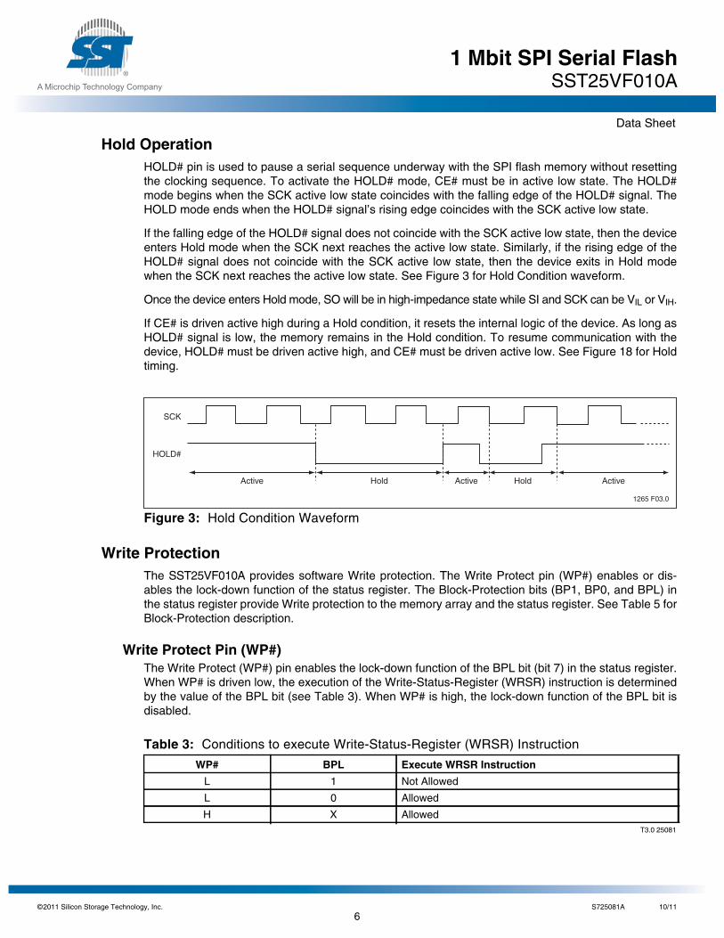
Hold OperationHOLD# pin is used to pause a serial sequence underway with the SPI flash memory without resettingthe clocking sequence. To activate the HOLD# mode, CE# must be in active low state. The HOLD#mode begins when the SCK active low state coincides with the falling edge of the HOLD# signal. TheHOLD mode ends when the HOLD# signal’s rising edge coincides with the SCK active low state.
If the falling edge of the HOLD# signal does not coincide with the SCK active low state, then the deviceenters Hold mode when the SCK next reaches the active low state. Similarly, if the rising edge of theHOLD# signal does not coincide with the SCK active low state, then the device exits in Hold modewhen the SCK next reaches the active low state. See Figure 3 for Hold Condition waveform.
Once the device enters Hold mode, SO will be in high-impedance state while SI and SCK can be VIL or VIH.
If CE# is driven active high during a Hold condition, it resets the internal logic of the device. As long asHOLD# signal is low, the memory remains in the Hold condition. To resume communication with thedevice, HOLD# must be driven active high, and CE# must be driven active low. See Figure 18 for Holdtiming.
Figure 3: Hold Condition Waveform
Write ProtectionThe SST25VF010A provides software Write protection. The Write Protect pin (WP#) enables or dis-ables the lock-down function of the status register. The Block-Protection bits (BP1, BP0, and BPL) inthe status register provide Write protection to the memory array and the status register. See Table 5 forBlock-Protection description.
Write Protect Pin (WP#)The Write Protect (WP#) pin enables the lock-down function of the BPL bit (bit 7) in the status register.When WP# is driven low, the execution of the Write-Status-Register (WRSR) instruction is determinedby the value of the BPL bit (see Table 3). When WP# is high, the lock-down function of the BPL bit isdisabled.
Table 3: Conditions to execute Write-Status-Register (WRSR) Instruction
WP# BPL Execute WRSR Instruction
L 1 Not Allowed
L 0 Allowed
H X AllowedT3.0 25081
Active Hold Active Hold Active
1265 F03.0
SCK
HOLD#
11 Silicon Storage Technology, Inc. S725081A 10/11
6
©20
1 Mbit SPI Serial FlashSST25VF010A
Data Sheet
A Microchip Technology Company
Status RegisterThe software status register provides status on whether the flash memory array is available for anyRead or Write operation, whether the device is Write enabled, and the state of the memory Write pro-tection. During an internal Erase or Program operation, the status register may be read only to deter-mine the completion of an operation in progress. Table 4 describes the function of each bit in thesoftware status register.
BusyThe Busy bit determines whether there is an internal Erase or Program operation in progress. A “1” forthe Busy bit indicates the device is busy with an operation in progress. A “0” indicates the device isready for the next valid operation.
Write Enable Latch (WEL)The Write-Enable-Latch bit indicates the status of the internal memory Write Enable Latch. If theWrite-Enable-Latch bit is set to “1”, it indicates the device is Write enabled. If the bit is set to “0” (reset),it indicates the device is not Write enabled and does not accept any memory Write (Program/Erase)commands. The Write-Enable-Latch bit is automatically reset under the following conditions:
• Power-up• Write-Disable (WRDI) instruction completion• Byte-Program instruction completion• Auto Address Increment (AAI) programming reached its highest memory address• Sector-Erase instruction completion• Block-Erase instruction completion• Chip-Erase instruction completion
Table 4: Software Status Register
Bit Name FunctionDefault atPower-up Read/Write
0 BUSY 1 = Internal Write operation is in progress0 = No internal Write operation is in progress
0 R
1 WEL 1 = Device is memory Write enabled0 = Device is not memory Write enabled
0 R
2 BP0 Indicate current level of block write protection (See Table 5) 1 R/W
3 BP1 Indicate current level of block write protection (See Table 5) 1 R/W
4:5 RES Reserved for future use 0 N/A
6 AAI Auto Address Increment Programming status1 = AAI programming mode0 = Byte-Program mode
0 R
7 BPL 1 = BP1, BP0 are read-only bits0 = BP1, BP0 are read/writable
0 R/W
T4.0 25081
11 Silicon Storage Technology, Inc. S725081A 10/11
7
©20
1 Mbit SPI Serial FlashSST25VF010A
Data Sheet
A Microchip Technology Company
Block Protection (BP1, BP0)The Block-Protection (BP1, BP0) bits define the size of the memory area, as defined in Table 5, to besoftware protected against any memory Write (Program or Erase) operations. The Write-Status-Regis-ter (WRSR) instruction is used to program the BP1 and BP0 bits as long as WP# is high or the Block-Protect-Lock (BPL) bit is 0. Chip-Erase can only be executed if Block-Protection bits are both 0. Afterpower-up, BP1 and BP0 are set to 1.
Block Protection Lock-Down (BPL)WP# pin driven low (VIL), enables the Block-Protection-Lock-Down (BPL) bit. When BPL is set to 1, itprevents any further alteration of the BPL, BP1, and BP0 bits. When the WP# pin is driven high (VIH),the BPL bit has no effect and its value is “Don’t Care”. After power-up, the BPL bit is reset to 0.
Auto Address Increment (AAI)The Auto Address Increment Programming-Status bit provides status on whether the device is in AAIprogramming mode or Byte-Program mode. The default at power up is Byte-Program mode.
Table 5: Software Status RegisterBlock Protection1
1. Default at power-up for BP1 and BP0 is ‘11’.
Protection Level
StatusRegister Bit Protected
Memory AreaBP1 BP0
0 0 0 None
1 (1/4 Memory Array) 0 1 018000H-01FFFFH
2 (1/2 Memory Array) 1 0 010000H-01FFFFH
3 (Full Memory Array) 1 1 000000H-01FFFFHT5.0 25081
11 Silicon Storage Technology, Inc. S725081A 10/11
8
©20
1 Mbit SPI Serial FlashSST25VF010A
Data Sheet
A Microchip Technology Company
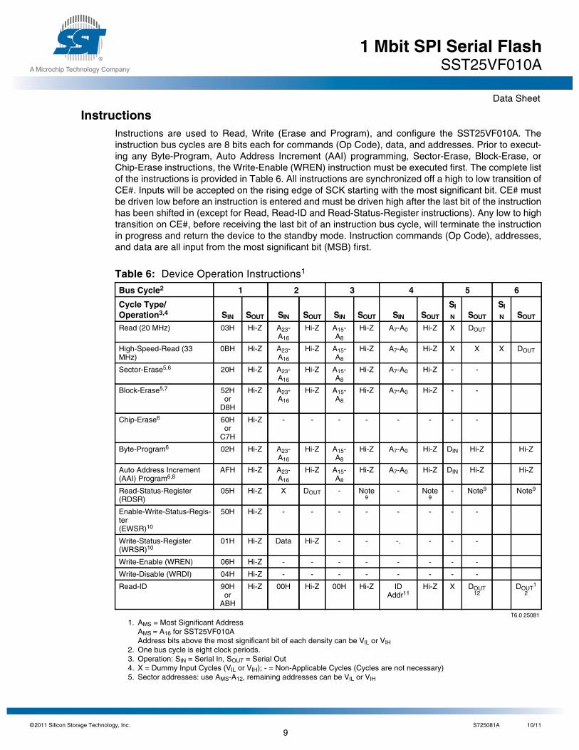
InstructionsInstructions are used to Read, Write (Erase and Program), and configure the SST25VF010A. Theinstruction bus cycles are 8 bits each for commands (Op Code), data, and addresses. Prior to execut-ing any Byte-Program, Auto Address Increment (AAI) programming, Sector-Erase, Block-Erase, orChip-Erase instructions, the Write-Enable (WREN) instruction must be executed first. The complete listof the instructions is provided in Table 6. All instructions are synchronized off a high to low transition ofCE#. Inputs will be accepted on the rising edge of SCK starting with the most significant bit. CE# mustbe driven low before an instruction is entered and must be driven high after the last bit of the instructionhas been shifted in (except for Read, Read-ID and Read-Status-Register instructions). Any low to hightransition on CE#, before receiving the last bit of an instruction bus cycle, will terminate the instructionin progress and return the device to the standby mode. Instruction commands (Op Code), addresses,and data are all input from the most significant bit (MSB) first.
Table 6: Device Operation Instructions1
1. AMS = Most Significant AddressAMS = A16 for SST25VF010AAddress bits above the most significant bit of each density can be VIL or VIH
Bus Cycle2
2. One bus cycle is eight clock periods.
1 2 3 4 5 6
Cycle Type/Operation3,4
3. Operation: SIN = Serial In, SOUT = Serial Out4. X = Dummy Input Cycles (VIL or VIH); - = Non-Applicable Cycles (Cycles are not necessary)
SIN SOUT SIN SOUT SIN SOUT SIN SOUT
SI
N SOUT
SI
N SOUT
Read (20 MHz) 03H Hi-Z A23-A16
Hi-Z A15-A8
Hi-Z A7-A0 Hi-Z X DOUT
High-Speed-Read (33MHz)
0BH Hi-Z A23-A16
Hi-Z A15-A8
Hi-Z A7-A0 Hi-Z X X X DOUT
Sector-Erase5,6
5. Sector addresses: use AMS-A12, remaining addresses can be VIL or VIH
20H Hi-Z A23-A16
Hi-Z A15-A8
Hi-Z A7-A0 Hi-Z - -
Block-Erase5,7 52Hor
D8H
Hi-Z A23-A16
Hi-Z A15-A8
Hi-Z A7-A0 Hi-Z - -
Chip-Erase6 60Hor
C7H
Hi-Z - - - - - - - -
Byte-Program6 02H Hi-Z A23-A16
Hi-Z A15-A8
Hi-Z A7-A0 Hi-Z DIN Hi-Z Hi-Z
Auto Address Increment(AAI) Program6,8
AFH Hi-Z A23-A16
Hi-Z A15-A8
Hi-Z A7-A0 Hi-Z DIN Hi-Z Hi-Z
Read-Status-Register(RDSR)
05H Hi-Z X DOUT - Note9
- Note9
- Note9 Note9
Enable-Write-Status-Regis-ter(EWSR)10
50H Hi-Z - - - - - - - -
Write-Status-Register(WRSR)10
01H Hi-Z Data Hi-Z - - -. - - -
Write-Enable (WREN) 06H Hi-Z - - - - - - - -
Write-Disable (WRDI) 04H Hi-Z - - - - - - - -
Read-ID 90Hor
ABH
Hi-Z 00H Hi-Z 00H Hi-Z IDAddr11
Hi-Z X DOUT12
DOUT1
2
T6.0 25081
11 Silicon Storage Technology, Inc. S725081A 10/11
9
©20
1 Mbit SPI Serial FlashSST25VF010A
Data Sheet
A Microchip Technology Company
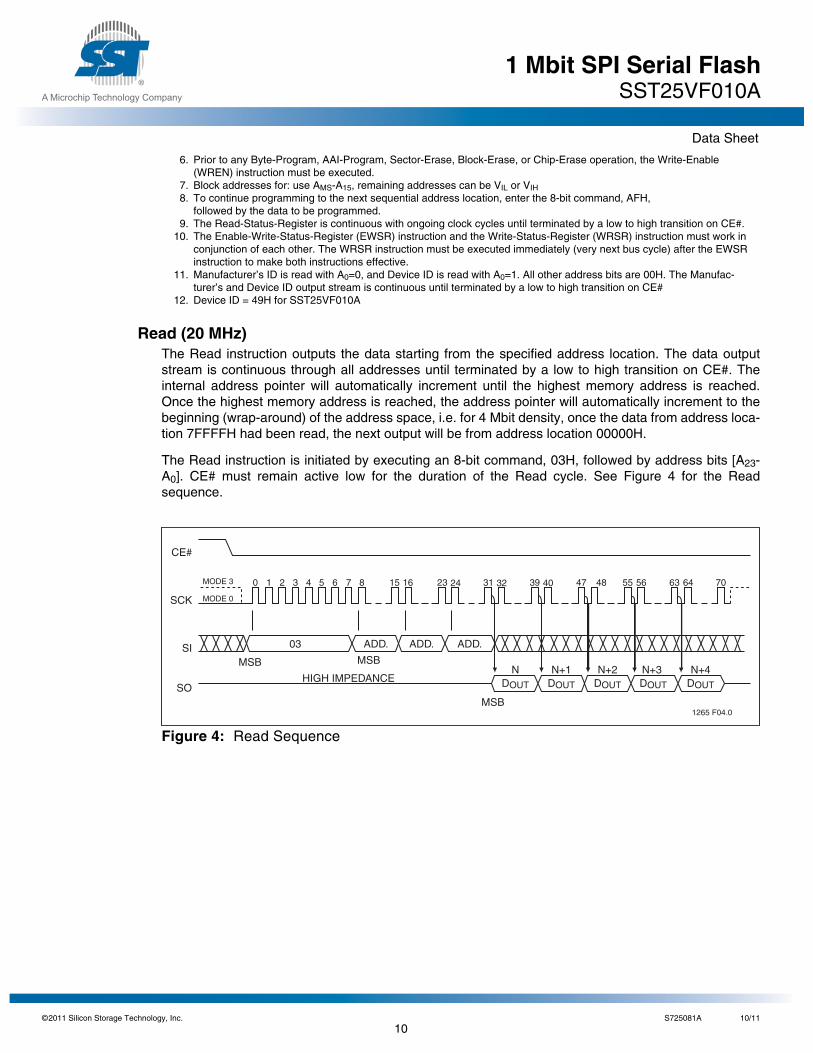
Read (20 MHz)The Read instruction outputs the data starting from the specified address location. The data outputstream is continuous through all addresses until terminated by a low to high transition on CE#. Theinternal address pointer will automatically increment until the highest memory address is reached.Once the highest memory address is reached, the address pointer will automatically increment to thebeginning (wrap-around) of the address space, i.e. for 4 Mbit density, once the data from address loca-tion 7FFFFH had been read, the next output will be from address location 00000H.
The Read instruction is initiated by executing an 8-bit command, 03H, followed by address bits [A23-A0]. CE# must remain active low for the duration of the Read cycle. See Figure 4 for the Readsequence.
Figure 4: Read Sequence
6. Prior to any Byte-Program, AAI-Program, Sector-Erase, Block-Erase, or Chip-Erase operation, the Write-Enable(WREN) instruction must be executed.
7. Block addresses for: use AMS-A15, remaining addresses can be VIL or VIH8. To continue programming to the next sequential address location, enter the 8-bit command, AFH,
followed by the data to be programmed.9. The Read-Status-Register is continuous with ongoing clock cycles until terminated by a low to high transition on CE#.
10. The Enable-Write-Status-Register (EWSR) instruction and the Write-Status-Register (WRSR) instruction must work inconjunction of each other. The WRSR instruction must be executed immediately (very next bus cycle) after the EWSRinstruction to make both instructions effective.
11. Manufacturer’s ID is read with A0=0, and Device ID is read with A0=1. All other address bits are 00H. The Manufac-turer’s and Device ID output stream is continuous until terminated by a low to high transition on CE#
12. Device ID = 49H for SST25VF010A
1265 F04.0
CE#
SO
SI
SCK
ADD.
0 1 2 3 4 5 6 7 8
ADD. ADD.03
HIGH IMPEDANCE
15 16 23 24 31 32 39 40 7047 48 55 56 63 64
N+2 N+3 N+4N N+1DOUT
MSB MSB
MSB
MODE 0
MODE 3
DOUT DOUT DOUT DOUT
11 Silicon Storage Technology, Inc. S725081A 10/11
10
©20
1 Mbit SPI Serial FlashSST25VF010A
Data Sheet
A Microchip Technology Company
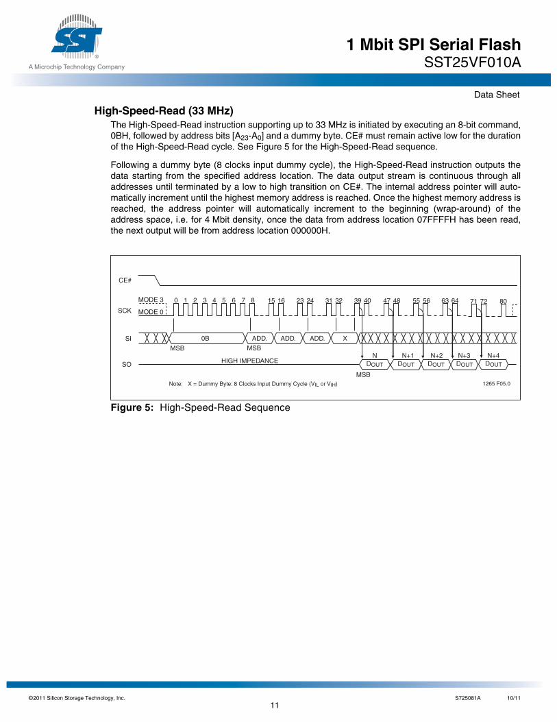
High-Speed-Read (33 MHz)The High-Speed-Read instruction supporting up to 33 MHz is initiated by executing an 8-bit command,0BH, followed by address bits [A23-A0] and a dummy byte. CE# must remain active low for the durationof the High-Speed-Read cycle. See Figure 5 for the High-Speed-Read sequence.
Following a dummy byte (8 clocks input dummy cycle), the High-Speed-Read instruction outputs thedata starting from the specified address location. The data output stream is continuous through alladdresses until terminated by a low to high transition on CE#. The internal address pointer will auto-matically increment until the highest memory address is reached. Once the highest memory address isreached, the address pointer will automatically increment to the beginning (wrap-around) of theaddress space, i.e. for 4 Mbit density, once the data from address location 07FFFFH has been read,the next output will be from address location 000000H.
Figure 5: High-Speed-Read Sequence
1265 F05.0
CE#
SO
SI
SCK
ADD.
0 1 2 3 4 5 6 7 8
ADD. ADD.0B
HIGH IMPEDANCE
15 16 23 24 31 32 39 40 47 48 55 56 63 64
N+2 N+3 N+4N N+1
X
MSB
MSBMSB
MODE 0
MODE 3
DOUT DOUT DOUT DOUT
8071 72
DOUT
Note: X = Dummy Byte: 8 Clocks Input Dummy Cycle (VIL or VIH)
11 Silicon Storage Technology, Inc. S725081A 10/11
11
©20
1 Mbit SPI Serial FlashSST25VF010A
Data Sheet
A Microchip Technology Company
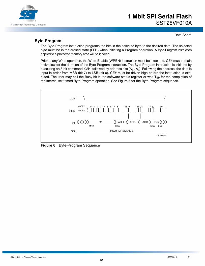
Byte-ProgramThe Byte-Program instruction programs the bits in the selected byte to the desired data. The selectedbyte must be in the erased state (FFH) when initiating a Program operation. A Byte-Program instructionapplied to a protected memory area will be ignored.
Prior to any Write operation, the Write-Enable (WREN) instruction must be executed. CE# must remainactive low for the duration of the Byte-Program instruction. The Byte-Program instruction is initiated byexecuting an 8-bit command, 02H, followed by address bits [A23-A0]. Following the address, the data isinput in order from MSB (bit 7) to LSB (bit 0). CE# must be driven high before the instruction is exe-cuted. The user may poll the Busy bit in the software status register or wait TBP for the completion ofthe internal self-timed Byte-Program operation. See Figure 6 for the Byte-Program sequence.
Figure 6: Byte-Program Sequence
1265 F06.0
CE#
SO
SI
SCK
ADD.
0 1 2 3 4 5 6 7 8
ADD. ADD. DIN02
HIGH IMPEDANCE
15 16 23 24 31 32 39
MODE 0
MODE 3
MSBMSBMSB LSB
11 Silicon Storage Technology, Inc. S725081A 10/11
12
©20
1 Mbit SPI Serial FlashSST25VF010A
Data Sheet
A Microchip Technology Company
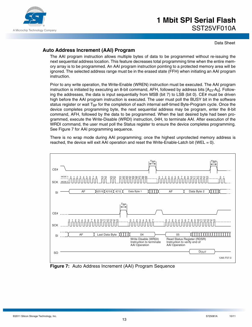
Auto Address Increment (AAI) ProgramThe AAI program instruction allows multiple bytes of data to be programmed without re-issuing thenext sequential address location. This feature decreases total programming time when the entire mem-ory array is to be programmed. An AAI program instruction pointing to a protected memory area will beignored. The selected address range must be in the erased state (FFH) when initiating an AAI programinstruction.
Prior to any write operation, the Write-Enable (WREN) instruction must be executed. The AAI programinstruction is initiated by executing an 8-bit command, AFH, followed by address bits [A23-A0]. Follow-ing the addresses, the data is input sequentially from MSB (bit 7) to LSB (bit 0). CE# must be drivenhigh before the AAI program instruction is executed. The user must poll the BUSY bit in the softwarestatus register or wait TBP for the completion of each internal self-timed Byte-Program cycle. Once thedevice completes programming byte, the next sequential address may be program, enter the 8-bitcommand, AFH, followed by the data to be programmed. When the last desired byte had been pro-grammed, execute the Write-Disable (WRDI) instruction, 04H, to terminate AAI. After execution of theWRDI command, the user must poll the Status register to ensure the device completes programming.See Figure 7 for AAI programming sequence.
There is no wrap mode during AAI programming; once the highest unprotected memory address isreached, the device will exit AAI operation and reset the Write-Enable-Latch bit (WEL = 0).
Figure 7: Auto Address Increment (AAI) Program Sequence
CE#
SI
SCK
A[23:16] A[15:8] A[7:0]AF Data Byte 1 AF Data Byte 2
CE#
SI
SO
SCK
Write Disable (WRDI)Instruction to terminateAAI Operation
Read Status Register (RDSR)Instruction to verify end ofAAI Operation
04Last Data ByteAF 05
DOUT
MODE 3
MODE 0
TBP TBP
TBP
1265 F07.0
0 1 2 3 4 5 6 7 8 32 33 34 35 36 37 38 3915 16 23 24 31 0 1 2 3 4 5 6 7 8 9 10 11 12 13 14 15 0 1
0 1 2 3 4 5 6 70 1 2 3 4 5 6 7 8 9 10 11 12 13 14 15 0 1 2 3 4 5 6 7 8 9 10 11 12 13 14 15
11 Silicon Storage Technology, Inc. S725081A 10/11
13
©20
1 Mbit SPI Serial FlashSST25VF010A
Data Sheet
A Microchip Technology Company
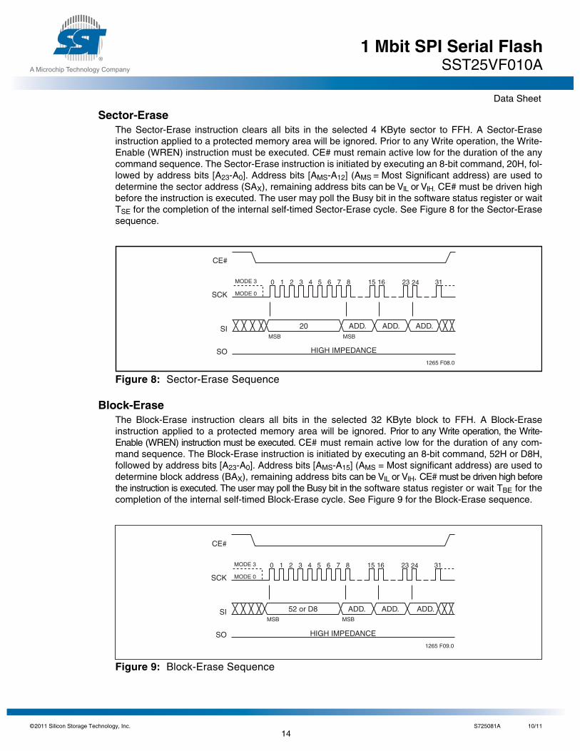
Sector-EraseThe Sector-Erase instruction clears all bits in the selected 4 KByte sector to FFH. A Sector-Eraseinstruction applied to a protected memory area will be ignored. Prior to any Write operation, the Write-Enable (WREN) instruction must be executed. CE# must remain active low for the duration of the anycommand sequence. The Sector-Erase instruction is initiated by executing an 8-bit command, 20H, fol-lowed by address bits [A23-A0]. Address bits [AMS-A12] (AMS = Most Significant address) are used todetermine the sector address (SAX), remaining address bits can be VIL or VIH. CE# must be driven highbefore the instruction is executed. The user may poll the Busy bit in the software status register or waitTSE for the completion of the internal self-timed Sector-Erase cycle. See Figure 8 for the Sector-Erasesequence.
Figure 8: Sector-Erase Sequence
Block-EraseThe Block-Erase instruction clears all bits in the selected 32 KByte block to FFH. A Block-Eraseinstruction applied to a protected memory area will be ignored. Prior to any Write operation, the Write-Enable (WREN) instruction must be executed. CE# must remain active low for the duration of any com-mand sequence. The Block-Erase instruction is initiated by executing an 8-bit command, 52H or D8H,followed by address bits [A23-A0]. Address bits [AMS-A15] (AMS = Most significant address) are used todetermine block address (BAX), remaining address bits can be VIL or VIH. CE# must be driven high beforethe instruction is executed. The user may poll the Busy bit in the software status register or wait TBE for thecompletion of the internal self-timed Block-Erase cycle. See Figure 9 for the Block-Erase sequence.
Figure 9: Block-Erase Sequence
CE#
SO
SI
SCK
ADD.
0 1 2 3 4 5 6 7 8
ADD. ADD.20
HIGH IMPEDANCE
15 16 23 24 31
MODE 0
MODE 3
1265 F08.0
MSBMSB
CE#
SO
SI
SCK
ADD.
0 1 2 3 4 5 6 7 8
ADD. ADD.52 or D8
HIGH IMPEDANCE
15 16 23 24 31
MODE 0
MODE 3
1265 F09.0
MSB MSB
11 Silicon Storage Technology, Inc. S725081A 10/11
14
©20
1 Mbit SPI Serial FlashSST25VF010A
Data Sheet
A Microchip Technology Company
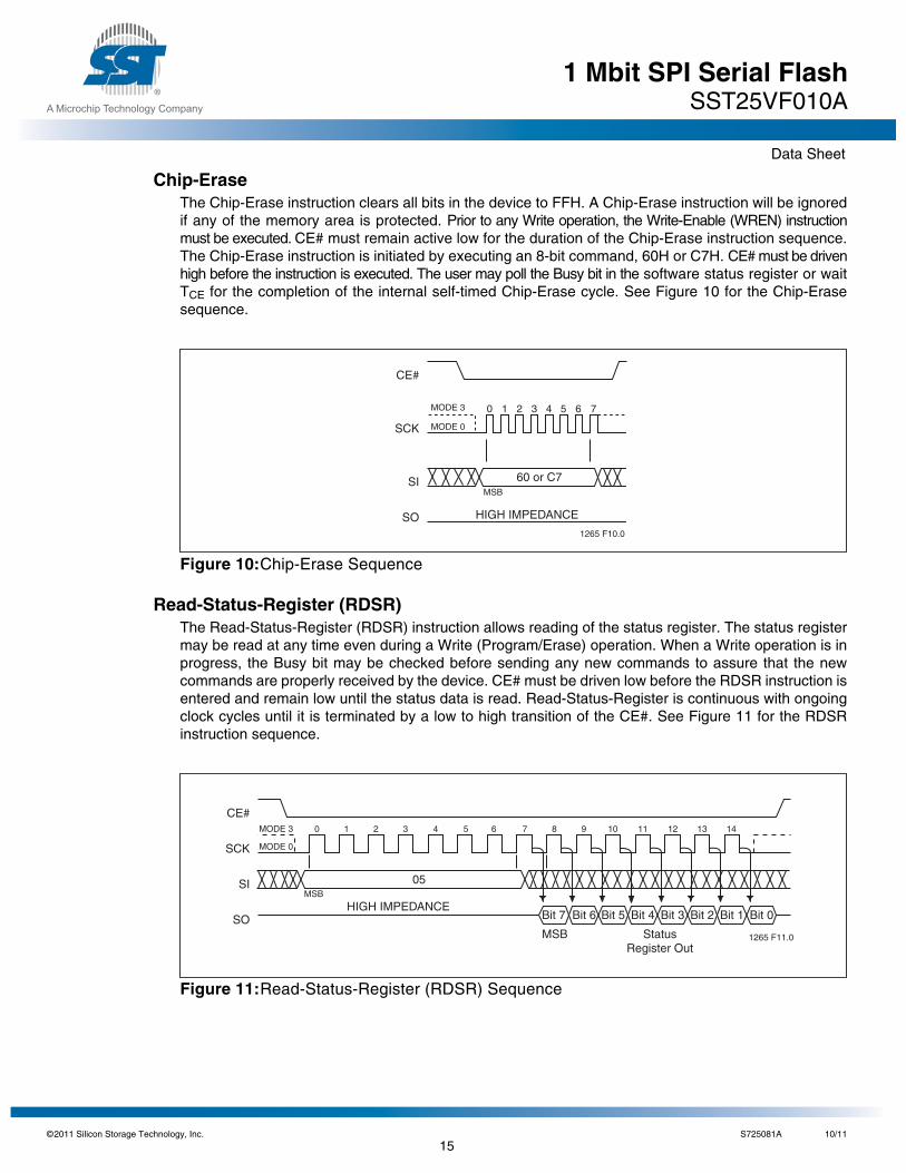
Chip-EraseThe Chip-Erase instruction clears all bits in the device to FFH. A Chip-Erase instruction will be ignoredif any of the memory area is protected. Prior to any Write operation, the Write-Enable (WREN) instructionmust be executed. CE# must remain active low for the duration of the Chip-Erase instruction sequence.The Chip-Erase instruction is initiated by executing an 8-bit command, 60H or C7H. CE# must be drivenhigh before the instruction is executed. The user may poll the Busy bit in the software status register or waitTCE for the completion of the internal self-timed Chip-Erase cycle. See Figure 10 for the Chip-Erasesequence.
Figure 10:Chip-Erase Sequence
Read-Status-Register (RDSR)The Read-Status-Register (RDSR) instruction allows reading of the status register. The status registermay be read at any time even during a Write (Program/Erase) operation. When a Write operation is inprogress, the Busy bit may be checked before sending any new commands to assure that the newcommands are properly received by the device. CE# must be driven low before the RDSR instruction isentered and remain low until the status data is read. Read-Status-Register is continuous with ongoingclock cycles until it is terminated by a low to high transition of the CE#. See Figure 11 for the RDSRinstruction sequence.
Figure 11:Read-Status-Register (RDSR) Sequence
CE#
SO
SI
SCK
0 1 2 3 4 5 6 7
60 or C7
HIGH IMPEDANCE
MODE 0
MODE 3
1265 F10.0
MSB
0 1 2 3 4 5 6 7 8 9 10 11 12 13 14
1265 F11.0
MODE 3
SCK
SI
SO
CE#
Bit 7 Bit 6 Bit 5 Bit 4 Bit 3 Bit 2 Bit 1 Bit 0
05
MODE 0
HIGH IMPEDANCE
StatusRegister Out
MSB
MSB
11 Silicon Storage Technology, Inc. S725081A 10/11
15
©20
1 Mbit SPI Serial FlashSST25VF010A
Data Sheet
A Microchip Technology Company
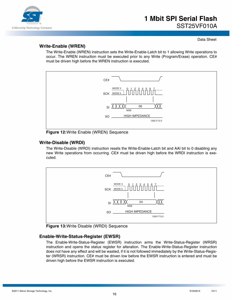
Write-Enable (WREN)The Write-Enable (WREN) instruction sets the Write-Enable-Latch bit to 1 allowing Write operations tooccur. The WREN instruction must be executed prior to any Write (Program/Erase) operation. CE#must be driven high before the WREN instruction is executed.
Figure 12:Write Enable (WREN) Sequence
Write-Disable (WRDI)The Write-Disable (WRDI) instruction resets the Write-Enable-Latch bit and AAI bit to 0 disabling anynew Write operations from occurring. CE# must be driven high before the WRDI instruction is exe-cuted.
Figure 13:Write Disable (WRDI) Sequence
Enable-Write-Status-Register (EWSR)The Enable-Write-Status-Register (EWSR) instruction arms the Write-Status-Register (WRSR)instruction and opens the status register for alteration. The Enable-Write-Status-Register instructiondoes not have any effect and will be wasted, if it is not followed immediately by the Write-Status-Regis-ter (WRSR) instruction. CE# must be driven low before the EWSR instruction is entered and must bedriven high before the EWSR instruction is executed.
CE#
SO
SI
SCK
0 1 2 3 4 5 6 7
06
HIGH IMPEDANCE
MODE 0
MODE 3
1265 F12.0
MSB
CE#
SO
SI
SCK
0 1 2 3 4 5 6 7
04
HIGH IMPEDANCE
MODE 0
MODE 3
1265 F13.0
MSB
11 Silicon Storage Technology, Inc. S725081A 10/11
16
©20
1 Mbit SPI Serial FlashSST25VF010A
Data Sheet
A Microchip Technology Company
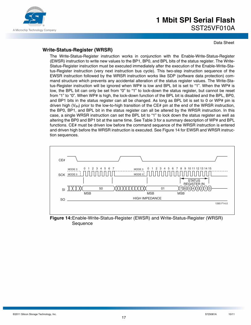
Write-Status-Register (WRSR)The Write-Status-Register instruction works in conjunction with the Enable-Write-Status-Register(EWSR) instruction to write new values to the BP1, BP0, and BPL bits of the status register. The Write-Status-Register instruction must be executed immediately after the execution of the Enable-Write-Sta-tus-Register instruction (very next instruction bus cycle). This two-step instruction sequence of theEWSR instruction followed by the WRSR instruction works like SDP (software data protection) com-mand structure which prevents any accidental alteration of the status register values. The Write-Sta-tus-Register instruction will be ignored when WP# is low and BPL bit is set to “1”. When the WP# islow, the BPL bit can only be set from “0” to “1” to lock-down the status register, but cannot be resetfrom “1” to “0”. When WP# is high, the lock-down function of the BPL bit is disabled and the BPL, BP0,and BP1 bits in the status register can all be changed. As long as BPL bit is set to 0 or WP# pin isdriven high (VIH) prior to the low-to-high transition of the CE# pin at the end of the WRSR instruction,the BP0, BP1, and BPL bit in the status register can all be altered by the WRSR instruction. In thiscase, a single WRSR instruction can set the BPL bit to “1” to lock down the status register as well asaltering the BP0 and BP1 bit at the same time. See Table 3 for a summary description of WP# and BPLfunctions. CE# must be driven low before the command sequence of the WRSR instruction is enteredand driven high before the WRSR instruction is executed. See Figure 14 for EWSR and WRSR instruc-tion sequences.
Figure 14:Enable-Write-Status-Register (EWSR) and Write-Status-Register (WRSR)Sequence
1265 F14.0
MODE 3
HIGH IMPEDANCE
MODE 0
STATUSREGISTER IN
7 6 5 4 3 2 1 0
MSBMSBMSB
01
MODE 3
SCK
SI
SO
CE#
MODE 0
50
0 1 2 3 4 5 6 7 0 1 2 3 4 5 6 7 8 9 10 11 12 13 14 15
11 Silicon Storage Technology, Inc. S725081A 10/11
17
©20
1 Mbit SPI Serial FlashSST25VF010A
Data Sheet
A Microchip Technology Company
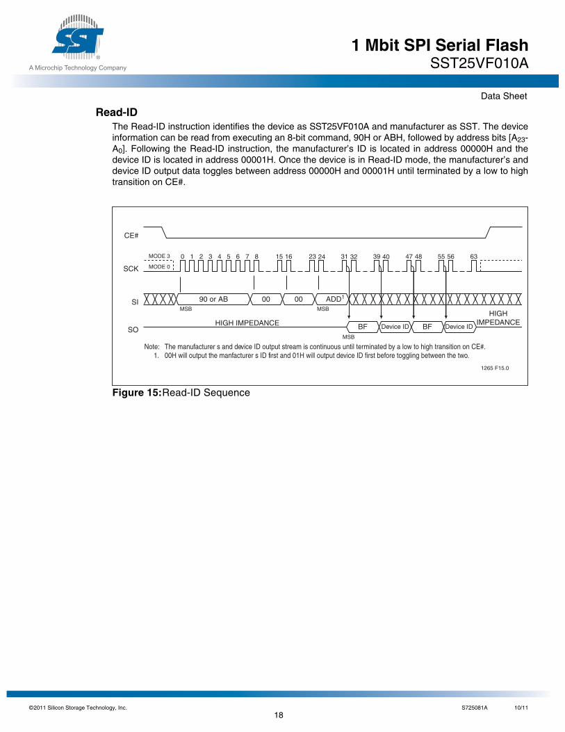
Read-IDThe Read-ID instruction identifies the device as SST25VF010A and manufacturer as SST. The deviceinformation can be read from executing an 8-bit command, 90H or ABH, followed by address bits [A23-A0]. Following the Read-ID instruction, the manufacturer’s ID is located in address 00000H and thedevice ID is located in address 00001H. Once the device is in Read-ID mode, the manufacturer’s anddevice ID output data toggles between address 00000H and 00001H until terminated by a low to hightransition on CE#.
Figure 15:Read-ID Sequence
1265 F15.0
CE#
SO
SI
SCK
00
0 1 2 3 4 5 6 7 8
00 ADD190 or AB
HIGH IMPEDANCE
15 16 23 24 31 32 39 40 47 48 55 56 63
BF Device ID BF Device ID
Note: The manufacturer s and device ID output stream is continuous until terminated by a low to high transition on CE#.1. 00H will output the manfacturer s ID first and 01H will output device ID first before toggling between the two.
HIGHIMPEDANCE
MODE 3
MODE 0
MSB MSB
MSB
11 Silicon Storage Technology, Inc. S725081A 10/11
18
©20
1 Mbit SPI Serial FlashSST25VF010A
Data Sheet
A Microchip Technology Company
Electrical Specifications
Absolute Maximum Stress Ratings (Applied conditions greater than those listed under “AbsoluteMaximum Stress Ratings” may cause permanent damage to the device. This is a stress rating only andfunctional operation of the device at these conditions or conditions greater than those defined in theoperational sections of this data sheet is not implied. Exposure to absolute maximum stress rating con-ditions may affect device reliability.)
Temperature Under Bias . . . . . . . . . . . . . . . . . . . . . . . . . . . . . . . . . . . . . . . . . . . . . . -55°C to +125°CStorage Temperature. . . . . . . . . . . . . . . . . . . . . . . . . . . . . . . . . . . . . . . . . . . . . . . . . -65°C to +150°CD. C. Voltage on Any Pin to Ground Potential . . . . . . . . . . . . . . . . . . . . . . . . . . . . . -0.5V to VDD+0.5VTransient Voltage (<20 ns) on Any Pin to Ground Potential . . . . . . . . . . . . . . . . . . -2.0V to VDD+2.0VPackage Power Dissipation Capability (TA = 25°C). . . . . . . . . . . . . . . . . . . . . . . . . . . . . . . . . . . 1.0WSurface Mount Solder Reflow Temperature . . . . . . . . . . . . . . . . . . . . . . . . . . . 260°C for 10 secondsOutput Short Circuit Current1. . . . . . . . . . . . . . . . . . . . . . . . . . . . . . . . . . . . . . . . . . . . . . . . . . . 50 mA
1. Output shorted for no more than one second. No more than one output shorted at a time.
Table 7: Operating Range
Range Ambient Temp VDD
Commercial 0°C to +70°C 2.7-3.6V
Industrial -40°C to +85°C 2.7-3.6V
Extended -20°C to +85°C 2.7-3.6VT7.1 25081
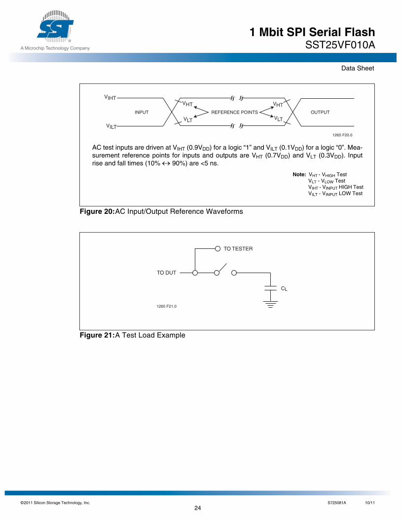
Table 8: AC Conditions of Test1
1. See Figures 20 and 21
Input Rise/Fall Time Output Load
5ns CL = 30 pFT8.1 25081
Table 9: DC Operating Characteristics VDD = 2.7-3.6V
Symbol Parameter
Limits
Test ConditionsMin Max Units
IDDR Read Current 10 mA CE#=0.1 VDD/0.9 VDD@20 MHz, SO=open
IDDW Program and Erase Current 30 mA CE#=VDD
ISB Standby Current 15 µA CE#=VDD, VIN=VDD or VSS
ILI Input Leakage Current 1 µA VIN=GND to VDD, VDD=VDD Max
ILO Output Leakage Current 1 µA VOUT=GND to VDD, VDD=VDD Max
VIL Input Low Voltage 0.8 V VDD=VDD Min
VIH Input High Voltage 0.7 VDD V VDD=VDD Max
VOL Output Low Voltage 0.2 V IOL=100 µA, VDD=VDD Min
VOH Output High Voltage VDD-0.2 V IOH=-100 µA, VDD=VDD MinT9.0 25081
11 Silicon Storage Technology, Inc. S725081A 10/11
19
©20
1 Mbit SPI Serial FlashSST25VF010A
Data Sheet
A Microchip Technology Company
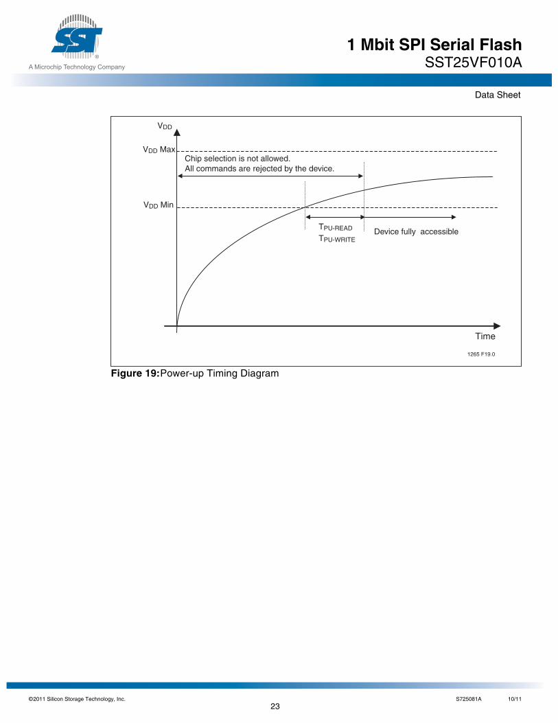
Table 10:Recommended System Power-up Timings
Symbol Parameter Minimum Units
TPU-READ1
1. This parameter is measured only for initial qualification and after a design or process change that could affect thisparameter.
VDD Min to Read Operation 10 µs
TPU-WRITE1 VDD Min to Write Operation 10 µs
T10.0 25081
Table 11:Capacitance (TA = 25°C, f=1 Mhz, other pins open)
Parameter Description Test Condition Maximum
COUT1
1. This parameter is measured only for initial qualification and after a design or process change that could affect thisparameter.
Output Pin Capacitance VOUT = 0V 12 pF
CIN1 Input Capacitance VIN = 0V 6 pF
T11.0 25081
Table 12:Reliability Characteristics
Symbol Parameter Minimum Specification Units Test Method
NEND1
1. This parameter is measured only for initial qualification and after a design or process change that could affect thisparameter.
Endurance 10,000 Cycles JEDEC Standard A117
TDR1 Data Retention 100 Years JEDEC Standard A103
ILTH1 Latch Up 100 + IDD mA JEDEC Standard 78
T12.0 25081
11 Silicon Storage Technology, Inc. S725081A 10/11
20
©20
1 Mbit SPI Serial FlashSST25VF010A
Data Sheet
A Microchip Technology Company
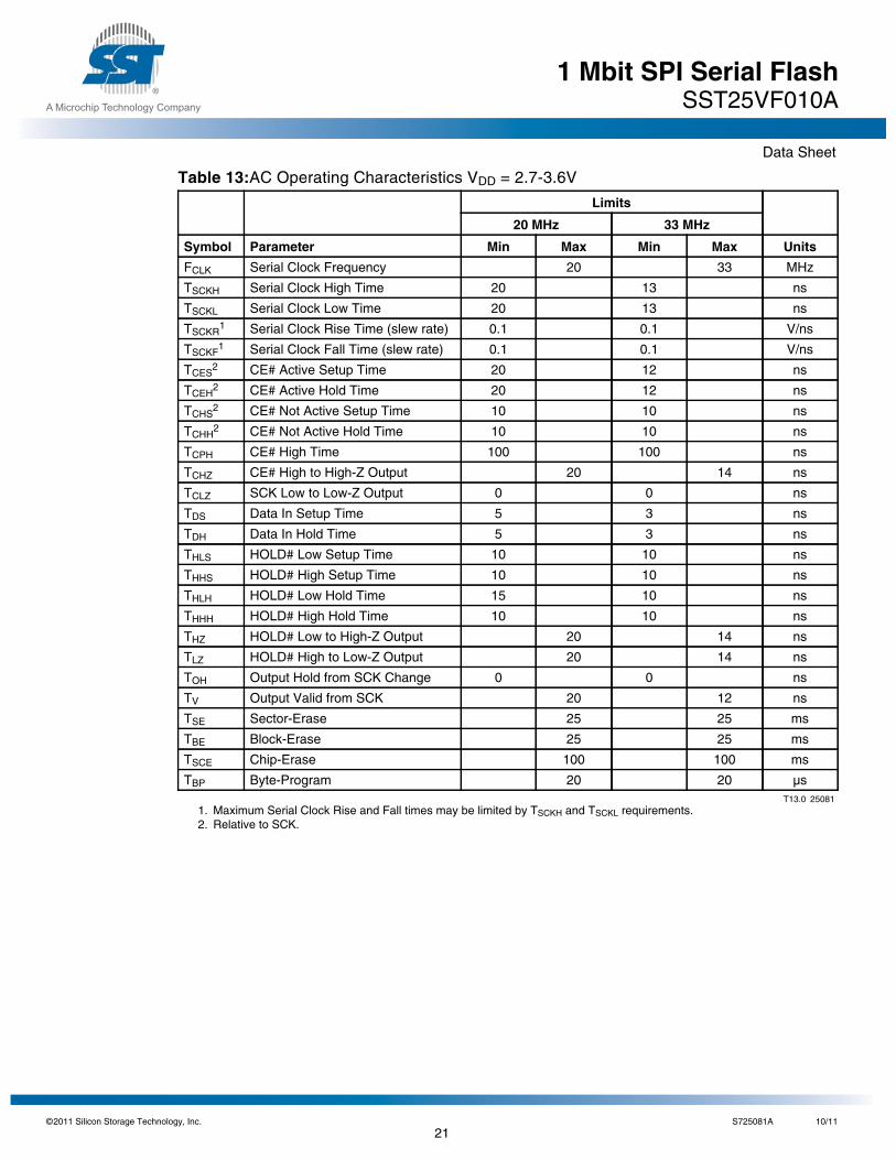
Table 13:AC Operating Characteristics VDD = 2.7-3.6V
Limits
20 MHz 33 MHz
Symbol Parameter Min Max Min Max Units
FCLK Serial Clock Frequency 20 33 MHz
TSCKH Serial Clock High Time 20 13 ns
TSCKL Serial Clock Low Time 20 13 ns
TSCKR1 Serial Clock Rise Time (slew rate) 0.1 0.1 V/ns
TSCKF1 Serial Clock Fall Time (slew rate) 0.1 0.1 V/ns
TCES2 CE# Active Setup Time 20 12 ns
TCEH2 CE# Active Hold Time 20 12 ns
TCHS2 CE# Not Active Setup Time 10 10 ns
TCHH2 CE# Not Active Hold Time 10 10 ns
TCPH CE# High Time 100 100 ns
TCHZ CE# High to High-Z Output 20 14 ns
TCLZ SCK Low to Low-Z Output 0 0 ns
TDS Data In Setup Time 5 3 ns
TDH Data In Hold Time 5 3 ns
THLS HOLD# Low Setup Time 10 10 ns
THHS HOLD# High Setup Time 10 10 ns
THLH HOLD# Low Hold Time 15 10 ns
THHH HOLD# High Hold Time 10 10 ns
THZ HOLD# Low to High-Z Output 20 14 ns
TLZ HOLD# High to Low-Z Output 20 14 ns
TOH Output Hold from SCK Change 0 0 ns
TV Output Valid from SCK 20 12 ns
TSE Sector-Erase 25 25 ms
TBE Block-Erase 25 25 ms
TSCE Chip-Erase 100 100 ms
TBP Byte-Program 20 20 µsT13.0 25081
1. Maximum Serial Clock Rise and Fall times may be limited by TSCKH and TSCKL requirements.2. Relative to SCK.
11 Silicon Storage Technology, Inc. S725081A 10/11
21
©20
1 Mbit SPI Serial FlashSST25VF010A
Data Sheet
A Microchip Technology Company
Figure 16:Serial Input Timing Diagram
Figure 17:Serial Output Timing Diagram
Figure 18:Hold Timing Diagram
HIGH-Z HIGH-Z
CE#
SO
SI
SCK
MSB LSB
TDS TDH
TCHH
TCES
TCEH TCHS
TSCKR
TSCKF
TCPH
1265 F16.0
1265 F17.0
CE#
SI
SO
SCK
MSB
TCLZ
TV
TSCKH
TCHZTOH
TSCKL
LSB
THZ TLZ
THHH THLS
THLH
THHS
1265 F18.0HOLD#
CE#
SCK
SO
SI
11 Silicon Storage Technology, Inc. S725081A 10/11
22
©20
1 Mbit SPI Serial FlashSST25VF010A
Data Sheet
A Microchip Technology Company
Figure 19:Power-up Timing Diagram
Time
VDD Min
VDD Max
VDD
Device fully accessibleTPU-READ
TPU-WRITE
Chip selection is not allowed.All commands are rejected by the device.
1265 F19.0
11 Silicon Storage Technology, Inc. S725081A 10/11
23
©20
1 Mbit SPI Serial FlashSST25VF010A
Data Sheet
A Microchip Technology Company
Figure 20:AC Input/Output Reference Waveforms
Figure 21:A Test Load Example
1265 F20.0
REFERENCE POINTS OUTPUTINPUT
VHT
VLT
VHT
VLT
VIHT
VILT
AC test inputs are driven at VIHT (0.9VDD) for a logic “1” and VILT (0.1VDD) for a logic “0”. Mea-surement reference points for inputs and outputs are VHT (0.7VDD) and VLT (0.3VDD). Inputrise and fall times (10% 90%) are <5 ns.
Note: VHT - VHIGH TestVLT - VLOW TestVIHT - VINPUT HIGH TestVILT - VINPUT LOW Test
1265 F21.0
TO TESTER
TO DUT
CL
11 Silicon Storage Technology, Inc. S725081A 10/11
24
©20
1 Mbit SPI Serial FlashSST25VF010A
Data Sheet
A Microchip Technology Company
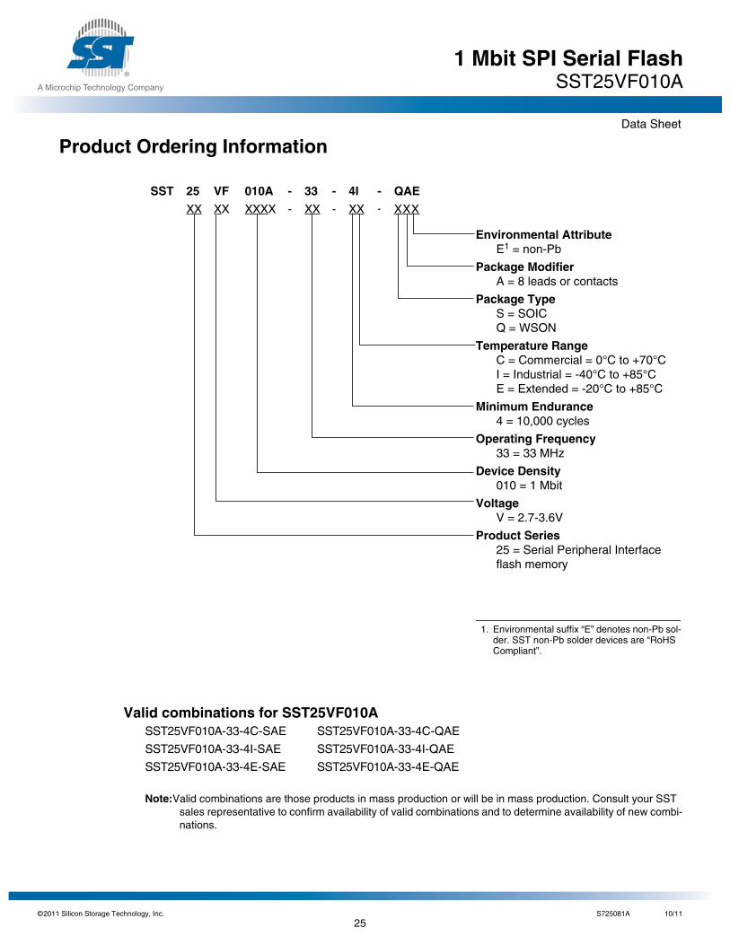
Product Ordering Information
Valid combinations for SST25VF010ASST25VF010A-33-4C-SAE SST25VF010A-33-4C-QAE
SST25VF010A-33-4I-SAE SST25VF010A-33-4I-QAE
SST25VF010A-33-4E-SAE SST25VF010A-33-4E-QAE
Note:Valid combinations are those products in mass production or will be in mass production. Consult your SSTsales representative to confirm availability of valid combinations and to determine availability of new combi-nations.
SST 25 VF 010A - 33 - 4I - QAE
XX XX XXXX - XX - XX - XXX
Environmental AttributeE1 = non-Pb
Package ModifierA = 8 leads or contacts
Package TypeS = SOICQ = WSON
Temperature RangeC = Commercial = 0°C to +70°CI = Industrial = -40°C to +85°CE = Extended = -20°C to +85°C
Minimum Endurance4 = 10,000 cycles
Operating Frequency33 = 33 MHz
Device Density010 = 1 Mbit
VoltageV = 2.7-3.6V
Product Series25 = Serial Peripheral Interfaceflash memory
1. Environmental suffix “E” denotes non-Pb sol-der. SST non-Pb solder devices are “RoHSCompliant”.
11 Silicon Storage Technology, Inc. S725081A 10/11
25
©20
1 Mbit SPI Serial FlashSST25VF010A
Data Sheet
A Microchip Technology Company
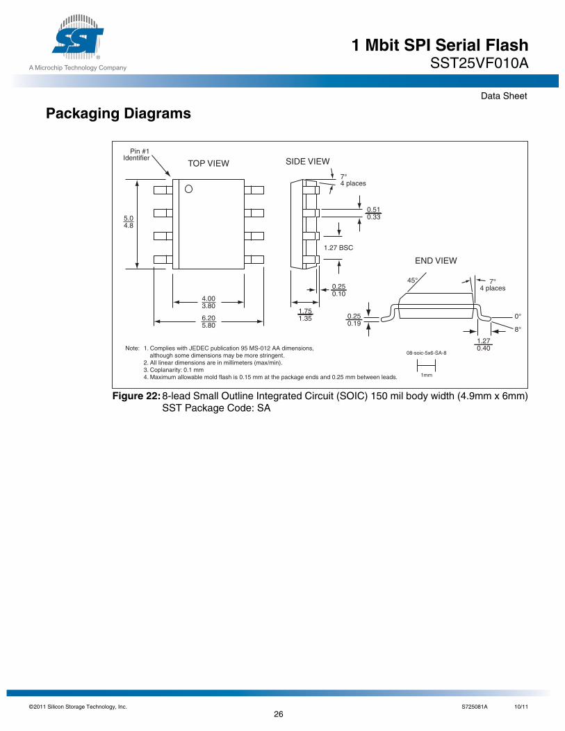
Packaging Diagrams
Figure 22:8-lead Small Outline Integrated Circuit (SOIC) 150 mil body width (4.9mm x 6mm)SST Package Code: SA
08-soic-5x6-SA-8Note: 1. Complies with JEDEC publication 95 MS-012 AA dimensions,
although some dimensions may be more stringent.2. All linear dimensions are in millimeters (max/min).3. Coplanarity: 0.1 mm4. Maximum allowable mold flash is 0.15 mm at the package ends and 0.25 mm between leads.
TOP VIEW SIDE VIEW
END VIEW
5.04.8
6.205.80
4.003.80
Pin #1Identifier
0.510.33
1.27 BSC
0.250.10
1.751.35
7°4 places
0.250.19
1.270.40
45° 7°4 places
0°
8°
1mm
11 Silicon Storage Technology, Inc. S725081A 10/11
26
©20
1 Mbit SPI Serial FlashSST25VF010A
Data Sheet
A Microchip Technology Company
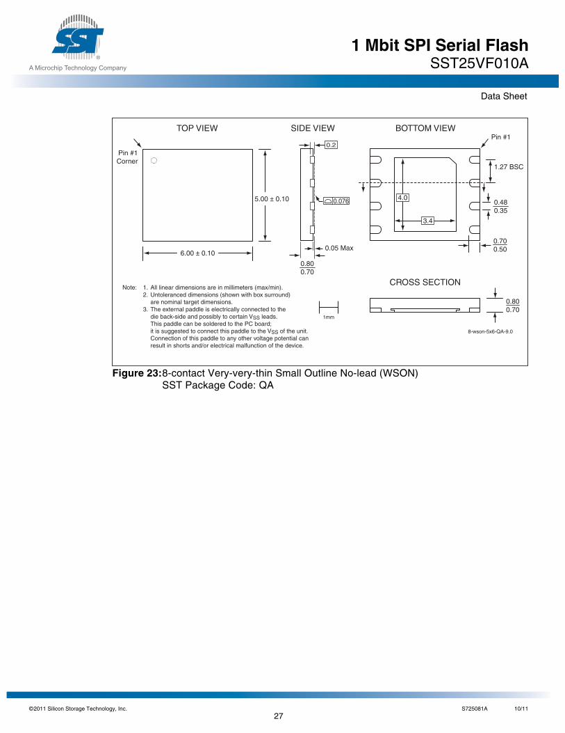
Figure 23:8-contact Very-very-thin Small Outline No-lead (WSON)SST Package Code: QA
Note: 1. All linear dimensions are in millimeters (max/min).2. Untoleranced dimensions (shown with box surround)
are nominal target dimensions.3. The external paddle is electrically connected to the
die back-side and possibly to certain VSS leads.This paddle can be soldered to the PC board;it is suggested to connect this paddle to the VSS of the unit.Connection of this paddle to any other voltage potential canresult in shorts and/or electrical malfunction of the device.
8-wson-5x6-QA-9.0
4.0
1.27 BSC
Pin #1
0.480.35
0.076
3.4
5.00 ± 0.10
6.00 ± 0.100.05 Max
0.700.50
0.800.70
0.800.70
Pin #1Corner
TOP VIEW BOTTOM VIEW
CROSS SECTION
SIDE VIEW
1mm
0.2
11 Silicon Storage Technology, Inc. S725081A 10/11
27
©20
1 Mbit SPI Serial FlashSST25VF010A
Data Sheet
A Microchip Technology Company
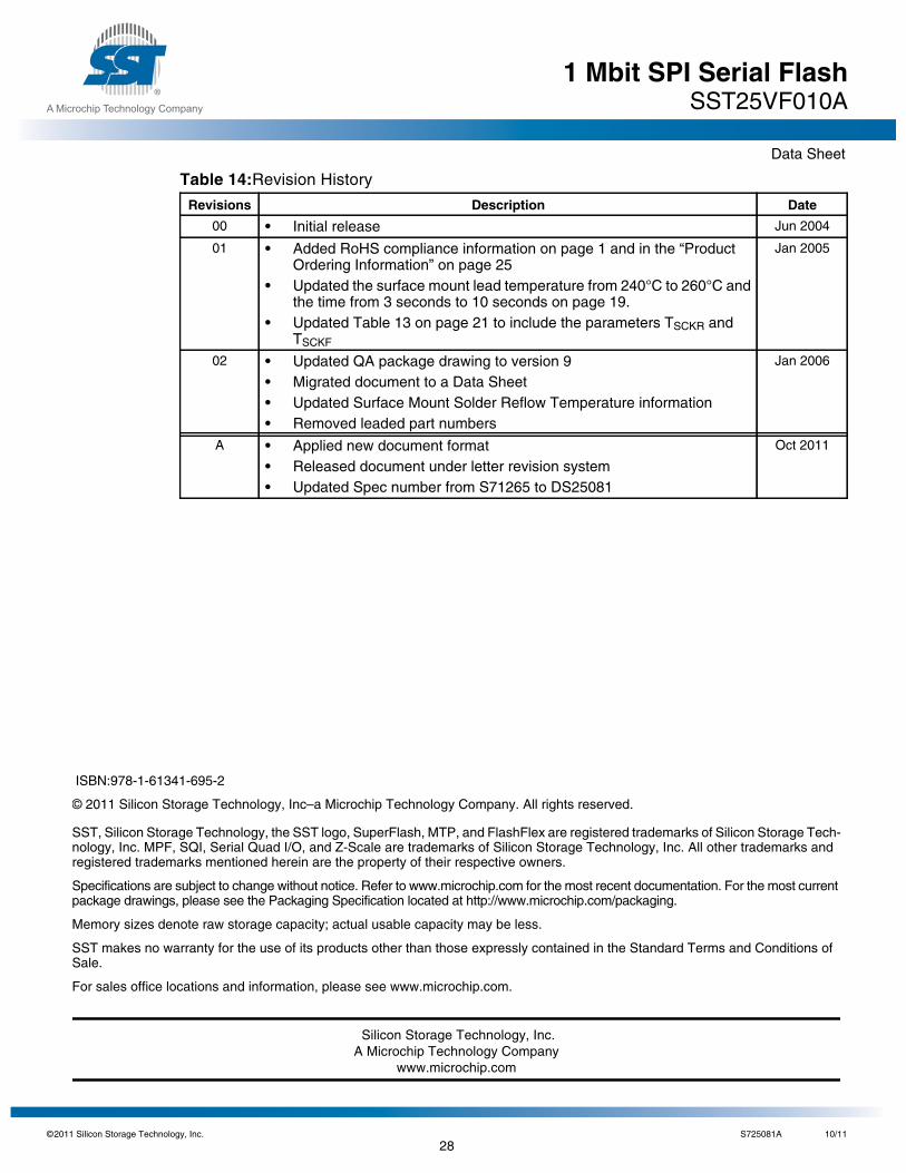
Table 14:Revision History
Revisions Description Date
00 • Initial release Jun 2004
01 • Added RoHS compliance information on page 1 and in the “ProductOrdering Information” on page 25
• Updated the surface mount lead temperature from 240°C to 260°C andthe time from 3 seconds to 10 seconds on page 19.
• Updated Table 13 on page 21 to include the parameters TSCKR andTSCKF
Jan 2005
02 • Updated QA package drawing to version 9• Migrated document to a Data Sheet• Updated Surface Mount Solder Reflow Temperature information• Removed leaded part numbers
Jan 2006
A • Applied new document format• Released document under letter revision system• Updated Spec number from S71265 to DS25081
Oct 2011
© 2011 Silicon Storage Technology, Inc–a Microchip Technology Company. All rights reserved.
SST, Silicon Storage Technology, the SST logo, SuperFlash, MTP, and FlashFlex are registered trademarks of Silicon Storage Tech-nology, Inc. MPF, SQI, Serial Quad I/O, and Z-Scale are trademarks of Silicon Storage Technology, Inc. All other trademarks andregistered trademarks mentioned herein are the property of their respective owners.
Specifications are subject to change without notice. Refer to www.microchip.com for the most recent documentation. For the most currentpackage drawings, please see the Packaging Specification located at http://www.microchip.com/packaging.
Memory sizes denote raw storage capacity; actual usable capacity may be less.
SST makes no warranty for the use of its products other than those expressly contained in the Standard Terms and Conditions ofSale.
For sales office locations and information, please see www.microchip.com.
Silicon Storage Technology, Inc.A Microchip Technology Company
www.microchip.com
ISBN:978-1-61341-695-2
11 Silicon Storage Technology, Inc. S725081A 10/11
28