Embed Size (px)
Citation preview

This is information on a product in full production.
November 2017 DocID13264 Rev 15 1/53
M95M01-DF M95M01-R
1-Mbit serial SPI bus EEPROM
Datasheet - production data
Features
• Compatible with the Serial Peripheral Interface (SPI) bus
• Memory array
– 1 Mbit (128 Kbytes) of EEPROM
– Page size: 256 bytes
• Write
– Byte Write within 5 ms
– Page Write within 5 ms
• Additional Write lockable page (Identification Page)
• Write Protect: quarter, half or whole memory array
• High-speed clock: 16 MHz
• Single supply voltage:
– 1.8 V to 5.5 V for M95M01-R
– 1.7 V to 5.5 V for M95M01-DF
• Operating temperature range: from -40 °C up to +85 °C
• Enhanced ESD protection
• More than 4 million Write cycles
• More than 200-year data retention
• Packages:
– SO8 (ECOPACK2®)
– TSSOP8 (ECOPACK2®)
– WLCSP (ECOPACK2®)
– Unsawn wafer (each die is tested)
SO8 (MN)150 mil width
TSSOP8 (DW)169 mil width
WLCSP (CS and CU)
Unsawn wafer
www.st.com

Contents M95M01-DF M95M01-R
2/53 DocID13264 Rev 15
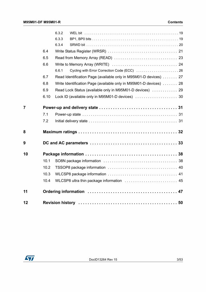
Contents
1 Description . . . . . . . . . . . . . . . . . . . . . . . . . . . . . . . . . . . . . . . . . . . . . . . . . 6
2 Memory organization . . . . . . . . . . . . . . . . . . . . . . . . . . . . . . . . . . . . . . . . 8
3 Signal description . . . . . . . . . . . . . . . . . . . . . . . . . . . . . . . . . . . . . . . . . . . 9
3.1 Serial Data Output (Q) . . . . . . . . . . . . . . . . . . . . . . . . . . . . . . . . . . . . . . . . 9
3.2 Serial Data Input (D) . . . . . . . . . . . . . . . . . . . . . . . . . . . . . . . . . . . . . . . . . . 9
3.3 Serial Clock (C) . . . . . . . . . . . . . . . . . . . . . . . . . . . . . . . . . . . . . . . . . . . . . 9
3.4 Chip Select (S) . . . . . . . . . . . . . . . . . . . . . . . . . . . . . . . . . . . . . . . . . . . . . . 9
3.5 Hold (HOLD) . . . . . . . . . . . . . . . . . . . . . . . . . . . . . . . . . . . . . . . . . . . . . . . . 9
3.6 Write Protect (W) . . . . . . . . . . . . . . . . . . . . . . . . . . . . . . . . . . . . . . . . . . . 10
3.7 VCC supply voltage . . . . . . . . . . . . . . . . . . . . . . . . . . . . . . . . . . . . . . . . . . 10
3.8 VSS ground . . . . . . . . . . . . . . . . . . . . . . . . . . . . . . . . . . . . . . . . . . . . . . . . 10
4 Connecting to the SPI bus . . . . . . . . . . . . . . . . . . . . . . . . . . . . . . . . . . . 11
4.1 SPI modes . . . . . . . . . . . . . . . . . . . . . . . . . . . . . . . . . . . . . . . . . . . . . . . . 12
5 Operating features . . . . . . . . . . . . . . . . . . . . . . . . . . . . . . . . . . . . . . . . . 13
5.1 Supply voltage (VCC) . . . . . . . . . . . . . . . . . . . . . . . . . . . . . . . . . . . . . . . . 13
5.1.1 Operating supply voltage (VCC) . . . . . . . . . . . . . . . . . . . . . . . . . . . . . . . 13
5.1.2 Device reset . . . . . . . . . . . . . . . . . . . . . . . . . . . . . . . . . . . . . . . . . . . . . . 13
5.1.3 Power-up conditions . . . . . . . . . . . . . . . . . . . . . . . . . . . . . . . . . . . . . . . 13
5.1.4 Power-down . . . . . . . . . . . . . . . . . . . . . . . . . . . . . . . . . . . . . . . . . . . . . . 14
5.2 Active Power and Standby Power modes . . . . . . . . . . . . . . . . . . . . . . . . 14
5.3 Hold condition . . . . . . . . . . . . . . . . . . . . . . . . . . . . . . . . . . . . . . . . . . . . . . 14
5.4 Status Register . . . . . . . . . . . . . . . . . . . . . . . . . . . . . . . . . . . . . . . . . . . . . 15
5.5 Data protection and protocol control . . . . . . . . . . . . . . . . . . . . . . . . . . . . 15
6 Instructions . . . . . . . . . . . . . . . . . . . . . . . . . . . . . . . . . . . . . . . . . . . . . . . 16
6.1 Write Enable (WREN) . . . . . . . . . . . . . . . . . . . . . . . . . . . . . . . . . . . . . . . 17
6.2 Write Disable (WRDI) . . . . . . . . . . . . . . . . . . . . . . . . . . . . . . . . . . . . . . . . 18
6.3 Read Status Register (RDSR) . . . . . . . . . . . . . . . . . . . . . . . . . . . . . . . . . 19
6.3.1 WIP bit . . . . . . . . . . . . . . . . . . . . . . . . . . . . . . . . . . . . . . . . . . . . . . . . . . 19
DocID13264 Rev 15 3/53
M95M01-DF M95M01-R Contents
3
6.3.2 WEL bit . . . . . . . . . . . . . . . . . . . . . . . . . . . . . . . . . . . . . . . . . . . . . . . . . 19
6.3.3 BP1, BP0 bits . . . . . . . . . . . . . . . . . . . . . . . . . . . . . . . . . . . . . . . . . . . . . 19
6.3.4 SRWD bit . . . . . . . . . . . . . . . . . . . . . . . . . . . . . . . . . . . . . . . . . . . . . . . . 20
6.4 Write Status Register (WRSR) . . . . . . . . . . . . . . . . . . . . . . . . . . . . . . . . . 21
6.5 Read from Memory Array (READ) . . . . . . . . . . . . . . . . . . . . . . . . . . . . . . 23
6.6 Write to Memory Array (WRITE) . . . . . . . . . . . . . . . . . . . . . . . . . . . . . . . 24
6.6.1 Cycling with Error Correction Code (ECC) . . . . . . . . . . . . . . . . . . . . . . 26
6.7 Read Identification Page (available only in M95M01-D devices) . . . . . . . 27
6.8 Write Identification Page (available only in M95M01-D devices) . . . . . . . 28
6.9 Read Lock Status (available only in M95M01-D devices) . . . . . . . . . . . . 29
6.10 Lock ID (available only in M95M01-D devices) . . . . . . . . . . . . . . . . . . . . 30
7 Power-up and delivery state . . . . . . . . . . . . . . . . . . . . . . . . . . . . . . . . . . 31
7.1 Power-up state . . . . . . . . . . . . . . . . . . . . . . . . . . . . . . . . . . . . . . . . . . . . . 31
7.2 Initial delivery state . . . . . . . . . . . . . . . . . . . . . . . . . . . . . . . . . . . . . . . . . . 31
8 Maximum ratings . . . . . . . . . . . . . . . . . . . . . . . . . . . . . . . . . . . . . . . . . . . 32
9 DC and AC parameters . . . . . . . . . . . . . . . . . . . . . . . . . . . . . . . . . . . . . . 33
10 Package information . . . . . . . . . . . . . . . . . . . . . . . . . . . . . . . . . . . . . . . . 38
10.1 SO8N package information . . . . . . . . . . . . . . . . . . . . . . . . . . . . . . . . . . . 38
10.2 TSSOP8 package information . . . . . . . . . . . . . . . . . . . . . . . . . . . . . . . . . 40
10.3 WLCSP8 package information . . . . . . . . . . . . . . . . . . . . . . . . . . . . . . . . . 41
10.4 WLCSP8 ultra thin package information . . . . . . . . . . . . . . . . . . . . . . . . . 45
11 Ordering information . . . . . . . . . . . . . . . . . . . . . . . . . . . . . . . . . . . . . . . 47
12 Revision history . . . . . . . . . . . . . . . . . . . . . . . . . . . . . . . . . . . . . . . . . . . 50
List of tables M95M01-DF M95M01-R
4/53 DocID13264 Rev 15
List of tables
Table 1. Signal names . . . . . . . . . . . . . . . . . . . . . . . . . . . . . . . . . . . . . . . . . . . . . . . . . . . . . . . . . . . . 6Table 2. Write-protected block size . . . . . . . . . . . . . . . . . . . . . . . . . . . . . . . . . . . . . . . . . . . . . . . . . 15Table 3. Instruction set . . . . . . . . . . . . . . . . . . . . . . . . . . . . . . . . . . . . . . . . . . . . . . . . . . . . . . . . . . . 16Table 4. Status Register format . . . . . . . . . . . . . . . . . . . . . . . . . . . . . . . . . . . . . . . . . . . . . . . . . . . . 20Table 5. Protection modes . . . . . . . . . . . . . . . . . . . . . . . . . . . . . . . . . . . . . . . . . . . . . . . . . . . . . . . . 22Table 6. Address range bits . . . . . . . . . . . . . . . . . . . . . . . . . . . . . . . . . . . . . . . . . . . . . . . . . . . . . . . 23Table 7. Absolute maximum ratings . . . . . . . . . . . . . . . . . . . . . . . . . . . . . . . . . . . . . . . . . . . . . . . . . 32Table 8. Operating conditions (M95M01-R, device grade 6) . . . . . . . . . . . . . . . . . . . . . . . . . . . . . . 33Table 9. Operating conditions (M95M01-DF, device grade 6) . . . . . . . . . . . . . . . . . . . . . . . . . . . . . 33Table 10. AC measurement conditions. . . . . . . . . . . . . . . . . . . . . . . . . . . . . . . . . . . . . . . . . . . . . . . . 33Table 11. Cycling performance by groups of four bytes . . . . . . . . . . . . . . . . . . . . . . . . . . . . . . . . . . . 34Table 12. Memory cell data retention . . . . . . . . . . . . . . . . . . . . . . . . . . . . . . . . . . . . . . . . . . . . . . . . . 34Table 13. Capacitance . . . . . . . . . . . . . . . . . . . . . . . . . . . . . . . . . . . . . . . . . . . . . . . . . . . . . . . . . . . . 34Table 14. DC characteristics. . . . . . . . . . . . . . . . . . . . . . . . . . . . . . . . . . . . . . . . . . . . . . . . . . . . . . . . 35Table 15. AC characteristics. . . . . . . . . . . . . . . . . . . . . . . . . . . . . . . . . . . . . . . . . . . . . . . . . . . . . . . . 36Table 16. SO8N – 8-lead plastic small outline, 150 mils body width,
package mechanical data . . . . . . . . . . . . . . . . . . . . . . . . . . . . . . . . . . . . . . . . . . . . . . . . . . 38Table 17. TSSOP8 – 8-lead thin shrink small outline, 3 x 4.4 mm, 0.65 mm pitch,
package mechanical data . . . . . . . . . . . . . . . . . . . . . . . . . . . . . . . . . . . . . . . . . . . . . . . . . . 40Table 18. WLCSP- 8-bump, without BSC, 2.578 x 1.716 mm, wafer level chip scale
package mechanical data . . . . . . . . . . . . . . . . . . . . . . . . . . . . . . . . . . . . . . . . . . . . . . . . . . 41Table 19. WLCSP- 8-bump, with BSC, 2.578 x 1.716 mm, wafer level chip scale
package mechanical data . . . . . . . . . . . . . . . . . . . . . . . . . . . . . . . . . . . . . . . . . . . . . . . . . . 43Table 20. WLCSP - 8 balls, 2.578x1.716 mm, 0.5 mm pitch, with BSC,
wafer level chip scale mechanical data . . . . . . . . . . . . . . . . . . . . . . . . . . . . . . . . . . . . . . . 45Table 21. Ordering information scheme . . . . . . . . . . . . . . . . . . . . . . . . . . . . . . . . . . . . . . . . . . . . . . . 47Table 22. Ordering information scheme (unsawn wafer) . . . . . . . . . . . . . . . . . . . . . . . . . . . . . . . . . . 48Table 23. Document revision history . . . . . . . . . . . . . . . . . . . . . . . . . . . . . . . . . . . . . . . . . . . . . . . . . 50
DocID13264 Rev 15 5/53
M95M01-DF M95M01-R List of figures
5
List of figures
Figure 1. Logic diagram . . . . . . . . . . . . . . . . . . . . . . . . . . . . . . . . . . . . . . . . . . . . . . . . . . . . . . . . . . . . 6Figure 2. 8-pin package connections (top view) . . . . . . . . . . . . . . . . . . . . . . . . . . . . . . . . . . . . . . . . . 7Figure 3. WLCSP connections for M95M01-DFCS6TP/K and M95M01-DFCU6TP/K
(top view, marking side, with bumps on the underside) . . . . . . . . . . . . . . . . . . . . . . . . . . . . 7Figure 4. Block diagram . . . . . . . . . . . . . . . . . . . . . . . . . . . . . . . . . . . . . . . . . . . . . . . . . . . . . . . . . . . . 8Figure 5. Bus master and memory devices on the SPI bus. . . . . . . . . . . . . . . . . . . . . . . . . . . . . . . . 11Figure 6. SPI modes supported . . . . . . . . . . . . . . . . . . . . . . . . . . . . . . . . . . . . . . . . . . . . . . . . . . . . . 12Figure 7. Hold condition activation. . . . . . . . . . . . . . . . . . . . . . . . . . . . . . . . . . . . . . . . . . . . . . . . . . . 14Figure 8. Write Enable (WREN) sequence . . . . . . . . . . . . . . . . . . . . . . . . . . . . . . . . . . . . . . . . . . . . 17Figure 9. Write Disable (WRDI) sequence. . . . . . . . . . . . . . . . . . . . . . . . . . . . . . . . . . . . . . . . . . . . . 18Figure 10. Read Status Register (RDSR) sequence . . . . . . . . . . . . . . . . . . . . . . . . . . . . . . . . . . . . . . 19Figure 11. Write Status Register (WRSR) sequence. . . . . . . . . . . . . . . . . . . . . . . . . . . . . . . . . . . . . . 21Figure 12. Read from Memory Array (READ) sequence . . . . . . . . . . . . . . . . . . . . . . . . . . . . . . . . . . . 23Figure 13. Byte Write (WRITE) sequence . . . . . . . . . . . . . . . . . . . . . . . . . . . . . . . . . . . . . . . . . . . . . . 24Figure 14. Page Write (WRITE) sequence . . . . . . . . . . . . . . . . . . . . . . . . . . . . . . . . . . . . . . . . . . . . . 25Figure 15. Read Identification Page sequence . . . . . . . . . . . . . . . . . . . . . . . . . . . . . . . . . . . . . . . . . . 27Figure 16. Write Identification Page sequence . . . . . . . . . . . . . . . . . . . . . . . . . . . . . . . . . . . . . . . . . . 28Figure 17. Read Lock Status sequence . . . . . . . . . . . . . . . . . . . . . . . . . . . . . . . . . . . . . . . . . . . . . . . 29Figure 18. Lock ID sequence . . . . . . . . . . . . . . . . . . . . . . . . . . . . . . . . . . . . . . . . . . . . . . . . . . . . . . . 30Figure 19. AC measurement I/O waveform . . . . . . . . . . . . . . . . . . . . . . . . . . . . . . . . . . . . . . . . . . . . . 33Figure 20. Serial input timing . . . . . . . . . . . . . . . . . . . . . . . . . . . . . . . . . . . . . . . . . . . . . . . . . . . . . . . . 37Figure 21. Hold timing . . . . . . . . . . . . . . . . . . . . . . . . . . . . . . . . . . . . . . . . . . . . . . . . . . . . . . . . . . . . . 37Figure 22. Serial output timing . . . . . . . . . . . . . . . . . . . . . . . . . . . . . . . . . . . . . . . . . . . . . . . . . . . . . . . 37Figure 23. SO8N – 8-lead plastic small outline, 150 mils body width, package outline . . . . . . . . . . . . 38Figure 24. SO8N – 8-lead plastic small outline, 150 mils body width,
package recommended footprint . . . . . . . . . . . . . . . . . . . . . . . . . . . . . . . . . . . . . . . . . . . . 39Figure 25. TSSOP8 – 8-lead thin shrink small outline, 3 x 4.4 mm, 0.65 mm pitch,
package outline. . . . . . . . . . . . . . . . . . . . . . . . . . . . . . . . . . . . . . . . . . . . . . . . . . . . . . . . . . 40Figure 26. WLCSP- 8-bump, without BSC, 2.578 x 1.716 mm, wafer level chip scale
package outline. . . . . . . . . . . . . . . . . . . . . . . . . . . . . . . . . . . . . . . . . . . . . . . . . . . . . . . . . . 41Figure 27. WLCSP- 8-bump, with BSC, 2.578 x 1716 mm, wafer level chip scale
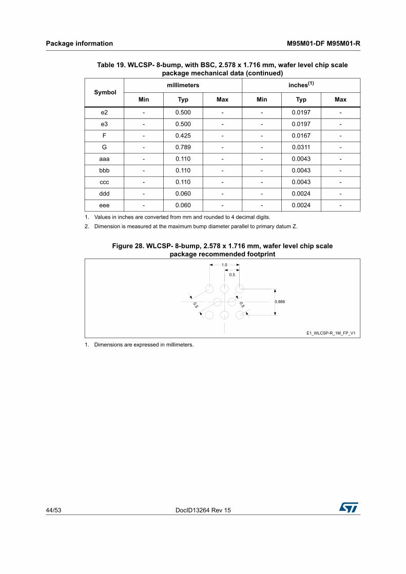
package outline. . . . . . . . . . . . . . . . . . . . . . . . . . . . . . . . . . . . . . . . . . . . . . . . . . . . . . . . . . 43Figure 28. WLCSP- 8-bump, 2.578 x 1.716 mm, wafer level chip scale
package recommended footprint . . . . . . . . . . . . . . . . . . . . . . . . . . . . . . . . . . . . . . . . . . . . 44Figure 29. WLCSP - 8 balls, 2.578x1.716 mm, 0.5 mm pitch, with BSC,
wafer level chip scale package outline . . . . . . . . . . . . . . . . . . . . . . . . . . . . . . . . . . . . . . . . 45Figure 30. WLCSP - 8 balls, 2.578x1.716 mm, 0.5 mm pitch, with BSC,
wafer level chip scale recommended footprint . . . . . . . . . . . . . . . . . . . . . . . . . . . . . . . . . . 46
Description M95M01-DF M95M01-R
6/53 DocID13264 Rev 15
1 Description
The M95M01 devices are Electrically Erasable PROgrammable Memories (EEPROMs) organized as 131072 x 8 bits, accessed through the SPI bus.
The M95M01-R can operate with a supply range from 1.8 V to 5.5 V, the M95M01-DF can operate with a supply range from 1.7 V up to 5.5 V. These devices are guaranteed over the -40 °C/+85 °C temperature range.
The M95M01-DF offers an additional page, named the Identification Page (256 bytes). The Identification Page can be used to store sensitive application parameters that can be (later) permanently locked in Read-only mode.
Figure 1. Logic diagram
The SPI bus signals are C, D and Q, as shown in Figure 1 and Table 1. The device is selected when Chip Select (S) is driven low. Communications with the device can be interrupted when the HOLD is driven low.
Table 1. Signal names
Signal name Function Direction
C Serial Clock Input
D Serial Data Input Input
Q Serial Data Output Output
S Chip Select Input
W Write Protect Input
HOLD Hold Input
VCC Supply voltage -
VSS Ground -
DocID13264 Rev 15 7/53
M95M01-DF M95M01-R Description
37
Figure 2. 8-pin package connections (top view)
1. See Section 10: Package information for package dimensions, and how to identify pin-1.
Figure 3. WLCSP connections for M95M01-DFCS6TP/K and M95M01-DFCU6TP/K(top view, marking side, with bumps on the underside)
Memory organization M95M01-DF M95M01-R
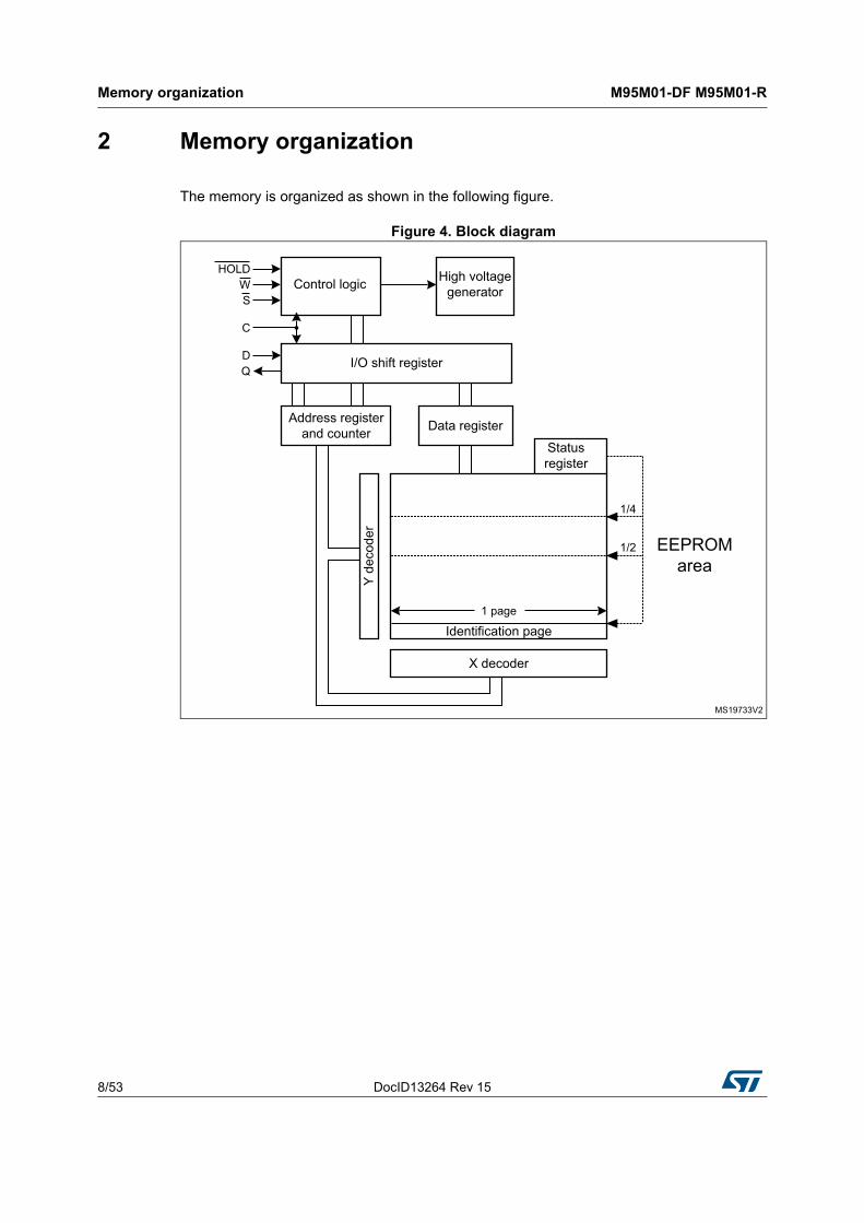
8/53 DocID13264 Rev 15
2 Memory organization
The memory is organized as shown in the following figure.
Figure 4. Block diagram

DocID13264 Rev 15 9/53
M95M01-DF M95M01-R Signal description
37
3 Signal description
During all operations, VCC must be held stable and within the specified valid range: VCC(min) to VCC(max).
All of the input and output signals must be held high or low (according to voltages of VIH, VOH, VIL or VOL, as specified in Section 9: DC and AC parameters). These signals are described next.
3.1 Serial Data Output (Q)
This output signal is used to transfer data serially out of the device. Data is shifted out on the falling edge of Serial Clock (C).
3.2 Serial Data Input (D)
This input signal is used to transfer data serially into the device. It receives instructions, addresses, and the data to be written. Values are latched on the rising edge of Serial Clock (C).
3.3 Serial Clock (C)
This input signal provides the timing of the serial interface. Instructions, addresses, or data present at Serial Data Input (D) are latched on the rising edge of Serial Clock (C). Data on Serial Data Output (Q) change from the falling edge of Serial Clock (C).
3.4 Chip Select (S)
When this input signal is high, the device is deselected and Serial Data Output (Q) is at high impedance. The device is in the Standby Power mode, unless an internal Write cycle is in progress. Driving Chip Select (S) low selects the device, placing it in the Active Power mode.
After power-up, a falling edge on Chip Select (S) is required prior to the start of any instruction.
3.5 Hold (HOLD)
The Hold (HOLD) signal is used to pause any serial communications with the device without deselecting the device.
During the Hold condition, the Serial Data Output (Q) is high impedance, and Serial Data Input (D) and Serial Clock (C) are Don’t Care.
To start the Hold condition, the device must be selected, with Chip Select (S) driven low.

Signal description M95M01-DF M95M01-R
10/53 DocID13264 Rev 15
3.6 Write Protect (W)
The main purpose of this input signal is to freeze the size of the area of memory that is protected against Write instructions (as specified by the values in the BP1 and BP0 bits of the Status Register).
This pin must be driven either high or low, and must be stable during all Write instructions.
3.7 VCC supply voltage
VCC is the supply voltage.
3.8 VSS ground
VSS is the reference for all signals, including the VCC supply voltage.
DocID13264 Rev 15 11/53
M95M01-DF M95M01-R Connecting to the SPI bus
37
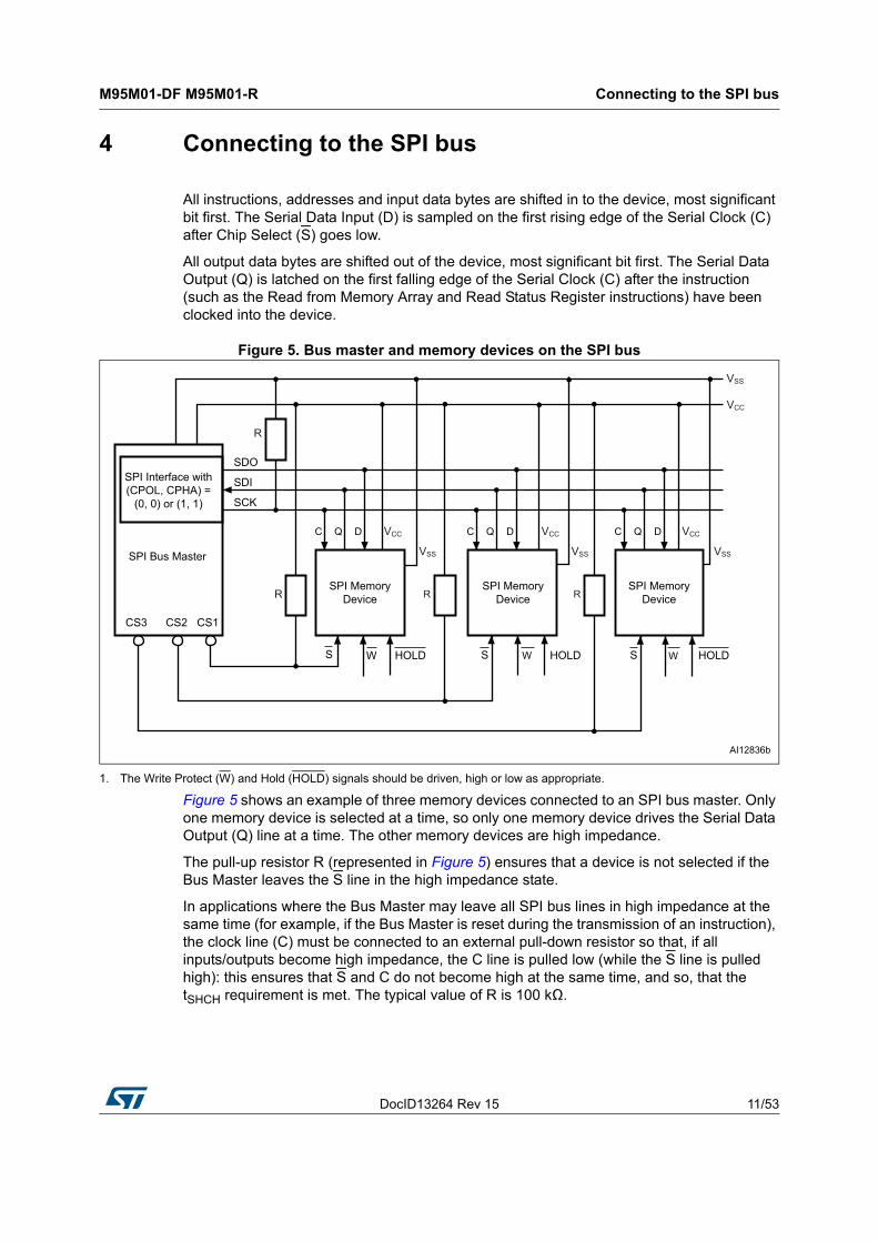
4 Connecting to the SPI bus
All instructions, addresses and input data bytes are shifted in to the device, most significant bit first. The Serial Data Input (D) is sampled on the first rising edge of the Serial Clock (C) after Chip Select (S) goes low.
All output data bytes are shifted out of the device, most significant bit first. The Serial Data Output (Q) is latched on the first falling edge of the Serial Clock (C) after the instruction (such as the Read from Memory Array and Read Status Register instructions) have been clocked into the device.
Figure 5. Bus master and memory devices on the SPI bus
1. The Write Protect (W) and Hold (HOLD) signals should be driven, high or low as appropriate.
Figure 5 shows an example of three memory devices connected to an SPI bus master. Only one memory device is selected at a time, so only one memory device drives the Serial Data Output (Q) line at a time. The other memory devices are high impedance.
The pull-up resistor R (represented in Figure 5) ensures that a device is not selected if the Bus Master leaves the S line in the high impedance state.
In applications where the Bus Master may leave all SPI bus lines in high impedance at the same time (for example, if the Bus Master is reset during the transmission of an instruction), the clock line (C) must be connected to an external pull-down resistor so that, if all inputs/outputs become high impedance, the C line is pulled low (while the S line is pulled high): this ensures that S and C do not become high at the same time, and so, that the tSHCH requirement is met. The typical value of R is 100 kΩ.

Connecting to the SPI bus M95M01-DF M95M01-R
12/53 DocID13264 Rev 15
4.1 SPI modes
These devices can be driven by a microcontroller with its SPI peripheral running in either of the following two modes:
• CPOL = 0, CPHA = 0
• CPOL = 1, CPHA = 1
For these two modes, input data is latched in on the rising edge of Serial Clock (C), and output data is available from the falling edge of Serial Clock (C).
The difference between the two modes, as shown in Figure 6, is the clock polarity when the bus master is in Stand-by mode and not transferring data:
• C remains at 0 for (CPOL = 0, CPHA = 0)
• C remains at 1 for (CPOL = 1, CPHA = 1)
Figure 6. SPI modes supported
DocID13264 Rev 15 13/53
M95M01-DF M95M01-R Operating features
37
5 Operating features
5.1 Supply voltage (VCC)
5.1.1 Operating supply voltage (VCC)
Prior to selecting the memory and issuing instructions to it, a valid and stable VCC voltage within the specified [VCC(min), VCC(max)] range must be applied (see Operating conditions in Section 9: DC and AC parameters). This voltage must remain stable and valid until the end of the transmission of the instruction and, for a Write instruction, until the completion of the internal write cycle (tW). In order to secure a stable DC supply voltage, it is recommended to decouple the VCC line with a suitable capacitor (usually of the order of 10 nF to 100 nF) close to the VCC / VSS device pins.
5.1.2 Device reset
In order to prevent erroneous instruction decoding and inadvertent Write operations during power-up, a power-on-reset (POR) circuit is included. At power-up, the device does not respond to any instruction until VCC reaches the POR threshold voltage. This threshold is lower than the minimum VCC operating voltage (see Operating conditions in Section 9).
At power-up, when VCC passes over the POR threshold, the device is reset and is in the following state:
• in Standby Power mode,
• deselected,
• Status Register values:
– The Write Enable Latch (WEL) bit is reset to 0.
– The Write In Progress (WIP) bit is reset to 0.
– The SRWD, BP1 and BP0 bits remain unchanged (non-volatile bits).
It is important to note that the device must not be accessed until VCC reaches a valid and stable level within the specified [VCC(min), VCC(max)] range, as defined under Operating conditions in Section 9.
5.1.3 Power-up conditions
When the power supply is turned on, VCC rises continuously from VSS to VCC. During this time, the Chip Select (S) line is not allowed to float but should follow the VCC voltage. It is therefore recommended to connect the S line to VCC via a suitable pull-up resistor (see Figure 5).
In addition, the Chip Select (S) input offers a built-in safety feature, as the S input is edge-sensitive as well as level-sensitive: after power-up, the device does not become selected until a falling edge has first been detected on Chip Select (S). This ensures that Chip Select (S) must have been high, prior to going low to start the first operation.
The VCC voltage has to rise continuously from 0 V up to the minimum VCC operating voltage defined under Operating conditions in Section 9.
Operating features M95M01-DF M95M01-R
14/53 DocID13264 Rev 15
5.1.4 Power-down
During power-down (continuous decrease of the VCC supply voltage below the minimum VCC operating voltage defined under Operating conditions in Section 9), the device must be:
• deselected (Chip Select S should be allowed to follow the voltage applied on VCC),
• in Standby Power mode (there should not be any internal write cycle in progress).
5.2 Active Power and Standby Power modes
When Chip Select (S) is low, the device is selected, and in the Active Power mode. The device consumes ICC.
When Chip Select (S) is high, the device is deselected. If a Write cycle is not currently in progress, the device then goes into the Standby Power mode, and the device consumption drops to ICC1, as specified in DC characteristics (see Section 9).
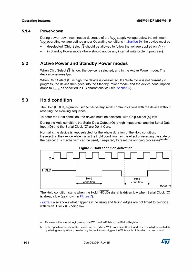
5.3 Hold condition
The Hold (HOLD) signal is used to pause any serial communications with the device without resetting the clocking sequence.
To enter the Hold condition, the device must be selected, with Chip Select (S) low.
During the Hold condition, the Serial Data Output (Q) is high impedance, and the Serial Data Input (D) and the Serial Clock (C) are Don’t Care.
Normally, the device is kept selected for the whole duration of the Hold condition. Deselecting the device while it is in the Hold condition has the effect of resetting the state of the device: this mechanism can be used, if required, to reset the ongoing processes(a) (b).
Figure 7. Hold condition activation
The Hold condition starts when the Hold (HOLD) signal is driven low when Serial Clock (C) is already low (as shown in Figure 7).
Figure 7 also shows what happens if the rising and falling edges are not timed to coincide with Serial Clock (C) being low.
a. This resets the internal logic, except the WEL and WIP bits of the Status Register.
b. In the specific case where the device has moved in a Write command (Inst + Address + data bytes, each data byte being exactly 8 bits), deselecting the device also triggers the Write cycle of this decoded command.
DocID13264 Rev 15 15/53
M95M01-DF M95M01-R Operating features
37
5.4 Status Register
The Status Register contains a number of status and control bits that can be read or set (as appropriate) by specific instructions. See Section 6.3: Read Status Register (RDSR) for a detailed description of the Status Register bits.
5.5 Data protection and protocol control
The device features the following data protection mechanisms:
• Before accepting the execution of the Write and Write Status Register instructions, the device checks whether the number of clock pulses comprised in the instructions is a multiple of eight.
• All instructions that modify data must be preceded by a Write Enable (WREN) instruction to set the Write Enable Latch (WEL) bit.
• The Block Protect (BP1, BP0) bits in the Status Register are used to configure part of the memory as read-only.
• The Write Protect (W) signal is used to protect the Block Protect (BP1, BP0) bits in the Status Register.
For any instruction to be accepted, and executed, Chip Select (S) must be driven high after the rising edge of Serial Clock (C) for the last bit of the instruction, and before the next rising edge of Serial Clock (C).
Two points should be noted in the previous sentence:
• The “last bit of the instruction” can be the eighth bit of the instruction code, or the eighth bit of a data byte, depending on the instruction (except for Read Status Register (RDSR) and Read (READ) instructions).
• The “next rising edge of Serial Clock (C)” might (or might not) be the next bus transaction for some other device on the SPI bus.
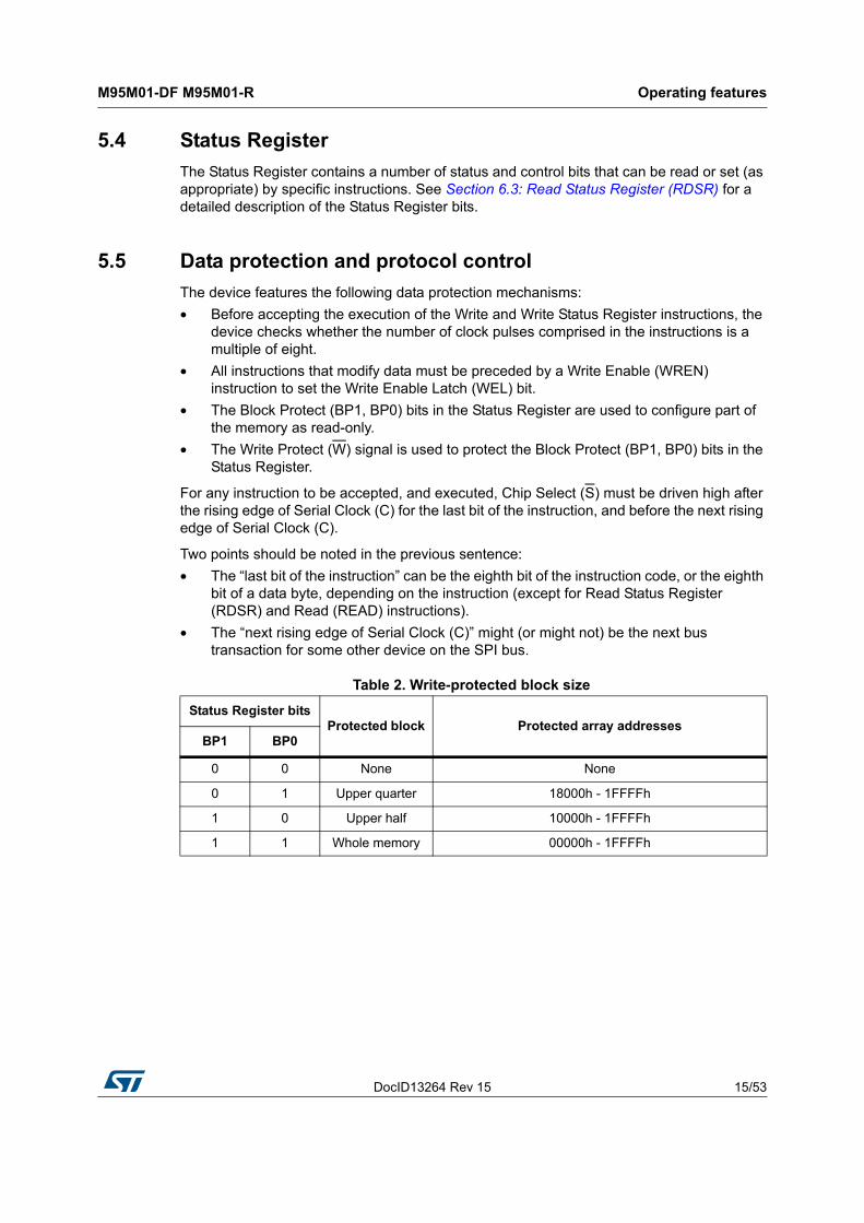
Table 2. Write-protected block size
Status Register bitsProtected block Protected array addresses
BP1 BP0
0 0 None None
0 1 Upper quarter 18000h - 1FFFFh
1 0 Upper half 10000h - 1FFFFh
1 1 Whole memory 00000h - 1FFFFh
Instructions M95M01-DF M95M01-R
16/53 DocID13264 Rev 15
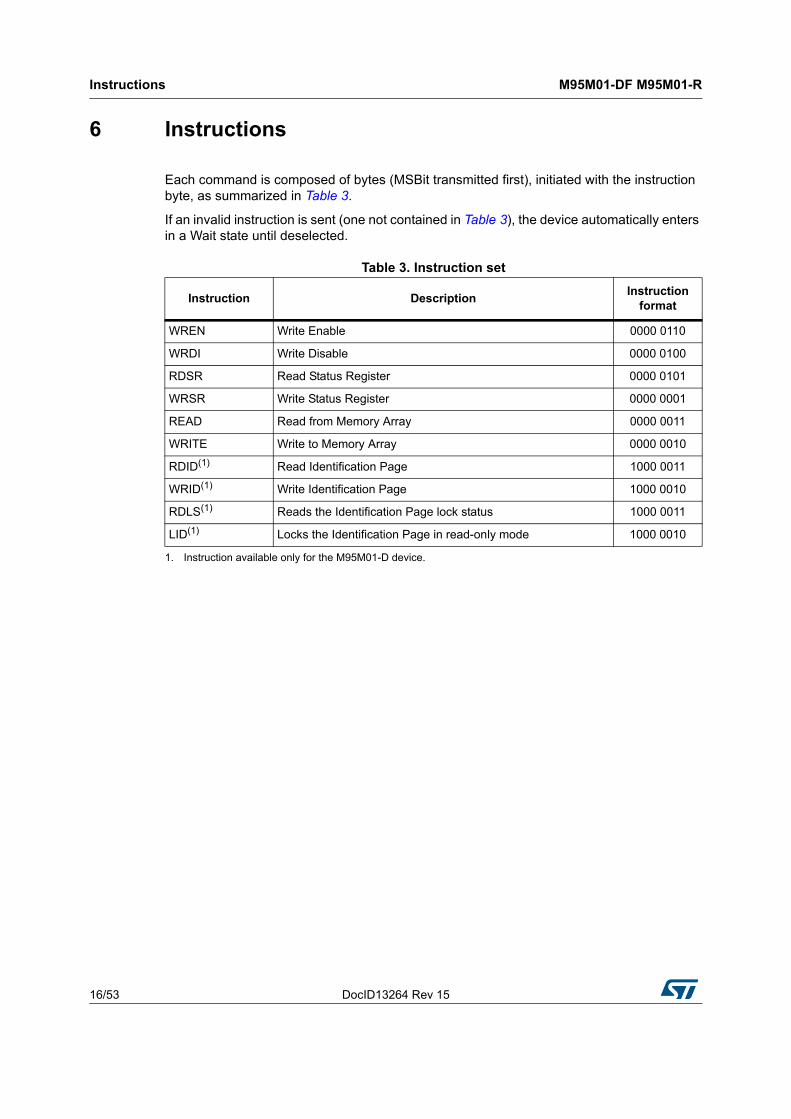
6 Instructions
Each command is composed of bytes (MSBit transmitted first), initiated with the instruction byte, as summarized in Table 3.
If an invalid instruction is sent (one not contained in Table 3), the device automatically enters in a Wait state until deselected.
Table 3. Instruction set
Instruction DescriptionInstruction
format
WREN Write Enable 0000 0110
WRDI Write Disable 0000 0100
RDSR Read Status Register 0000 0101
WRSR Write Status Register 0000 0001
READ Read from Memory Array 0000 0011
WRITE Write to Memory Array 0000 0010
RDID(1)
1. Instruction available only for the M95M01-D device.
Read Identification Page 1000 0011
WRID(1) Write Identification Page 1000 0010
RDLS(1) Reads the Identification Page lock status 1000 0011
LID(1) Locks the Identification Page in read-only mode 1000 0010
DocID13264 Rev 15 17/53
M95M01-DF M95M01-R Instructions
37
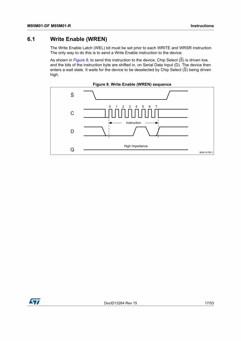
6.1 Write Enable (WREN)
The Write Enable Latch (WEL) bit must be set prior to each WRITE and WRSR instruction. The only way to do this is to send a Write Enable instruction to the device.
As shown in Figure 8, to send this instruction to the device, Chip Select (S) is driven low, and the bits of the instruction byte are shifted in, on Serial Data Input (D). The device then enters a wait state. It waits for the device to be deselected by Chip Select (S) being driven high.
Figure 8. Write Enable (WREN) sequence
Instructions M95M01-DF M95M01-R
18/53 DocID13264 Rev 15
6.2 Write Disable (WRDI)
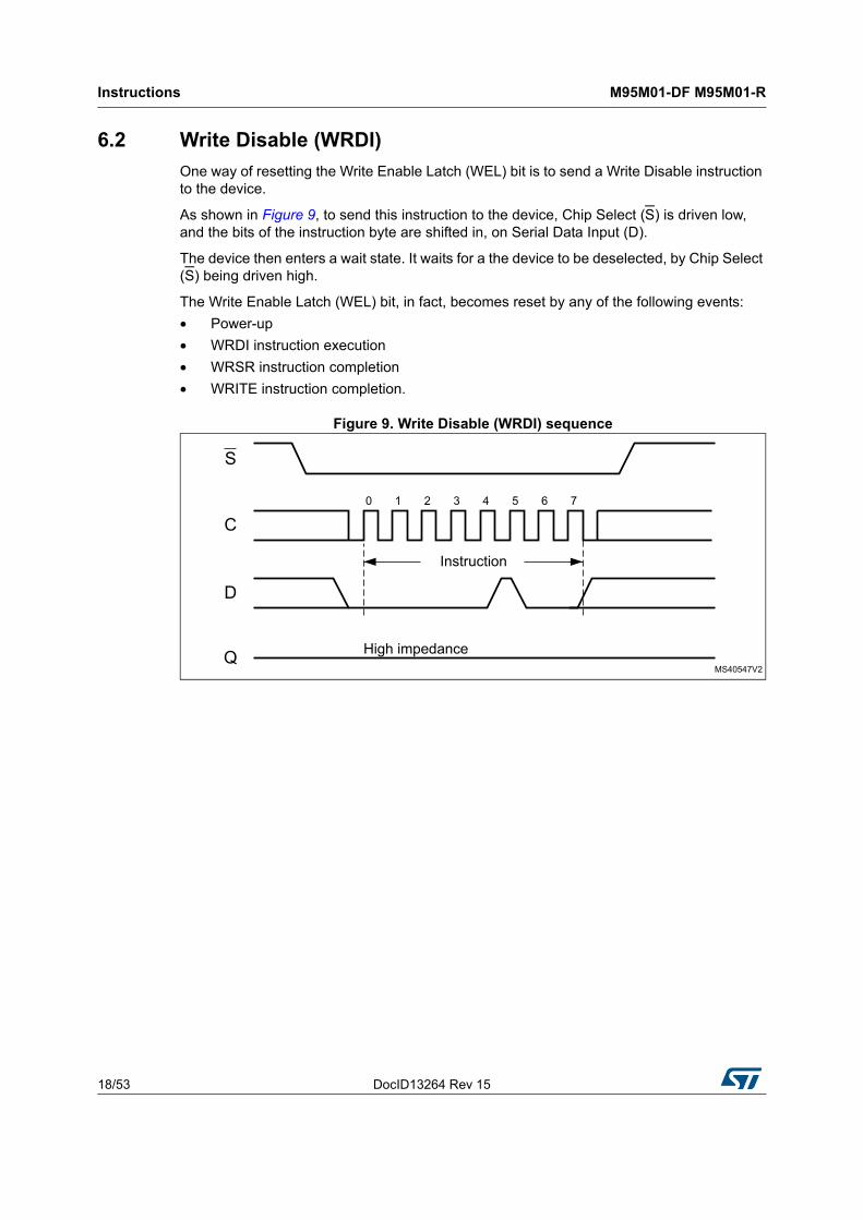
One way of resetting the Write Enable Latch (WEL) bit is to send a Write Disable instruction to the device.
As shown in Figure 9, to send this instruction to the device, Chip Select (S) is driven low, and the bits of the instruction byte are shifted in, on Serial Data Input (D).
The device then enters a wait state. It waits for a the device to be deselected, by Chip Select (S) being driven high.
The Write Enable Latch (WEL) bit, in fact, becomes reset by any of the following events:
• Power-up
• WRDI instruction execution
• WRSR instruction completion
• WRITE instruction completion.
Figure 9. Write Disable (WRDI) sequence
DocID13264 Rev 15 19/53
M95M01-DF M95M01-R Instructions
37
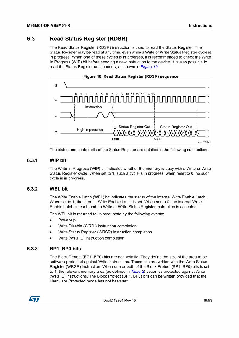
6.3 Read Status Register (RDSR)
The Read Status Register (RDSR) instruction is used to read the Status Register. The Status Register may be read at any time, even while a Write or Write Status Register cycle is in progress. When one of these cycles is in progress, it is recommended to check the Write In Progress (WIP) bit before sending a new instruction to the device. It is also possible to read the Status Register continuously, as shown in Figure 10.
Figure 10. Read Status Register (RDSR) sequence
The status and control bits of the Status Register are detailed in the following subsections.
6.3.1 WIP bit
The Write In Progress (WIP) bit indicates whether the memory is busy with a Write or Write Status Register cycle. When set to 1, such a cycle is in progress, when reset to 0, no such cycle is in progress.
6.3.2 WEL bit
The Write Enable Latch (WEL) bit indicates the status of the internal Write Enable Latch. When set to 1, the internal Write Enable Latch is set. When set to 0, the internal Write Enable Latch is reset, and no Write or Write Status Register instruction is accepted.
The WEL bit is returned to its reset state by the following events:
• Power-up
• Write Disable (WRDI) instruction completion
• Write Status Register (WRSR) instruction completion
• Write (WRITE) instruction completion
6.3.3 BP1, BP0 bits
The Block Protect (BP1, BP0) bits are non volatile. They define the size of the area to be software-protected against Write instructions. These bits are written with the Write Status Register (WRSR) instruction. When one or both of the Block Protect (BP1, BP0) bits is set to 1, the relevant memory area (as defined in Table 2) becomes protected against Write (WRITE) instructions. The Block Protect (BP1, BP0) bits can be written provided that the Hardware Protected mode has not been set.

Instructions M95M01-DF M95M01-R
20/53 DocID13264 Rev 15
6.3.4 SRWD bit
The Status Register Write Disable (SRWD) bit is operated in conjunction with the Write Protect (W) signal. The Status Register Write Disable (SRWD) bit and Write Protect (W) signal enable the device to be put in the Hardware Protected mode (when the Status Register Write Disable (SRWD) bit is set to 1, and Write Protect (W) is driven low). In this mode, the non-volatile bits of the Status Register (SRWD, BP1, BP0) become read-only bits and the Write Status Register (WRSR) instruction is no longer accepted for execution.
Table 4. Status Register format
b7 b0
SRWD 0 0 0 BP1 BP0 WEL WIP
Status Register Write Protect
Block Protect bits
Write Enable Latch bit
Write In Progress bit
DocID13264 Rev 15 21/53
M95M01-DF M95M01-R Instructions
37
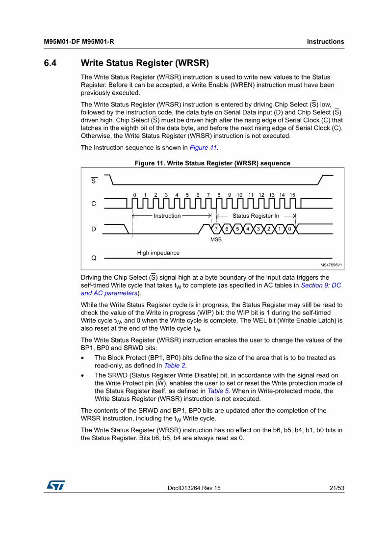
6.4 Write Status Register (WRSR)
The Write Status Register (WRSR) instruction is used to write new values to the Status Register. Before it can be accepted, a Write Enable (WREN) instruction must have been previously executed.
The Write Status Register (WRSR) instruction is entered by driving Chip Select (S) low, followed by the instruction code, the data byte on Serial Data input (D) and Chip Select (S) driven high. Chip Select (S) must be driven high after the rising edge of Serial Clock (C) that latches in the eighth bit of the data byte, and before the next rising edge of Serial Clock (C). Otherwise, the Write Status Register (WRSR) instruction is not executed.
The instruction sequence is shown in Figure 11.
Figure 11. Write Status Register (WRSR) sequence
Driving the Chip Select (S) signal high at a byte boundary of the input data triggers the self-timed Write cycle that takes tW to complete (as specified in AC tables in Section 9: DC and AC parameters).
While the Write Status Register cycle is in progress, the Status Register may still be read to check the value of the Write in progress (WIP) bit: the WIP bit is 1 during the self-timed Write cycle tW, and 0 when the Write cycle is complete. The WEL bit (Write Enable Latch) is also reset at the end of the Write cycle tW.
The Write Status Register (WRSR) instruction enables the user to change the values of the BP1, BP0 and SRWD bits:
• The Block Protect (BP1, BP0) bits define the size of the area that is to be treated as read-only, as defined in Table 2.
• The SRWD (Status Register Write Disable) bit, in accordance with the signal read on the Write Protect pin (W), enables the user to set or reset the Write protection mode of the Status Register itself, as defined in Table 5. When in Write-protected mode, the Write Status Register (WRSR) instruction is not executed.
The contents of the SRWD and BP1, BP0 bits are updated after the completion of the WRSR instruction, including the tW Write cycle.
The Write Status Register (WRSR) instruction has no effect on the b6, b5, b4, b1, b0 bits in the Status Register. Bits b6, b5, b4 are always read as 0.
Instructions M95M01-DF M95M01-R
22/53 DocID13264 Rev 15
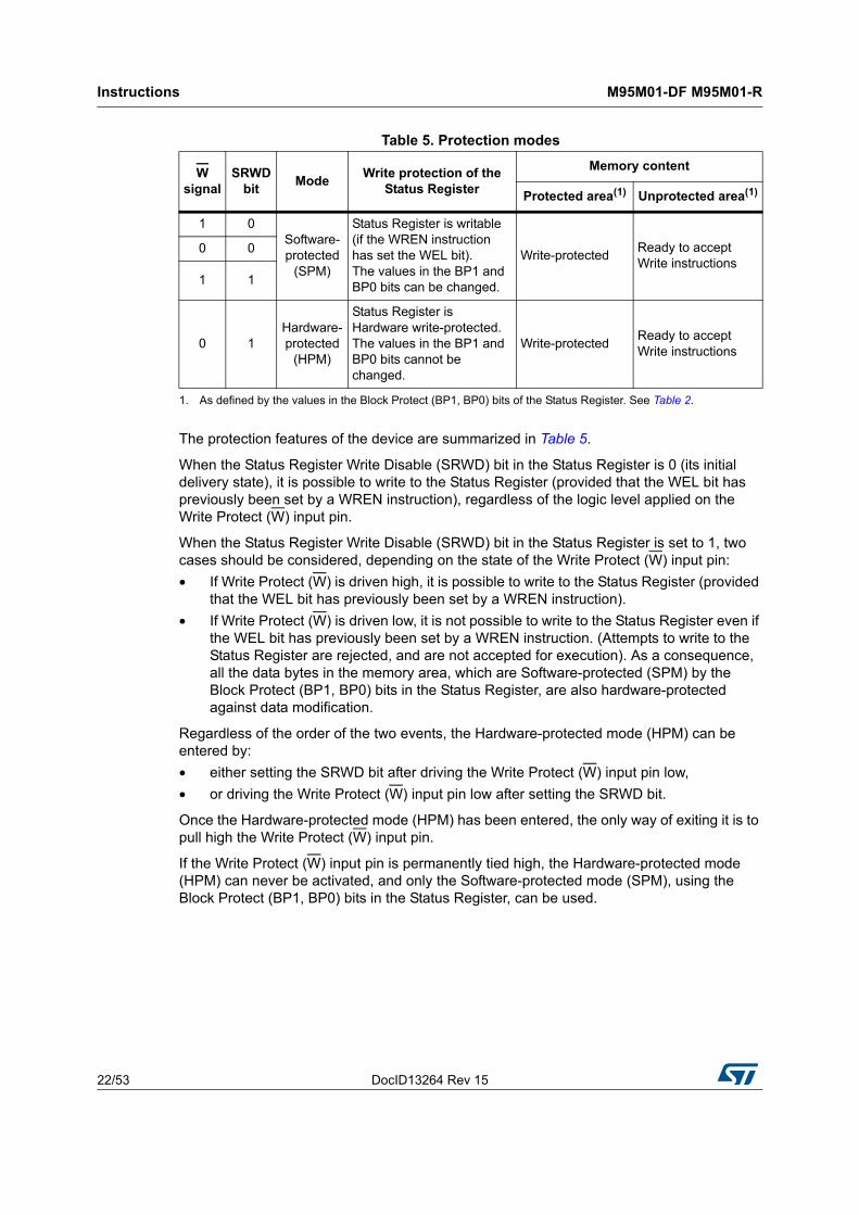
The protection features of the device are summarized in Table 5.
When the Status Register Write Disable (SRWD) bit in the Status Register is 0 (its initial delivery state), it is possible to write to the Status Register (provided that the WEL bit has previously been set by a WREN instruction), regardless of the logic level applied on the Write Protect (W) input pin.
When the Status Register Write Disable (SRWD) bit in the Status Register is set to 1, two cases should be considered, depending on the state of the Write Protect (W) input pin:
• If Write Protect (W) is driven high, it is possible to write to the Status Register (provided that the WEL bit has previously been set by a WREN instruction).
• If Write Protect (W) is driven low, it is not possible to write to the Status Register even if the WEL bit has previously been set by a WREN instruction. (Attempts to write to the Status Register are rejected, and are not accepted for execution). As a consequence, all the data bytes in the memory area, which are Software-protected (SPM) by the Block Protect (BP1, BP0) bits in the Status Register, are also hardware-protected against data modification.
Regardless of the order of the two events, the Hardware-protected mode (HPM) can be entered by:
• either setting the SRWD bit after driving the Write Protect (W) input pin low,
• or driving the Write Protect (W) input pin low after setting the SRWD bit.
Once the Hardware-protected mode (HPM) has been entered, the only way of exiting it is to pull high the Write Protect (W) input pin.
If the Write Protect (W) input pin is permanently tied high, the Hardware-protected mode (HPM) can never be activated, and only the Software-protected mode (SPM), using the Block Protect (BP1, BP0) bits in the Status Register, can be used.
Table 5. Protection modes
W signal
SRWD bit
ModeWrite protection of the
Status Register
Memory content
Protected area(1)
1. As defined by the values in the Block Protect (BP1, BP0) bits of the Status Register. See Table 2.
Unprotected area(1)
1 0Software-protected
(SPM)
Status Register is writable (if the WREN instruction has set the WEL bit). The values in the BP1 and BP0 bits can be changed.
Write-protectedReady to accept Write instructions
0 0
1 1
0 1Hardware-protected
(HPM)
Status Register is Hardware write-protected. The values in the BP1 and BP0 bits cannot be changed.
Write-protectedReady to accept Write instructions
DocID13264 Rev 15 23/53
M95M01-DF M95M01-R Instructions
37
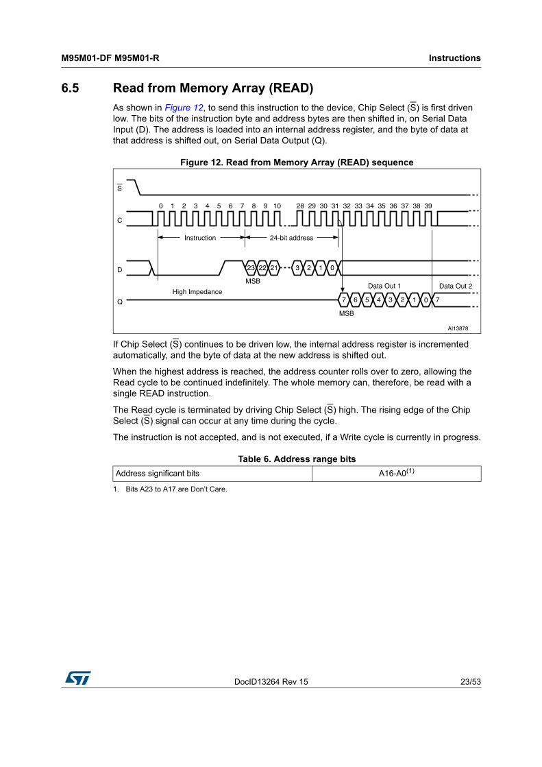
6.5 Read from Memory Array (READ)
As shown in Figure 12, to send this instruction to the device, Chip Select (S) is first driven low. The bits of the instruction byte and address bytes are then shifted in, on Serial Data Input (D). The address is loaded into an internal address register, and the byte of data at that address is shifted out, on Serial Data Output (Q).
Figure 12. Read from Memory Array (READ) sequence
If Chip Select (S) continues to be driven low, the internal address register is incremented automatically, and the byte of data at the new address is shifted out.
When the highest address is reached, the address counter rolls over to zero, allowing the Read cycle to be continued indefinitely. The whole memory can, therefore, be read with a single READ instruction.
The Read cycle is terminated by driving Chip Select (S) high. The rising edge of the Chip Select (S) signal can occur at any time during the cycle.
The instruction is not accepted, and is not executed, if a Write cycle is currently in progress.
Table 6. Address range bits
Address significant bits A16-A0(1)
1. Bits A23 to A17 are Don’t Care.
C
D
AI13878
S
Q
23
21 3 4 5 6 7 8 9 10 28 29 30 31 32 33 34 35
22 21 3 2 1 0
36 37 38
7 6 5 4 3 1 70High Impedance
Data Out 1
Instruction 24-bit address
0
MSB
MSB
2
39
Data Out 2
Instructions M95M01-DF M95M01-R
24/53 DocID13264 Rev 15
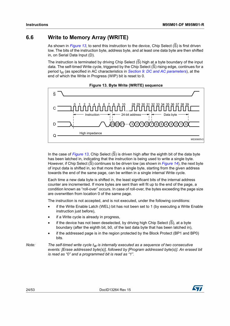
6.6 Write to Memory Array (WRITE)
As shown in Figure 13, to send this instruction to the device, Chip Select (S) is first driven low. The bits of the instruction byte, address byte, and at least one data byte are then shifted in, on Serial Data Input (D).
The instruction is terminated by driving Chip Select (S) high at a byte boundary of the input data. The self-timed Write cycle, triggered by the Chip Select (S) rising edge, continues for a period tW (as specified in AC characteristics in Section 9: DC and AC parameters), at the end of which the Write in Progress (WIP) bit is reset to 0.
Figure 13. Byte Write (WRITE) sequence
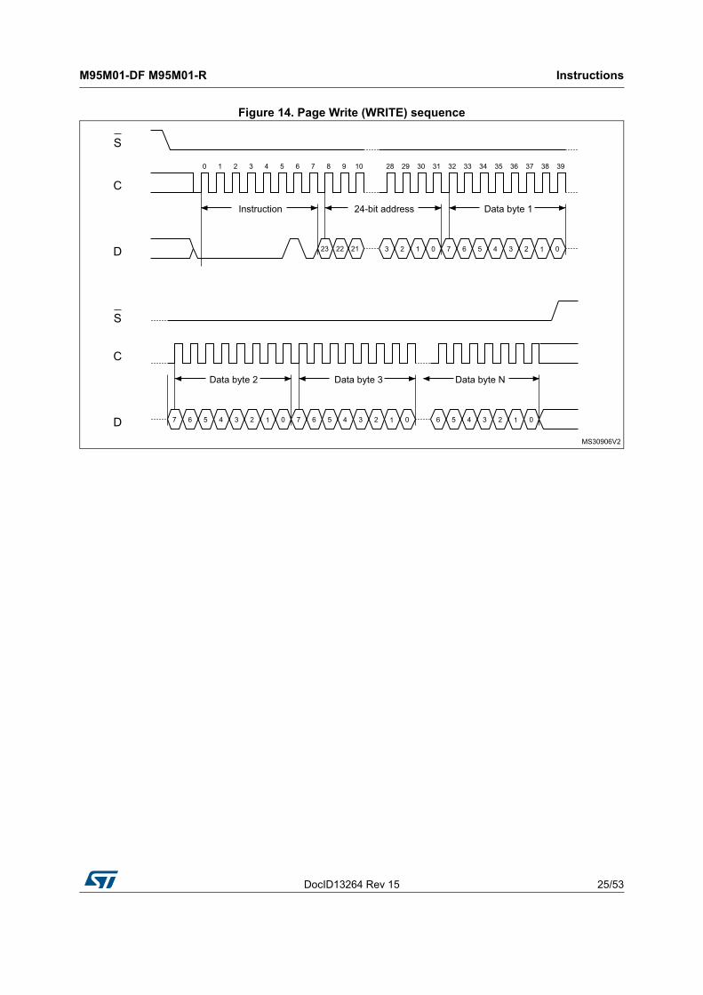
In the case of Figure 13, Chip Select (S) is driven high after the eighth bit of the data byte has been latched in, indicating that the instruction is being used to write a single byte. However, if Chip Select (S) continues to be driven low (as shown in Figure 14), the next byte of input data is shifted in, so that more than a single byte, starting from the given address towards the end of the same page, can be written in a single internal Write cycle.
Each time a new data byte is shifted in, the least significant bits of the internal address counter are incremented. If more bytes are sent than will fit up to the end of the page, a condition known as “roll-over” occurs. In case of roll-over, the bytes exceeding the page size are overwritten from location 0 of the same page.
The instruction is not accepted, and is not executed, under the following conditions:
• if the Write Enable Latch (WEL) bit has not been set to 1 (by executing a Write Enable instruction just before),
• if a Write cycle is already in progress,
• if the device has not been deselected, by driving high Chip Select (S), at a byte boundary (after the eighth bit, b0, of the last data byte that has been latched in),
• if the addressed page is in the region protected by the Block Protect (BP1 and BP0) bits.
Note: The self-timed write cycle tW is internally executed as a sequence of two consecutive events: [Erase addressed byte(s)], followed by [Program addressed byte(s)]. An erased bit is read as “0” and a programmed bit is read as “1”.
DocID13264 Rev 15 25/53
M95M01-DF M95M01-R Instructions
37
Figure 14. Page Write (WRITE) sequence
Instructions M95M01-DF M95M01-R
26/53 DocID13264 Rev 15
6.6.1 Cycling with Error Correction Code (ECC)
The ECC is an internal logic function transparent for the SPI communication protocol.
The ECC logic is implemented on each group of four EEPROM bytes(a). Inside a group, if a single bit out of the four bytes happens to be erroneous during a Read operation, the ECC detects this bit and replaces it with the correct value. The read reliability is therefore much improved.
Even if the ECC function is performed on groups of four bytes, a single byte can be written/cycled independently. In this case, the ECC function also writes/cycles the three other bytes located in the same group(a). As a consequence, the maximum cycling budget is defined at group level and the cycling can be distributed over the four bytes of the group: the sum of the cycles seen by byte0, byte1, byte2 and byte3 of the same group must remain below the maximum value defined in Table 11.
a. A group of four bytes is located at addresses [4*N, 4*N+1, 4*N+2, 4*N+3], where N is an integer.
DocID13264 Rev 15 27/53
M95M01-DF M95M01-R Instructions
37
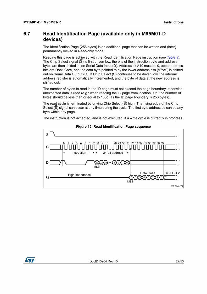
6.7 Read Identification Page (available only in M95M01-D devices)
The Identification Page (256 bytes) is an additional page that can be written and (later) permanently locked in Read-only mode.
Reading this page is achieved with the Read Identification Page instruction (see Table 3). The Chip Select signal (S) is first driven low, the bits of the instruction byte and address bytes are then shifted in, on Serial Data Input (D). Address bit A10 must be 0, upper address bits are Don't Care, and the data byte pointed to by the lower address bits [A7:A0] is shifted out on Serial Data Output (Q). If Chip Select (S) continues to be driven low, the internal address register is automatically incremented, and the byte of data at the new address is shifted out.
The number of bytes to read in the ID page must not exceed the page boundary, otherwise unexpected data is read (e.g.: when reading the ID page from location 90d, the number of bytes should be less than or equal to 166d, as the ID page boundary is 256 bytes).
The read cycle is terminated by driving Chip Select (S) high. The rising edge of the Chip Select (S) signal can occur at any time during the cycle. The first byte addressed can be any byte within any page.
The instruction is not accepted, and is not executed, if a write cycle is currently in progress.
Figure 15. Read Identification Page sequence
Instructions M95M01-DF M95M01-R
28/53 DocID13264 Rev 15
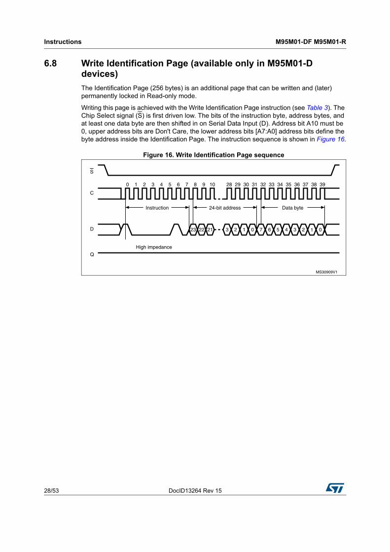
6.8 Write Identification Page (available only in M95M01-D devices)
The Identification Page (256 bytes) is an additional page that can be written and (later) permanently locked in Read-only mode.
Writing this page is achieved with the Write Identification Page instruction (see Table 3). The Chip Select signal (S) is first driven low. The bits of the instruction byte, address bytes, and at least one data byte are then shifted in on Serial Data Input (D). Address bit A10 must be 0, upper address bits are Don't Care, the lower address bits [A7:A0] address bits define the byte address inside the Identification Page. The instruction sequence is shown in Figure 16.
Figure 16. Write Identification Page sequence
DocID13264 Rev 15 29/53
M95M01-DF M95M01-R Instructions
37
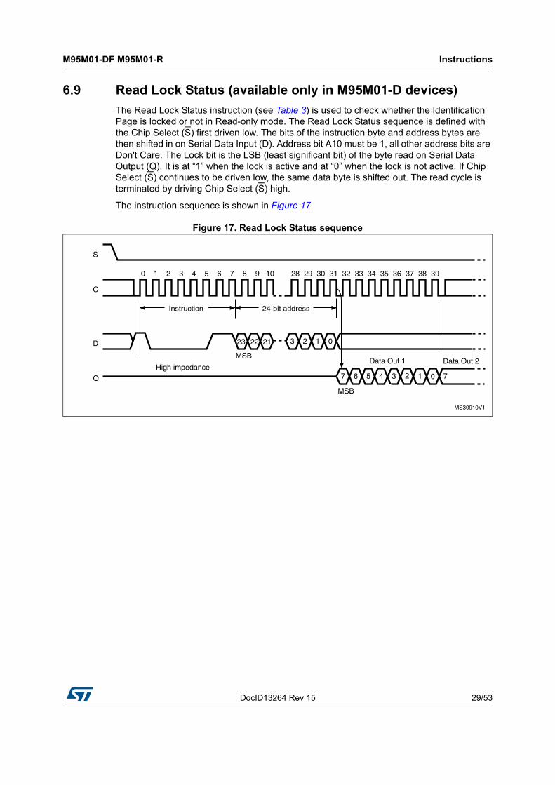
6.9 Read Lock Status (available only in M95M01-D devices)
The Read Lock Status instruction (see Table 3) is used to check whether the Identification Page is locked or not in Read-only mode. The Read Lock Status sequence is defined with the Chip Select (S) first driven low. The bits of the instruction byte and address bytes are then shifted in on Serial Data Input (D). Address bit A10 must be 1, all other address bits are Don't Care. The Lock bit is the LSB (least significant bit) of the byte read on Serial Data Output (Q). It is at “1” when the lock is active and at “0” when the lock is not active. If Chip Select (S) continues to be driven low, the same data byte is shifted out. The read cycle is terminated by driving Chip Select (S) high.
The instruction sequence is shown in Figure 17.
Figure 17. Read Lock Status sequence
Instructions M95M01-DF M95M01-R
30/53 DocID13264 Rev 15
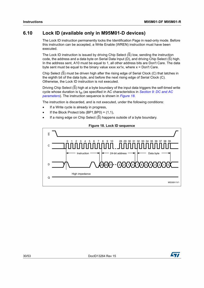
6.10 Lock ID (available only in M95M01-D devices)
The Lock ID instruction permanently locks the Identification Page in read-only mode. Before this instruction can be accepted, a Write Enable (WREN) instruction must have been executed.
The Lock ID instruction is issued by driving Chip Select (S) low, sending the instruction code, the address and a data byte on Serial Data Input (D), and driving Chip Select (S) high. In the address sent, A10 must be equal to 1, all other address bits are Don't Care. The data byte sent must be equal to the binary value xxxx xx1x, where x = Don't Care.
Chip Select (S) must be driven high after the rising edge of Serial Clock (C) that latches in the eighth bit of the data byte, and before the next rising edge of Serial Clock (C). Otherwise, the Lock ID instruction is not executed.
Driving Chip Select (S) high at a byte boundary of the input data triggers the self-timed write cycle whose duration is tW (as specified in AC characteristics in Section 9: DC and AC parameters). The instruction sequence is shown in Figure 18.
The instruction is discarded, and is not executed, under the following conditions:
• If a Write cycle is already in progress,
• If the Block Protect bits (BP1,BP0) = (1,1),
• If a rising edge on Chip Select (S) happens outside of a byte boundary.
Figure 18. Lock ID sequence

DocID13264 Rev 15 31/53
M95M01-DF M95M01-R Power-up and delivery state
37
7 Power-up and delivery state
7.1 Power-up state
After power-up, the device is in the following state:
• Standby power mode,
• deselected (after power-up, a falling edge is required on Chip Select (S) before any instructions can be started),
• not in the Hold condition,
• the Write Enable Latch (WEL) is reset to 0,
• Write In Progress (WIP) is reset to 0.
The SRWD, BP1 and BP0 bits of the Status Register are unchanged from the previous power-down (they are non-volatile bits).
7.2 Initial delivery state
The device is delivered with the memory array bits and Identification Page bits set to all 1s (each byte = FFh). The Status Register Write Disable (SRWD) and Block Protect (BP1 and BP0) bits are initialized to 0.
Maximum ratings M95M01-DF M95M01-R
32/53 DocID13264 Rev 15
8 Maximum ratings
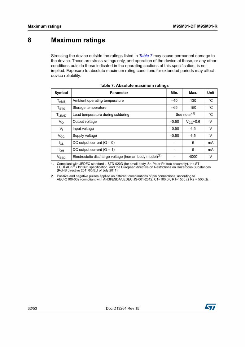
Stressing the device outside the ratings listed in Table 7 may cause permanent damage to the device. These are stress ratings only, and operation of the device at these, or any other conditions outside those indicated in the operating sections of this specification, is not implied. Exposure to absolute maximum rating conditions for extended periods may affect device reliability.
Table 7. Absolute maximum ratings
Symbol Parameter Min. Max. Unit
TAMB Ambient operating temperature –40 130 °C
TSTG Storage temperature –65 150 °C
TLEAD Lead temperature during soldering See note (1)
1. Compliant with JEDEC standard J-STD-020D (for small-body, Sn-Pb or Pb free assembly), the ST ECOPACK® 7191395 specification, and the European directive on Restrictions on Hazardous Substances (RoHS directive 2011/65/EU of July 2011).
°C
VO Output voltage –0.50 VCC+0.6 V
VI Input voltage –0.50 6.5 V
VCC Supply voltage –0.50 6.5 V
IOL DC output current (Q = 0) - 5 mA
IOH DC output current (Q = 1) - 5 mA
VESD Electrostatic discharge voltage (human body model)(2)
2. Positive and negative pulses applied on different combinations of pin connections, according to AEC-Q100-002 (compliant with ANSI/ESDA/JEDEC JS-001-2012, C1=100 pF, R1=1500 Ω, R2 = 500 Ω).
- 4000 V

DocID13264 Rev 15 33/53
M95M01-DF M95M01-R DC and AC parameters
37
9 DC and AC parameters
This section summarizes the operating conditions and the DC/AC characteristics.
Figure 19. AC measurement I/O waveform
Table 8. Operating conditions (M95M01-R, device grade 6)
Symbol Parameter Min. Max. Unit
VCC Supply voltage 1.8 5.5 V
TA Ambient operating temperature –40 85 °C
Table 9. Operating conditions (M95M01-DF, device grade 6)
Symbol Parameter Min. Max. Unit
VCC Supply voltage 1.7 5.5 V
TA Ambient operating temperature –40 85 °C
Table 10. AC measurement conditions
Symbol Parameter Min. Max. Unit
CL Load capacitance - 100 pF
- Input rise and fall times - 50 ns
- Input pulse voltages 0.2 VCC to 0.8 VCC V
- Input and output timing reference voltages 0.3 VCC to 0.7 VCC V
DC and AC parameters M95M01-DF M95M01-R
34/53 DocID13264 Rev 15
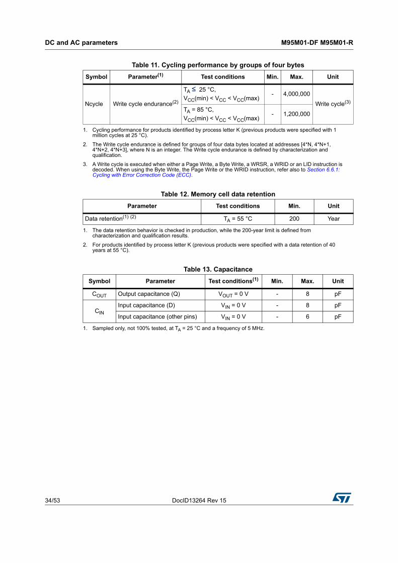
Table 11. Cycling performance by groups of four bytes
Symbol Parameter(1)
1. Cycling performance for products identified by process letter K (previous products were specified with 1 million cycles at 25 °C).
Test conditions Min. Max. Unit
Ncycle Write cycle endurance(2)
2. The Write cycle endurance is defined for groups of four data bytes located at addresses [4*N, 4*N+1, 4*N+2, 4*N+3], where N is an integer. The Write cycle endurance is defined by characterization and qualification.
TA ≤ 25 °C,
VCC(min) < VCC < VCC(max)- 4,000,000
Write cycle(3)
3. A Write cycle is executed when either a Page Write, a Byte Write, a WRSR, a WRID or an LID instruction is decoded. When using the Byte Write, the Page Write or the WRID instruction, refer also to Section 6.6.1: Cycling with Error Correction Code (ECC).
TA = 85 °C,
VCC(min) < VCC < VCC(max)- 1,200,000
Table 12. Memory cell data retention
Parameter Test conditions Min. Unit
Data retention(1) (2)
1. The data retention behavior is checked in production, while the 200-year limit is defined from characterization and qualification results.
2. For products identified by process letter K (previous products were specified with a data retention of 40 years at 55 °C).
TA = 55 °C 200 Year
Table 13. Capacitance
Symbol Parameter Test conditions(1)
1. Sampled only, not 100% tested, at TA = 25 °C and a frequency of 5 MHz.
Min. Max. Unit
COUT Output capacitance (Q) VOUT = 0 V - 8 pF
CIN
Input capacitance (D) VIN = 0 V - 8 pF
Input capacitance (other pins) VIN = 0 V - 6 pF

DocID13264 Rev 15 35/53
M95M01-DF M95M01-R DC and AC parameters
37
Table 14. DC characteristics
Symbol Parameter Test conditions Min Max Unit
ILI Input leakage current VIN = VSS or VCC - ± 2 µA
ILO Output leakage current S = VCC, VOUT = VSS or VCC - ± 2 µA
ICC Supply current (Read)
C = 0.1 VCC/0.9 VCC at 2 MHz, VCC = 1.8 V(1), Q = open
- 1.5 mA
C = 0.1 VCC/0.9 VCC at 5 MHz, VCC = 1.8 V(1), Q = open
- 2(2) mA
C = 0.1 VCC/0.9 VCC at 5 MHz, VCC = 2.5 V, Q = open
- 4 mA
C = 0.1 VCC/0.9 VCC at 10 MHz, VCC = 2.5 V, Q = open
- 2(2) mA
C = 0.1 VCC/0.9 VCC at 5 MHz, VCC = 5 V, Q = open
- 5 mA
C = 0.1 VCC/0.9 VCC at 10 MHz, VCC = 5.5 V, Q = open
- 5(2) mA
ICC0(3) Supply current (Write) During tW, S = VCC, - 5 mA
ICC1Supply current
(Standby Power mode)
S = VCC, VIN = VSS or VCC, VCC = 1.8 V(1) - 3 µA
S = VCC, VIN = VSS or VCC, VCC = 1.8 V(1), temp = 25 °C (or less)
- 1 µA
S = VCC, VIN = VSS or VCC, VCC = 2.5 V
- 3 µA
S = VCC, VIN = VSS or VCC, VCC = 2.5 V, temp = 25 °C (or less)
- 1 µA
S = VCC, VIN = VSS or VCC, VCC = 5.5 V
- 5 µA
S = VCC, VIN = VSS or VCC, VCC = 5.5 V, temp = 25 °C (or less)
- 1.5 µA
VIL Input low voltage1.8 V(1) ≤ VCC < 2.5 V –0.45 0.25 VCC
V2.5 V ≤ VCC ≤ 5.5 V –0.45 0.3 VCC
VIH Input high voltage1.8 V(1) ≤ VCC < 2.5 V 0.75 VCC VCC + 1
V2.5 V ≤ VCC ≤ 5.5 V 0.7 VCC VCC + 1
VOL Output low voltage
IOL = 0.15 mA, VCC = 1.8 V(1) - 0.3 V
VCC = 2.5 V, IOL = 1.5 mA or VCC = 5 V, IOL = 2 mA
- 0.4 V
VOH Output high voltage
IOH = –0.1 mA, VCC = 1.8 V(1)
0.8 VCC - VVCC = 2.5 V, IOH = –0.4 mA or VCC = 5 V, IOH = -2 mA
1. Or VCC = 1.7 V for the M95M01-DF.
2. For devices identified by process letter K.
3. Characterized value, not tested in production.
DC and AC parameters M95M01-DF M95M01-R
36/53 DocID13264 Rev 15
Table 15. AC characteristics
Test conditions specified in Table 8, Table 9 and Table 10
Symbol Alt. Parameter
VCC ≥ 1.7 V(1)
VCC ≥ 1.8 V(2)
VCC ≥ 2.5 V(3)
VCC ≥ 4.5 V(1)
Unit
Min. Max. Min. Max. Min. Max. Min. Max.
fC fSCK Clock frequency DC 2 DC 5 DC 10 DC 16 MHz
tSLCH tCSS1 S active setup time 150 - 60 - 30 - 20 - ns
tSHCH tCSS2 S not active setup time 150 - 60 - 30 - 20 - ns
tSHSL tCS S Deselect time 200 - 60 - 40 - 25 - ns
tCHSH tCSH S active hold time 150 - 60 - 30 - 20 - ns
tCHSL - S not active hold time 150 - 60 - 30 - 20 - ns
tCH(4) tCLH Clock high time 200 - 90 - 40 - 25 - ns
tCL(4) tCLL Clock low time 200 - 90 - 40 - 25 - ns
tCLCH(5) tRC Clock rise time - 2 - 2 - - - 2 µs
tCHCL(5) tFC Clock fall time - 2 - 2 - - - 2 µs
tDVCH tDSU Data in setup time 50 - 20 - 10 - 10 - ns
tCHDX tDH Data in hold time 50 - 20 - 10 - 10 - ns
tHHCH -Clock low hold time after HOLD not active
150 - 60 - 30 - 25 - ns
tHLCH -Clock low hold time after HOLD active
150 - 60 - 30 - 20 - ns
tCLHL -Clock low set-up time before HOLD active
0 - 0 - 0 - 0 - ns
tCLHH -Clock low set-up time before HOLD not active
0 - 0 - 0 - 0 - ns
tSHQZ(5) tDIS Output disable time - 200 - 80 - 40 - 25 ns
tCLQV tV Clock low to output valid - 200 - 80 - 40 - 25 ns
tCLQX tHO Output hold time 0 - 0 - 0 - 0 - ns
tQLQH(5) tRO Output rise time - 200 - 80 - 40 - 25 ns
tQHQL(5) tFO Output fall time - 200 - 80 - 40 - 25 ns
tHHQV tLZ HOLD high to output valid - 200 - 80 - 40 - 25 ns
tHLQZ(5) tHZ HOLD low to output high-Z - 200 - 80 - 40 - 25 ns
tW tWC Write time - 5 - 5 - 5 - 5 ms
1. For devices identified by process letter K.
2. Previous products (identified with process letter A) were specified with fC(max) = 2 MHz, with the same AC values as defined in the 1.7 V columns in this table.
3. Previous products (identified with process letter A) were specified with fC(max) = 5 MHz, with the same AC values as defined in the 1.8 V columns in this table.
4. tCH + tCL must never be less than the shortest possible clock period, 1 / fC(max)
5. Value guaranteed by characterization, not 100% tested in production.

DocID13264 Rev 15 37/53
M95M01-DF M95M01-R DC and AC parameters
37
Figure 20. Serial input timing
Figure 21. Hold timing
Figure 22. Serial output timing
Package information M95M01-DF M95M01-R
38/53 DocID13264 Rev 15
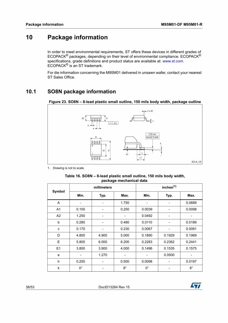
10 Package information
In order to meet environmental requirements, ST offers these devices in different grades of ECOPACK® packages, depending on their level of environmental compliance. ECOPACK® specifications, grade definitions and product status are available at: www.st.com. ECOPACK® is an ST trademark.
For die information concerning the M95M01 delivered in unsawn wafer, contact your nearest ST Sales Office.
10.1 SO8N package information
Figure 23. SO8N – 8-lead plastic small outline, 150 mils body width, package outline
1. Drawing is not to scale.
Table 16. SO8N – 8-lead plastic small outline, 150 mils body width,package mechanical data
Symbolmillimeters inches(1)
Min. Typ. Max. Min. Typ. Max.
A - - 1.750 - - 0.0689
A1 0.100 - 0.250 0.0039 - 0.0098
A2 1.250 - - 0.0492 - -
b 0.280 - 0.480 0.0110 - 0.0189
c 0.170 - 0.230 0.0067 - 0.0091
D 4.800 4.900 5.000 0.1890 0.1929 0.1969
E 5.800 6.000 6.200 0.2283 0.2362 0.2441
E1 3.800 3.900 4.000 0.1496 0.1535 0.1575
e - 1.270 - - 0.0500 -
h 0.250 - 0.500 0.0098 - 0.0197
k 0° - 8° 0° - 8°
DocID13264 Rev 15 39/53
M95M01-DF M95M01-R Package information
52
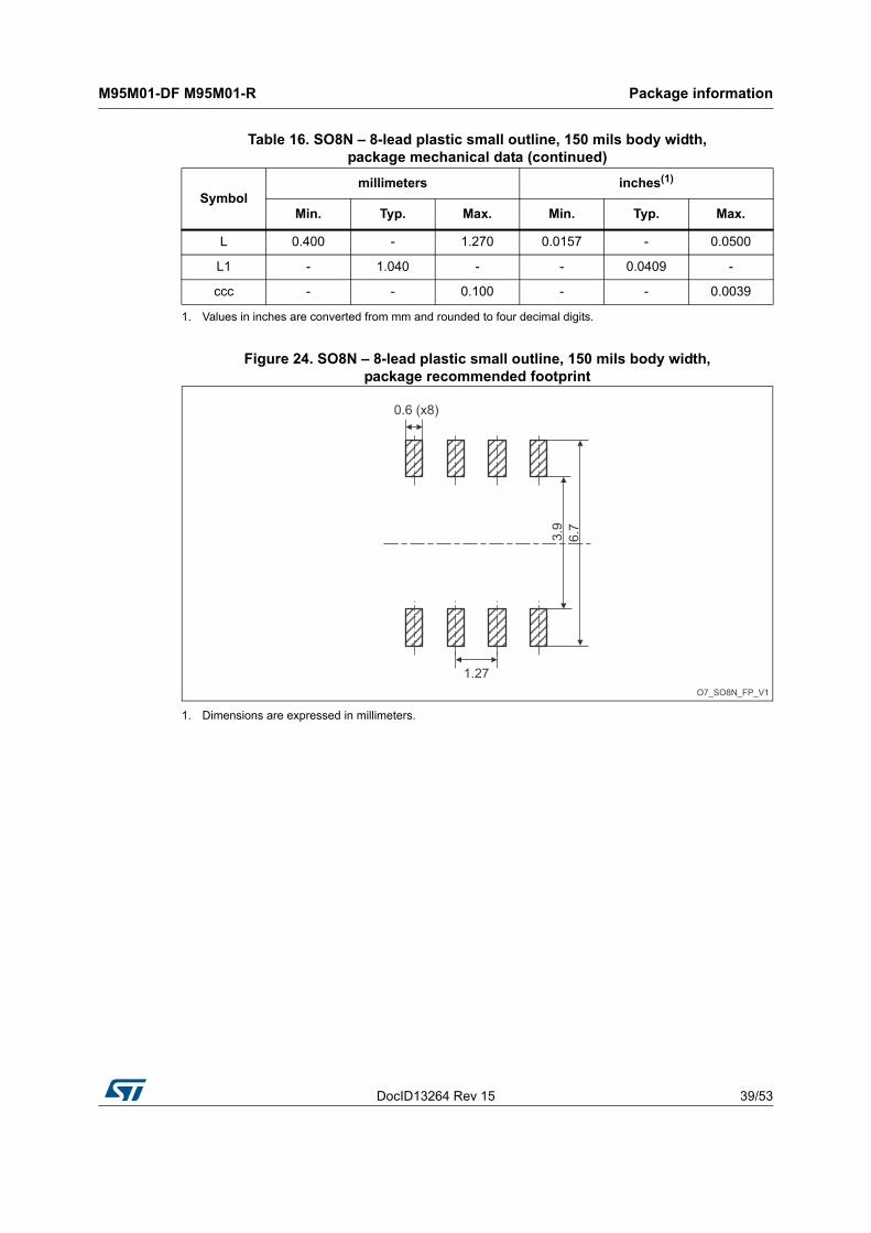
Figure 24. SO8N – 8-lead plastic small outline, 150 mils body width,package recommended footprint
1. Dimensions are expressed in millimeters.
L 0.400 - 1.270 0.0157 - 0.0500
L1 - 1.040 - - 0.0409 -
ccc - - 0.100 - - 0.0039
1. Values in inches are converted from mm and rounded to four decimal digits.
Table 16. SO8N – 8-lead plastic small outline, 150 mils body width,package mechanical data (continued)
Symbolmillimeters inches(1)
Min. Typ. Max. Min. Typ. Max.
Package information M95M01-DF M95M01-R
40/53 DocID13264 Rev 15
10.2 TSSOP8 package information
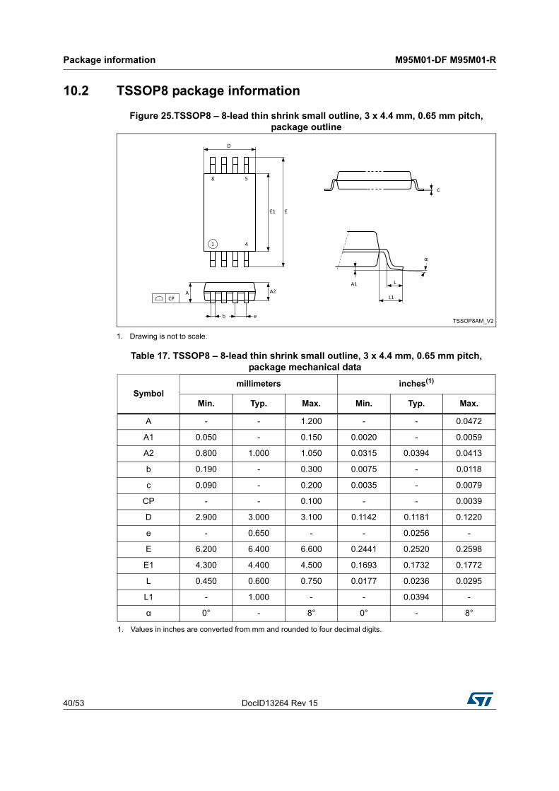
Figure 25.TSSOP8 – 8-lead thin shrink small outline, 3 x 4.4 mm, 0.65 mm pitch,package outline
1. Drawing is not to scale.
Table 17. TSSOP8 – 8-lead thin shrink small outline, 3 x 4.4 mm, 0.65 mm pitch,package mechanical data
Symbolmillimeters inches(1)
1. Values in inches are converted from mm and rounded to four decimal digits.
Min. Typ. Max. Min. Typ. Max.
A - - 1.200 - - 0.0472
A1 0.050 - 0.150 0.0020 - 0.0059
A2 0.800 1.000 1.050 0.0315 0.0394 0.0413
b 0.190 - 0.300 0.0075 - 0.0118
c 0.090 - 0.200 0.0035 - 0.0079
CP - - 0.100 - - 0.0039
D 2.900 3.000 3.100 0.1142 0.1181 0.1220
e - 0.650 - - 0.0256 -
E 6.200 6.400 6.600 0.2441 0.2520 0.2598
E1 4.300 4.400 4.500 0.1693 0.1732 0.1772
L 0.450 0.600 0.750 0.0177 0.0236 0.0295
L1 - 1.000 - - 0.0394 -
α 0° - 8° 0° - 8°
DocID13264 Rev 15 41/53
M95M01-DF M95M01-R Package information
52
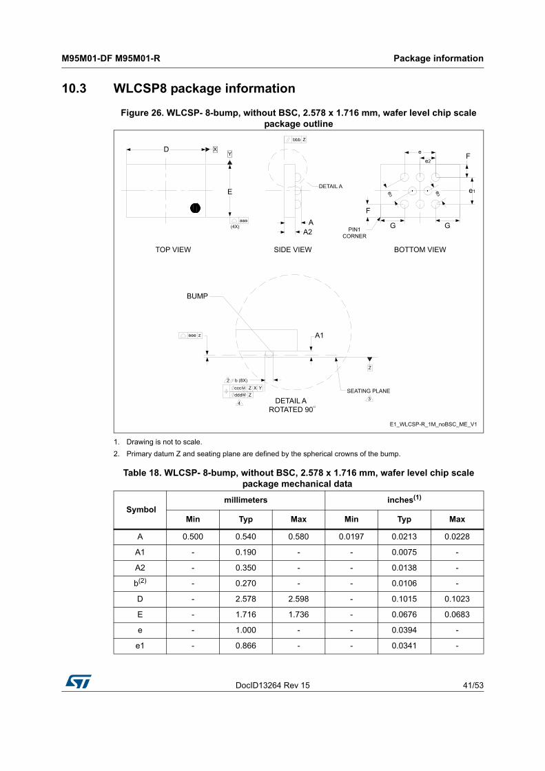
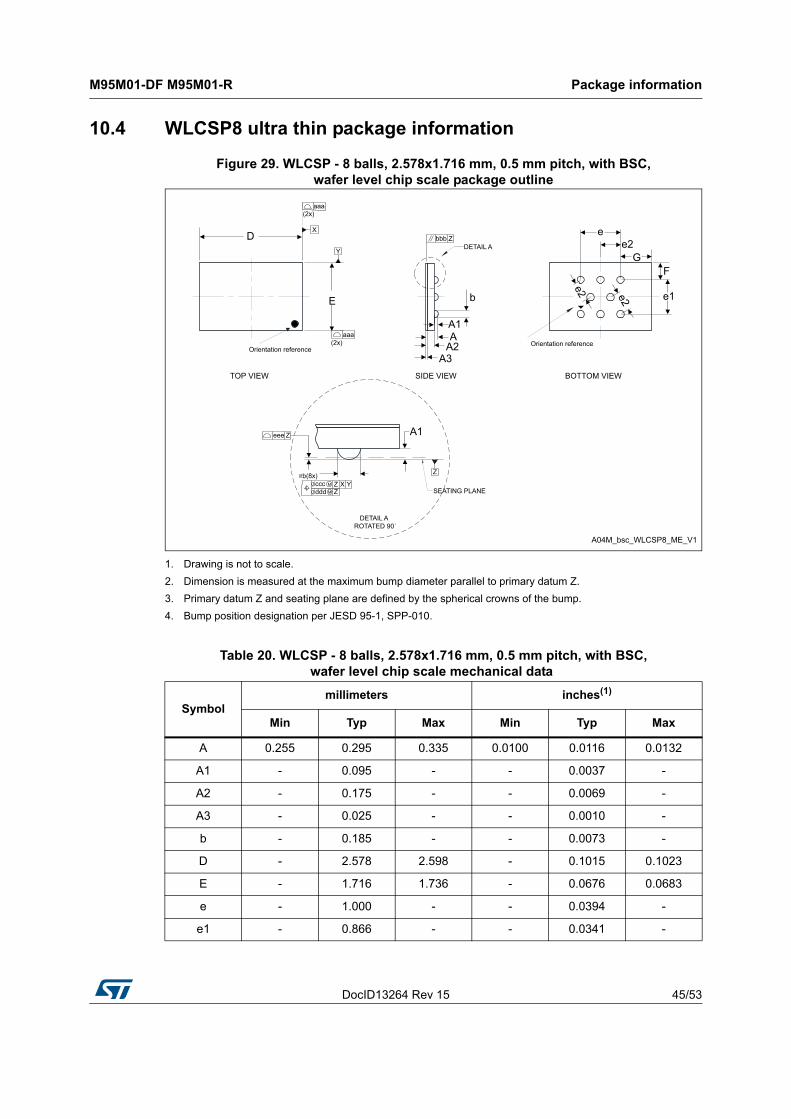
10.3 WLCSP8 package information
Figure 26. WLCSP- 8-bump, without BSC, 2.578 x 1.716 mm, wafer level chip scalepackage outline
1. Drawing is not to scale.
2. Primary datum Z and seating plane are defined by the spherical crowns of the bump.
Table 18. WLCSP- 8-bump, without BSC, 2.578 x 1.716 mm, wafer level chip scalepackage mechanical data
Symbolmillimeters inches(1)
Min Typ Max Min Typ Max
A 0.500 0.540 0.580 0.0197 0.0213 0.0228
A1 - 0.190 - - 0.0075 -
A2 - 0.350 - - 0.0138 -
b(2) - 0.270 - - 0.0106 -
D - 2.578 2.598 - 0.1015 0.1023
E - 1.716 1.736 - 0.0676 0.0683
e - 1.000 - - 0.0394 -
e1 - 0.866 - - 0.0341 -
Package information M95M01-DF M95M01-R
42/53 DocID13264 Rev 15
e2 - 0.500 - - 0.0197 -
e3 - 0.500 - - 0.0197 -
F - 0.425 - - 0.0167 -
G - 0.789 - - 0.0311 -
aaa - 0.110 - - 0.0043 -
bbb - 0.110 - - 0.0043 -
ccc - 0.110 - - 0.0043 -
ddd - 0.060 - - 0.0024 -
eee - 0.060 - - 0.0024 -
1. Values in inches are converted from mm and rounded to 4 decimal digits.
2. Dimension is measured at the maximum bump diameter parallel to primary datum Z.
Table 18. WLCSP- 8-bump, without BSC, 2.578 x 1.716 mm, wafer level chip scalepackage mechanical data (continued)
Symbolmillimeters inches(1)
Min Typ Max Min Typ Max
DocID13264 Rev 15 43/53
M95M01-DF M95M01-R Package information
52
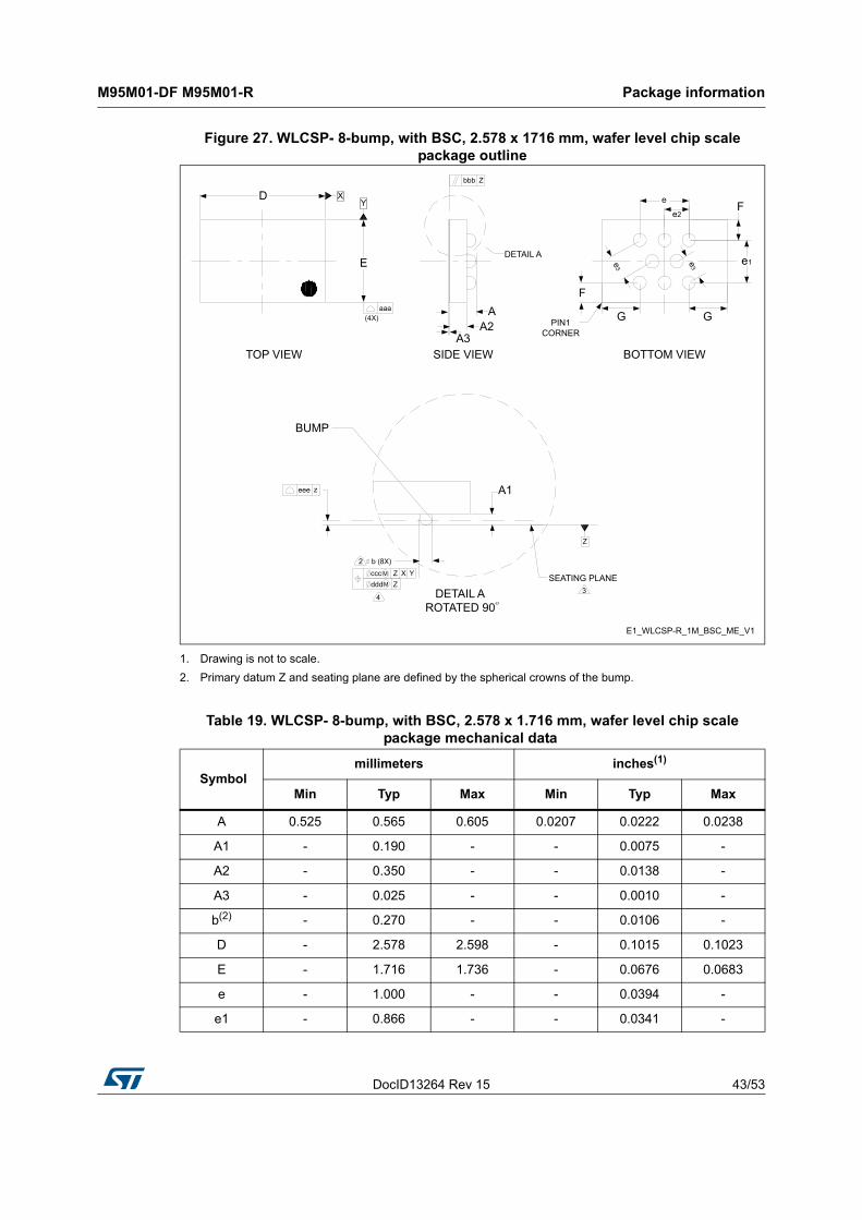
Figure 27. WLCSP- 8-bump, with BSC, 2.578 x 1716 mm, wafer level chip scalepackage outline
1. Drawing is not to scale.
2. Primary datum Z and seating plane are defined by the spherical crowns of the bump.
Table 19. WLCSP- 8-bump, with BSC, 2.578 x 1.716 mm, wafer level chip scalepackage mechanical data
Symbolmillimeters inches(1)
Min Typ Max Min Typ Max
A 0.525 0.565 0.605 0.0207 0.0222 0.0238
A1 - 0.190 - - 0.0075 -
A2 - 0.350 - - 0.0138 -
A3 - 0.025 - - 0.0010 -
b(2) - 0.270 - - 0.0106 -
D - 2.578 2.598 - 0.1015 0.1023
E - 1.716 1.736 - 0.0676 0.0683
e - 1.000 - - 0.0394 -
e1 - 0.866 - - 0.0341 -
Package information M95M01-DF M95M01-R
44/53 DocID13264 Rev 15
Figure 28. WLCSP- 8-bump, 2.578 x 1.716 mm, wafer level chip scale package recommended footprint
1. Dimensions are expressed in millimeters.
e2 - 0.500 - - 0.0197 -
e3 - 0.500 - - 0.0197 -
F - 0.425 - - 0.0167 -
G - 0.789 - - 0.0311 -
aaa - 0.110 - - 0.0043 -
bbb - 0.110 - - 0.0043 -
ccc - 0.110 - - 0.0043 -
ddd - 0.060 - - 0.0024 -
eee - 0.060 - - 0.0024 -
1. Values in inches are converted from mm and rounded to 4 decimal digits.
2. Dimension is measured at the maximum bump diameter parallel to primary datum Z.
Table 19. WLCSP- 8-bump, with BSC, 2.578 x 1.716 mm, wafer level chip scalepackage mechanical data (continued)
Symbolmillimeters inches(1)
Min Typ Max Min Typ Max
DocID13264 Rev 15 45/53
M95M01-DF M95M01-R Package information
52
10.4 WLCSP8 ultra thin package information
Figure 29. WLCSP - 8 balls, 2.578x1.716 mm, 0.5 mm pitch, with BSC,wafer level chip scale package outline
1. Drawing is not to scale.
2. Dimension is measured at the maximum bump diameter parallel to primary datum Z.
3. Primary datum Z and seating plane are defined by the spherical crowns of the bump.
4. Bump position designation per JESD 95-1, SPP-010.
Table 20. WLCSP - 8 balls, 2.578x1.716 mm, 0.5 mm pitch, with BSC,wafer level chip scale mechanical data
Symbolmillimeters inches(1)
Min Typ Max Min Typ Max
A 0.255 0.295 0.335 0.0100 0.0116 0.0132
A1 - 0.095 - - 0.0037 -
A2 - 0.175 - - 0.0069 -
A3 - 0.025 - - 0.0010 -
b - 0.185 - - 0.0073 -
D - 2.578 2.598 - 0.1015 0.1023
E - 1.716 1.736 - 0.0676 0.0683
e - 1.000 - - 0.0394 -
e1 - 0.866 - - 0.0341 -
Package information M95M01-DF M95M01-R
46/53 DocID13264 Rev 15
Figure 30. WLCSP - 8 balls, 2.578x1.716 mm, 0.5 mm pitch, with BSC,wafer level chip scale recommended footprint
1. Dimensions are expressed in millimeters.
e2 - 0.500 - - 0.0197 -
F - 0.425 - - 0.0167 -
G - 0.789 - - 0.0311 -
aaa - 0.110 - - 0.0043 -
bbb - 0.110 - - 0.0043 -
ccc - 0.110 - - 0.0043 -
ddd - 0.060 - - 0.0024 -
eee - 0.060 - - 0.0024 -
1. Values in inches are converted from mm and rounded to 4 decimal digits.
Table 20. WLCSP - 8 balls, 2.578x1.716 mm, 0.5 mm pitch, with BSC,wafer level chip scale mechanical data (continued)
Symbolmillimeters inches(1)
Min Typ Max Min Typ Max

DocID13264 Rev 15 47/53
M95M01-DF M95M01-R Ordering information
52
11 Ordering information
Table 21. Ordering information scheme
Example: M95 M01 R MN 6 T P /K F
Device type
M95 = SPI serial access EEPROM
Device function
M01- = 1 Mbit (131072 x 8)
M01-D = 1 Mbit plus Identification page
Operating voltage
R = VCC = 1.8 to 5.5 V
F = VCC = 1.7 to 5.5 V
Package(1)
1. All packages are ECOPACK2® (RoHS-compliant and free of brominated, chlorinated and antimony-oxide flame retardants).
MN = SO8 (150 mil width)
DW = TSSOP8 (169 mil width)
CS = WLCSP
CU = WLCSP Ultra thin
Device grade
6 = Industrial temperature range, - 40 to 85 °C Device tested with standard test flow
Option
T = Tape and reel packing
blank = tube packing
Plating technology
P = RoHS compliant and halogen-free (ECOPACK2®)
Process(2)
2. The process letters apply to WLCSP devices only. The process letters appear on the device package (marking) and on the shipment box. Please contact your nearest ST Sales Office for further information.
/K = Manufacturing technology code
Option
F = Back Side Coating
blank = no Back Side Coating
Ordering information M95M01-DF M95M01-R
48/53 DocID13264 Rev 15
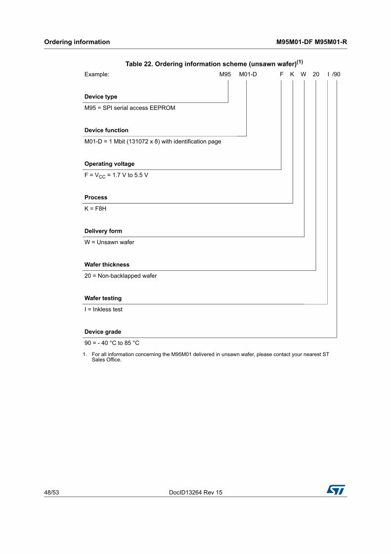
Table 22. Ordering information scheme (unsawn wafer)(1)
1. For all information concerning the M95M01 delivered in unsawn wafer, please contact your nearest ST Sales Office.
Example: M95 M01-D F K W 20 I /90
Device type
M95 = SPI serial access EEPROM
Device function
M01-D = 1 Mbit (131072 x 8) with identification page
Operating voltage
F = VCC = 1.7 V to 5.5 V
Process
K = F8H
Delivery form
W = Unsawn wafer
Wafer thickness
20 = Non-backlapped wafer
Wafer testing
I = Inkless test
Device grade
90 = - 40 °C to 85 °C

DocID13264 Rev 15 49/53
M95M01-DF M95M01-R Ordering information
52
Note: Parts marked as “ES”, “E” or accompanied by an Engineering Sample notification letter, are not yet qualified and therefore not approved for use in production. ST is not responsible for any consequences resulting from such use. In no event will ST be liable for the customer using any of these engineering samples in production. ST Quality has to be contacted prior to any decision to use these Engineering samples to run qualification activity.
Revision history M95M01-DF M95M01-R
50/53 DocID13264 Rev 15
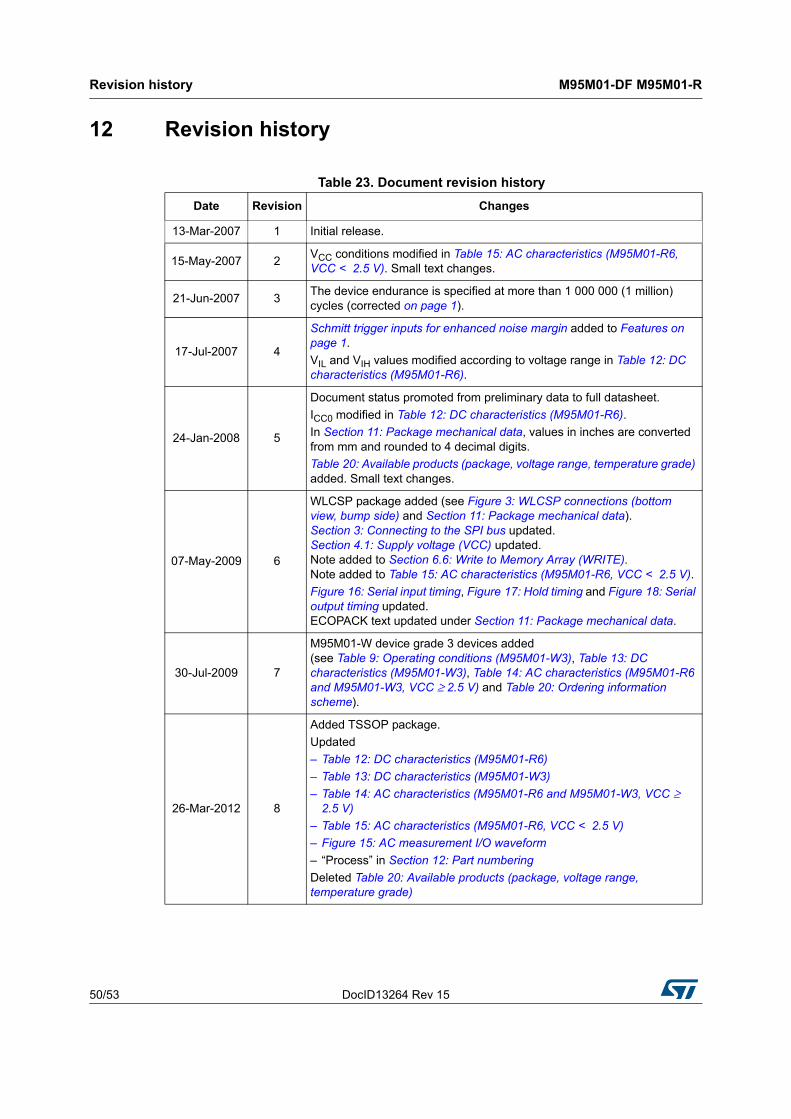
12 Revision history
Table 23. Document revision history
Date Revision Changes
13-Mar-2007 1 Initial release.
15-May-2007 2VCC conditions modified in Table 15: AC characteristics (M95M01-R6, VCC < 2.5 V). Small text changes.
21-Jun-2007 3The device endurance is specified at more than 1 000 000 (1 million) cycles (corrected on page 1).
17-Jul-2007 4
Schmitt trigger inputs for enhanced noise margin added to Features on page 1.
VIL and VIH values modified according to voltage range in Table 12: DC characteristics (M95M01-R6).
24-Jan-2008 5
Document status promoted from preliminary data to full datasheet.
ICC0 modified in Table 12: DC characteristics (M95M01-R6).
In Section 11: Package mechanical data, values in inches are converted from mm and rounded to 4 decimal digits.
Table 20: Available products (package, voltage range, temperature grade) added. Small text changes.
07-May-2009 6
WLCSP package added (see Figure 3: WLCSP connections (bottom view, bump side) and Section 11: Package mechanical data). Section 3: Connecting to the SPI bus updated. Section 4.1: Supply voltage (VCC) updated. Note added to Section 6.6: Write to Memory Array (WRITE). Note added to Table 15: AC characteristics (M95M01-R6, VCC < 2.5 V).
Figure 16: Serial input timing, Figure 17: Hold timing and Figure 18: Serial output timing updated. ECOPACK text updated under Section 11: Package mechanical data.
30-Jul-2009 7
M95M01-W device grade 3 devices added (see Table 9: Operating conditions (M95M01-W3), Table 13: DC characteristics (M95M01-W3), Table 14: AC characteristics (M95M01-R6 and M95M01-W3, VCC ≥ 2.5 V) and Table 20: Ordering information scheme).
26-Mar-2012 8
Added TSSOP package.
Updated
– Table 12: DC characteristics (M95M01-R6)
– Table 13: DC characteristics (M95M01-W3)
– Table 14: AC characteristics (M95M01-R6 and M95M01-W3, VCC ≥ 2.5 V)
– Table 15: AC characteristics (M95M01-R6, VCC < 2.5 V)
– Figure 15: AC measurement I/O waveform
– “Process” in Section 12: Part numbering
Deleted Table 20: Available products (package, voltage range, temperature grade)

DocID13264 Rev 15 51/53
M95M01-DF M95M01-R Revision history
52
20-Jun-2012 9
Datasheet split into:
– M95M01-125 datasheet for automotive products (range 3),
– M95M01-DF, M95M01-R (this datasheet) for standard products (range 6).
Updated:
– WLCSP package dimensions: Figure 44: M95080-DFCS6TP/K, WLCSP 8-bump wafer-level chip scale package outline and Table 60: M95080-DFCS6TP/K, WLCSP 8-bump wafer-level chip scale package mechanical data
– Cycling and data retention performances (4 million Write cycles, 200-year data retention)
– Table 14: DC characteristics updated with 1.7 V values
– Table 15: AC characteristics updated with 16 MHz clock
Added:
– Identification page (M95M01-DF)
– 1.7 V/5.5 V device (reference M95M01-DF)
Deleted reference M95M01-W3
06-Jul-2012 10 Updated WLCSP package reference from “CT” to “CS”.
3-Sep-2012 11Fixed some errors in Figure 3: WLCSP connections for M95M01-DFCS6TP/K and M95M01-DFCU6TP/K (top view, marking side, with bumps on the underside)
25-May-2015 12
Replaced “ball” by “bump” in the entire document.
Updated Features and WLCSP package figure on cover page.
Removed Caution note on UV exposure in Section 1: Description.
Updated Figure 3: WLCSP connections for M95M01-DFCS6TP/K and M95M01-DFCU6TP/K (top view, marking side, with bumps on the underside), Figure 4: Block diagram and Figure 14: Page Write (WRITE) sequence.
Updated Section 5.1.3: Power-up conditions, Section 5.3: Hold condition, Section 6: Instructions. and Section 7.2: Initial delivery state.
Updated Table 7: Absolute maximum ratings and its footnotes.
Updated Section 10: Package information with changes in each of Sections 10.1: SO8N package information, 10.2: TSSOP8 package information and 10.8: WLCSP package information.
Updated Table 31: Ordering information scheme and added Note: on Engineering samples.
Updated Disclaimer.
30-Jun-2016 13
Updated Figure 8: Write Enable (WREN) sequence and Figure 9: Write Disable (WRDI) sequence.
Updated footnote 1 of Table 7: Absolute maximum ratings.
Updated caption of Figure 25: TSSOP8 – 8-lead thin shrink small outline, 3 x 4.4 mm, 0.65 mm pitch, package outline and of Table 17: TSSOP8 – 8-lead thin shrink small outline, 3 x 4.4 mm, 0.65 mm pitch, package mechanical data.
Updated Section 10.8: WLCSP package information.
Updated Table 31: Ordering information scheme.
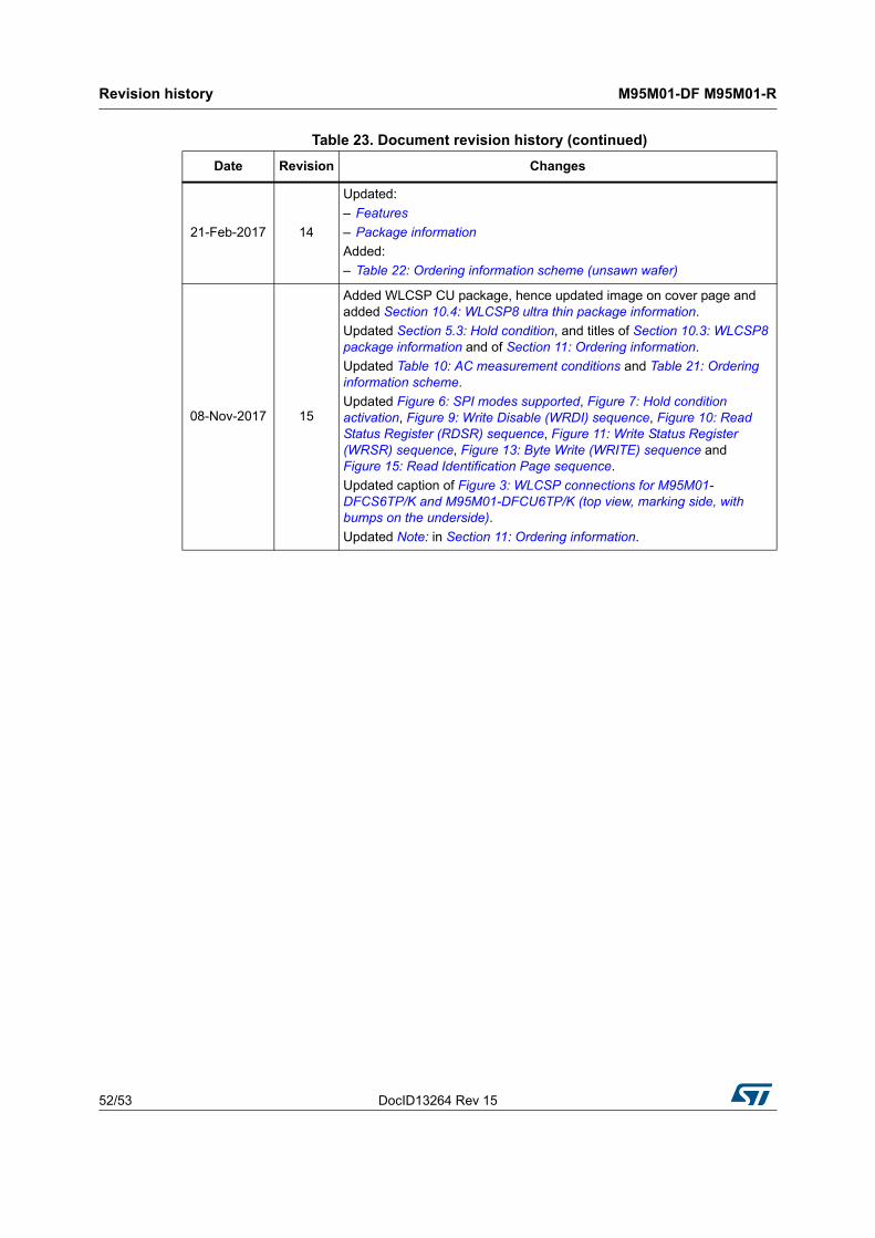
Table 23. Document revision history (continued)
Date Revision Changes
Revision history M95M01-DF M95M01-R
52/53 DocID13264 Rev 15
21-Feb-2017 14
Updated:
– Features
– Package information
Added:
– Table 22: Ordering information scheme (unsawn wafer)
08-Nov-2017 15
Added WLCSP CU package, hence updated image on cover page and added Section 10.4: WLCSP8 ultra thin package information.
Updated Section 5.3: Hold condition, and titles of Section 10.3: WLCSP8 package information and of Section 11: Ordering information.
Updated Table 10: AC measurement conditions and Table 21: Ordering information scheme.
Updated Figure 6: SPI modes supported, Figure 7: Hold condition activation, Figure 9: Write Disable (WRDI) sequence, Figure 10: Read Status Register (RDSR) sequence, Figure 11: Write Status Register (WRSR) sequence, Figure 13: Byte Write (WRITE) sequence and Figure 15: Read Identification Page sequence.
Updated caption of Figure 3: WLCSP connections for M95M01-DFCS6TP/K and M95M01-DFCU6TP/K (top view, marking side, with bumps on the underside).
Updated Note: in Section 11: Ordering information.
Table 23. Document revision history (continued)
Date Revision Changes

DocID13264 Rev 15 53/53
M95M01-DF M95M01-R
53
IMPORTANT NOTICE – PLEASE READ CAREFULLY
STMicroelectronics NV and its subsidiaries (“ST”) reserve the right to make changes, corrections, enhancements, modifications, and improvements to ST products and/or to this document at any time without notice. Purchasers should obtain the latest relevant information on ST products before placing orders. ST products are sold pursuant to ST’s terms and conditions of sale in place at the time of order acknowledgement.
Purchasers are solely responsible for the choice, selection, and use of ST products and ST assumes no liability for application assistance or the design of Purchasers’ products.
No license, express or implied, to any intellectual property right is granted by ST herein.
Resale of ST products with provisions different from the information set forth herein shall void any warranty granted by ST for such product.
ST and the ST logo are trademarks of ST. All other product or service names are the property of their respective owners.
Information in this document supersedes and replaces information previously supplied in any prior versions of this document.
© 2017 STMicroelectronics – All rights reserved