Embed Size (px)
Citation preview
1
High-Voltage High Slew-Rate Op-Amp Design
Team Tucson:
Erik Mentze
Jenny Phillips
Project Sponsor:
Apex Microtechnology
Project Advisors:
Dave Cox
Herb Hess
2
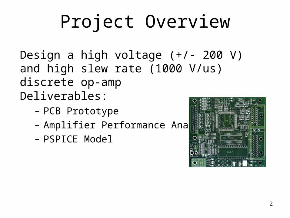
Project Overview
Deliverables: – PCB Prototype– Amplifier Performance Analysis– PSPICE Model
Design a high voltage (+/- 200 V) and high slew rate (1000 V/us) discrete op-amp

3
Specific Design Challenges
• Power Limitation (P=IV)• High Voltage required
• Slew Rate = I/Cc
Power Limitation
Device Voltage Limitations Device Current Limitations
Slew Rate LimitationsOutput Voltage Limitations
4
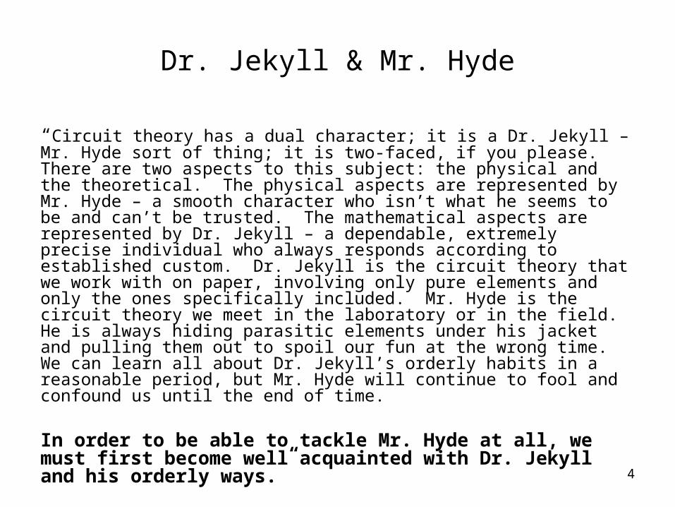
Dr. Jekyll & Mr. Hyde
“Circuit theory has a dual character; it is a Dr. Jekyll – Mr. Hyde sort of thing; it is two-faced, if you please. There are two aspects to this subject: the physical and the theoretical. The physical aspects are represented by Mr. Hyde – a smooth character who isn’t what he seems to be and can’t be trusted. The mathematical aspects are represented by Dr. Jekyll – a dependable, extremely precise individual who always responds according to established custom. Dr. Jekyll is the circuit theory that we work with on paper, involving only pure elements and only the ones specifically included. Mr. Hyde is the circuit theory we meet in the laboratory or in the field. He is always hiding parasitic elements under his jacket and pulling them out to spoil our fun at the wrong time. We can learn all about Dr. Jekyll’s orderly habits in a reasonable period, but Mr. Hyde will continue to fool and confound us until the end of time.
In order to be able to tackle Mr. Hyde at all, we must first become well acquainted with Dr. Jekyll and his orderly ways.”
-Ernst A. Guillemin Taken from the preface to his 1953 book Introductory Circuit Theory.

5
Project Breakdown
– Dr. Jekyll – General Amplifier Topologies• Find topology candidates• Throw out those that are obviously deficient• Analytically compare the “finalists” to make the
best choice
– Mr. Hyde – Hardware Implementation• Find components that meet our design
requirements• Adapt chosen topology to meet physical
requirements• Simulate Implementation, comparing to Dr.
Jekyll’s analytic models• Implement design, comparing results to simulation
and analytic models
6
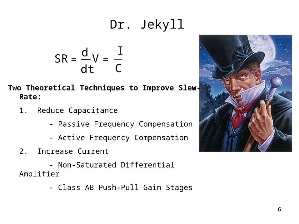
Dr. Jekyll
Two Theoretical Techniques to Improve Slew-Rate:
1. Reduce Capacitance
- Passive Frequency Compensation
- Active Frequency Compensation
2. Increase Current
- Non-Saturated Differential Amplifier
- Class AB Push-Pull Gain Stages
SRtVd
d
I
C
7
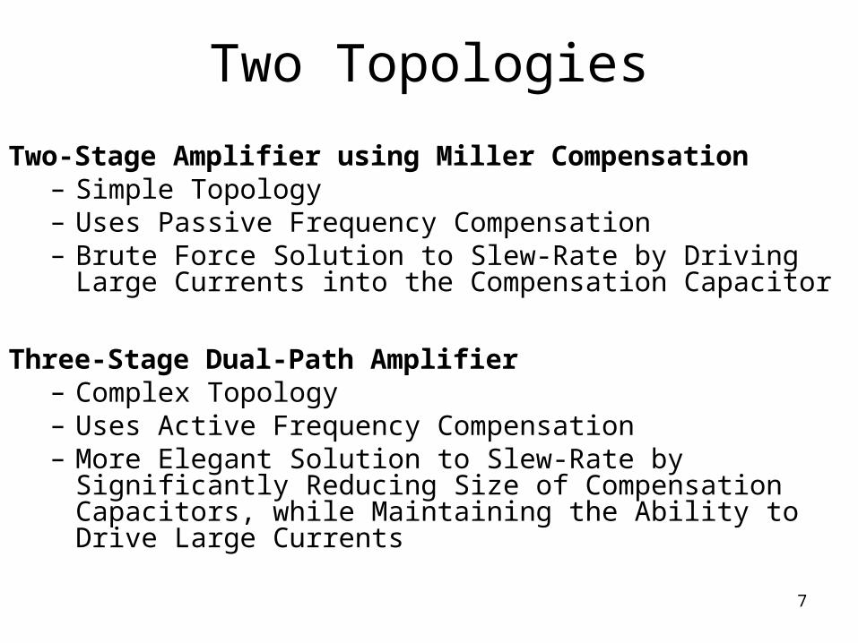
Two Topologies
Two-Stage Amplifier using Miller Compensation– Simple Topology– Uses Passive Frequency Compensation– Brute Force Solution to Slew-Rate by Driving Large Currents
into the Compensation Capacitor
Three-Stage Dual-Path Amplifier– Complex Topology– Uses Active Frequency Compensation– More Elegant Solution to Slew-Rate by Significantly
Reducing Size of Compensation Capacitors, while Maintaining the Ability to Drive Large Currents
8
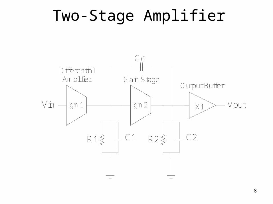
Two-Stage Amplifier
Cc
gm1 gm2 X1 VoutVin
C1R1 C2R2
DifferentialAmplifier Gain Stage
Output Buffer
9
Two-Stage Amplifier
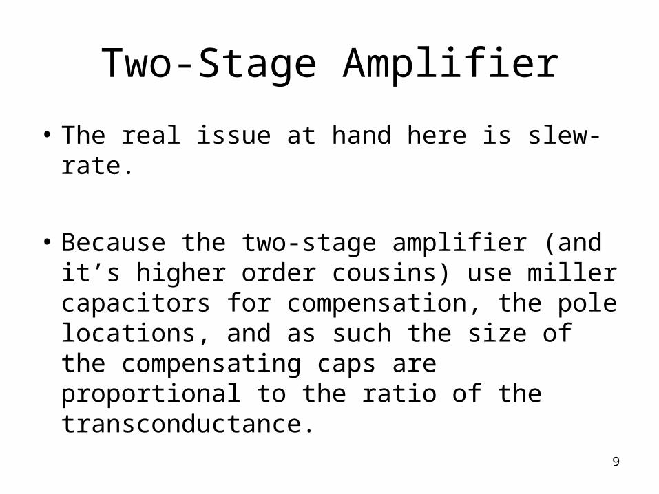
• The real issue at hand here is slew-rate.
• Because the two-stage amplifier (and it’s higher order cousins) use miller capacitors for compensation, the pole locations, and as such the size of the compensating caps are proportional to the ratio of the transconductance.
10
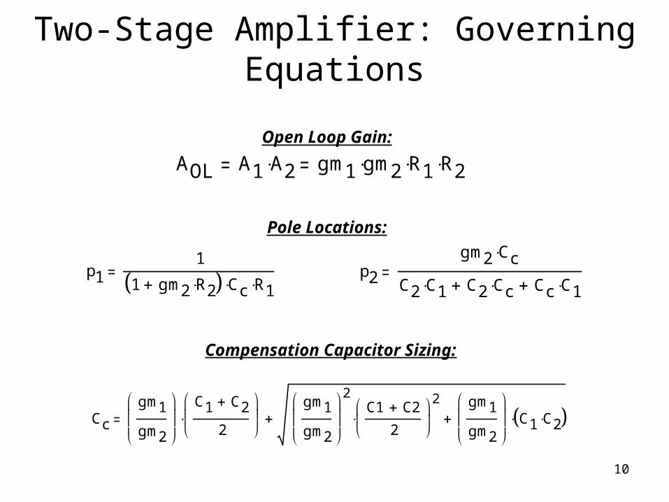
Two-Stage Amplifier: Governing Equations
p11
1 gm2 R2 Cc R1p2
gm2 Cc
C2 C1 C2 Cc Cc C1
Cc
gm1
gm2
C1 C2
2
gm1
gm2
2C1 C2
2
2
gm1
gm2
C1 C2
AOL A1 A2 gm1 gm2 R1 R2Open Loop Gain:
Pole Locations:
Compensation Capacitor Sizing:
11
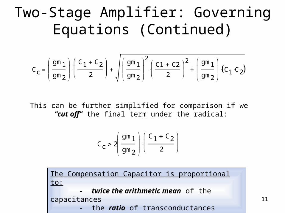
Two-Stage Amplifier: Governing Equations (Continued)
This can be further simplified for comparison if we “cut off” the final term under the radical:
The Compensation Capacitor is proportional to:- twice the arithmetic mean of the capacitances- the ratio of transconductances
Cc 2gm1
gm2
C1 C2
2
Cc
gm1
gm2
C1 C2
2
gm1
gm2
2C1 C2
2
2
gm1
gm2
C1 C2
12
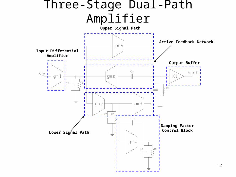
Three-Stage Dual-Path Amplifier
gm1
gm2
gma
gm4
gm5
X1
gm3
C1
Ca
Cb
R1
C2 R2
C4 R4
CL RL
VoutVin
Input DifferentialAmplifier
Upper Signal Path
Lower Signal Path
Damping-FactorControl Block
Active Feedback Network
Output Buffer
13
Three-Stage Dual-Path Amplifier
• Uses two Active Compensation techniques:– Damping-Factor Control block
• Removes a compensation capacitor from the output• Replaces it with an Active-C block that uses a significantly
smaller capacitor.• Introduces a high degree of controllability of the non-
dominate poles.
– Active-Capacitive-Feedback network• Adds a positive gain stage in series with the dominate
compensation capacitor, reducing the required cap size.• Gives an enormous amount of flexibility in determining the
amplifier’s dominate poles.
14
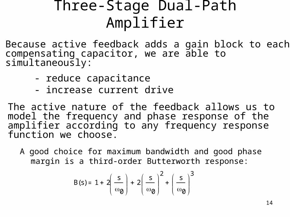
Three-Stage Dual-Path Amplifier
Because active feedback adds a gain block to each compensating capacitor, we are able to simultaneously:
- reduce capacitance- increase current drive
The active nature of the feedback allows us to model the frequency and phase response of the amplifier according to any frequency response function we choose.
A good choice for maximum bandwidth and good phase margin is a third-order Butterworth response:
B s( ) 1 2s
0
2s
0
2
s
0
3
15
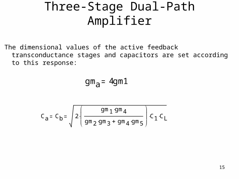
Three-Stage Dual-Path Amplifier
The dimensional values of the active feedback transconductance stages and capacitors are set according to this response:
Ca Cb 2gm1 gm4
gm2 gm3 gm4 gm5
C1 CL
gma 4gm1
16
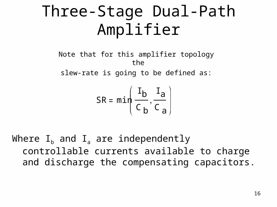
Three-Stage Dual-Path Amplifier
Note that for this amplifier topology the
slew-rate is going to be defined as:
SR minI b
C b
I a
C a
Where Ib and Ia are independently controllable currents available to charge and discharge the compensating capacitors.
17
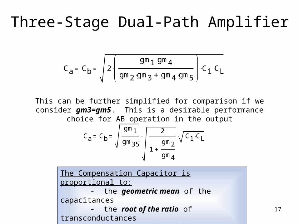
Three-Stage Dual-Path Amplifier
Ca Cb 2gm1 gm4
gm2 gm3 gm4 gm5
C1 CL
This can be further simplified for comparison if we consider gm3=gm5. This is a desirable performance choice for AB operation in the output
Ca Cb
gm1
gm35
2
1gm2
gm4
C1 CL
The Compensation Capacitor is proportional to:- the geometric mean of the capacitances- the root of the ratio of transconductances- a constant that is less than one
18
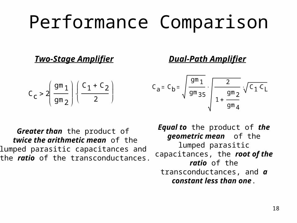
Performance Comparison
Two-Stage Amplifier Dual-Path Amplifier
Cc 2gm1
gm2
C1 C2
2
Ca Cb
gm1
gm35
2
1gm2
gm4
C1 CL
Greater than the product of twice the arithmetic mean of the
lumped parasitic capacitances and the ratio of the transconductances.
Equal to the product of the geometric mean of the lumped
parasitic capacitances, the root of the ratio of the transconductances,
and a constant less than one.
19
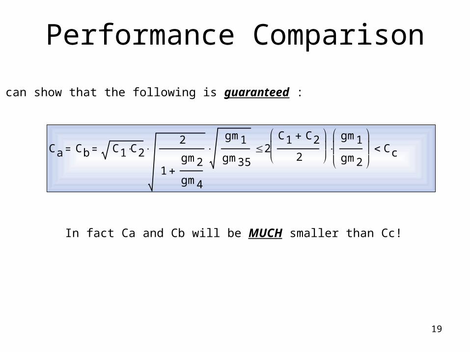
Performance Comparison
We can show that the following is guaranteed :
Ca Cb C1 C22
1gm2
gm4
gm1
gm35 2
C1 C2
2
gm1
gm2
Cc
In fact Ca and Cb will be MUCH smaller than Cc!
20
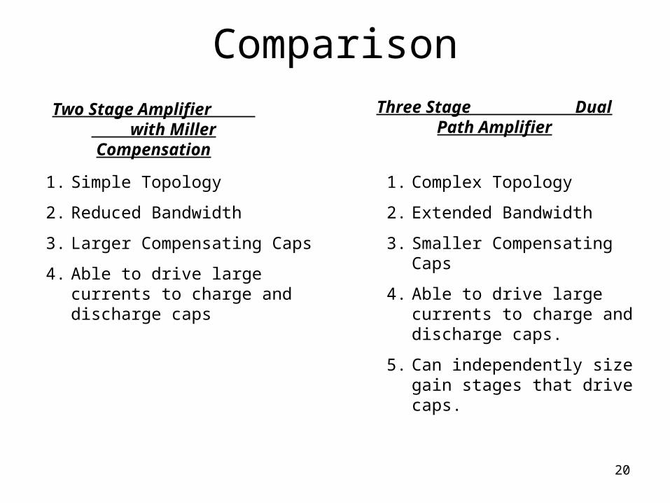
ComparisonTwo Stage Amplifier
with Miller Compensation
Three Stage Dual Path Amplifier
1. Simple Topology
2. Reduced Bandwidth
3. Larger Compensating Caps
4. Able to drive large currents to charge and discharge caps
1. Complex Topology
2. Extended Bandwidth
3. Smaller Compensating Caps
4. Able to drive large currents to charge and discharge caps.
5. Can independently size gain stages that drive caps.

21
Specific Gain Stages
22
Differential Amplifier
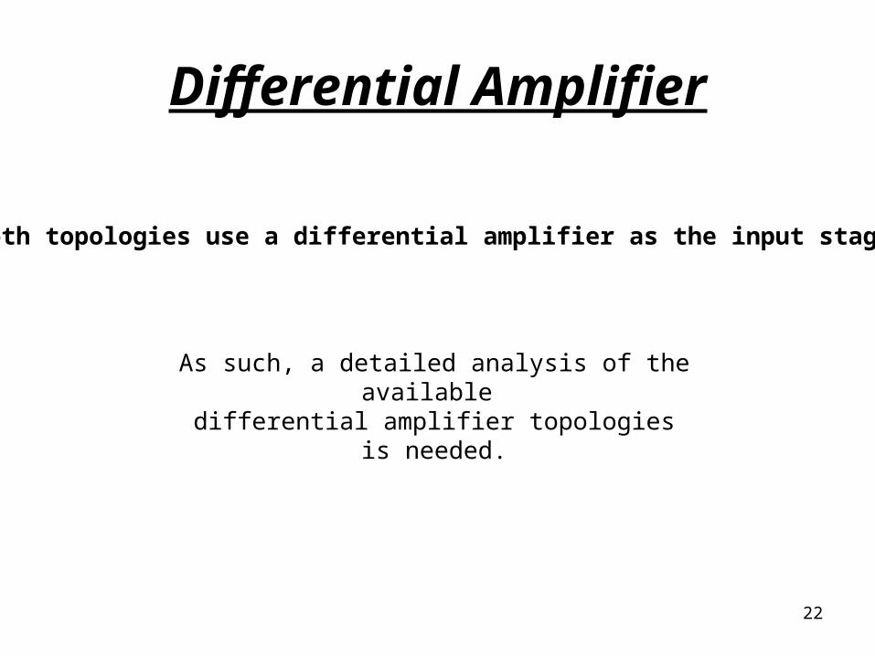
Both topologies use a differential amplifier as the input stage.
As such, a detailed analysis of the available differential amplifier topologies is needed.
23
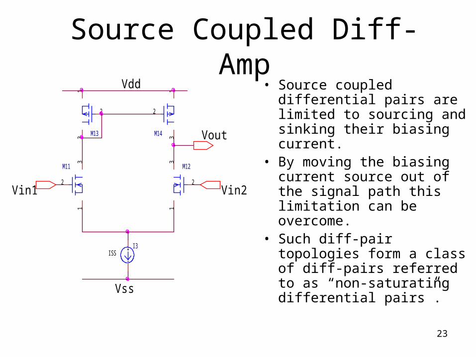
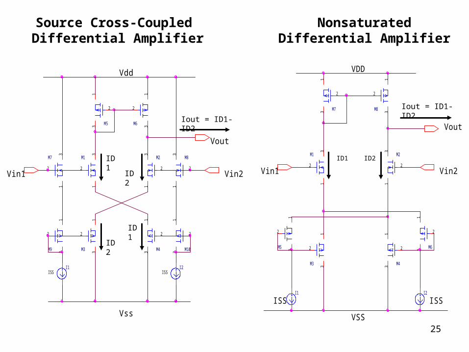
• Source coupled differential pairs are limited to sourcing and sinking their biasing current.
• By moving the biasing current source out of the signal path this limitation can be overcome.
• Such diff-pair topologies form a class of diff-pairs referred to as “non-saturating differential pairs”.
1
2
3
M111
2
3M12
1
2
3
M13
1
2
3
M14
I3ISS
Vout
Vin2Vin1
Vss
Vdd
Source Coupled Diff-Amp
24
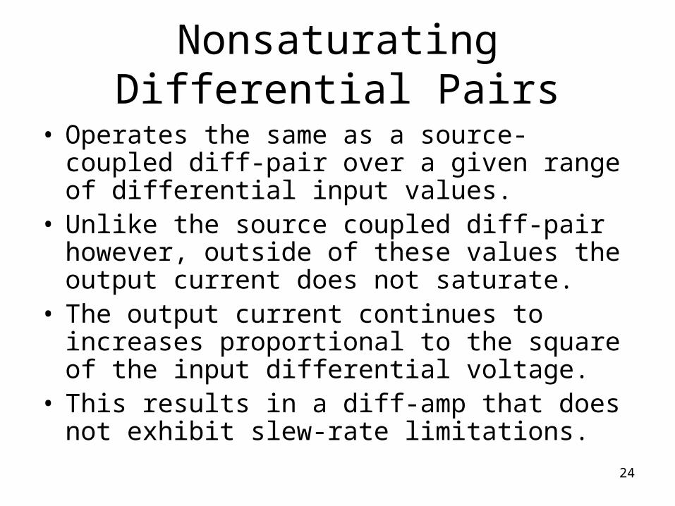
Nonsaturating Differential Pairs
• Operates the same as a source-coupled diff-pair over a given range of differential input values.
• Unlike the source coupled diff-pair however, outside of these values the output current does not saturate.
• The output current continues to increases proportional to the square of the input differential voltage.
• This results in a diff-amp that does not exhibit slew-rate limitations.
25
1
2
3
M1
1
2
3
M2
1
2
3
M3
1
2
3
M4
1
2
3
M5
1
2
3
M6
1
2
3
M7
12
3
M8
1
2
3
M9
1
2
3
M10
I1ISS
I2ISS
Vout
Vin2Vin1
Vss
Vdd
ID1
ID2
Iout = ID1-ID2
ID1
ID2
1
2
3
M1
1
2
3
M2
1
2
3
M3
1
2
3
M4
1
2
3
M5
1
2
3
M6
1
2
3
M7
1
2
3
M8
I1
ISSI2
ISS
Vin2Vin1
Vout
VDD
VSS
ID1 ID2
Iout = ID1-ID2
Source Cross-Coupled Differential Amplifier
NonsaturatedDifferential Amplifier
26
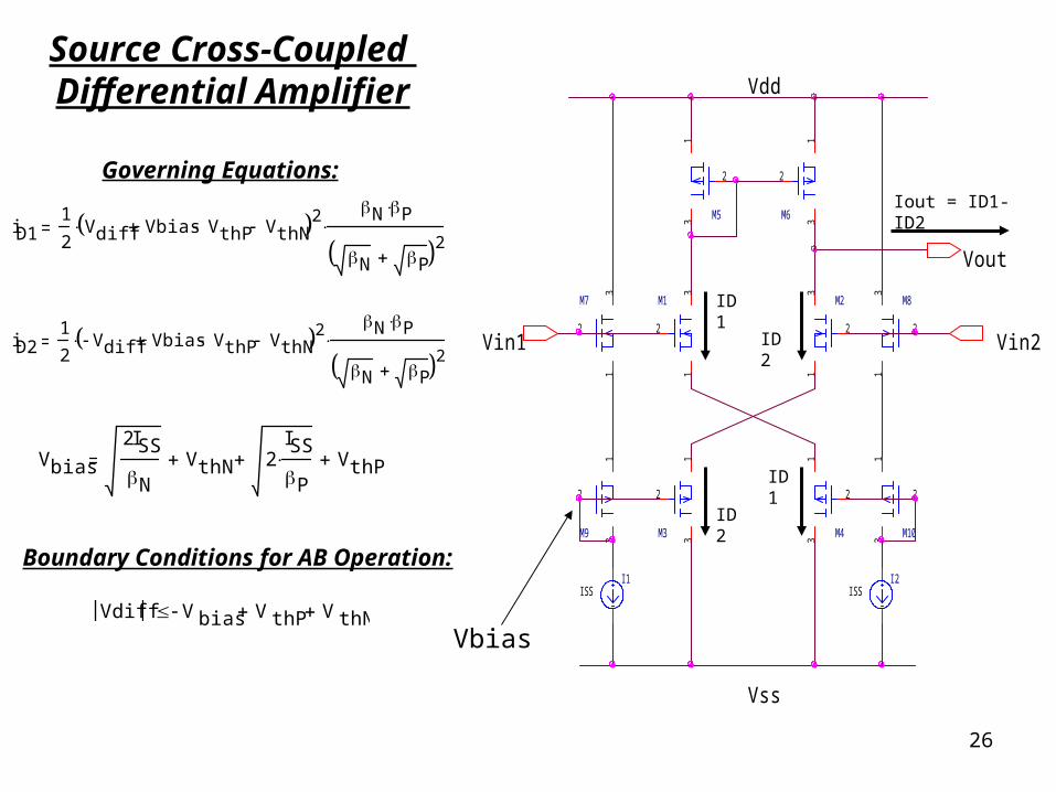
Source Cross-Coupled Differential Amplifier
1
2
3
M1
1
2
3
M2
1
2
3
M3
1
2
3
M4
1
2
3
M5
1
2
3
M6
1
2
3
M7
1
2
3
M8
1
2
3
M9
1
2
3
M10
I1ISS
I2ISS
Vout
Vin2Vin1
Vss
Vdd
ID1
ID2
Iout = ID1-ID2
ID1
ID2
iD11
2Vdiff Vbias VthP VthN 2
N P
N P 2
iD21
2Vdiff Vbias VthP VthN 2
N P
N P 2
Governing Equations:
Boundary Conditions for AB Operation:
Vdiff Vbias VthP VthNVbias
Vbias
2ISS
NVthN 2
ISS
P VthP
27
1
2
3
M1
1
2
3
M2
1
2
3
M3
1
2
3
M4
1
2
3M5
1
2
3
M6
1
2
3
M7
1
2
3
M8
I1
ISSI2
ISS
Vin2Vin1
Vout
VDD
VSS
ID1 ID2
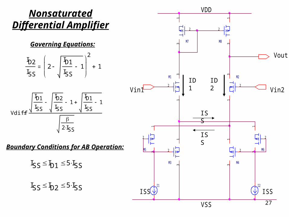
NonsaturatedDifferential Amplifier
Governing Equations:
Boundary Conditions for AB Operation:
ISS
ISS
ID2
ISS2
ID1
ISS1
2
1
ISS ID1 5 ISS
ISS ID2 5 ISS
Vdiff
ID1
ISS
ID2
ISS 1
ID1
ISS1
2 ISS
28
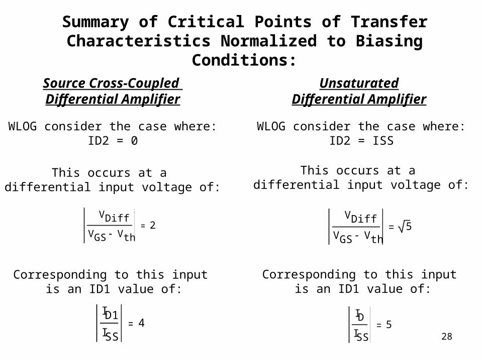
Summary of Critical Points of Transfer Characteristics Normalized to Biasing Conditions:
VDiff
VGS Vth2
ID1
ISS4
VDiff
VGS Vth5
ID
ISS5
Source Cross-Coupled Differential Amplifier
UnsaturatedDifferential Amplifier
WLOG consider the case where:ID2 = 0
WLOG consider the case where:ID2 = ISS
This occurs at a differential input voltage of:
Corresponding to this input is an ID1 value of:
This occurs at a differential input voltage of:
Corresponding to this input is an ID1 value of:
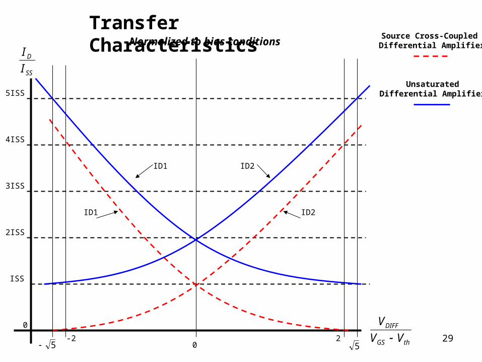
29
ISS
2ISS
3ISS
4ISS
5ISS
0
0-2 2
ID1 ID2
ID1 ID2
thGS
DIFF
VV
V
55
SS
D
I
I
Source Cross-Coupled Differential Amplifier
UnsaturatedDifferential Amplifier
Transfer CharacteristicsNormalized to bias conditions
30
5thGS
DIFF
VV
V
SS
out
I
I
-2
2
4ISS
- 4ISS
- 3ISS
- 2ISS
- ISS
3ISS
2ISS
ISS5
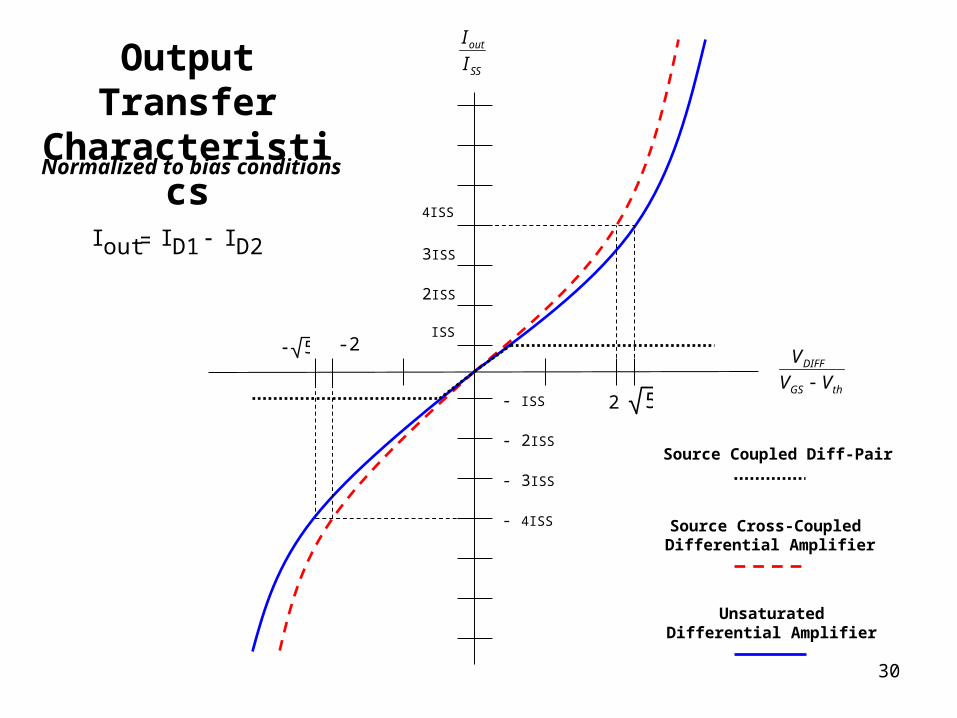
Source Cross-Coupled Differential Amplifier
UnsaturatedDifferential Amplifier
Source Coupled Diff-Pair
Output Transfer Characteristics
I out I D1 I D2
Normalized to bias conditions
31
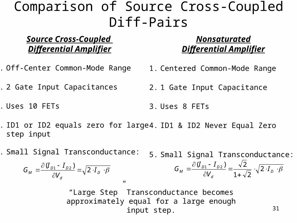
1. Off-Center Common-Mode Range
2. 2 Gate Input Capacitances
3. Uses 10 FETs
4. ID1 or ID2 equals zero for largestep input
5. Small Signal Transconductance:
D
d
DDM I
V
IIG 2
)( 21
Comparison of Source Cross-Coupled Diff-Pairs
Source Cross-Coupled Differential Amplifier
NonsaturatedDifferential Amplifier
1. Centered Common-Mode Range
2. 1 Gate Input Capacitance
3. Uses 8 FETs
4. ID1 & ID2 Never Equal Zero
5. Small Signal Transconductance:
D
d
DDM I
V
IIG 2
21
2)( 21
“Large Step” Transconductance becomes approximately equal for a large enough input step.

32
THE BIG QUESTION!THE BIG QUESTION!

33
Which one has the most Which one has the most useful advantages???useful advantages???
34
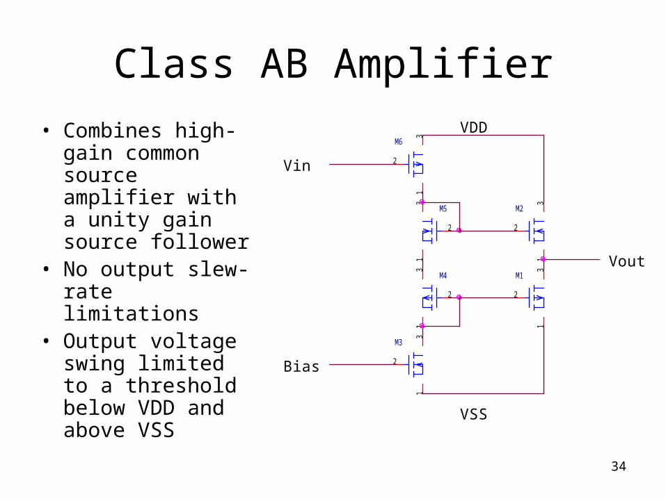
Class AB Amplifier
• Combines high-gain common source amplifier with a unity gain source follower
• No output slew-rate limitations
• Output voltage swing limited to a threshold below VDD and above VSS
1
2
3
M6
1
2
3
M1
1
2
3
M4
1
2
3
M2
1
2
3
M3
1
2
3
M5
VDD
Vin
Bias
Vout
VSS
35
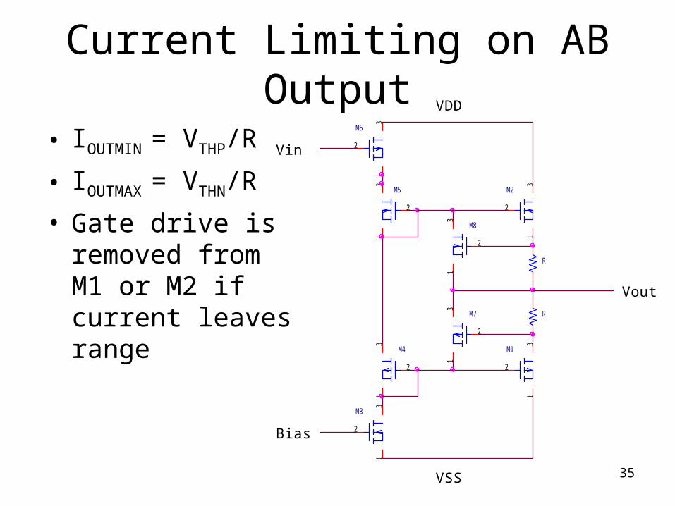
Current Limiting on AB Output
• IOUTMIN = VTHP/R
• IOUTMAX = VTHN/R
• Gate drive is removed from M1 or M2 if current leaves range
1
2
3
M2
1
2
3
M8
1
2
3
M1
1
2
3
M7
R
R
1
2
3
M5
1
2
3
M3
1
2
3
M4
1
2
3
M6
Vout
VDD
Vin
Bias
VSS
36
Mr. Hyde
37
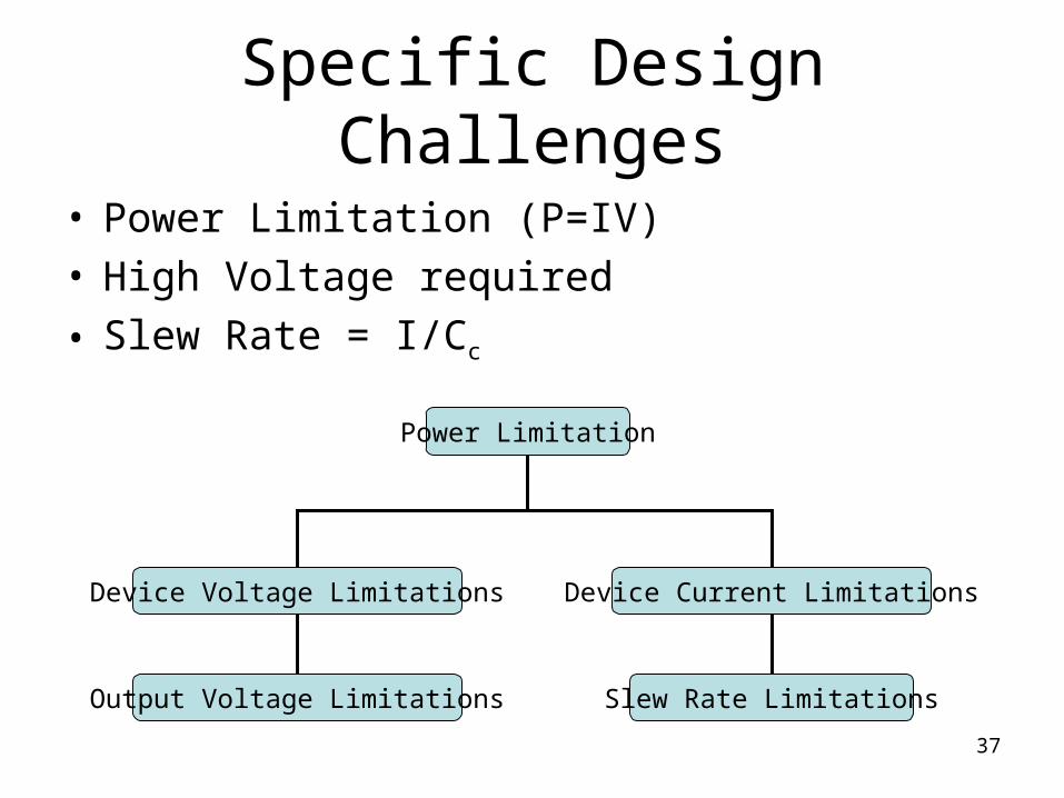
Specific Design Challenges
• Power Limitation (P=IV)• High Voltage required
• Slew Rate = I/Cc
Power Limitation
Device Voltage Limitations Device Current Limitations
Slew Rate LimitationsOutput Voltage Limitations
38
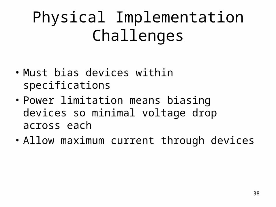
Physical Implementation Challenges
• Must bias devices within specifications
• Power limitation means biasing devices so minimal voltage drop across each
• Allow maximum current through devices
39
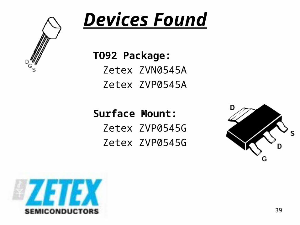
Devices Found
TO92 Package:
Zetex ZVN0545A
Zetex ZVP0545A
Surface Mount:
Zetex ZVP0545G
Zetex ZVP0545G
40
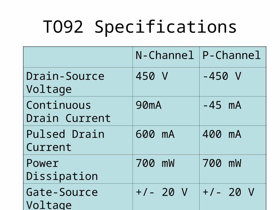
TO92 Specifications
N-Channel P-Channel
Drain-Source Voltage
450 V -450 V
Continuous Drain Current
90mA -45 mA
Pulsed Drain Current 600 mA 400 mA
Power Dissipation 700 mW 700 mW
Gate-Source Voltage +/- 20 V +/- 20 V
41
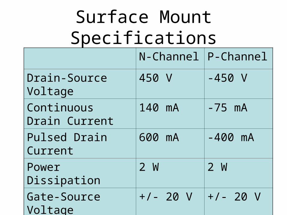
Surface Mount Specifications
N-Channel P-Channel
Drain-Source Voltage
450 V -450 V
Continuous Drain Current
140 mA -75 mA
Pulsed Drain Current 600 mA -400 mA
Power Dissipation 2 W 2 W
Gate-Source Voltage +/- 20 V +/- 20 V
42
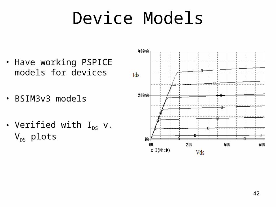
Device Models
• Have working PSPICE models for devices
• BSIM3v3 models
• Verified with IDS v. VDS plots
43
Cost of Devices
• NMOS (TO92)– 10 Parts for $20.70– 100 Parts for $124.20– 500 Parts for $483.00
• PMOS (TO92)– 10 Parts for $23.22– 100 Parts for $139.32– 500 Parts for $541.80
• NMOS (Surface Mount)– 10 Parts for $11.25– 100 Parts for $67.50– 500 Parts for $262.50
• PMOS (Surface Mount)– 10 Parts for $13.55– 100 Parts for $81.27– 500 Parts for $316.05
44
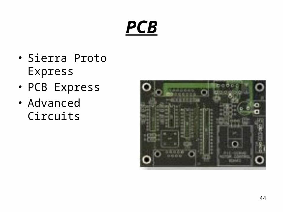
PCB
• Sierra Proto Express• PCB Express• Advanced Circuits
45
Project Schedule
• Finalize Amplifier Topology – 11/19/04• Preliminary Simulation Results – 1/17/05• Final Simulation Results – 1/28/05• Perfboard Testing Completed – 2/11/05• PCB Layout Finalized – 2/18/05• Preliminary Modeling – 3/4/05• Write Test Procedures – 3/11/05• PCB Test and Measurement – 3/19/05• Final Modeling – 3/25/05• Tie up Loose Ends by EXPO! – 4/29/05
46
Q & AQ & A
47
References[1] H. Lee, et al., “A Dual-Path Bandwidth Extension Amplifier Topology With Dual-Loop Parallel Compensation,” IEEE
J. Solid-State Circuits, vol. 38, no. 10, Oct. 2003.
[2] H.T. Ng, et al., “A Multistage Amplifier Technique with Embedded Frequency Compensation,” IEEE J. Solid-State Circuits, vol. 34, no 3, March 1999.
[3] H. Lee, et al., “Active-Feedback Frequency-Compensation Technique for Low-Power Multistage Amplifiers,” IEEE J. Solid-State Circuits, vol. 38, no 3, March 2003.
[4] K. Leung, et al., “Three-Stage Large Capacitive Load Amplifier with Damping-Factor-Control Frequency Compensation,” IEEE Transactions on Solid-State Circuits, vol. 35, no 2, February 2000.
[5] H. Lee, et al., “Advances in Active-Feedback Frequency Compensation with Power Optimization and Transient Improvement,” IEEE Transactions on Circuits and Systems, vol. 51, no 9, September 2004.
[6] B. Lee, et al., “A High Slew-Rate CMOS Amplifier for Analog Signal Processing,” IEEE J. Solid-State Circuits, vol. 25, no. 3, June 1990.
[7] E. Seevinck, et al., “A Versatile CMOS Linear Transconductor/Square-Law Function Circuit,” IEEE J. Solid-State Circuits, vol. SC-22, no. 3, June 1987.
[8] J. Baker, et al., CMOS: Circuit Design, Layout, and Simulation. New York, NY: John Wiley & Sons, Inc., 1998.
[9] B. Razavi, Design of Analog CMOS Integrated Circuits. Boston, MA: McGraw Hill, 2001.
[10] Sedra, Smith, Microelectronic Circuits, 5th ed. New York, NY: Oxford University Press, 2004.
[11] Schaumann, Van Valkenburg, Design of Analog Filters. New York, NY: Oxford University Press, 2001.
[12] V. Kosmala, Real Analysis: Single and Multivariable. Upper Saddle River, NJ: Prentice Hall, 2004.