Embed Size (px)
Citation preview
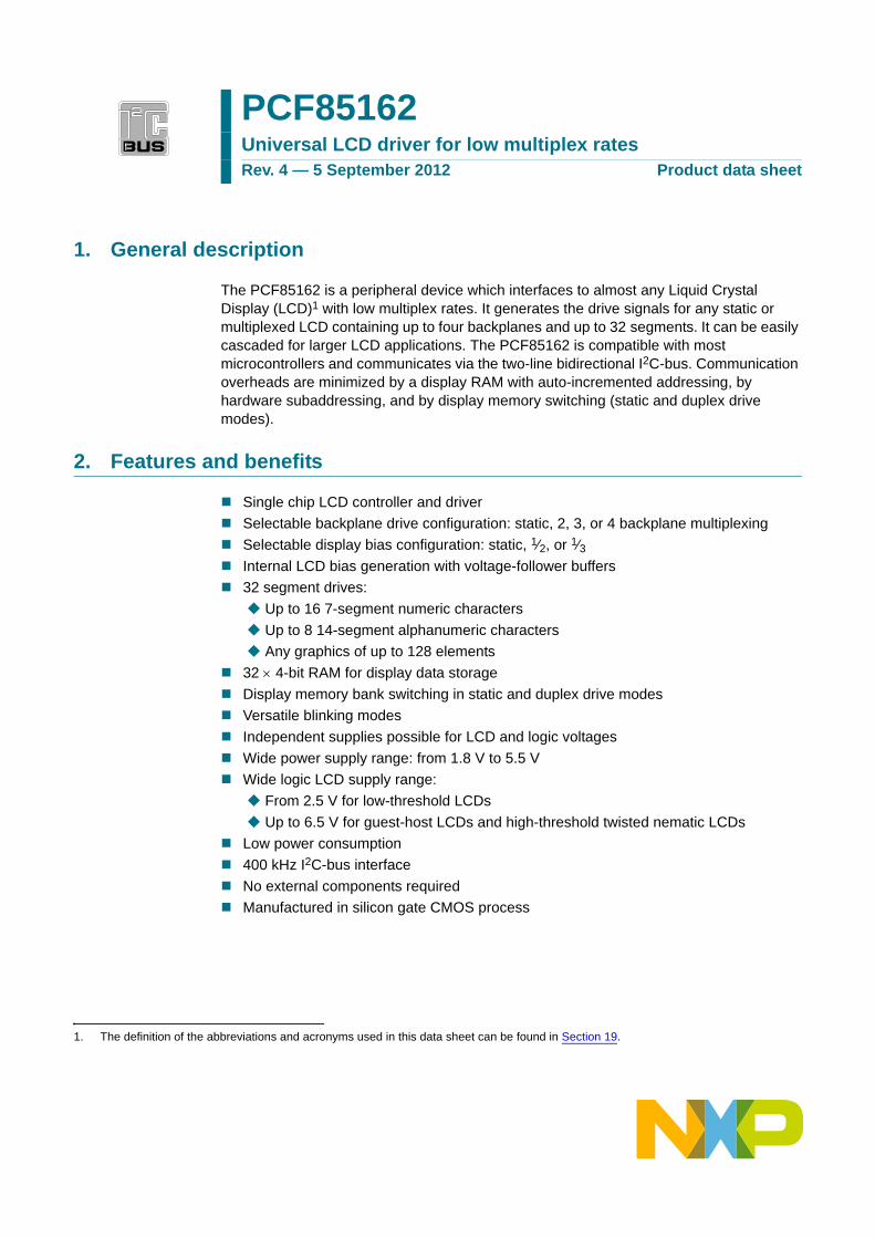
1. General description
The PCF85162 is a peripheral device which interfaces to almost any Liquid Crystal Display (LCD)1 with low multiplex rates. It generates the drive signals for any static or multiplexed LCD containing up to four backplanes and up to 32 segments. It can be easily cascaded for larger LCD applications. The PCF85162 is compatible with most microcontrollers and communicates via the two-line bidirectional I2C-bus. Communication overheads are minimized by a display RAM with auto-incremented addressing, by hardware subaddressing, and by display memory switching (static and duplex drive modes).
2. Features and benefits
Single chip LCD controller and driver
Selectable backplane drive configuration: static, 2, 3, or 4 backplane multiplexing
Selectable display bias configuration: static, 1⁄2, or 1⁄3 Internal LCD bias generation with voltage-follower buffers
32 segment drives:
Up to 16 7-segment numeric characters
Up to 8 14-segment alphanumeric characters
Any graphics of up to 128 elements
32 4-bit RAM for display data storage
Display memory bank switching in static and duplex drive modes
Versatile blinking modes
Independent supplies possible for LCD and logic voltages
Wide power supply range: from 1.8 V to 5.5 V
Wide logic LCD supply range:
From 2.5 V for low-threshold LCDs
Up to 6.5 V for guest-host LCDs and high-threshold twisted nematic LCDs
Low power consumption
400 kHz I2C-bus interface
No external components required
Manufactured in silicon gate CMOS process
PCF85162Universal LCD driver for low multiplex ratesRev. 4 — 5 September 2012 Product data sheet
1. The definition of the abbreviations and acronyms used in this data sheet can be found in Section 19.
PCF85162 All information provided in this document is subject to legal disclaimers. © NXP B.V. 2012. All rights reserved.
Product data sheet Rev. 4 — 5 September 2012 2 of 56
NXP Semiconductors PCF85162Universal LCD driver for low multiplex rates
3. Ordering information
3.1 Ordering options
4. Marking
Table 1. Ordering information
Type number Package
Name Description Version
PCF85162T TSSOP48 plastic thin shrink small outline package; 48 leads; body width 6.1 mm
SOT362-1
Table 2. Ordering options
Type number IC revision
Sales item (12NC) Delivery form
PCF85162T/1 1 935290708118 tape and reel, 13 inch
Table 3. Marking codes
Type number Marking code
PCF85162T/1 PCF85162T
PCF85162 All information provided in this document is subject to legal disclaimers. © NXP B.V. 2012. All rights reserved.
Product data sheet Rev. 4 — 5 September 2012 3 of 56
NXP Semiconductors PCF85162Universal LCD driver for low multiplex rates
5. Block diagram
Fig 1. Block diagram of PCF85162
013aaa064
CLK
SYNC
OSC
SCL
SA0
BP0
VDD
BP2 BP1 BP3
32
S0 to S31
A0 A1 A2
PCF85162 DISPLAYRAM
DISPLAY SEGMENT OUTPUTS
DISPLAY REGISTER
OUTPUT BANK SELECTAND BLINK CONTROL
DISPLAYCONTROLLER
BACKPLANEOUTPUTS
LCDVOLTAGE
SELECTOR
LCD BIASGENERATOR
CLOCK SELECTAND TIMING
BLINKERTIMEBASE
OSCILLATOR POWER-ONRESET
COMMANDDECODER
WRITE DATACONTROL
DATA POINTER ANDAUTO INCREMENT
INPUTFILTERS
I2C-BUSCONTROLLER
SUBADDRESSCOUNTERSDA
VSS
VLCD
PCF85162 All information provided in this document is subject to legal disclaimers. © NXP B.V. 2012. All rights reserved.
Product data sheet Rev. 4 — 5 September 2012 4 of 56
NXP Semiconductors PCF85162Universal LCD driver for low multiplex rates
6. Pinning information
6.1 Pinning
Top view. For mechanical details, see Figure 28.
Fig 2. Pin configuration for TSSOP48 (PCF85162T)
PCF85162T
S23 S22
S24 S21
S25 S20
S26 S19
S27 S18
S28 S17
S29 S16
S30 S15
S31 S14
SDA S13
SCL S12
SYNC S11
CLK S10
VDD S9
OSC S8
A0 S7
A1 S6
A2 S5
SA0 S4
VSS S3
VLCD S2
BP0 S1
BP2 S0
BP1 BP3
013aaa065
1
2
3
4
5
6
7
8
9
10
11
12
13
14
15
16
17
18
19
20
21
22
23
24
48
47
46
45
44
43
42
41
40
39
38
37
36
35
34
33
32
31
30
29
28
27
26
25
PCF85162 All information provided in this document is subject to legal disclaimers. © NXP B.V. 2012. All rights reserved.
Product data sheet Rev. 4 — 5 September 2012 5 of 56
NXP Semiconductors PCF85162Universal LCD driver for low multiplex rates
6.2 Pin description
Table 4. Pin description
Symbol Pin Type Description
SDA 10 input/output I2C-bus serial data line
SCL 11 input I2C-bus serial clock
SYNC 12 input/output cascade synchronization
CLK 13 input/output clock line
VDD 14 supply supply voltage
OSC 15 input internal oscillator enable
A0 to A2 16 to 18 input subaddress inputs
SA0 19 input I2C-bus address input
VSS 20 supply ground supply voltage
VLCD 21 supply LCD supply voltage
BP0 to BP3 22 to 25 output LCD backplane outputs
S0 to S22,S23 to S31
26 to 48,1 to 9
output LCD segment outputs
PCF85162 All information provided in this document is subject to legal disclaimers. © NXP B.V. 2012. All rights reserved.
Product data sheet Rev. 4 — 5 September 2012 6 of 56
NXP Semiconductors PCF85162Universal LCD driver for low multiplex rates
7. Functional description
The PCF85162 is a versatile peripheral device designed to interface between any microcontroller to a wide variety of LCD segment or dot matrix displays. It can directly drive any static or multiplexed LCD containing up to four backplanes and up to 32 segments.
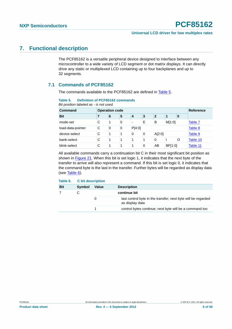
7.1 Commands of PCF85162
The commands available to the PCF85162 are defined in Table 5.
All available commands carry a continuation bit C in their most significant bit position as shown in Figure 21. When this bit is set logic 1, it indicates that the next byte of the transfer to arrive will also represent a command. If this bit is set logic 0, it indicates that the command byte is the last in the transfer. Further bytes will be regarded as display data (see Table 6).
Table 5. Definition of PCF85162 commandsBit position labeled as - is not used.
Command Operation code Reference
Bit 7 6 5 4 3 2 1 0
mode-set C 1 0 - E B M[1:0] Table 7
load-data-pointer C 0 0 P[4:0] Table 8
device-select C 1 1 0 0 A[2:0] Table 9
bank-select C 1 1 1 1 0 I O Table 10
blink-select C 1 1 1 0 AB BF[1:0] Table 11
Table 6. C bit description
Bit Symbol Value Description
7 C continue bit
0 last control byte in the transfer; next byte will be regarded as display data
1 control bytes continue; next byte will be a command too
PCF85162 All information provided in this document is subject to legal disclaimers. © NXP B.V. 2012. All rights reserved.
Product data sheet Rev. 4 — 5 September 2012 7 of 56
NXP Semiconductors PCF85162Universal LCD driver for low multiplex rates
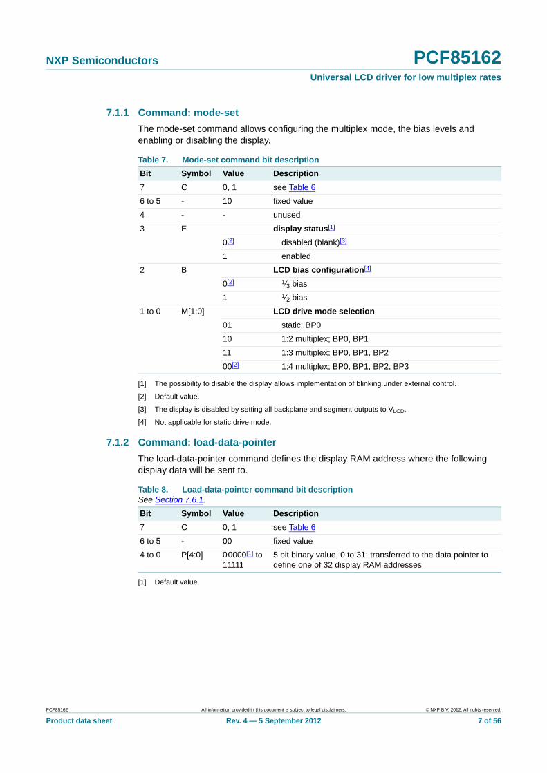
7.1.1 Command: mode-set
The mode-set command allows configuring the multiplex mode, the bias levels and enabling or disabling the display.
[1] The possibility to disable the display allows implementation of blinking under external control.
[2] Default value.
[3] The display is disabled by setting all backplane and segment outputs to VLCD.
[4] Not applicable for static drive mode.
7.1.2 Command: load-data-pointer
The load-data-pointer command defines the display RAM address where the following display data will be sent to.
[1] Default value.
Table 7. Mode-set command bit description
Bit Symbol Value Description
7 C 0, 1 see Table 6
6 to 5 - 10 fixed value
4 - - unused
3 E display status[1]
0[2] disabled (blank)[3]
1 enabled
2 B LCD bias configuration[4]
0[2] 1⁄3 bias
1 1⁄2 bias
1 to 0 M[1:0] LCD drive mode selection
01 static; BP0
10 1:2 multiplex; BP0, BP1
11 1:3 multiplex; BP0, BP1, BP2
00[2] 1:4 multiplex; BP0, BP1, BP2, BP3
Table 8. Load-data-pointer command bit descriptionSee Section 7.6.1.
Bit Symbol Value Description
7 C 0, 1 see Table 6
6 to 5 - 00 fixed value
4 to 0 P[4:0] 00000[1] to11111
5 bit binary value, 0 to 31; transferred to the data pointer to define one of 32 display RAM addresses
PCF85162 All information provided in this document is subject to legal disclaimers. © NXP B.V. 2012. All rights reserved.
Product data sheet Rev. 4 — 5 September 2012 8 of 56
NXP Semiconductors PCF85162Universal LCD driver for low multiplex rates
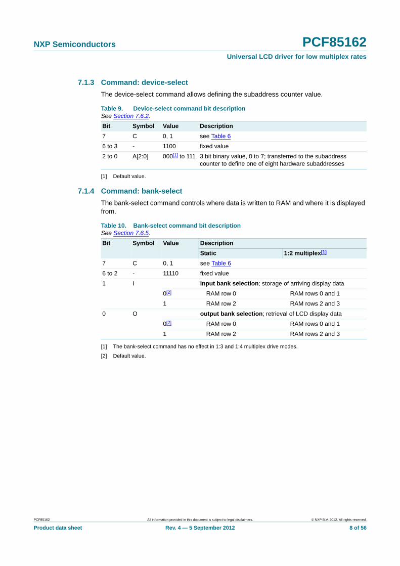
7.1.3 Command: device-select
The device-select command allows defining the subaddress counter value.
[1] Default value.
7.1.4 Command: bank-select
The bank-select command controls where data is written to RAM and where it is displayed from.
[1] The bank-select command has no effect in 1:3 and 1:4 multiplex drive modes.
[2] Default value.
Table 9. Device-select command bit descriptionSee Section 7.6.2.
Bit Symbol Value Description
7 C 0, 1 see Table 6
6 to 3 - 1100 fixed value
2 to 0 A[2:0] 000[1] to 111 3 bit binary value, 0 to 7; transferred to the subaddress counter to define one of eight hardware subaddresses
Table 10. Bank-select command bit descriptionSee Section 7.6.5.
Bit Symbol Value Description
Static 1:2 multiplex[1]
7 C 0, 1 see Table 6
6 to 2 - 11110 fixed value
1 I input bank selection; storage of arriving display data
0[2] RAM row 0 RAM rows 0 and 1
1 RAM row 2 RAM rows 2 and 3
0 O output bank selection; retrieval of LCD display data
0[2] RAM row 0 RAM rows 0 and 1
1 RAM row 2 RAM rows 2 and 3
PCF85162 All information provided in this document is subject to legal disclaimers. © NXP B.V. 2012. All rights reserved.
Product data sheet Rev. 4 — 5 September 2012 9 of 56
NXP Semiconductors PCF85162Universal LCD driver for low multiplex rates
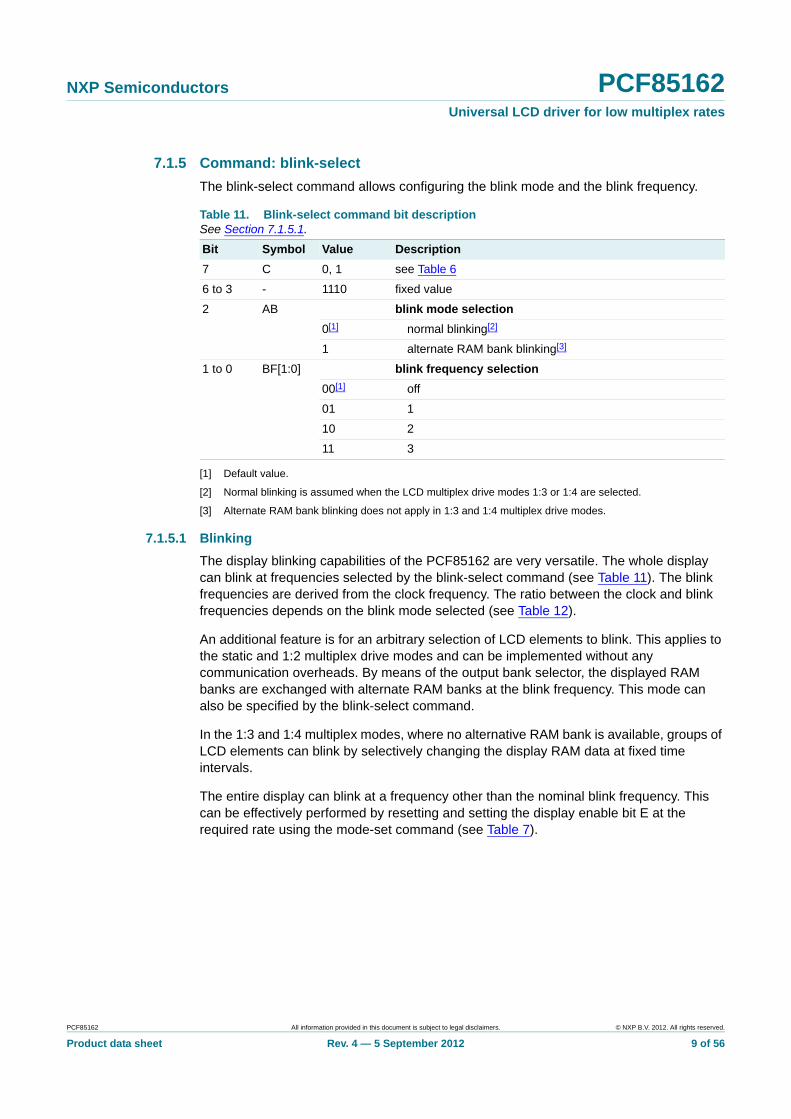
7.1.5 Command: blink-select
The blink-select command allows configuring the blink mode and the blink frequency.
[1] Default value.
[2] Normal blinking is assumed when the LCD multiplex drive modes 1:3 or 1:4 are selected.
[3] Alternate RAM bank blinking does not apply in 1:3 and 1:4 multiplex drive modes.
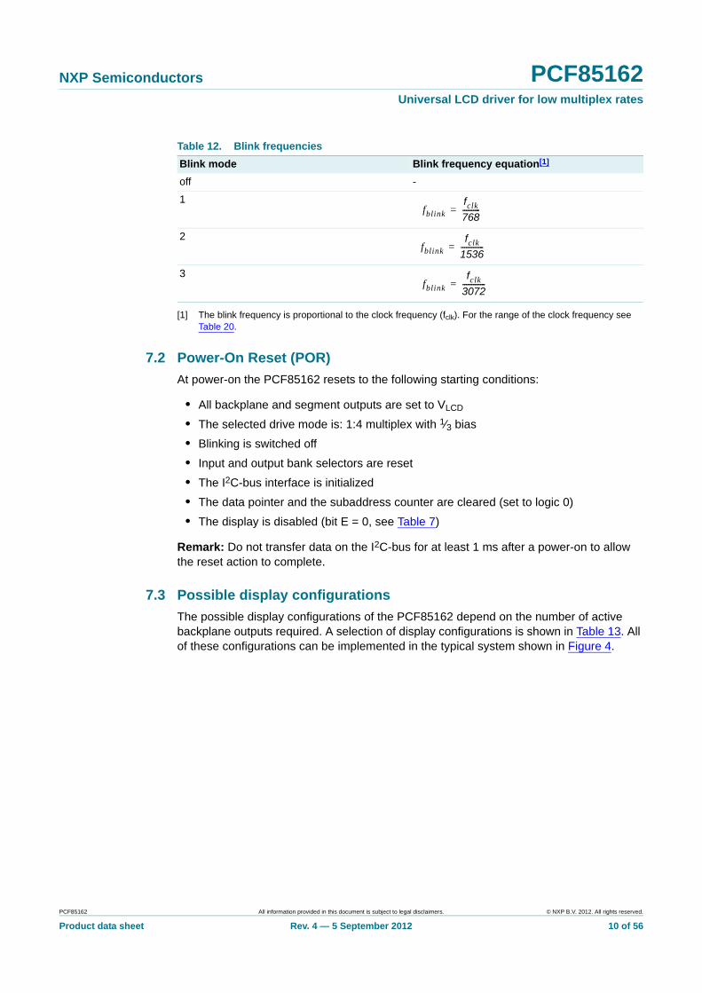
7.1.5.1 Blinking
The display blinking capabilities of the PCF85162 are very versatile. The whole display can blink at frequencies selected by the blink-select command (see Table 11). The blink frequencies are derived from the clock frequency. The ratio between the clock and blink frequencies depends on the blink mode selected (see Table 12).
An additional feature is for an arbitrary selection of LCD elements to blink. This applies to the static and 1:2 multiplex drive modes and can be implemented without any communication overheads. By means of the output bank selector, the displayed RAM banks are exchanged with alternate RAM banks at the blink frequency. This mode can also be specified by the blink-select command.
In the 1:3 and 1:4 multiplex modes, where no alternative RAM bank is available, groups of LCD elements can blink by selectively changing the display RAM data at fixed time intervals.
The entire display can blink at a frequency other than the nominal blink frequency. This can be effectively performed by resetting and setting the display enable bit E at the required rate using the mode-set command (see Table 7).
Table 11. Blink-select command bit descriptionSee Section 7.1.5.1.
Bit Symbol Value Description
7 C 0, 1 see Table 6
6 to 3 - 1110 fixed value
2 AB blink mode selection
0[1] normal blinking[2]
1 alternate RAM bank blinking[3]
1 to 0 BF[1:0] blink frequency selection
00[1] off
01 1
10 2
11 3
PCF85162 All information provided in this document is subject to legal disclaimers. © NXP B.V. 2012. All rights reserved.
Product data sheet Rev. 4 — 5 September 2012 10 of 56
NXP Semiconductors PCF85162Universal LCD driver for low multiplex rates
[1] The blink frequency is proportional to the clock frequency (fclk). For the range of the clock frequency see Table 20.
7.2 Power-On Reset (POR)
At power-on the PCF85162 resets to the following starting conditions:
• All backplane and segment outputs are set to VLCD
• The selected drive mode is: 1:4 multiplex with 1⁄3 bias
• Blinking is switched off
• Input and output bank selectors are reset
• The I2C-bus interface is initialized
• The data pointer and the subaddress counter are cleared (set to logic 0)
• The display is disabled (bit E = 0, see Table 7)
Remark: Do not transfer data on the I2C-bus for at least 1 ms after a power-on to allow the reset action to complete.
7.3 Possible display configurations
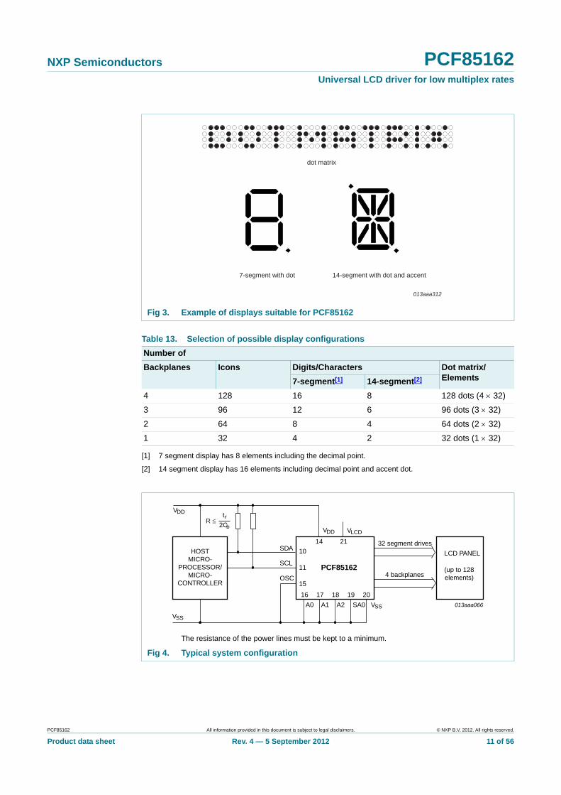
The possible display configurations of the PCF85162 depend on the number of active backplane outputs required. A selection of display configurations is shown in Table 13. All of these configurations can be implemented in the typical system shown in Figure 4.
Table 12. Blink frequencies
Blink mode Blink frequency equation[1]
off -
1
2
3
fblink
fclk
768----------=
fblink
fclk
1536-------------=
fblink
fclk
3072-------------=
PCF85162 All information provided in this document is subject to legal disclaimers. © NXP B.V. 2012. All rights reserved.
Product data sheet Rev. 4 — 5 September 2012 11 of 56
NXP Semiconductors PCF85162Universal LCD driver for low multiplex rates
[1] 7 segment display has 8 elements including the decimal point.
[2] 14 segment display has 16 elements including decimal point and accent dot.
Fig 3. Example of displays suitable for PCF85162
Table 13. Selection of possible display configurations
Number of
Backplanes Icons Digits/Characters Dot matrix/Elements7-segment[1] 14-segment[2]
4 128 16 8 128 dots (4 32)
3 96 12 6 96 dots (3 32)
2 64 8 4 64 dots (2 32)
1 32 4 2 32 dots (1 32)
The resistance of the power lines must be kept to a minimum.
Fig 4. Typical system configuration
7-segment with dot 14-segment with dot and accent
013aaa312
dot matrix
HOSTMICRO-
PROCESSOR/MICRO-
CONTROLLER
tr2Cb
SDA
SCL
OSC
32 segment drives
4 backplanes
LCD PANEL
(up to 128elements)
PCF85162
A0
16
15
11
10
14 21
17 18 19 20
A1 A2 SA0
VDD
VSS
VSS
VDD VLCD
013aaa066
R ≤
PCF85162 All information provided in this document is subject to legal disclaimers. © NXP B.V. 2012. All rights reserved.
Product data sheet Rev. 4 — 5 September 2012 12 of 56
NXP Semiconductors PCF85162Universal LCD driver for low multiplex rates
The host microcontroller maintains the 2-line I2C-bus communication channel with the PCF85162. The internal oscillator is enabled by connecting pin OSC to pin VSS. The appropriate biasing voltages for the multiplexed LCD waveforms are generated internally. The only other connections required to complete the system are the power supplies (VDD, VSS, and VLCD) and the LCD panel chosen for the application.
7.3.1 LCD bias generator
Fractional LCD biasing voltages are obtained from an internal voltage divider consisting of three impedances connected in series between VLCD and VSS. The center impedance is bypassed by switch if the 1⁄2 bias voltage level for the 1:2 multiplex drive mode configuration is selected. The LCD voltage can be temperature compensated externally, using the supply to pin VLCD.
7.3.2 Display register
The display register holds the display data while the corresponding multiplex signals are generated.
7.3.3 LCD voltage selector
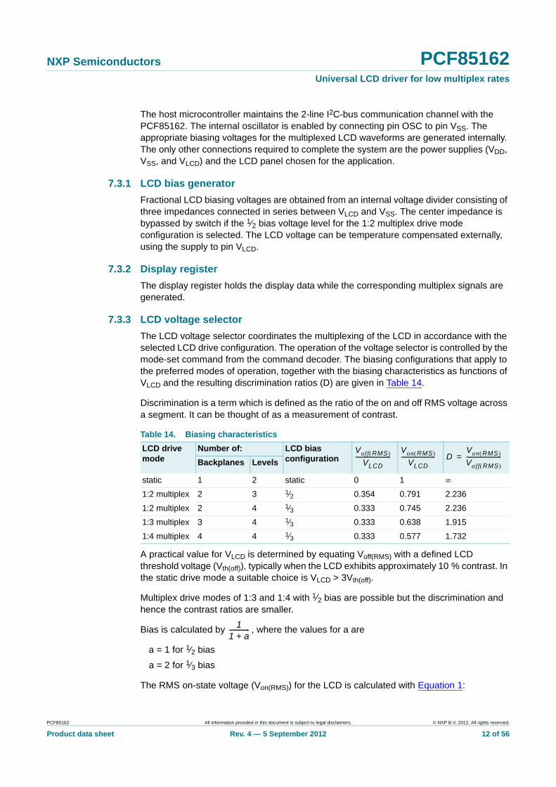
The LCD voltage selector coordinates the multiplexing of the LCD in accordance with the selected LCD drive configuration. The operation of the voltage selector is controlled by the mode-set command from the command decoder. The biasing configurations that apply to the preferred modes of operation, together with the biasing characteristics as functions of VLCD and the resulting discrimination ratios (D) are given in Table 14.
Discrimination is a term which is defined as the ratio of the on and off RMS voltage across a segment. It can be thought of as a measurement of contrast.
A practical value for VLCD is determined by equating Voff(RMS) with a defined LCD threshold voltage (Vth(off)), typically when the LCD exhibits approximately 10 % contrast. In the static drive mode a suitable choice is VLCD > 3Vth(off).
Multiplex drive modes of 1:3 and 1:4 with 1⁄2 bias are possible but the discrimination and hence the contrast ratios are smaller.
Bias is calculated by , where the values for a are
a = 1 for 1⁄2 bias
a = 2 for 1⁄3 bias
The RMS on-state voltage (Von(RMS)) for the LCD is calculated with Equation 1:
Table 14. Biasing characteristics
LCD drive mode
Number of: LCD bias configurationBackplanes Levels
static 1 2 static 0 1
1:2 multiplex 2 3 1⁄2 0.354 0.791 2.236
1:2 multiplex 2 4 1⁄3 0.333 0.745 2.236
1:3 multiplex 3 4 1⁄3 0.333 0.638 1.915
1:4 multiplex 4 4 1⁄3 0.333 0.577 1.732
Voff RMS VLCD
-------------------------Von RMS
VLCD------------------------ D
Von RMS Voff RMS -------------------------=
11 a+-------------
PCF85162 All information provided in this document is subject to legal disclaimers. © NXP B.V. 2012. All rights reserved.
Product data sheet Rev. 4 — 5 September 2012 13 of 56
NXP Semiconductors PCF85162Universal LCD driver for low multiplex rates
(1)
where the values for n are
n = 1 for static drive mode
n = 2 for 1:2 multiplex drive mode
n = 3 for 1:3 multiplex drive mode
n = 4 for 1:4 multiplex drive mode
The RMS off-state voltage (Voff(RMS)) for the LCD is calculated with Equation 2:
(2)
Discrimination is the ratio of Von(RMS) to Voff(RMS) and is determined from Equation 3:
(3)
Using Equation 3, the discrimination for an LCD drive mode of 1:3 multiplex with 1⁄2 bias is and the discrimination for an LCD drive mode of 1:4 multiplex with
1⁄2 bias is .
The advantage of these LCD drive modes is a reduction of the LCD full scale voltage VLCD as follows:
• 1:3 multiplex (1⁄2 bias):
• 1:4 multiplex (1⁄2 bias):
These compare with when 1⁄3 bias is used.
It should be noted that VLCD is sometimes referred as the LCD operating voltage.
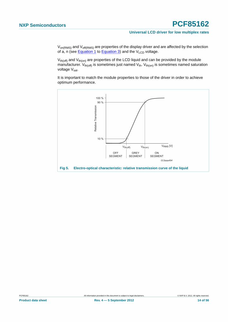
7.3.3.1 Electro-optical performance
Suitable values for Von(RMS) and Voff(RMS) are dependent on the LCD liquid used. The RMS voltage, at which a pixel will be switched on or off, determine the transmissibility of the pixel.
For any given liquid, there are two threshold values defined. One point is at 10 % relative transmission (at Vth(off)) and the other at 90 % relative transmission (at Vth(on)), see Figure 5. For a good contrast performance, the following rules should be followed:
(4)
(5)
Von RMS a2 2a n+ +
n 1 a+ 2------------------------------VLCD
=
Voff RMS a2 2a– n+
n 1 a+ 2------------------------------VLCD
=
DVon RMS
Voff RMS ----------------------- a
22a n+ +
a2
2a– n+---------------------------= =
3 1.732=
213
---------- 1.528=
VLCD 6 Voff RMS 2.449Voff RMS = =
VLCD4 3
3---------------------- 2.309Voff RMS = =
VLCD 3Voff RMS =
Von RMS Vth on
Voff RMS Vth off
PCF85162 All information provided in this document is subject to legal disclaimers. © NXP B.V. 2012. All rights reserved.
Product data sheet Rev. 4 — 5 September 2012 14 of 56
NXP Semiconductors PCF85162Universal LCD driver for low multiplex rates
Von(RMS) and Voff(RMS) are properties of the display driver and are affected by the selection of a, n (see Equation 1 to Equation 3) and the VLCD voltage.
Vth(off) and Vth(on) are properties of the LCD liquid and can be provided by the module manufacturer. Vth(off) is sometimes just named Vth. Vth(on) is sometimes named saturation voltage Vsat.
It is important to match the module properties to those of the driver in order to achieve optimum performance.
Fig 5. Electro-optical characteristic: relative transmission curve of the liquid
VRMS [V]
100 %90 %
10 %
OFFSEGMENT
GREYSEGMENT
ONSEGMENT
Vth(off) Vth(on)
Rel
ativ
e Tr
ansm
issi
on
013aaa494
PCF85162 All information provided in this document is subject to legal disclaimers. © NXP B.V. 2012. All rights reserved.
Product data sheet Rev. 4 — 5 September 2012 15 of 56
NXP Semiconductors PCF85162Universal LCD driver for low multiplex rates
7.3.4 LCD drive mode waveforms
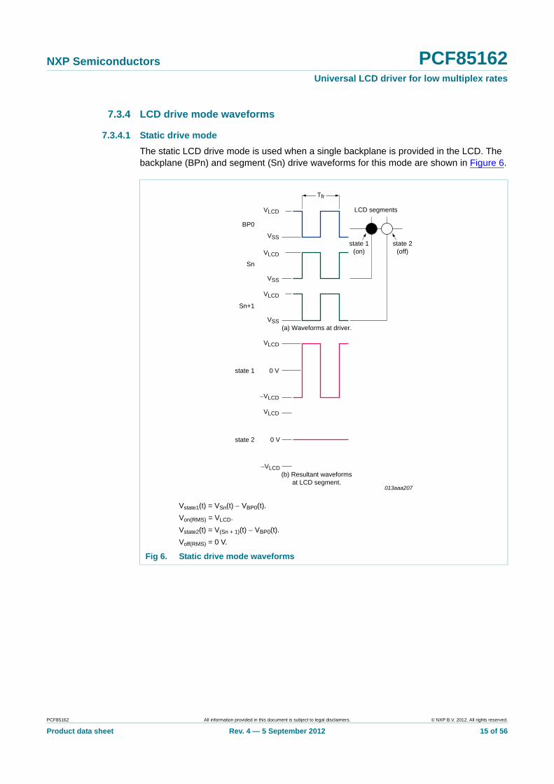
7.3.4.1 Static drive mode
The static LCD drive mode is used when a single backplane is provided in the LCD. The backplane (BPn) and segment (Sn) drive waveforms for this mode are shown in Figure 6.
Vstate1(t) = VSn(t) VBP0(t).
Von(RMS) = VLCD.
Vstate2(t) = V(Sn + 1)(t) VBP0(t).
Voff(RMS) = 0 V.
Fig 6. Static drive mode waveforms
013aaa207
VSS
VLCD
VSS
VLCD
VSS
VLCD
VLCD
−VLCD
−VLCD
VLCD
state 1 0 V
BP0
Sn
Sn+1
state 2 0 V
(a) Waveforms at driver.
(b) Resultant waveformsat LCD segment.
LCD segments
state 1(on)
state 2(off)
Tfr
PCF85162 All information provided in this document is subject to legal disclaimers. © NXP B.V. 2012. All rights reserved.
Product data sheet Rev. 4 — 5 September 2012 16 of 56
NXP Semiconductors PCF85162Universal LCD driver for low multiplex rates
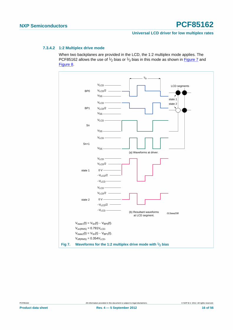
7.3.4.2 1:2 Multiplex drive mode
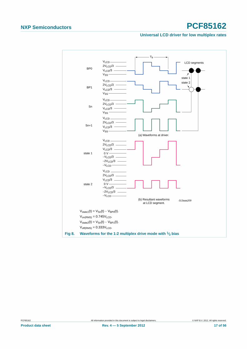
When two backplanes are provided in the LCD, the 1:2 multiplex mode applies. The PCF85162 allows the use of 1⁄2 bias or 1⁄3 bias in this mode as shown in Figure 7 and Figure 8.
Vstate1(t) = VSn(t) VBP0(t).
Von(RMS) = 0.791VLCD.
Vstate2(t) = VSn(t) VBP1(t).
Voff(RMS) = 0.354VLCD.
Fig 7. Waveforms for the 1:2 multiplex drive mode with 1⁄2 bias
013aaa208
state 1
BP0
(a) Waveforms at driver.
(b) Resultant waveformsat LCD segment.
LCD segments
state 2
BP1
state 2
state 1VSS
VLCD
VLCD/2
VSS
VSS
VLCD
VLCD
VSS
VLCD
VLCD
VLCD
0 V
0 V
VLCD/2
VLCD/2
VLCD/2
−VLCD
−VLCD
−VLCD/2
−VLCD/2
Sn
Sn+1
Tfr
PCF85162 All information provided in this document is subject to legal disclaimers. © NXP B.V. 2012. All rights reserved.
Product data sheet Rev. 4 — 5 September 2012 17 of 56
NXP Semiconductors PCF85162Universal LCD driver for low multiplex rates
Vstate1(t) = VSn(t) VBP0(t).
Von(RMS) = 0.745VLCD.
Vstate2(t) = VSn(t) VBP1(t).
Voff(RMS) = 0.333VLCD.
Fig 8. Waveforms for the 1:2 multiplex drive mode with 1⁄3 bias
013aaa209
state 1
BP0
(a) Waveforms at driver.
(b) Resultant waveformsat LCD segment.
LCD segments
state 2
BP1
state 1
state 2
VSS
VLCD
2VLCD/3
VLCD/3
VSS
VLCD
2VLCD/3
VLCD/3
VSS
VLCD
2VLCD/3
VLCD/3
0 V
VLCD
2VLCD/3
−2VLCD/3
VLCD/3
−VLCD/3
−VLCD
−VLCD
0 V
VLCD
2VLCD/3
−2VLCD/3
VLCD/3
−VLCD/3
Sn
Sn+1
Tfr
VSS
VLCD
2VLCD/3
VLCD/3
PCF85162 All information provided in this document is subject to legal disclaimers. © NXP B.V. 2012. All rights reserved.
Product data sheet Rev. 4 — 5 September 2012 18 of 56
NXP Semiconductors PCF85162Universal LCD driver for low multiplex rates
7.3.4.3 1:3 Multiplex drive mode
When three backplanes are provided in the LCD, the 1:3 multiplex drive mode applies, as shown in Figure 9.
Vstate1(t) = VSn(t) VBP0(t).
Von(RMS) = 0.638VLCD.
Vstate2(t) = VSn(t) VBP1(t).
Voff(RMS) = 0.333VLCD.
Fig 9. Waveforms for the 1:3 multiplex drive mode with 1⁄3 bias
013aaa210
state 1
BP0
(b) Resultant waveformsat LCD segment.
LCD segments
state 2
BP1
state 1
state 2
(a) Waveforms at driver.
BP2
Sn
Sn+1
Sn+2
Tfr
VSS
VLCD
2VLCD/3
VLCD/3
VSS
VLCD
2VLCD/3
VLCD/3
VSS
VLCD
2VLCD/3
VLCD/3
VSS
VLCD
2VLCD/3
VLCD/3
VSS
VLCD
2VLCD/3
VLCD/3
0 V
VLCD
2VLCD/3
−2VLCD/3
VLCD/3
−VLCD/3
−VLCD
0 V
VLCD
2VLCD/3
−2VLCD/3
VLCD/3
−VLCD/3
−VLCD
VSS
VLCD
2VLCD/3
VLCD/3
PCF85162 All information provided in this document is subject to legal disclaimers. © NXP B.V. 2012. All rights reserved.
Product data sheet Rev. 4 — 5 September 2012 19 of 56
NXP Semiconductors PCF85162Universal LCD driver for low multiplex rates
7.3.4.4 1:4 Multiplex drive mode
When four backplanes are provided in the LCD, the 1:4 multiplex drive mode applies as shown in Figure 10.
Vstate1(t) = VSn(t) VBP0(t).
Von(RMS) = 0.577VLCD.
Vstate2(t) = VSn(t) VBP1(t).
Voff(RMS) = 0.333VLCD.
Fig 10. Waveforms for the 1:4 multiplex drive mode with 1⁄3 bias
013aaa211
state 1
BP0
(b) Resultant waveformsat LCD segment.
LCD segments
state 2BP1
state 1
state 2
BP2
(a) Waveforms at driver.
BP3
Sn
Sn+1
Sn+2
Sn+3
Tfr
VSS
VLCD2VLCD/3VLCD/3
VSS
VLCD2VLCD/3VLCD/3
VSS
VLCD2VLCD/3VLCD/3
VSS
VLCD2VLCD/3VLCD/3
VSS
VLCD2VLCD/3VLCD/3
VSS
VLCD2VLCD/3VLCD/3
VSS
VLCD2VLCD/3VLCD/3
0 V
VLCD2VLCD/3
-2VLCD/3
VLCD/3
-VLCD/3
-VLCD
0 V
VLCD2VLCD/3
-2VLCD/3
VLCD/3
-VLCD/3
-VLCD
VSS
VLCD2VLCD/3VLCD/3
PCF85162 All information provided in this document is subject to legal disclaimers. © NXP B.V. 2012. All rights reserved.
Product data sheet Rev. 4 — 5 September 2012 20 of 56
NXP Semiconductors PCF85162Universal LCD driver for low multiplex rates
7.4 Oscillator
7.4.1 Internal clock
The internal logic of the PCF85162 and its LCD drive signals are timed either by its internal oscillator or by an external clock. The internal oscillator is enabled by connecting pin OSC to pin VSS. If the internal oscillator is used, the output from pin CLK can be used as the clock signal for several PCF85162 in the system that are connected in cascade.
7.4.2 External clock
Pin CLK is enabled as an external clock input by connecting pin OSC to VDD. The LCD frame frequency is determined by the clock frequency (fclk).
Remark: A clock signal must always be supplied to the device; removing the clock may freeze the LCD in a DC state, which is not suitable for the liquid crystal.
7.4.3 Timing
The PCF85162 timing controls the internal data flow of the device. This includes the transfer of display data from the display RAM to the display segment outputs. In cascaded applications, the correct timing relationship between each PCF85162 in the system is maintained by the synchronization signal at pin SYNC. The timing also generates the LCD frame frequency signal. The frame frequency signal is a fixed division of the clock
frequency from either the internal or an external clock:
7.5 Backplane and segment outputs
7.5.1 Backplane outputs
The LCD drive section includes four backplane outputs BP0 to BP3 which must be connected directly to the LCD. The backplane output signals are generated in accordance with the selected LCD drive mode. If less than four backplane outputs are required, the unused outputs can be left open-circuit.
• In 1:3 multiplex drive mode, BP3 carries the same signal as BP1, therefore these two adjacent outputs can be tied together to give enhanced drive capabilities
• In 1:2 multiplex drive mode, BP0 and BP2, respectively, BP1 and BP3 carry the same signals and may also be paired to increase the drive capabilities
• In static drive mode the same signal is carried by all four backplane outputs and they can be connected in parallel for very high drive requirements
7.5.2 Segment outputs
The LCD drive section includes 32 segment outputs (S0 to S31) which should be connected directly to the LCD. The segment output signals are generated in accordance with the multiplexed backplane signals and with data residing in the display register. When less than 32 segment outputs are required, the unused segment outputs should be left open-circuit.
ffr
fclk
24-------=
PCF85162 All information provided in this document is subject to legal disclaimers. © NXP B.V. 2012. All rights reserved.
Product data sheet Rev. 4 — 5 September 2012 21 of 56
NXP Semiconductors PCF85162Universal LCD driver for low multiplex rates
7.6 Display RAM
The display RAM is a static 32 4-bit RAM which stores LCD data. There is a one-to-one correspondence between
• the bits in the RAM bitmap and the LCD elements
• the RAM columns and the segment outputs
• the RAM rows and the backplane outputs.
A logic 1 in the RAM bitmap indicates the on-state of the corresponding LCD element; similarly, a logic 0 indicates the off-state.
The display RAM bitmap, Figure 11, shows the rows 0 to 3 which correspond with the backplane outputs BP0 to BP3, and the columns 0 to 31 which correspond with the segment outputs S0 to S31. In multiplexed LCD applications the segment data of the first, second, third, and fourth row of the display RAM are time-multiplexed with BP0, BP1, BP2, and BP3 respectively.
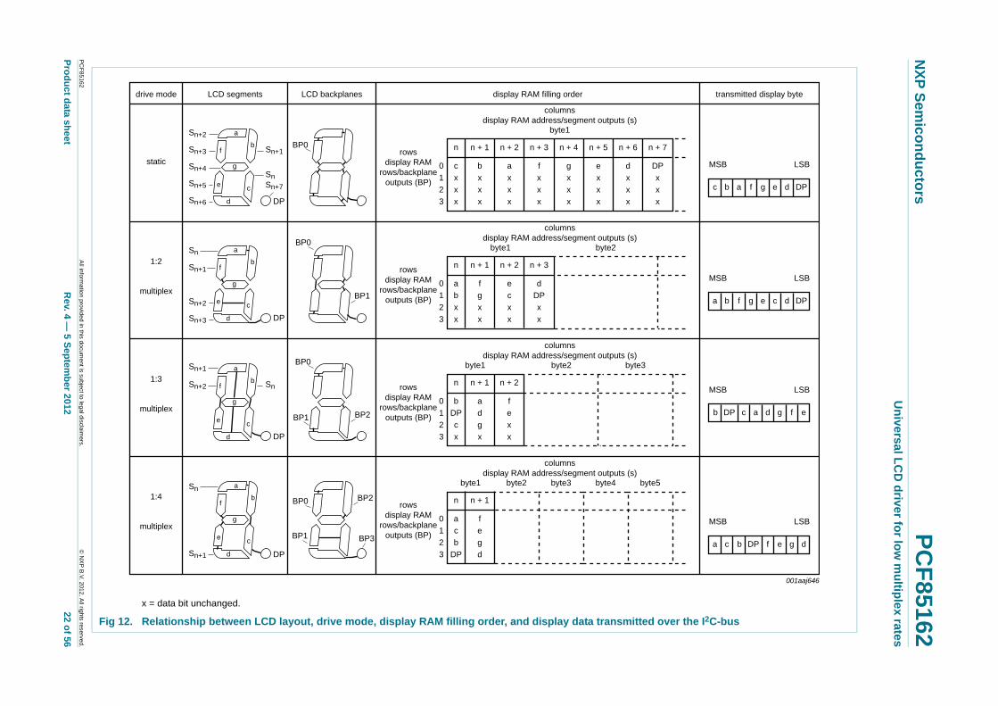
When display data is transmitted to the PCF85162, the display bytes received are stored in the display RAM in accordance with the selected LCD drive mode. The data is stored as it arrives and depending on the current multiplex drive mode the bits are stored singularly, in pairs, triples or quadruples. To illustrate the filling order, an example of a 7-segment numeric display showing all drive modes is given in Figure 12; the RAM filling organization depicted applies equally to other LCD types.
• In static drive mode the eight transmitted data bits are placed into row 0 as one byte
• In 1:2 multiplex drive mode the eight transmitted data bits are placed in pairs into row 0 and 1 as two successive 4-bit RAM words
• In 1:3 multiplex drive mode the eight bits are placed in triples into row 0, 1, and 2 as three successive 3-bit RAM words, with bit 3 of the third address left unchanged. It is not recommended to use this bit in a display because of the difficult addressing. This last bit may, if necessary, be controlled by an additional transfer to this address, but care should be taken to avoid overwriting adjacent data because always full bytes are transmitted (see Section 7.6.4)
• In 1:4 multiplex drive mode, the eight transmitted data bits are placed in quadruples into row 0, 1, 2, and 3 as two successive 4-bit RAM words
The display RAM bitmap shows the direct relationship between the display RAM column and the segment outputs; and between the bits in a RAM row and the backplane outputs.
Fig 11. Display RAM bitmap
0
0
1
2
3
1 2 3 4 27 28 29 30 31
display RAM addresses/segment outputs (S)
columns
display RAM rows/backplane outputs
(BP)
rows
001aac265
xxxxxxxxxxxxxxxxxxxxx xxxxxxxxxxxxxxxxxxxxxxxxxx xxxxxxx x x x xxxxxxxxxxxxxxxxxxxxxxxxxxxxxx xxxxxxxxxxxxxxxxxxx xx xx xxxxx xxxxxxxxxxxxxxxxxxxxxxxxxxx xxxxxxxxxxxxxxxxxxx xxxxxx xxxxxxxxxxxxxxxxxxxxxxxxxxxxxxxxxxx xxxxxxxxxxxx x x xxxxxxxxxxxxxxxxxxxxx xxxxxxxxxxxxxxxxxxxxxxxxxxxxxx xxxxx xxxxxxxxxxxxxxxxxxxxxxxxxxxxxxxxxxxxxxxxxxxxxxxxxx xxxxxxxx xxxxxxxxxxxxxxxxxxxxxxxxx xxxxxxxxxxxxxxxxxxxx xxx
PC
F85
162A
ll information
provided in this do
cument is sub
ject to legal d
isclaimers.
© N
XP
B.V
. 2012. All rig
hts reserved.
Pro
du
ct data sh
eetR
ev. 4 — 5 S
ep
temb
er 2012
22 of 56
NX
P S
emico
nd
ucto
rsP
CF
85162U
niv
ers
al L
CD
drive
r for lo
w m
ultip
lex
rates
x = data bit unchanged.
Fig 12. Relationship between LCD layout, drive mode, display RAM filling order, and display data transmitted over the I2C-bus
001aaj646
a c b DP f e g d
MSB LSB
b DP c a d g f e
MSB LSB
a b f g e c d DP
MSB LSB
c b a f g e d DP
MSB LSB
drive mode
static
1:2
multiplex
1:3
multiplex
1:4
multiplex
LCD segments LCD backplanes display RAM filling order transmitted display byte
BP0
BP0
BP1
BP0
BP1 BP2
BP1
BP2
BP3
BP0
n
cxxx
0123
bxxx
axxx
fxxx
gxxx
exxx
dxxx
DPxxx
n + 1 n + 2 n + 3 n + 4 n + 5 n + 6 n + 7rowsdisplay RAM
rows/backplaneoutputs (BP)
byte1
columnsdisplay RAM address/segment outputs (s)
n
abxx
0123
fgxx
ecxx
dDPxx
n + 1 n + 2 n + 3
byte1 byte2
rowsdisplay RAM
rows/backplaneoutputs (BP)
columnsdisplay RAM address/segment outputs (s)
n
bDPcx
0123
adgx
fexx
n + 1 n + 2
byte1 byte2 byte3
rowsdisplay RAM
rows/backplaneoutputs (BP)
columnsdisplay RAM address/segment outputs (s)
n + 1n
acb
DP
0123
fegd
byte1 byte2 byte3 byte4 byte5
rowsdisplay RAM
rows/backplaneoutputs (BP)
columnsdisplay RAM address/segment outputs (s)
Sn+2
Sn+3
Sn+1
Sn
DP
a
fb
g
e c
d
Sn+2
Sn+1
Sn+7
Sn
Sn+3
Sn+5
Sn+6
Sn+4
DP
a
fb
g
e c
d
Sn
Sn+1
Sn+2
DP
a
fb
g
e c
d
Sn+1
Sn
DP
a
fb
g
e c
d
PCF85162 All information provided in this document is subject to legal disclaimers. © NXP B.V. 2012. All rights reserved.
Product data sheet Rev. 4 — 5 September 2012 23 of 56
NXP Semiconductors PCF85162Universal LCD driver for low multiplex rates
7.6.1 Data pointer
The addressing mechanism for the display RAM is realized using the data pointer. This allows the loading of an individual display data byte, or a series of display data bytes, into any location of the display RAM. The sequence commences with the initialization of the data pointer by the load-data-pointer command (see Table 8). Following this command, an arriving data byte is stored at the display RAM address indicated by the data pointer. The filling order is shown in Figure 12.
After each byte is stored, the content of the data pointer is automatically incremented by a value dependent on the selected LCD drive mode:
• In static drive mode by eight
• In 1:2 multiplex drive mode by four
• In 1:3 multiplex drive mode by three
• In 1:4 multiplex drive mode by two
If an I2C-bus data access terminates early then the state of the data pointer is unknown. Consequently, the data pointer must be rewritten prior to further RAM accesses.
7.6.2 Subaddress counter
The storage of display data is determined by the contents of the subaddress counter. Storage is allowed only when the content of the subaddress counter match with the hardware subaddress applied to A0, A1, and A2. The subaddress counter value is defined by the device-select command (see Table 9). If the content of the subaddress counter and the hardware subaddress do not match then data storage is inhibited but the data pointer is incremented as if data storage had taken place. The subaddress counter is also incremented when the data pointer overflows.
7.6.3 RAM addressing in cascaded applications
In cascaded applications each PCF85162 in the cascade must be addressed separately. Initially, the first PCF85162 is selected by sending the device-select command matching the first device's hardware subaddress. Then the data pointer is set to the preferred display RAM address by sending the load-data-pointer command.
Once the display RAM of the first PCF85162 has been written, the second PCF85162 is selected by sending the device-select command again. This time however the command matches the second device's hardware subaddress. Next the load-data-pointer command is sent to select the preferred display RAM address of the second PCF85162.
This last step is very important because during writing data to the first PCF85162, the data pointer of the second PCF85162 is incremented. In addition, the hardware subaddress should not be changed whilst the device is being accessed on the I2C-bus interface.
PCF85162 All information provided in this document is subject to legal disclaimers. © NXP B.V. 2012. All rights reserved.
Product data sheet Rev. 4 — 5 September 2012 24 of 56
NXP Semiconductors PCF85162Universal LCD driver for low multiplex rates
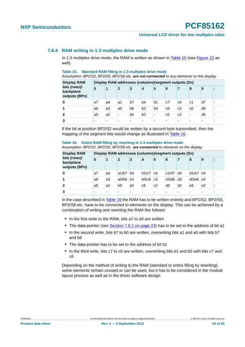
7.6.4 RAM writing in 1:3 multiplex drive mode
In 1:3 multiplex drive mode, the RAM is written as shown in Table 15 (see Figure 12 as well).
If the bit at position BP2/S2 would be written by a second byte transmitted, then the mapping of the segment bits would change as illustrated in Table 16.
In the case described in Table 16 the RAM has to be written entirely and BP2/S2, BP2/S5, BP2/S8 etc. have to be connected to elements on the display. This can be achieved by a combination of writing and rewriting the RAM like follows:
• In the first write to the RAM, bits a7 to a0 are written
• The data-pointer (see Section 7.6.1 on page 23) has to be set to the address of bit a1
• In the second write, bits b7 to b0 are written, overwriting bits a1 and a0 with bits b7 and b6
• The data-pointer has to be set to the address of bit b1
• In the third write, bits c7 to c0 are written, overwriting bits b1 and b0 with bits c7 and c6
Depending on the method of writing to the RAM (standard or entire filling by rewriting), some elements remain unused or can be used, but it has to be considered in the module layout process as well as in the driver software design.
Table 15. Standard RAM filling in 1:3 multiplex drive modeAssumption: BP2/S2, BP2/S5, BP2/S8 etc. are not connected to any elements on the display.
Display RAM bits (rows)/ backplane outputs (BPn)
Display RAM addresses (columns)/segment outputs (Sn)
0 1 2 3 4 5 6 7 8 9 :
0 a7 a4 a1 b7 b4 b1 c7 c4 c1 d7 :
1 a6 a3 a0 b6 b3 b0 c6 c3 c0 d6 :
2 a5 a2 - b5 b2 - c5 c2 - d5 :
3 - - - - - - - - - - :
Table 16. Entire RAM filling by rewriting in 1:3 multiplex drive modeAssumption: BP2/S2, BP2/S5, BP2/S8 etc. are connected to elements on the display.
Display RAM bits (rows)/ backplane outputs (BPn)
Display RAM addresses (columns)/segment outputs (Sn)
0 1 2 3 4 5 6 7 8 9 :
0 a7 a4 a1/b7 b4 b1/c7 c4 c1/d7 d4 d1/e7 e4 :
1 a6 a3 a0/b6 b3 b0/c6 c3 c0/d6 d3 d0/e6 e3 :
2 a5 a2 b5 b2 c5 c2 d5 d2 e5 e2 :
3 - - - - - - - - - - :
PCF85162 All information provided in this document is subject to legal disclaimers. © NXP B.V. 2012. All rights reserved.
Product data sheet Rev. 4 — 5 September 2012 25 of 56
NXP Semiconductors PCF85162Universal LCD driver for low multiplex rates
7.6.5 Bank selection
7.6.5.1 Output bank selector
The output bank selector (see Table 10) selects one of the four rows per display RAM address for transfer to the display register. The actual row selected depends on the particular LCD drive mode in operation and on the instant in the multiplex sequence.
• In 1:4 multiplex mode, all RAM addresses of row 0 are selected, these are followed by the contents of row 1, 2, and then 3
• In 1:3 multiplex mode, rows 0, 1, and 2 are selected sequentially
• In 1:2 multiplex mode, rows 0 and 1 are selected
• In static mode, row 0 is selected
The PCF85162 includes a RAM bank switching feature in the static and 1:2 multiplex drive modes. In the static drive mode, the bank-select command may request the contents of row 2 to be selected for display instead of the contents of row 0. In the 1:2 multiplex mode, the contents of rows 2 and 3 may be selected instead of rows 0 and 1. This gives the provision for preparing display information in an alternative bank and to be able to switch to it once it is assembled.
7.6.5.2 Input bank selector
The input bank selector loads display data into the display RAM in accordance with the selected LCD drive configuration. Display data can be loaded in row 2 in static drive mode or in rows 2 and 3 in 1:2 multiplex drive mode by using the bank-select command (see Table 10). The input bank selector functions independently to the output bank selector.
7.6.5.3 RAM bank switching
The PCF85162 includes a RAM bank switching feature in the static and 1:2 multiplex drive modes. A bank can be thought of as one RAM row or a collection of RAM rows (see Figure 13). The RAM bank switching gives the provision for preparing display information in an alternative bank and to be able to switch to it once it is complete.
PCF85162 All information provided in this document is subject to legal disclaimers. © NXP B.V. 2012. All rights reserved.
Product data sheet Rev. 4 — 5 September 2012 26 of 56
NXP Semiconductors PCF85162Universal LCD driver for low multiplex rates
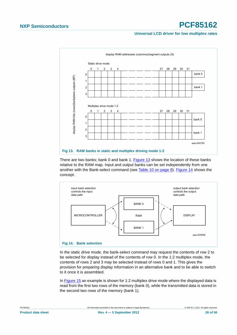
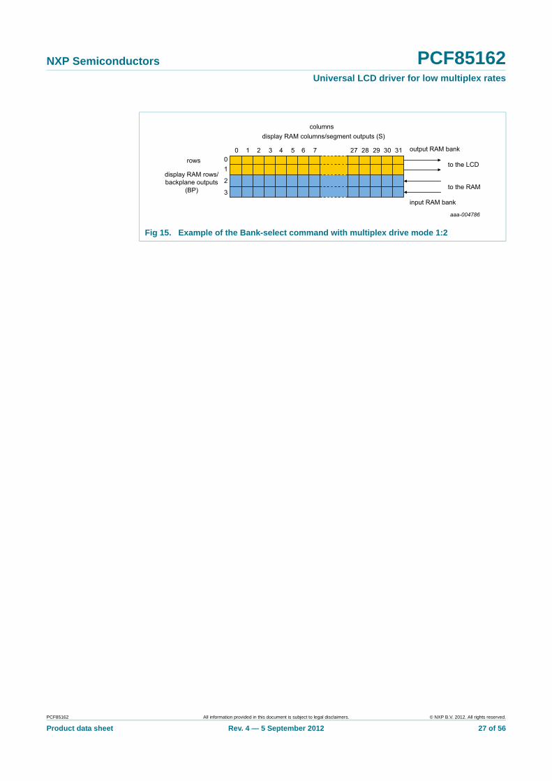
There are two banks; bank 0 and bank 1. Figure 13 shows the location of these banks relative to the RAM map. Input and output banks can be set independently from one another with the Bank-select command (see Table 10 on page 8). Figure 14 shows the concept.
In the static drive mode, the bank-select command may request the contents of row 2 to be selected for display instead of the contents of row 0. In the 1:2 multiplex mode, the contents of rows 2 and 3 may be selected instead of rows 0 and 1. This gives the provision for preparing display information in an alternative bank and to be able to switch to it once it is assembled.
In Figure 15 an example is shown for 1:2 multiplex drive mode where the displayed data is read from the first two rows of the memory (bank 0), while the transmitted data is stored in the second two rows of the memory (bank 1).
Fig 13. RAM banks in static and multiplex driving mode 1:2
Fig 14. Bank selection
�
�
�
�
�
� � � � �� �� � �� ��
�� ��������������������������������!���! �!���"�
��
����
��
��#
�!����
�$��
�#��
& ��
����
�! �
!���'
*�
����������
�
�
�
�
�
� � � � �� �� � �� ��
#��&��
#��&��
#��&��
#��&��
"!�!�����,�����
���!� ��4���,�������5�
������������ ��� �����
������
������
��������
��������������� ��!� !��"!����#�������$�������#��
!��������������� ��!� !��"!����#��!�����$�������#��
PCF85162 All information provided in this document is subject to legal disclaimers. © NXP B.V. 2012. All rights reserved.
Product data sheet Rev. 4 — 5 September 2012 27 of 56
NXP Semiconductors PCF85162Universal LCD driver for low multiplex rates
Fig 15. Example of the Bank-select command with multiplex drive mode 1:2
$�����%����� !��&��'��(&����!�������)�* !��&��
$�����%�����"!+�'��� �������!�������
)� *
"!+�
���������
� � , - . / 0 1 ,1 ,2 ,3 -� -���
,
-
�!��#����
!��������������
��������������
�!��#�����
PCF85162 All information provided in this document is subject to legal disclaimers. © NXP B.V. 2012. All rights reserved.
Product data sheet Rev. 4 — 5 September 2012 28 of 56
NXP Semiconductors PCF85162Universal LCD driver for low multiplex rates
8. Characteristics of the I2C-bus
The I2C-bus is for bidirectional, two-line communication between different ICs or modules. The two lines are a Serial DAta line (SDA) and a Serial CLock line (SCL). Both lines must be connected to a positive supply via a pull-up resistor when connected to the output stages of a device. Data transfer may be initiated only when the bus is not busy.
8.1 Bit transfer
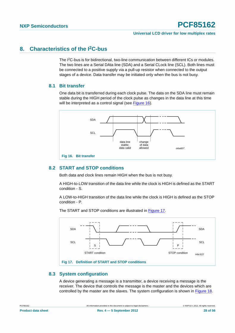
One data bit is transferred during each clock pulse. The data on the SDA line must remain stable during the HIGH period of the clock pulse as changes in the data line at this time will be interpreted as a control signal (see Figure 16).
8.2 START and STOP conditions
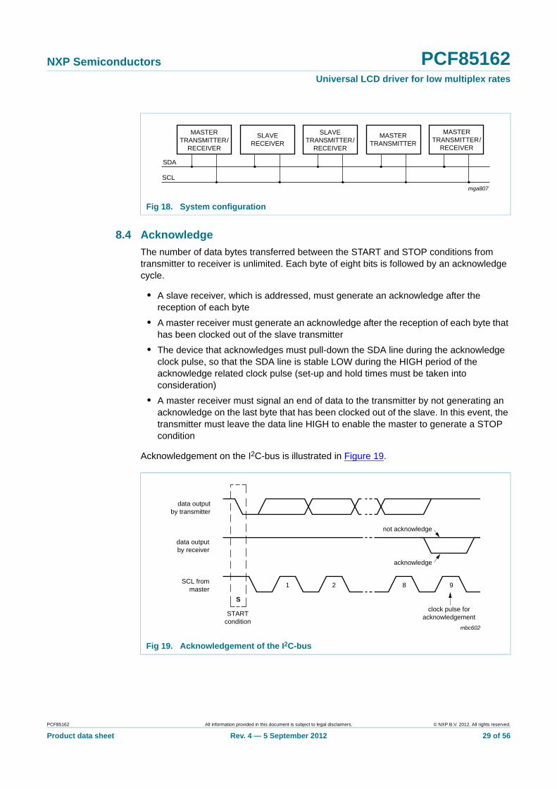
Both data and clock lines remain HIGH when the bus is not busy.
A HIGH-to-LOW transition of the data line while the clock is HIGH is defined as the START condition - S.
A LOW-to-HIGH transition of the data line while the clock is HIGH is defined as the STOP condition - P.
The START and STOP conditions are illustrated in Figure 17.
8.3 System configuration
A device generating a message is a transmitter, a device receiving a message is the receiver. The device that controls the message is the master and the devices which are controlled by the master are the slaves. The system configuration is shown in Figure 18.
Fig 16. Bit transfer
mba607
data linestable;
data valid
changeof dataallowed
SDA
SCL
Fig 17. Definition of START and STOP conditions
mbc622
SDA
SCLP
STOP condition
SDA
SCLS
START condition
PCF85162 All information provided in this document is subject to legal disclaimers. © NXP B.V. 2012. All rights reserved.
Product data sheet Rev. 4 — 5 September 2012 29 of 56
NXP Semiconductors PCF85162Universal LCD driver for low multiplex rates
8.4 Acknowledge
The number of data bytes transferred between the START and STOP conditions from transmitter to receiver is unlimited. Each byte of eight bits is followed by an acknowledge cycle.
• A slave receiver, which is addressed, must generate an acknowledge after the reception of each byte
• A master receiver must generate an acknowledge after the reception of each byte that has been clocked out of the slave transmitter
• The device that acknowledges must pull-down the SDA line during the acknowledge clock pulse, so that the SDA line is stable LOW during the HIGH period of the acknowledge related clock pulse (set-up and hold times must be taken into consideration)
• A master receiver must signal an end of data to the transmitter by not generating an acknowledge on the last byte that has been clocked out of the slave. In this event, the transmitter must leave the data line HIGH to enable the master to generate a STOP condition
Acknowledgement on the I2C-bus is illustrated in Figure 19.
Fig 18. System configuration
mga807
SDA
SCL
MASTERTRANSMITTER/
RECEIVER
MASTERTRANSMITTER
SLAVETRANSMITTER/
RECEIVER
SLAVERECEIVER
MASTERTRANSMITTER/
RECEIVER
Fig 19. Acknowledgement of the I2C-bus
mbc602
S
STARTcondition
9821
clock pulse foracknowledgement
not acknowledge
acknowledge
data outputby transmitter
data outputby receiver
SCL frommaster
PCF85162 All information provided in this document is subject to legal disclaimers. © NXP B.V. 2012. All rights reserved.
Product data sheet Rev. 4 — 5 September 2012 30 of 56
NXP Semiconductors PCF85162Universal LCD driver for low multiplex rates
8.5 I2C-bus controller
The PCF85162 acts as an I2C-bus slave receiver. It does not initiate I2C-bus transfers or transmit data to an I2C-bus master receiver. The only data output from the PCF85162 are the acknowledge signals of the selected devices. Device selection depends on the I2C-bus slave address, on the transferred command data and on the hardware subaddress.
In single device applications, the hardware subaddress inputs A0, A1, and A2 are normally tied to VSS which defines the hardware subaddress 0. In multiple device applications A0, A1, and A2 are tied to VSS or VDD using a binary coding scheme, so that no two devices with a common I2C-bus slave address have the same hardware subaddress.
8.6 Input filters
To enhance noise immunity in electrically adverse environments, RC low-pass filters are provided on the SDA and SCL lines.
8.7 I2C-bus protocol
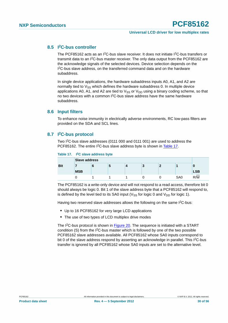
Two I2C-bus slave addresses (0111 000 and 0111 001) are used to address the PCF85162. The entire I2C-bus slave address byte is shown in Table 17.
The PCF85162 is a write-only device and will not respond to a read access, therefore bit 0 should always be logic 0. Bit 1 of the slave address byte that a PCF85162 will respond to, is defined by the level tied to its SA0 input (VSS for logic 0 and VDD for logic 1).
Having two reserved slave addresses allows the following on the same I2C-bus:
• Up to 16 PCF85162 for very large LCD applications
• The use of two types of LCD multiplex drive modes
The I2C-bus protocol is shown in Figure 20. The sequence is initiated with a START condition (S) from the I2C-bus master which is followed by one of the two possible PCF85162 slave addresses available. All PCF85162 whose SA0 inputs correspond to bit 0 of the slave address respond by asserting an acknowledge in parallel. This I2C-bus transfer is ignored by all PCF85162 whose SA0 inputs are set to the alternative level.
Table 17. I2C slave address byte
Slave address
Bit 7 6 5 4 3 2 1 0
MSB LSB
0 1 1 1 0 0 SA0 R/W
PCF85162 All information provided in this document is subject to legal disclaimers. © NXP B.V. 2012. All rights reserved.
Product data sheet Rev. 4 — 5 September 2012 31 of 56
NXP Semiconductors PCF85162Universal LCD driver for low multiplex rates
After an acknowledgement, one or more command bytes follow that define the status of each addressed PCF85162.
The last command byte sent is identified by resetting its most significant bit, continuation bit C (see Figure 21). The command bytes are also acknowledged by all addressed PCF85162 on the bus.
After the last command byte, one or more display data bytes may follow. Display data bytes are stored in the display RAM at the address specified by the data pointer and the subaddress counter. Both data pointer and subaddress counter are automatically updated and the data directed to the intended PCF85162 device.
An acknowledgement after each byte is asserted only by the PCF85162 that are addressed via address lines A0, A1, and A2. After the last display byte, the I2C-bus master asserts a STOP condition (P). Alternately a START may be asserted to restart an I2C-bus access.
Fig 20. I2C-bus protocol
Fig 21. Format of command byte
013aaa235
SA0
S 0 1 1 1 0 0 0 A C COMMAND A PADISPLAY DATA
slave address
R/W
acknowledge byall addressed
PCF85162
acknowledgeby A0, A1 and A2
selectedPCF85162 only
1 byte
update data pointersand if necessary,
subaddress counter
n ≥ 1 byte(s) n ≥ 0 byte(s)
msa833
REST OF OPCODEC
MSB LSB
PCF85162 All information provided in this document is subject to legal disclaimers. © NXP B.V. 2012. All rights reserved.
Product data sheet Rev. 4 — 5 September 2012 32 of 56
NXP Semiconductors PCF85162Universal LCD driver for low multiplex rates
9. Internal circuitry
Fig 22. Device protection circuits
SA0
VDD VDD
VSS VSS
VLCD
VSS
SDA
001aac269
VSS
SCL
VSS
CLK
VDD
VSS
OSC
VDD
VSS
SYNC
VDD
VSS
A0, A1, A2
VDD
VSS
BP0, BP1,BP2, BP3
VLCD
VSS
S0 to S31
VLCD
VSS
PCF85162 All information provided in this document is subject to legal disclaimers. © NXP B.V. 2012. All rights reserved.
Product data sheet Rev. 4 — 5 September 2012 33 of 56
NXP Semiconductors PCF85162Universal LCD driver for low multiplex rates
10. Limiting values
[1] Pass level; Human Body Model (HBM), according to Ref. 6 “JESD22-A114”.
[2] Pass level; Charged-Device Model (CDM), according to Ref. 7 “JESD22-C101”.
[3] Pass level; latch-up testing according to Ref. 8 “JESD78” at maximum ambient temperature (Tamb(max)).
[4] According to the store and transport requirements (see Ref. 12 “UM10569”) the devices have to be stored at a temperature of +8 C to +45 C and a humidity of 25 % to 75 %.
CAUTION
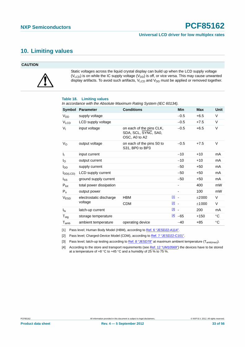
Static voltages across the liquid crystal display can build up when the LCD supply voltage (VLCD) is on while the IC supply voltage (VDD) is off, or vice versa. This may cause unwanted display artifacts. To avoid such artifacts, VLCD and VDD must be applied or removed together.
Table 18. Limiting valuesIn accordance with the Absolute Maximum Rating System (IEC 60134).
Symbol Parameter Conditions Min Max Unit
VDD supply voltage 0.5 +6.5 V
VLCD LCD supply voltage 0.5 +7.5 V
VI input voltage on each of the pins CLK, SDA, SCL, SYNC, SA0, OSC, A0 to A2
0.5 +6.5 V
VO output voltage on each of the pins S0 to S31, BP0 to BP3
0.5 +7.5 V
II input current 10 +10 mA
IO output current 10 +10 mA
IDD supply current 50 +50 mA
IDD(LCD) LCD supply current 50 +50 mA
ISS ground supply current 50 +50 mA
Ptot total power dissipation - 400 mW
Po output power - 100 mW
VESD electrostatic discharge voltage
HBM [1] - 2000 V
CDM [2] - 1000 V
Ilu latch-up current [3] - 200 mA
Tstg storage temperature [4] 65 +150 C
Tamb ambient temperature operating device 40 +85 C
PCF85162 All information provided in this document is subject to legal disclaimers. © NXP B.V. 2012. All rights reserved.
Product data sheet Rev. 4 — 5 September 2012 34 of 56
NXP Semiconductors PCF85162Universal LCD driver for low multiplex rates
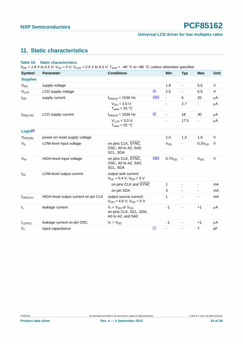
11. Static characteristics
Table 19. Static characteristicsVDD = 1.8 V to 5.5 V; VSS = 0 V; VLCD = 2.5 V to 6.5 V; Tamb = 40 C to +85 C; unless otherwise specified.
Symbol Parameter Conditions Min Typ Max Unit
Supplies
VDD supply voltage 1.8 - 5.5 V
VLCD LCD supply voltage [1] 2.5 - 6.5 V
IDD supply current fclk(ext) = 1536 Hz [2][3] - 6 20 A
VDD = 3.0 V; Tamb = 25 C
- 2.7 - A
IDD(LCD) LCD supply current fclk(ext) = 1536 Hz [2] - 18 30 A
VLCD = 3.0 V; Tamb = 25 C
- 17.5 - A
Logic[4]
VP(POR) power-on reset supply voltage 1.0 1.3 1.6 V
VIL LOW-level input voltage on pins CLK, SYNC, OSC, A0 to A2, SA0, SCL, SDA
VSS - 0.3VDD V
VIH HIGH-level input voltage on pins CLK, SYNC, OSC, A0 to A2, SA0, SCL, SDA
[5][6] 0.7VDD - VDD V
IOL LOW-level output current output sink current;VOL = 0.4 V; VDD = 5 V
on pins CLK and SYNC 1 - - mA
on pin SDA 3 - - mA
IOH(CLK) HIGH-level output current on pin CLK output source current;VOH = 4.6 V; VDD = 5 V
1 - - mA
IL leakage current VI = VDD or VSS;on pins CLK, SCL, SDA, A0 to A2, and SA0
1 - +1 A
IL(OSC) leakage current on pin OSC VI = VDD 1 - +1 A
CI input capacitance [7] - - 7 pF
PCF85162 All information provided in this document is subject to legal disclaimers. © NXP B.V. 2012. All rights reserved.
Product data sheet Rev. 4 — 5 September 2012 35 of 56
NXP Semiconductors PCF85162Universal LCD driver for low multiplex rates
[1] VLCD > 3 V for 1⁄3 bias.
[2] LCD outputs are open-circuit; inputs at VSS or VDD; external clock with 50 % duty factor; I2C-bus inactive.
[3] For typical values, see Figure 23.
[4] The I2C-bus interface of PCF85162 is 5 V tolerant.
[5] When tested, I2C pins SCL and SDA have no diode to VDD and may be driven to the VI limiting values given in Table 18 (see Figure 22 as well).
[6] Propagation delay of driver between clock (CLK) and LCD driving signals.
[7] Periodically sampled, not 100 % tested.
[8] Outputs measured one at a time.
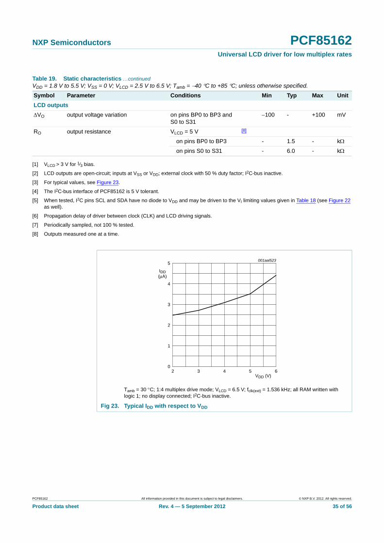
LCD outputs
VO output voltage variation on pins BP0 to BP3 andS0 to S31
100 - +100 mV
RO output resistance VLCD = 5 V [8]
on pins BP0 to BP3 - 1.5 - k
on pins S0 to S31 - 6.0 - k
Table 19. Static characteristics …continuedVDD = 1.8 V to 5.5 V; VSS = 0 V; VLCD = 2.5 V to 6.5 V; Tamb = 40 C to +85 C; unless otherwise specified.
Symbol Parameter Conditions Min Typ Max Unit
Tamb = 30 C; 1:4 multiplex drive mode; VLCD = 6.5 V; fclk(ext) = 1.536 kHz; all RAM written with logic 1; no display connected; I2C-bus inactive.
Fig 23. Typical IDD with respect to VDD
VDD (V)2 653 4
001aal523
2
3
1
4
5
IDD(μA)
0
PCF85162 All information provided in this document is subject to legal disclaimers. © NXP B.V. 2012. All rights reserved.
Product data sheet Rev. 4 — 5 September 2012 36 of 56
NXP Semiconductors PCF85162Universal LCD driver for low multiplex rates
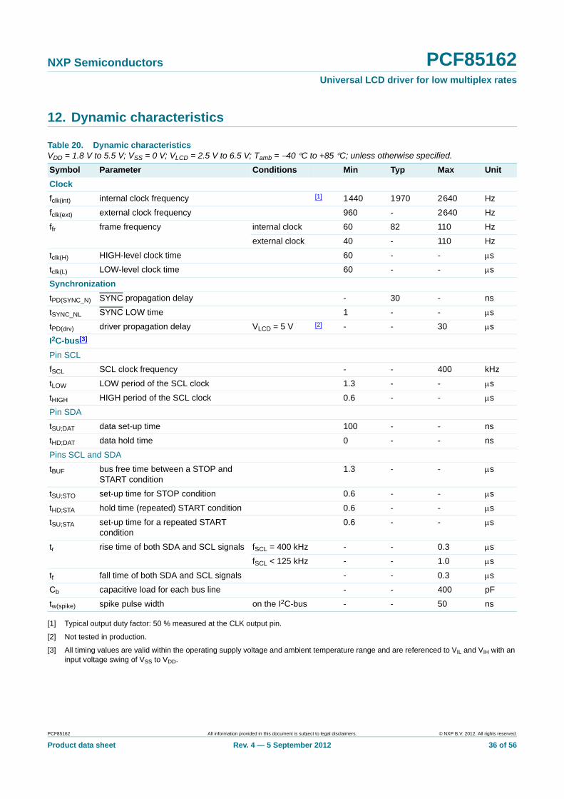
12. Dynamic characteristics
[1] Typical output duty factor: 50 % measured at the CLK output pin.
[2] Not tested in production.
[3] All timing values are valid within the operating supply voltage and ambient temperature range and are referenced to VIL and VIH with an input voltage swing of VSS to VDD.
Table 20. Dynamic characteristicsVDD = 1.8 V to 5.5 V; VSS = 0 V; VLCD = 2.5 V to 6.5 V; Tamb = 40 C to +85 C; unless otherwise specified.
Symbol Parameter Conditions Min Typ Max Unit
Clock
fclk(int) internal clock frequency [1] 1440 1970 2640 Hz
fclk(ext) external clock frequency 960 - 2640 Hz
ffr frame frequency internal clock 60 82 110 Hz
external clock 40 - 110 Hz
tclk(H) HIGH-level clock time 60 - - s
tclk(L) LOW-level clock time 60 - - s
Synchronization
tPD(SYNC_N) SYNC propagation delay - 30 - ns
tSYNC_NL SYNC LOW time 1 - - s
tPD(drv) driver propagation delay VLCD = 5 V [2] - - 30 s
I2C-bus[3]
Pin SCL
fSCL SCL clock frequency - - 400 kHz
tLOW LOW period of the SCL clock 1.3 - - s
tHIGH HIGH period of the SCL clock 0.6 - - s
Pin SDA
tSU;DAT data set-up time 100 - - ns
tHD;DAT data hold time 0 - - ns
Pins SCL and SDA
tBUF bus free time between a STOP and START condition
1.3 - - s
tSU;STO set-up time for STOP condition 0.6 - - s
tHD;STA hold time (repeated) START condition 0.6 - - s
tSU;STA set-up time for a repeated START condition
0.6 - - s
tr rise time of both SDA and SCL signals fSCL = 400 kHz - - 0.3 s
fSCL < 125 kHz - - 1.0 s
tf fall time of both SDA and SCL signals - - 0.3 s
Cb capacitive load for each bus line - - 400 pF
tw(spike) spike pulse width on the I2C-bus - - 50 ns
PCF85162 All information provided in this document is subject to legal disclaimers. © NXP B.V. 2012. All rights reserved.
Product data sheet Rev. 4 — 5 September 2012 37 of 56
NXP Semiconductors PCF85162Universal LCD driver for low multiplex rates
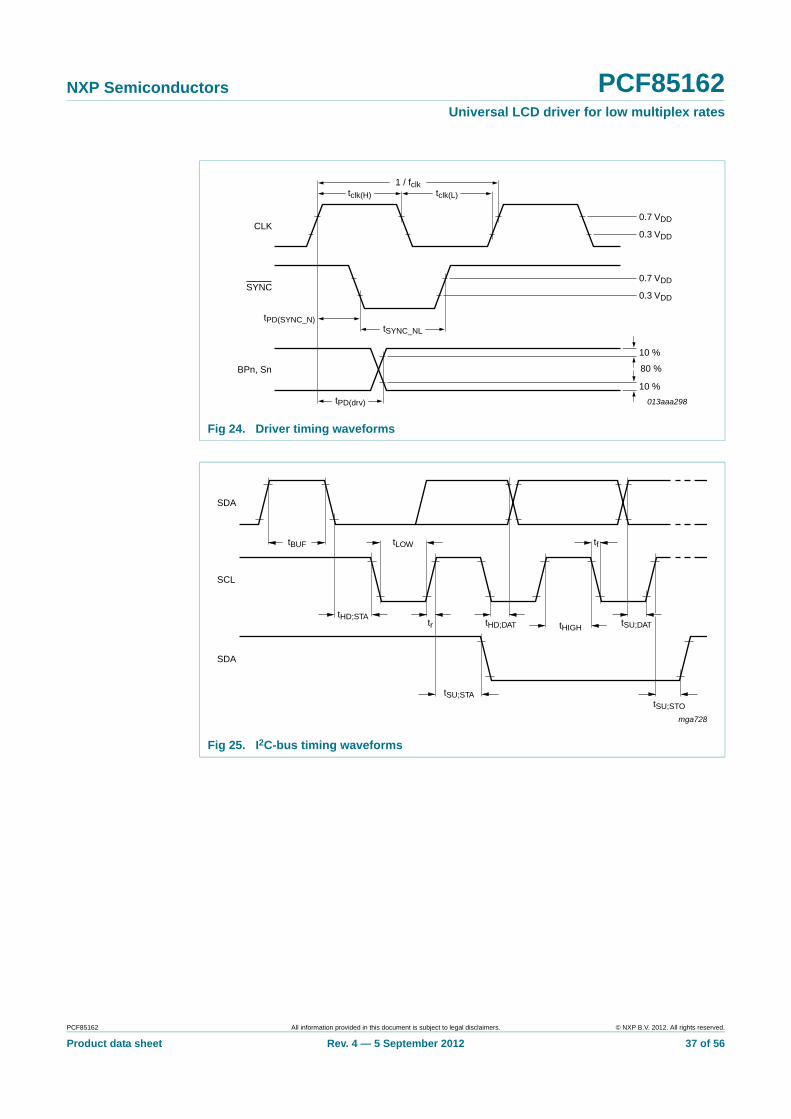
Fig 24. Driver timing waveforms
Fig 25. I2C-bus timing waveforms
013aaa298tPD(drv)
tSYNC_NL
tPD(SYNC_N)
CLK
SYNC
BPn, Sn
tclk(H) tclk(L)
1 / fclk
0.7 VDD
0.3 VDD
0.7 VDD
0.3 VDD
10 %
80 %
10 %
SDA
mga728
SDA
SCL
tSU;STAtSU;STO
tHD;STA
tBUF tLOW
tHD;DAT tHIGHtr
tf
tSU;DAT
PCF85162 All information provided in this document is subject to legal disclaimers. © NXP B.V. 2012. All rights reserved.
Product data sheet Rev. 4 — 5 September 2012 38 of 56
NXP Semiconductors PCF85162Universal LCD driver for low multiplex rates
13. Application information
13.1 Cascaded operation
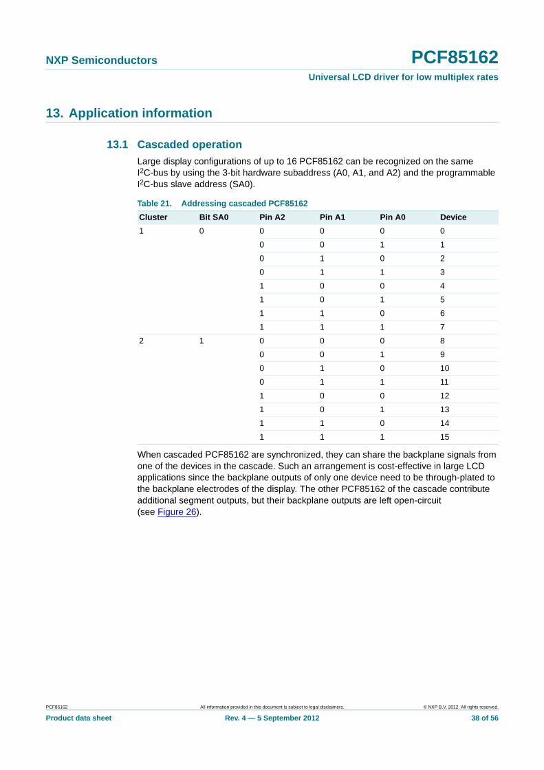
Large display configurations of up to 16 PCF85162 can be recognized on the same I2C-bus by using the 3-bit hardware subaddress (A0, A1, and A2) and the programmable I2C-bus slave address (SA0).
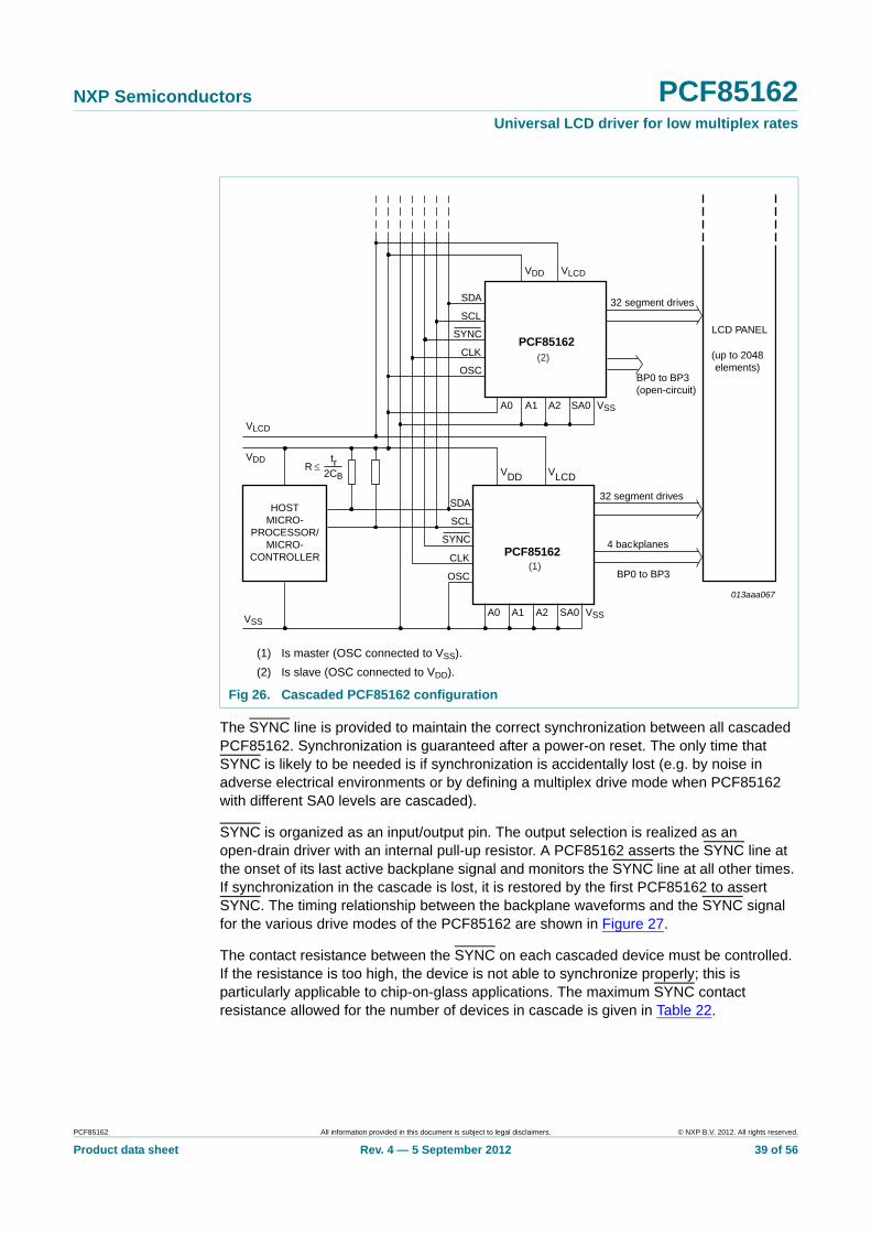
When cascaded PCF85162 are synchronized, they can share the backplane signals from one of the devices in the cascade. Such an arrangement is cost-effective in large LCD applications since the backplane outputs of only one device need to be through-plated to the backplane electrodes of the display. The other PCF85162 of the cascade contribute additional segment outputs, but their backplane outputs are left open-circuit (see Figure 26).
Table 21. Addressing cascaded PCF85162
Cluster Bit SA0 Pin A2 Pin A1 Pin A0 Device
1 0 0 0 0 0
0 0 1 1
0 1 0 2
0 1 1 3
1 0 0 4
1 0 1 5
1 1 0 6
1 1 1 7
2 1 0 0 0 8
0 0 1 9
0 1 0 10
0 1 1 11
1 0 0 12
1 0 1 13
1 1 0 14
1 1 1 15
PCF85162 All information provided in this document is subject to legal disclaimers. © NXP B.V. 2012. All rights reserved.
Product data sheet Rev. 4 — 5 September 2012 39 of 56
NXP Semiconductors PCF85162Universal LCD driver for low multiplex rates
The SYNC line is provided to maintain the correct synchronization between all cascaded PCF85162. Synchronization is guaranteed after a power-on reset. The only time that SYNC is likely to be needed is if synchronization is accidentally lost (e.g. by noise in adverse electrical environments or by defining a multiplex drive mode when PCF85162 with different SA0 levels are cascaded).
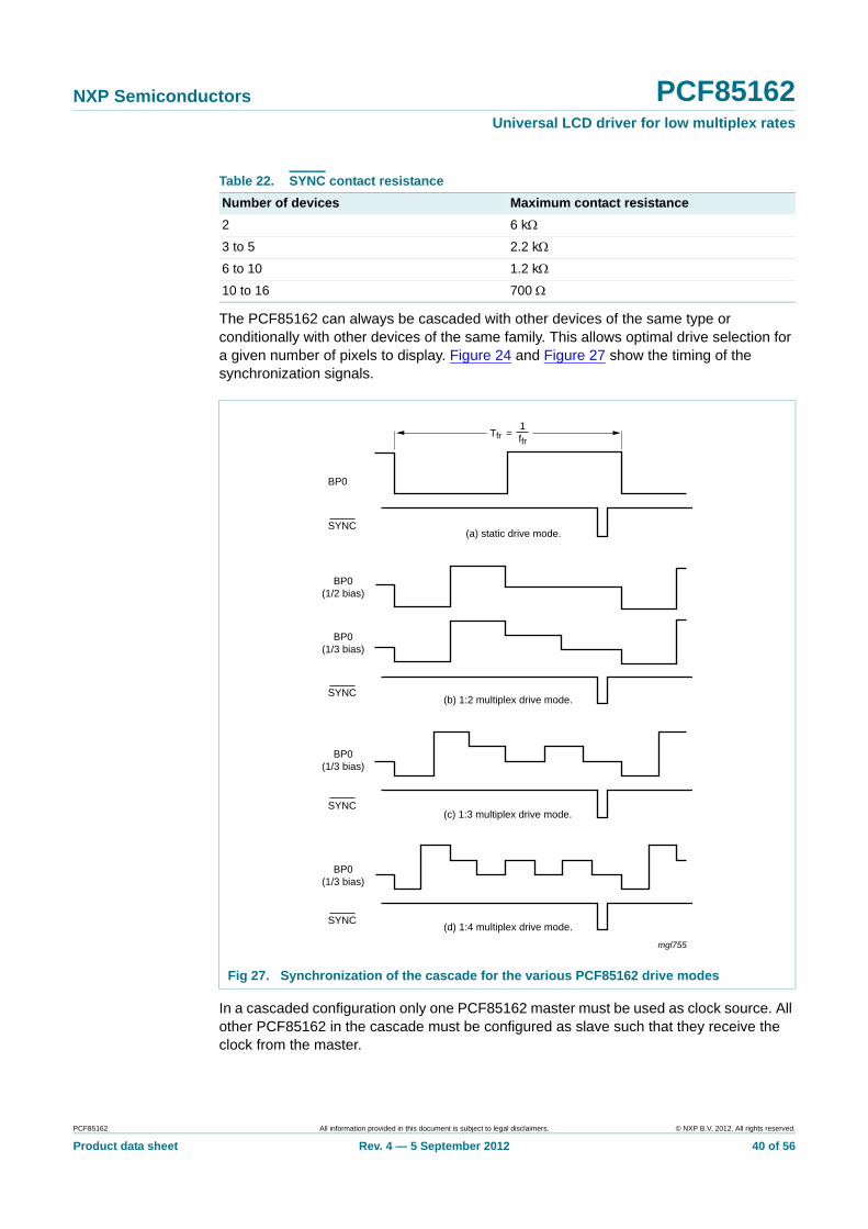
SYNC is organized as an input/output pin. The output selection is realized as an open-drain driver with an internal pull-up resistor. A PCF85162 asserts the SYNC line at the onset of its last active backplane signal and monitors the SYNC line at all other times. If synchronization in the cascade is lost, it is restored by the first PCF85162 to assert SYNC. The timing relationship between the backplane waveforms and the SYNC signal for the various drive modes of the PCF85162 are shown in Figure 27.
The contact resistance between the SYNC on each cascaded device must be controlled. If the resistance is too high, the device is not able to synchronize properly; this is particularly applicable to chip-on-glass applications. The maximum SYNC contact resistance allowed for the number of devices in cascade is given in Table 22.
(1) Is master (OSC connected to VSS).
(2) Is slave (OSC connected to VDD).
Fig 26. Cascaded PCF85162 configuration
HOSTMICRO-
PROCESSOR/MICRO-
CONTROLLER
SDA
SCL
CLK
OSC
SYNC
32 segment drives
4 backplanes
32 segment drives
LCD PANEL
(up to 2048elements)
PCF85162
A0 A1 A2 SA0
VDD
VLCD
DDV LCDV
013aaa067
SDA
SCL
SYNC
CLK
OSCBP0 to BP3 (open-circuit)
A0 A1 A2 SA0 VSS
VSSVSS
VDD VLCD
PCF85162
BP0 to BP3
Rtr
2CB≤
(2)
(1)
PCF85162 All information provided in this document is subject to legal disclaimers. © NXP B.V. 2012. All rights reserved.
Product data sheet Rev. 4 — 5 September 2012 40 of 56
NXP Semiconductors PCF85162Universal LCD driver for low multiplex rates
The PCF85162 can always be cascaded with other devices of the same type or conditionally with other devices of the same family. This allows optimal drive selection for a given number of pixels to display. Figure 24 and Figure 27 show the timing of the synchronization signals.
In a cascaded configuration only one PCF85162 master must be used as clock source. All other PCF85162 in the cascade must be configured as slave such that they receive the clock from the master.
Table 22. SYNC contact resistance
Number of devices Maximum contact resistance
2 6 k
3 to 5 2.2 k
6 to 10 1.2 k
10 to 16 700
Fig 27. Synchronization of the cascade for the various PCF85162 drive modes
Tfr = ffr1
BP0
SYNC
BP0(1/2 bias)
SYNC
BP0(1/3 bias)
(a) static drive mode.
(b) 1:2 multiplex drive mode.
(c) 1:3 multiplex drive mode.
(d) 1:4 multiplex drive mode.
BP0(1/3 bias)
SYNC
SYNC
BP0(1/3 bias)
mgl755
PCF85162 All information provided in this document is subject to legal disclaimers. © NXP B.V. 2012. All rights reserved.
Product data sheet Rev. 4 — 5 September 2012 41 of 56
NXP Semiconductors PCF85162Universal LCD driver for low multiplex rates
If an external clock source is used, all PCF85162 in the cascade must be configured such as to receive the clock from that external source (pin OSC connected to VDD). Thereby it must be ensured that the clock tree is designed such that on all PCF85162 the clock propagation delay from the clock source to all PCF85162 in the cascade is as equal as possible since otherwise synchronization artefacts may occur.
In mixed cascading configurations, care has to be taken that the specifications of the individual cascaded devices are met at all times.
PCF85162 All information provided in this document is subject to legal disclaimers. © NXP B.V. 2012. All rights reserved.
Product data sheet Rev. 4 — 5 September 2012 42 of 56
NXP Semiconductors PCF85162Universal LCD driver for low multiplex rates
14. Package outline
Fig 28. Package outline SOT362-1 (TSSOP48)
UNIT A1 A2 A3 bp c D(1) E(2) e HE L Lp Q Zywv θ
REFERENCESOUTLINEVERSION
EUROPEANPROJECTION ISSUE DATE
IEC JEDEC JEITA
mm 0.150.05
0.20.1
80
o
o0.1
DIMENSIONS (mm are the original dimensions).
Notes
1. Plastic or metal protrusions of 0.15 mm maximum per side are not included.
2. Plastic interlead protrusions of 0.25 mm maximum per side are not included.
SOT362-199-12-2703-02-19
w M
θ
AA1
A2
D
Lp
Q
detail X
E
Z
e
c
L
X
(A )3
0.25
1 24
48 25
y
pin 1 index
b
H
1.050.85
0.280.17
0.20.1
12.612.4
6.26.0
0.5 1 0.258.37.9
0.500.35
0.80.4
0.080.80.4
p
E v M A
A
TSSOP48: plastic thin shrink small outline package; 48 leads; body width 6.1 mm SOT362-1
Amax.
1.2
0 2.5 5 mm
scale
MO-153
PCF85162 All information provided in this document is subject to legal disclaimers. © NXP B.V. 2012. All rights reserved.
Product data sheet Rev. 4 — 5 September 2012 43 of 56
NXP Semiconductors PCF85162Universal LCD driver for low multiplex rates
15. Handling information
All input and output pins are protected against ElectroStatic Discharge (ESD) under normal handling. When handling Metal-Oxide Semiconductor (MOS) devices ensure that all normal precautions are taken as described in JESD625-A, IEC 61340-5 or equivalent standards.
PCF85162 All information provided in this document is subject to legal disclaimers. © NXP B.V. 2012. All rights reserved.
Product data sheet Rev. 4 — 5 September 2012 44 of 56
NXP Semiconductors PCF85162Universal LCD driver for low multiplex rates
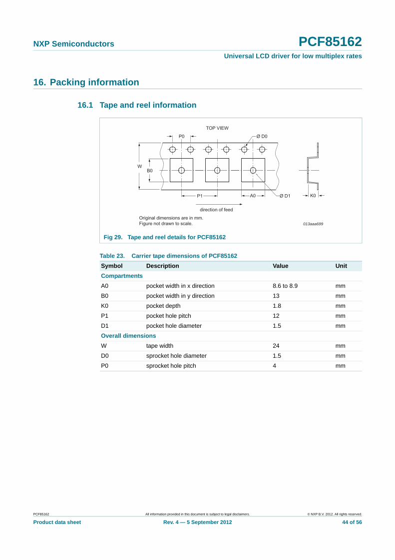
16. Packing information
16.1 Tape and reel information
Fig 29. Tape and reel details for PCF85162
Table 23. Carrier tape dimensions of PCF85162
Symbol Description Value Unit
Compartments
A0 pocket width in x direction 8.6 to 8.9 mm
B0 pocket width in y direction 13 mm
K0 pocket depth 1.8 mm
P1 pocket hole pitch 12 mm
D1 pocket hole diameter 1.5 mm
Overall dimensions
W tape width 24 mm
D0 sprocket hole diameter 1.5 mm
P0 sprocket hole pitch 4 mm
013aaa699
direction of feed
TOP VIEW
P0
A0P1
B0W
K0
Ø D0
Ø D1
Original dimensions are in mm.Figure not drawn to scale.
PCF85162 All information provided in this document is subject to legal disclaimers. © NXP B.V. 2012. All rights reserved.
Product data sheet Rev. 4 — 5 September 2012 45 of 56
NXP Semiconductors PCF85162Universal LCD driver for low multiplex rates
17. Soldering of SMD packages
This text provides a very brief insight into a complex technology. A more in-depth account of soldering ICs can be found in Application Note AN10365 “Surface mount reflow soldering description”.
17.1 Introduction to soldering
Soldering is one of the most common methods through which packages are attached to Printed Circuit Boards (PCBs), to form electrical circuits. The soldered joint provides both the mechanical and the electrical connection. There is no single soldering method that is ideal for all IC packages. Wave soldering is often preferred when through-hole and Surface Mount Devices (SMDs) are mixed on one printed wiring board; however, it is not suitable for fine pitch SMDs. Reflow soldering is ideal for the small pitches and high densities that come with increased miniaturization.
17.2 Wave and reflow soldering
Wave soldering is a joining technology in which the joints are made by solder coming from a standing wave of liquid solder. The wave soldering process is suitable for the following:
• Through-hole components
• Leaded or leadless SMDs, which are glued to the surface of the printed circuit board
Not all SMDs can be wave soldered. Packages with solder balls, and some leadless packages which have solder lands underneath the body, cannot be wave soldered. Also, leaded SMDs with leads having a pitch smaller than ~0.6 mm cannot be wave soldered, due to an increased probability of bridging.
The reflow soldering process involves applying solder paste to a board, followed by component placement and exposure to a temperature profile. Leaded packages, packages with solder balls, and leadless packages are all reflow solderable.
Key characteristics in both wave and reflow soldering are:
• Board specifications, including the board finish, solder masks and vias
• Package footprints, including solder thieves and orientation
• The moisture sensitivity level of the packages
• Package placement
• Inspection and repair
• Lead-free soldering versus SnPb soldering
17.3 Wave soldering
Key characteristics in wave soldering are:
• Process issues, such as application of adhesive and flux, clinching of leads, board transport, the solder wave parameters, and the time during which components are exposed to the wave
• Solder bath specifications, including temperature and impurities
PCF85162 All information provided in this document is subject to legal disclaimers. © NXP B.V. 2012. All rights reserved.
Product data sheet Rev. 4 — 5 September 2012 46 of 56
NXP Semiconductors PCF85162Universal LCD driver for low multiplex rates
17.4 Reflow soldering
Key characteristics in reflow soldering are:
• Lead-free versus SnPb soldering; note that a lead-free reflow process usually leads to higher minimum peak temperatures (see Figure 30) than a SnPb process, thus reducing the process window
• Solder paste printing issues including smearing, release, and adjusting the process window for a mix of large and small components on one board
• Reflow temperature profile; this profile includes preheat, reflow (in which the board is heated to the peak temperature) and cooling down. It is imperative that the peak temperature is high enough for the solder to make reliable solder joints (a solder paste characteristic). In addition, the peak temperature must be low enough that the packages and/or boards are not damaged. The peak temperature of the package depends on package thickness and volume and is classified in accordance with Table 24 and 25
Moisture sensitivity precautions, as indicated on the packing, must be respected at all times.
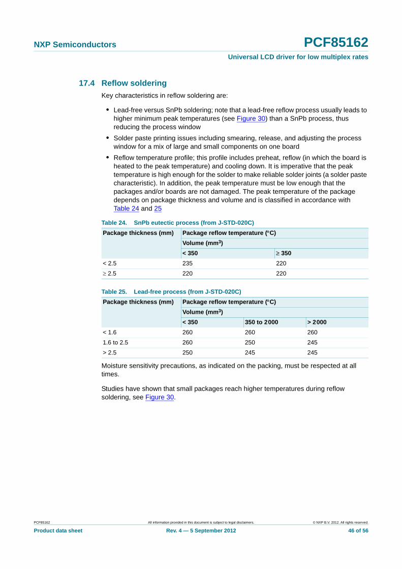
Studies have shown that small packages reach higher temperatures during reflow soldering, see Figure 30.
Table 24. SnPb eutectic process (from J-STD-020C)
Package thickness (mm) Package reflow temperature (C)
Volume (mm3)
< 350 350
< 2.5 235 220
2.5 220 220
Table 25. Lead-free process (from J-STD-020C)
Package thickness (mm) Package reflow temperature (C)
Volume (mm3)
< 350 350 to 2000 > 2000
< 1.6 260 260 260
1.6 to 2.5 260 250 245
> 2.5 250 245 245
PCF85162 All information provided in this document is subject to legal disclaimers. © NXP B.V. 2012. All rights reserved.
Product data sheet Rev. 4 — 5 September 2012 47 of 56
NXP Semiconductors PCF85162Universal LCD driver for low multiplex rates
For further information on temperature profiles, refer to Application Note AN10365 “Surface mount reflow soldering description”.
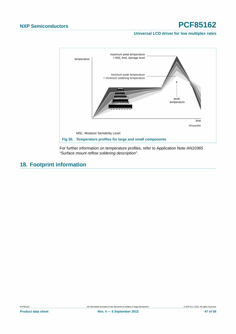
18. Footprint information
MSL: Moisture Sensitivity Level
Fig 30. Temperature profiles for large and small components
001aac844
temperature
time
minimum peak temperature= minimum soldering temperature
maximum peak temperature= MSL limit, damage level
peak temperature
PCF85162 All information provided in this document is subject to legal disclaimers. © NXP B.V. 2012. All rights reserved.
Product data sheet Rev. 4 — 5 September 2012 48 of 56
NXP Semiconductors PCF85162Universal LCD driver for low multiplex rates
Fig 31. Footprint information for reflow soldering of SOT362-1 (TSSOP48) of PCF85162T
DIMENSIONS in mm
Ay By D1 D2 Gy HyP1 C Gx
sot362-1_fr
Hx
SOT362-1
solder land
occupied area
Footprint information for reflow soldering of TSSOP48 package
AyByGy
C
Hy
Hx
Gx
P1
Generic footprint pattern
Refer to the package outline drawing for actual layout
P2
(0.125) (0.125)
D1D2 (4x)
P2
8.900 6.100 1.400 0.280 0.400 12.270 7.000 9.15014.1000.500 0.560
PCF85162 All information provided in this document is subject to legal disclaimers. © NXP B.V. 2012. All rights reserved.
Product data sheet Rev. 4 — 5 September 2012 49 of 56
NXP Semiconductors PCF85162Universal LCD driver for low multiplex rates
19. Abbreviations
Table 26. Abbreviations
Acronym Description
CMOS Complementary Metal-Oxide Semiconductor
CDM Charged Device Model
DC Direct Current
HBM Human Body Model
I2C Inter-Integrated Circuit
IC Integrated Circuit
LCD Liquid Crystal Display
LSB Least Significant Bit
MSB Most Significant Bit
MSL Moisture Sensitivity Level
PCB Printed-Circuit Board
POR Power-On Reset
RAM Random Access Memory
RC Resistance and Capacitance
RMS Root Mean Square
SCL Serial CLock line
SDA Serial DAta Line
SMD Surface-Mount Device
PCF85162 All information provided in this document is subject to legal disclaimers. © NXP B.V. 2012. All rights reserved.
Product data sheet Rev. 4 — 5 September 2012 50 of 56
NXP Semiconductors PCF85162Universal LCD driver for low multiplex rates
20. References
[1] AN10365 — Surface mount reflow soldering description
[2] AN10853 — ESD and EMC sensitivity of IC
[3] IEC 60134 — Rating systems for electronic tubes and valves and analogous semiconductor devices
[4] IEC 61340-5 — Protection of electronic devices from electrostatic phenomena
[5] IPC/JEDEC J-STD-020D — Moisture/Reflow Sensitivity Classification for Nonhermetic Solid State Surface Mount Devices
[6] JESD22-A114 — Electrostatic Discharge (ESD) Sensitivity Testing Human Body Model (HBM)
[7] JESD22-C101 — Field-Induced Charged-Device Model Test Method for Electrostatic-Discharge-Withstand Thresholds of Microelectronic Components
[8] JESD78 — IC Latch-Up Test
[9] JESD625-A — Requirements for Handling Electrostatic-Discharge-Sensitive (ESDS) Devices
[10] SNV-FA-01-02 — Marking Formats Integrated Circuits
[11] UM10204 — I2C-bus specification and user manual
[12] UM10569 — Store and transport requirements
PCF85162 All information provided in this document is subject to legal disclaimers. © NXP B.V. 2012. All rights reserved.
Product data sheet Rev. 4 — 5 September 2012 51 of 56
NXP Semiconductors PCF85162Universal LCD driver for low multiplex rates
21. Revision history
Table 27. Revision history
Document ID Release date Data sheet status Change notice Supersedes
PCF85162 v.4 20120905 Product data sheet - PCF85162 v.3
Modifications: • Adjusted values for IDD and IDD(LCD) in Table 19
• Added footprint information (Section 18)
• Added tape and reel information (Section 16)
• Added ordering options (Section 3.1)
• Improved description of bit E (Table 7)
• Enhanced display RAM description (Section 7.6)
• Fixed typos
PCF85162 v.3 20110616 Product data sheet - PCF85162 v.2
PCF85162 v.2 20100507 Product data sheet - PCF85162 v.1
PCF85162 v.1 20100107 Product data sheet - -
PCF85162 All information provided in this document is subject to legal disclaimers. © NXP B.V. 2012. All rights reserved.
Product data sheet Rev. 4 — 5 September 2012 52 of 56
NXP Semiconductors PCF85162Universal LCD driver for low multiplex rates
22. Legal information
22.1 Data sheet status
[1] Please consult the most recently issued document before initiating or completing a design.
[2] The term ‘short data sheet’ is explained in section “Definitions”.
[3] The product status of device(s) described in this document may have changed since this document was published and may differ in case of multiple devices. The latest product status information is available on the Internet at URL http://www.nxp.com.
22.2 Definitions
Draft — The document is a draft version only. The content is still under internal review and subject to formal approval, which may result in modifications or additions. NXP Semiconductors does not give any representations or warranties as to the accuracy or completeness of information included herein and shall have no liability for the consequences of use of such information.
Short data sheet — A short data sheet is an extract from a full data sheet with the same product type number(s) and title. A short data sheet is intended for quick reference only and should not be relied upon to contain detailed and full information. For detailed and full information see the relevant full data sheet, which is available on request via the local NXP Semiconductors sales office. In case of any inconsistency or conflict with the short data sheet, the full data sheet shall prevail.
Product specification — The information and data provided in a Product data sheet shall define the specification of the product as agreed between NXP Semiconductors and its customer, unless NXP Semiconductors and customer have explicitly agreed otherwise in writing. In no event however, shall an agreement be valid in which the NXP Semiconductors product is deemed to offer functions and qualities beyond those described in the Product data sheet.
22.3 Disclaimers
Limited warranty and liability — Information in this document is believed to be accurate and reliable. However, NXP Semiconductors does not give any representations or warranties, expressed or implied, as to the accuracy or completeness of such information and shall have no liability for the consequences of use of such information. NXP Semiconductors takes no responsibility for the content in this document if provided by an information source outside of NXP Semiconductors.
In no event shall NXP Semiconductors be liable for any indirect, incidental, punitive, special or consequential damages (including - without limitation - lost profits, lost savings, business interruption, costs related to the removal or replacement of any products or rework charges) whether or not such damages are based on tort (including negligence), warranty, breach of contract or any other legal theory.
Notwithstanding any damages that customer might incur for any reason whatsoever, NXP Semiconductors’ aggregate and cumulative liability towards customer for the products described herein shall be limited in accordance with the Terms and conditions of commercial sale of NXP Semiconductors.
Right to make changes — NXP Semiconductors reserves the right to make changes to information published in this document, including without limitation specifications and product descriptions, at any time and without notice. This document supersedes and replaces all information supplied prior to the publication hereof.
Suitability for use — NXP Semiconductors products are not designed, authorized or warranted to be suitable for use in life support, life-critical or safety-critical systems or equipment, nor in applications where failure or malfunction of an NXP Semiconductors product can reasonably be expected to result in personal injury, death or severe property or environmental damage. NXP Semiconductors and its suppliers accept no liability for inclusion and/or use of NXP Semiconductors products in such equipment or applications and therefore such inclusion and/or use is at the customer’s own risk.
Applications — Applications that are described herein for any of these products are for illustrative purposes only. NXP Semiconductors makes no representation or warranty that such applications will be suitable for the specified use without further testing or modification.
Customers are responsible for the design and operation of their applications and products using NXP Semiconductors products, and NXP Semiconductors accepts no liability for any assistance with applications or customer product design. It is customer’s sole responsibility to determine whether the NXP Semiconductors product is suitable and fit for the customer’s applications and products planned, as well as for the planned application and use of customer’s third party customer(s). Customers should provide appropriate design and operating safeguards to minimize the risks associated with their applications and products.
NXP Semiconductors does not accept any liability related to any default, damage, costs or problem which is based on any weakness or default in the customer’s applications or products, or the application or use by customer’s third party customer(s). Customer is responsible for doing all necessary testing for the customer’s applications and products using NXP Semiconductors products in order to avoid a default of the applications and the products or of the application or use by customer’s third party customer(s). NXP does not accept any liability in this respect.
Limiting values — Stress above one or more limiting values (as defined in the Absolute Maximum Ratings System of IEC 60134) will cause permanent damage to the device. Limiting values are stress ratings only and (proper) operation of the device at these or any other conditions above those given in the Recommended operating conditions section (if present) or the Characteristics sections of this document is not warranted. Constant or repeated exposure to limiting values will permanently and irreversibly affect the quality and reliability of the device.
Terms and conditions of commercial sale — NXP Semiconductors products are sold subject to the general terms and conditions of commercial sale, as published at http://www.nxp.com/profile/terms, unless otherwise agreed in a valid written individual agreement. In case an individual agreement is concluded only the terms and conditions of the respective agreement shall apply. NXP Semiconductors hereby expressly objects to applying the customer’s general terms and conditions with regard to the purchase of NXP Semiconductors products by customer.
No offer to sell or license — Nothing in this document may be interpreted or construed as an offer to sell products that is open for acceptance or the grant, conveyance or implication of any license under any copyrights, patents or other industrial or intellectual property rights.
Document status[1][2] Product status[3] Definition
Objective [short] data sheet Development This document contains data from the objective specification for product development.
Preliminary [short] data sheet Qualification This document contains data from the preliminary specification.
Product [short] data sheet Production This document contains the product specification.
PCF85162 All information provided in this document is subject to legal disclaimers. © NXP B.V. 2012. All rights reserved.
Product data sheet Rev. 4 — 5 September 2012 53 of 56
NXP Semiconductors PCF85162Universal LCD driver for low multiplex rates
Export control — This document as well as the item(s) described herein may be subject to export control regulations. Export might require a prior authorization from competent authorities.
Non-automotive qualified products — Unless this data sheet expressly states that this specific NXP Semiconductors product is automotive qualified, the product is not suitable for automotive use. It is neither qualified nor tested in accordance with automotive testing or application requirements. NXP Semiconductors accepts no liability for inclusion and/or use of non-automotive qualified products in automotive equipment or applications.
In the event that customer uses the product for design-in and use in automotive applications to automotive specifications and standards, customer (a) shall use the product without NXP Semiconductors’ warranty of the product for such automotive applications, use and specifications, and (b) whenever customer uses the product for automotive applications beyond NXP Semiconductors’ specifications such use shall be solely at customer’s
own risk, and (c) customer fully indemnifies NXP Semiconductors for any liability, damages or failed product claims resulting from customer design and use of the product for automotive applications beyond NXP Semiconductors’ standard warranty and NXP Semiconductors’ product specifications.
Translations — A non-English (translated) version of a document is for reference only. The English version shall prevail in case of any discrepancy between the translated and English versions.
22.4 TrademarksNotice: All referenced brands, product names, service names and trademarks are the property of their respective owners.
I2C-bus — logo is a trademark of NXP B.V.
23. Contact information
For more information, please visit: http://www.nxp.com
For sales office addresses, please send an email to: [email protected]
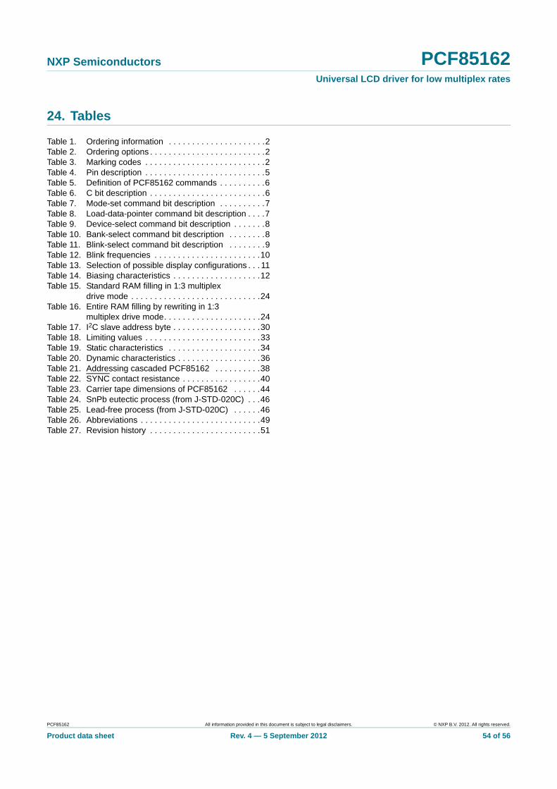
PCF85162 All information provided in this document is subject to legal disclaimers. © NXP B.V. 2012. All rights reserved.
Product data sheet Rev. 4 — 5 September 2012 54 of 56
NXP Semiconductors PCF85162Universal LCD driver for low multiplex rates
24. Tables
Table 1. Ordering information . . . . . . . . . . . . . . . . . . . . .2Table 2. Ordering options . . . . . . . . . . . . . . . . . . . . . . . . .2Table 3. Marking codes . . . . . . . . . . . . . . . . . . . . . . . . . .2Table 4. Pin description . . . . . . . . . . . . . . . . . . . . . . . . . .5Table 5. Definition of PCF85162 commands . . . . . . . . . .6Table 6. C bit description . . . . . . . . . . . . . . . . . . . . . . . . .6Table 7. Mode-set command bit description . . . . . . . . . .7Table 8. Load-data-pointer command bit description . . . .7Table 9. Device-select command bit description . . . . . . .8Table 10. Bank-select command bit description . . . . . . . .8Table 11. Blink-select command bit description . . . . . . . .9Table 12. Blink frequencies . . . . . . . . . . . . . . . . . . . . . . .10Table 13. Selection of possible display configurations . . . 11Table 14. Biasing characteristics . . . . . . . . . . . . . . . . . . .12Table 15. Standard RAM filling in 1:3 multiplex
drive mode . . . . . . . . . . . . . . . . . . . . . . . . . . . .24Table 16. Entire RAM filling by rewriting in 1:3
multiplex drive mode. . . . . . . . . . . . . . . . . . . . .24Table 17. I2C slave address byte . . . . . . . . . . . . . . . . . . .30Table 18. Limiting values . . . . . . . . . . . . . . . . . . . . . . . . .33Table 19. Static characteristics . . . . . . . . . . . . . . . . . . . .34Table 20. Dynamic characteristics . . . . . . . . . . . . . . . . . .36Table 21. Addressing cascaded PCF85162 . . . . . . . . . .38Table 22. SYNC contact resistance . . . . . . . . . . . . . . . . .40Table 23. Carrier tape dimensions of PCF85162 . . . . . .44Table 24. SnPb eutectic process (from J-STD-020C) . . .46Table 25. Lead-free process (from J-STD-020C) . . . . . .46Table 26. Abbreviations . . . . . . . . . . . . . . . . . . . . . . . . . .49Table 27. Revision history . . . . . . . . . . . . . . . . . . . . . . . .51
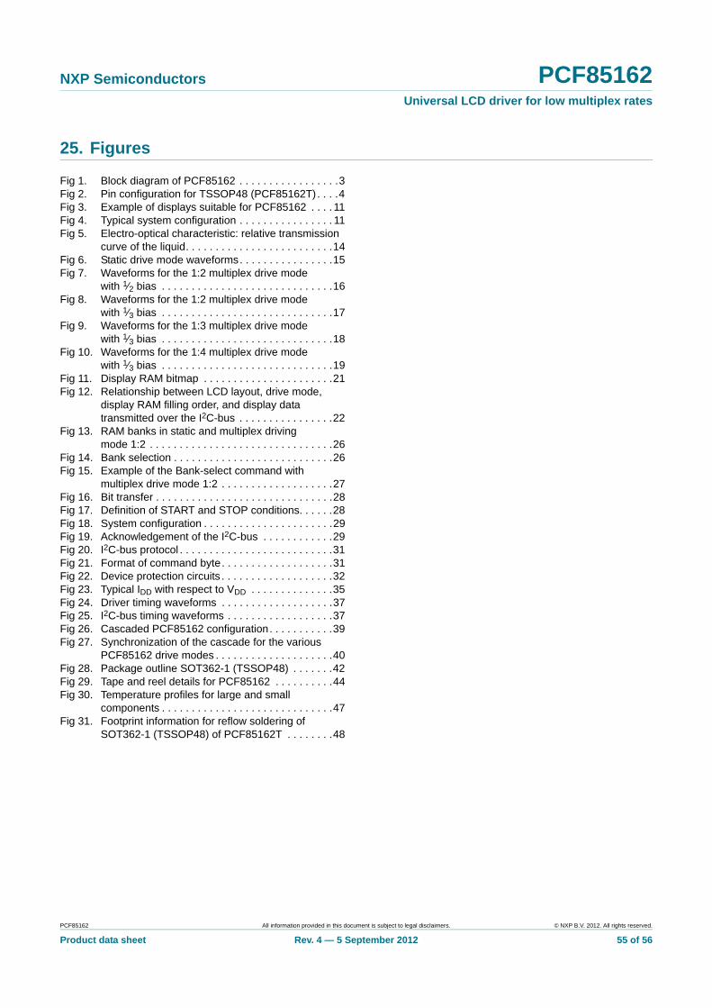
PCF85162 All information provided in this document is subject to legal disclaimers. © NXP B.V. 2012. All rights reserved.
Product data sheet Rev. 4 — 5 September 2012 55 of 56
NXP Semiconductors PCF85162Universal LCD driver for low multiplex rates
25. Figures
Fig 1. Block diagram of PCF85162 . . . . . . . . . . . . . . . . .3Fig 2. Pin configuration for TSSOP48 (PCF85162T) . . . .4Fig 3. Example of displays suitable for PCF85162 . . . . 11Fig 4. Typical system configuration . . . . . . . . . . . . . . . . 11Fig 5. Electro-optical characteristic: relative transmission
curve of the liquid. . . . . . . . . . . . . . . . . . . . . . . . .14Fig 6. Static drive mode waveforms. . . . . . . . . . . . . . . .15Fig 7. Waveforms for the 1:2 multiplex drive mode
with 1⁄2 bias . . . . . . . . . . . . . . . . . . . . . . . . . . . . .16Fig 8. Waveforms for the 1:2 multiplex drive mode
with 1⁄3 bias . . . . . . . . . . . . . . . . . . . . . . . . . . . . .17Fig 9. Waveforms for the 1:3 multiplex drive mode
with 1⁄3 bias . . . . . . . . . . . . . . . . . . . . . . . . . . . . .18Fig 10. Waveforms for the 1:4 multiplex drive mode
with 1⁄3 bias . . . . . . . . . . . . . . . . . . . . . . . . . . . . .19Fig 11. Display RAM bitmap . . . . . . . . . . . . . . . . . . . . . .21Fig 12. Relationship between LCD layout, drive mode,
display RAM filling order, and display data transmitted over the I2C-bus . . . . . . . . . . . . . . . .22
Fig 13. RAM banks in static and multiplex driving mode 1:2 . . . . . . . . . . . . . . . . . . . . . . . . . . . . . . .26
Fig 14. Bank selection . . . . . . . . . . . . . . . . . . . . . . . . . . .26Fig 15. Example of the Bank-select command with
multiplex drive mode 1:2 . . . . . . . . . . . . . . . . . . .27Fig 16. Bit transfer . . . . . . . . . . . . . . . . . . . . . . . . . . . . . .28Fig 17. Definition of START and STOP conditions. . . . . .28Fig 18. System configuration . . . . . . . . . . . . . . . . . . . . . .29Fig 19. Acknowledgement of the I2C-bus . . . . . . . . . . . .29Fig 20. I2C-bus protocol . . . . . . . . . . . . . . . . . . . . . . . . . .31Fig 21. Format of command byte. . . . . . . . . . . . . . . . . . .31Fig 22. Device protection circuits . . . . . . . . . . . . . . . . . . .32Fig 23. Typical IDD with respect to VDD . . . . . . . . . . . . . .35Fig 24. Driver timing waveforms . . . . . . . . . . . . . . . . . . .37Fig 25. I2C-bus timing waveforms . . . . . . . . . . . . . . . . . .37Fig 26. Cascaded PCF85162 configuration. . . . . . . . . . .39Fig 27. Synchronization of the cascade for the various
PCF85162 drive modes . . . . . . . . . . . . . . . . . . . .40Fig 28. Package outline SOT362-1 (TSSOP48) . . . . . . .42Fig 29. Tape and reel details for PCF85162 . . . . . . . . . .44Fig 30. Temperature profiles for large and small
components . . . . . . . . . . . . . . . . . . . . . . . . . . . . .47Fig 31. Footprint information for reflow soldering of
SOT362-1 (TSSOP48) of PCF85162T . . . . . . . .48
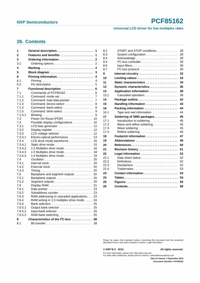
NXP Semiconductors PCF85162Universal LCD driver for low multiplex rates
© NXP B.V. 2012. All rights reserved.
For more information, please visit: http://www.nxp.comFor sales office addresses, please send an email to: [email protected]
Date of release: 5 September 2012
Document identifier: PCF85162
Please be aware that important notices concerning this document and the product(s)described herein, have been included in section ‘Legal information’.
26. Contents
1 General description . . . . . . . . . . . . . . . . . . . . . . 1
2 Features and benefits . . . . . . . . . . . . . . . . . . . . 1
3 Ordering information. . . . . . . . . . . . . . . . . . . . . 23.1 Ordering options . . . . . . . . . . . . . . . . . . . . . . . . 2
4 Marking . . . . . . . . . . . . . . . . . . . . . . . . . . . . . . . . 2
5 Block diagram . . . . . . . . . . . . . . . . . . . . . . . . . . 3
6 Pinning information. . . . . . . . . . . . . . . . . . . . . . 46.1 Pinning . . . . . . . . . . . . . . . . . . . . . . . . . . . . . . . 46.2 Pin description . . . . . . . . . . . . . . . . . . . . . . . . . 5
7 Functional description . . . . . . . . . . . . . . . . . . . 67.1 Commands of PCF85162 . . . . . . . . . . . . . . . . . 67.1.1 Command: mode-set . . . . . . . . . . . . . . . . . . . . 77.1.2 Command: load-data-pointer . . . . . . . . . . . . . . 77.1.3 Command: device-select . . . . . . . . . . . . . . . . . 87.1.4 Command: bank-select. . . . . . . . . . . . . . . . . . . 87.1.5 Command: blink-select . . . . . . . . . . . . . . . . . . . 97.1.5.1 Blinking . . . . . . . . . . . . . . . . . . . . . . . . . . . . . . . 97.2 Power-On Reset (POR) . . . . . . . . . . . . . . . . . 107.3 Possible display configurations . . . . . . . . . . . 107.3.1 LCD bias generator . . . . . . . . . . . . . . . . . . . . 127.3.2 Display register . . . . . . . . . . . . . . . . . . . . . . . . 127.3.3 LCD voltage selector . . . . . . . . . . . . . . . . . . . 127.3.3.1 Electro-optical performance . . . . . . . . . . . . . . 137.3.4 LCD drive mode waveforms . . . . . . . . . . . . . . 157.3.4.1 Static drive mode . . . . . . . . . . . . . . . . . . . . . . 157.3.4.2 1:2 Multiplex drive mode. . . . . . . . . . . . . . . . . 167.3.4.3 1:3 Multiplex drive mode. . . . . . . . . . . . . . . . . 187.3.4.4 1:4 Multiplex drive mode. . . . . . . . . . . . . . . . . 197.4 Oscillator. . . . . . . . . . . . . . . . . . . . . . . . . . . . . 207.4.1 Internal clock . . . . . . . . . . . . . . . . . . . . . . . . . 207.4.2 External clock . . . . . . . . . . . . . . . . . . . . . . . . . 207.4.3 Timing . . . . . . . . . . . . . . . . . . . . . . . . . . . . . . . 207.5 Backplane and segment outputs . . . . . . . . . . 207.5.1 Backplane outputs . . . . . . . . . . . . . . . . . . . . . 207.5.2 Segment outputs. . . . . . . . . . . . . . . . . . . . . . . 207.6 Display RAM. . . . . . . . . . . . . . . . . . . . . . . . . . 217.6.1 Data pointer . . . . . . . . . . . . . . . . . . . . . . . . . . 237.6.2 Subaddress counter . . . . . . . . . . . . . . . . . . . . 237.6.3 RAM addressing in cascaded applications. . . 237.6.4 RAM writing in 1:3 multiplex drive mode. . . . . 247.6.5 Bank selection . . . . . . . . . . . . . . . . . . . . . . . . 257.6.5.1 Output bank selector . . . . . . . . . . . . . . . . . . . 257.6.5.2 Input bank selector . . . . . . . . . . . . . . . . . . . . . 257.6.5.3 RAM bank switching . . . . . . . . . . . . . . . . . . . . 25
8 Characteristics of the I2C-bus . . . . . . . . . . . . 288.1 Bit transfer . . . . . . . . . . . . . . . . . . . . . . . . . . . 28
8.2 START and STOP conditions. . . . . . . . . . . . . 288.3 System configuration . . . . . . . . . . . . . . . . . . . 288.4 Acknowledge . . . . . . . . . . . . . . . . . . . . . . . . . 298.5 I2C-bus controller . . . . . . . . . . . . . . . . . . . . . . 308.6 Input filters . . . . . . . . . . . . . . . . . . . . . . . . . . . 308.7 I2C-bus protocol . . . . . . . . . . . . . . . . . . . . . . . 30
9 Internal circuitry . . . . . . . . . . . . . . . . . . . . . . . 32
10 Limiting values . . . . . . . . . . . . . . . . . . . . . . . . 33
11 Static characteristics . . . . . . . . . . . . . . . . . . . 34
12 Dynamic characteristics. . . . . . . . . . . . . . . . . 36
13 Application information . . . . . . . . . . . . . . . . . 3813.1 Cascaded operation. . . . . . . . . . . . . . . . . . . . 38
14 Package outline. . . . . . . . . . . . . . . . . . . . . . . . 42
15 Handling information . . . . . . . . . . . . . . . . . . . 43
16 Packing information . . . . . . . . . . . . . . . . . . . . 4416.1 Tape and reel information . . . . . . . . . . . . . . . 44
17 Soldering of SMD packages. . . . . . . . . . . . . . 4517.1 Introduction to soldering. . . . . . . . . . . . . . . . . 4517.2 Wave and reflow soldering. . . . . . . . . . . . . . . 4517.3 Wave soldering . . . . . . . . . . . . . . . . . . . . . . . 4517.4 Reflow soldering . . . . . . . . . . . . . . . . . . . . . . 46
18 Footprint information . . . . . . . . . . . . . . . . . . . 47
19 Abbreviations . . . . . . . . . . . . . . . . . . . . . . . . . 49
20 References. . . . . . . . . . . . . . . . . . . . . . . . . . . . 50
21 Revision history . . . . . . . . . . . . . . . . . . . . . . . 51
22 Legal information . . . . . . . . . . . . . . . . . . . . . . 5222.1 Data sheet status . . . . . . . . . . . . . . . . . . . . . . 5222.2 Definitions . . . . . . . . . . . . . . . . . . . . . . . . . . . 5222.3 Disclaimers . . . . . . . . . . . . . . . . . . . . . . . . . . 5222.4 Trademarks . . . . . . . . . . . . . . . . . . . . . . . . . . 53
23 Contact information . . . . . . . . . . . . . . . . . . . . 53
24 Tables . . . . . . . . . . . . . . . . . . . . . . . . . . . . . . . . 54
25 Figures . . . . . . . . . . . . . . . . . . . . . . . . . . . . . . . 55
26 Contents. . . . . . . . . . . . . . . . . . . . . . . . . . . . . . 56