Embed Size (px)
Citation preview

1
Frequency Response of Amplifier
• Input signal of an amplifier can always be expressed as the sum of sinusoidal signals.
• The amplifier performance can be characterized by its frequency response.

2
Amplifier Transmission or Transfer Function
3
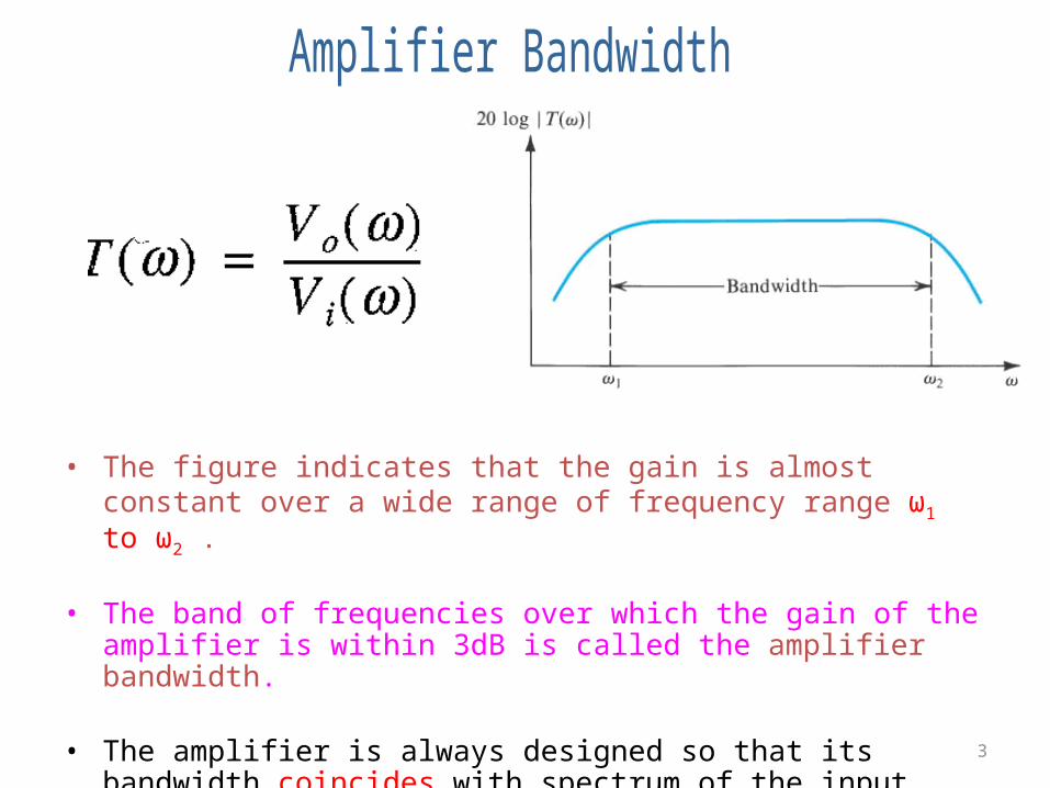
• The figure indicates that the gain is almost constant over a wide range of frequency range ω1 to ω2 .
• The band of frequencies over which the gain of the amplifier is within 3dB is called the amplifier bandwidth.
• The amplifier is always designed so that its bandwidth coincides with spectrum of the input signal (Distortion less amplification)

4
Amplifier Transfer Function• Amplifier Types
– Direct Coupled or dc amplifier– Capacitively Coupled or ac amplifier
• Difference– Gain of the ac amplifier falls off at low frequencies
• Amplifier gain is constant over a wide range of frequencies, called Mid-band
5
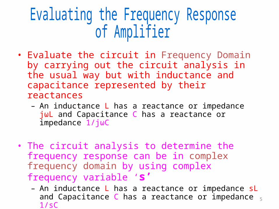
• Evaluate the circuit in Frequency Domain by carrying out the circuit analysis in the usual way but with inductance and capacitance represented by their reactances– An inductance L has a reactance or impedance jωL and Capacitance C
has a reactance or impedance 1/jωC
• The circuit analysis to determine the frequency response can be in complex frequency domain by using complex frequency variable ‘s’– An inductance L has a reactance or impedance sL and Capacitance C
has a reactance or impedance 1/sC

Frequency Response of DC Amplifier
Figure 6.12 Frequency response of a direct-coupled (dc) amplifier. Observe that the gain does not fall off at low frequencies, and the midband gain AM extends down to zero frequency.

7
A resistively loaded MOS differential pair
It is assumed that the total impedance between node S and ground is ZSS,
consisting of a resistance RSS in parallel with a capacitance CSS.
CSS includes Cbd & Cgd of QS as well as Csb1 & Csb2.
8
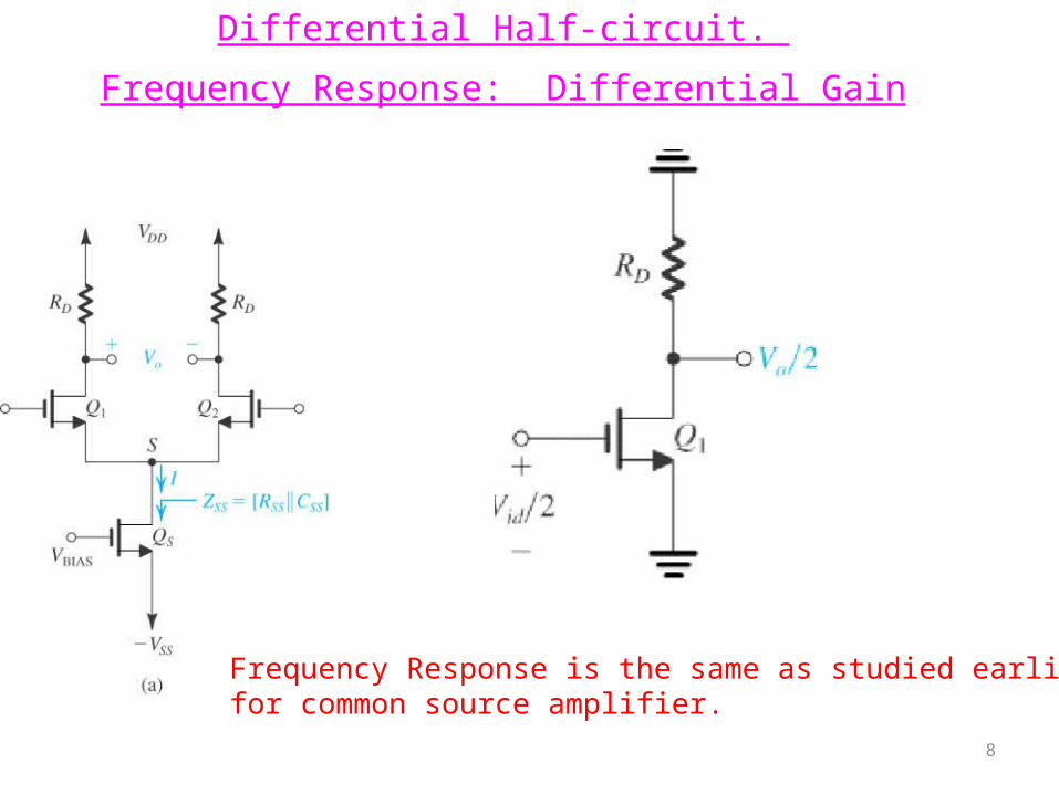
Differential Half-circuit.
Frequency Response: Differential Gain
Frequency Response is the same as studied earlier for common source amplifier.
Microelectronic Circuits - Fifth Edition Sedra/Smith
9
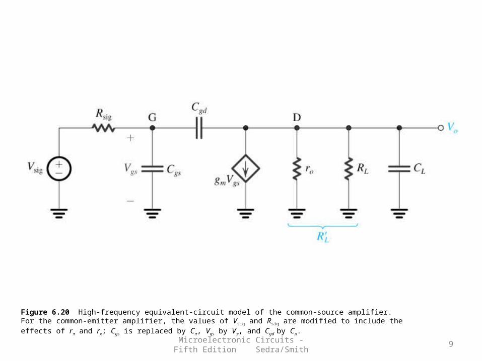
Figure 6.20 High-frequency equivalent-circuit model of the common-source amplifier. For the common-emitter amplifier, the values of Vsig and Rsig are modified to include the effects of rp and rx; Cgs is replaced by Cp, Vgs by Vp, and Cgd by Cm.

Microelectronic Circuits - Fifth Edition Sedra/Smith
10
Figure 6.23 Analysis of the CS high-frequency equivalent circuit.

Microelectronic Circuits - Fifth Edition Sedra/Smith
11
Figure 6.24 The CS circuit at s 5 sZ. The output voltage Vo 5 0, enabling us to determine sZ from a node equation at D.
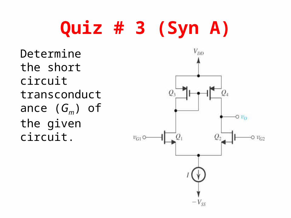
Quiz # 3 (Syn A)Determine the short circuit transconductance (Gm) of the given circuit.

Quiz # 3 (Syn B)Determine the short circuit transconductance (Gm) of the given circuit.

14
Common-mode half-circuit.

15
Common-mode half-circuit.
D
D
SS
Dcm R
R
R
RA
2
SSSSD
D
SS
D
D
D
SS
Dcm RsC
R
R
R
R
R
R
Z
RA
1
22
SSSS
SSSSSSSS RsC
RCRZ
1||
Acm has a zero on the negative real-axis of the s-plan with frequency ωz
SSSSz
SSSSz CR
fCR
2
11

16
Figure 7.37 Variation of (a) common-mode gain, (b) differential gain, and (c) common-mode rejection ratio with frequency.
SSSSSS
D
SS
Dcm RsC
R
R
Z
RA 1
22

17
Figure 7.37 Variation of (a) common-mode gain, (b) differential gain, and (c) common-mode rejection ratio with frequency.
SSSSSS
D
SS
Dcm RsC
R
R
Z
RA 1
22

18
Figure 7.38 The second stage in a differential amplifier is relied on to suppress high-frequency noise injected by the power supply of the first stage, and therefore
must maintain a high CMRR at higher frequencies.

Exercise 7.15

Microelectronic Circuits - Fifth Edition Sedra/Smith
20
Figure 6.22 Application of the open-circuit time-constants method to the CS equivalent circuit of Fig. 6.20.
21
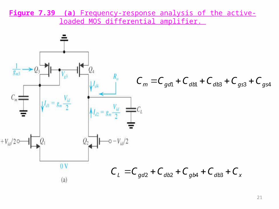
Figure 7.39 (a) Frequency-response analysis of the active-loaded MOS differential amplifier.
43311 gsgsdbdbgdm CCCCCC
xdbgbdbgdL CCCCCC 3422

22
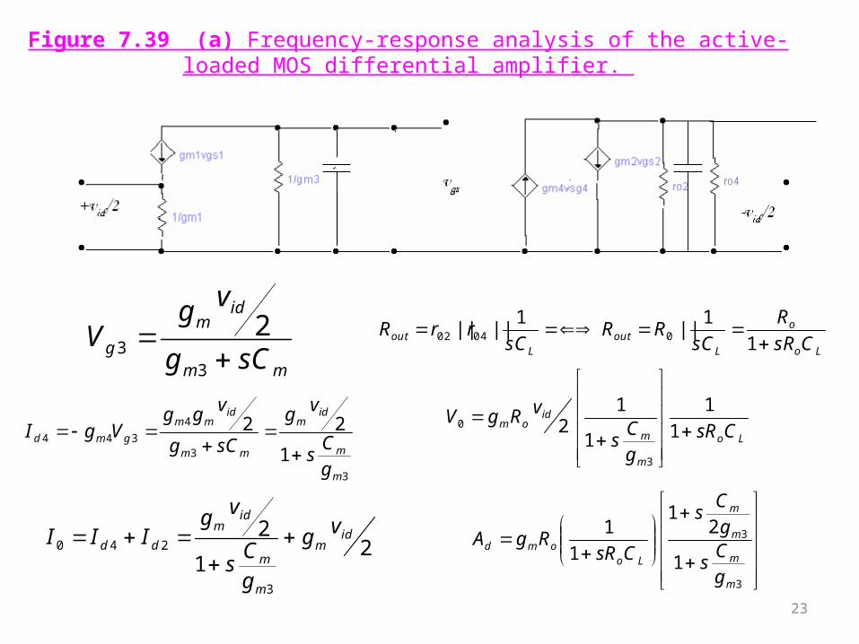
Figure 7.39 (a) Frequency-response analysis of the active-loaded MOS differential amplifier.
43311 gsgsdbdbgdm CCCCCC xdbgbdbgdL CCCCCC 3422
23
Figure 7.39 (a) Frequency-response analysis of the active-loaded MOS differential amplifier.
mm
idm
g sCg
vgV
33
2
3
3
4
344
1
22
m
m
idm
mm
idmm
gmd
gCs
vg
sCg
vggVgI
21
2
3
240id
m
m
m
idm
ddvg
gCs
vgIII
Lo
o
Lout
Lout CsR
R
sCRR
sCrrR
1
1||
1|||| 00402
Lo
m
m
idom CsR
gCs
vRgV
1
1
1
12
3
0
3
3
1
21
1
1
m
m
m
m
Loomd
gCs
gC
s
CsRRgA

25
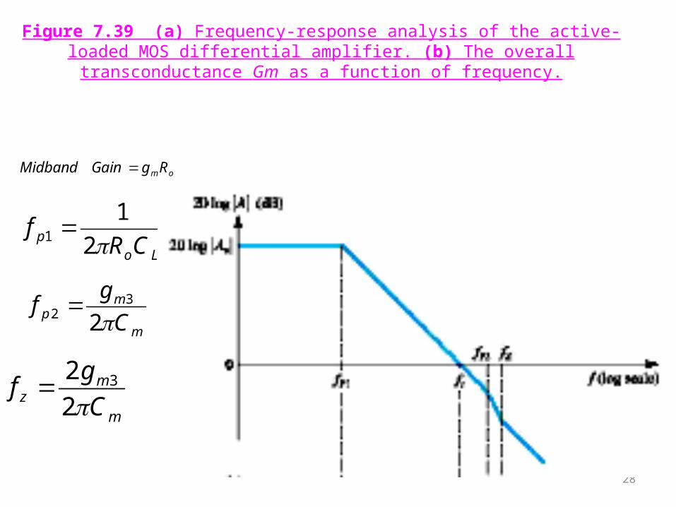
Figure 7.39 (a) Frequency-response analysis of the active-loaded MOS differential amplifier. (b) The overall transconductance Gm as a function of frequency.
xdbgbdbgdL CCCCCC 3422
0201 & rrNeglect
mm
idm
g sCg
vgV
33
2
3
3
4
344
1
22
m
m
idm
mm
idmm
gmd
gCs
vg
sCg
vggVgI
21
2
3
2440id
m
m
m
idm
ddvg
gCs
vgIII
43311 gsgsdbdbgdm CCCCCC

26
Figure 7.39 (a) Frequency-response analysis of the active-loaded MOS differential amplifier. (b) The overall transconductance Gm as a function of frequency.
Lo
o
Lout
Lout CsR
R
sCRR
sCrrR
1
1||
1|||| 00402
21
2
3
0id
m
m
m
idm vg
gCs
vgI
Lo
m
m
idom CsR
gCs
vRgV
1
1
1
12
3
0
3
3
1
21
1
1
m
m
m
m
Loomd
gCs
gC
s
CsRRgA

27
Figure 7.39 (a) Frequency-response analysis of the active-loaded MOS differential amplifier. (b) The overall transconductance Gm as a function of frequency.
3
3
1
21
1
1
m
m
m
m
Loomd
gCs
gC
s
CsRRgA
L1 C of valuelarge todue poleDominanat 2
1
Lop CRf
omRgGainMidband
m
mp C
gf
23
2
m
mz C
gf
2
2 3
The zero frequency (fz) is twice that of the pole (fp2)
28
Figure 7.39 (a) Frequency-response analysis of the active-loaded MOS differential amplifier. (b) The overall transconductance Gm as a function of frequency.
Lop CRf
2
11
omRgGainMidband
m
mp C
gf
23
2
m
mz C
gf
2
2 3

Assignment # 4
• Carry out detailed frequency response analysis of the current-mirror-loaded MOS differential pair circuit.
• Due date: 2 Dec 2011