Embed Size (px)
Citation preview

WHITE PAPER The future of atomic- level processing
HERALDHooking together European Research
in Atomic Layer Deposition
COST action MP1402
2016
1. Executive SummaryAtomic-level control of materials processing will be needed in the semiconductor industry within the next 5-10 years, and will be a powerful enabling technology for other high-tech manufacturing sectors. This will be possible if atomic-level precision can be achieved with the traditional fabrication steps – deposition, patterning and etching. There is therefore a strong need for coordinated research now into how the current concept of atomic layer deposition may be developed into selective-area patterning and atomically controlled etching.
2

3
2. Contents1. Executive summary 2
3. Introduction to current state of the art 4
4. Future market needs in atomic-level processing 5
5. Future R&D directions in atomic-level processing 6
5.1 Atomic layer etching 6
5.2 Selective area deposition or etch 9
5.3 Complementary areas for research 10
6. Benefits in multiple sectors of European industry 11
7. Acknowledgements 12
8. References 12

4
3. Introduction to current state of the artAtomic layer deposition (ALD) is a unique technique for growing ultra-thin films that is enabling new developments in high-tech manufacturing sectors such as electronics, energy and coatings. A wide range of materials can currently be deposited by ALD, including oxides, nitrides, sulfides, metals, organic and hybrid organic-inorganic materials. Unlike other chemical vapour deposition methods, ALD works by sequentially exposing a substrate to precursor gases one at a time, through rapid gas-pulsing or substrate displacement. This allows finer control of film thickness and the ability to uniformly coat all surfaces of a three-dimensional object, yielding a level of sub-nanometer precision with ALD that is unparalleled by other techniques.
ALD is now used in high-volume manufacturing. According to one of the world-leading companies in the field,1
“ALD is now firmly established as a key enabling technology. Today, ALD has become a critical technology for the manufacture of virtually all leading-edge semiconductor devices. The leading customers in our industry have already ramped several device generations based on our ALD equipment – for high-k metal gate applications in logic and foundry and for multiple patterning applications in the memory sector.”
Courtesy of Namlab.
ALD thickness control is unparalleled: <0.5 Å with uniformity <1% 1σ across 300 mm wafer8.

5
4. Future market needs in atomic-level processingThe information economy is based on continual increases in the volume, speed and energy efficiency for data transfer, processing and storage. This in turn is based on continual down-scaling of semiconductor devices (Moore’s Law) and new device concepts (Beyond Moore), both of which mean that manufacturing is becoming more challenging with every new device generation. However, to continue scaling, the semiconductor industry is facing an urgent and long-term need for improved process technologies that have the following characteristics:
u ability to add or remove material at location of choice;
u atomic-scale control of material thickness and of process drift;
u ability to coat three-dimensional (3D) structures;
u compatible with existing manufacturing process;
u can be extended to novel materials.
ALD is unique in being able to meet some of these requirements, but to fulfil all the requirements will need further R&D (section 5). If this can be achieved, these new advanced ALD-like processes will overcome the three main obstacles towards scaling that are currently being faced:
1. Achieving process tolerances at the atomic scale will allow scaling down laterally into the nanometer regime (e.g. sub-10 nm patterning);
2. Processing materials in high aspect ratio features will allow the third dimension to be exploited (e.g. gate-all-around transistor, 3D-NAND memory or 3D monolithic integration);
3. Synthesizing new materials in a fab-compatible process will open up the way to integrating new materials with higher performance.
One major reason for urgency is the delayed introduction of extreme ultra-violet (EUV) lithography in the semiconductor industry, which was originally planned for patterning at the 32 nm logic and memory nodes, but has now slipped to possible introduction at the sub-10 nm nodes. Through double-patterning, ALD can extend the use of current lithography. In addition, area-selective ALD can potentially replace some patterning steps entirely. ‘ALD-enabled patterning’ will thus likely co-exist with EUV lithography.
Atomically-precise process technologies can also be used for manufacturing in non-semiconductor sectors, enabling new functionality in a variety of mass-produced items. As a low temperature process, ALD is ideally suited for coating plastics, fabrics or fragile items. In addition, even nanometer-thin ALD layers can give sensitive substrates superior protection from moisture and oxygen. Because of this, sectors with particularly strong needs for atomic-level processing are:
u renewable energy (nanostructured fuel cells, solar cells, batteries, super-capacitors and photo-catalysts);
u medical applications (targeted/delayed drug delivery and coating implants);
u photonics (multilayer structures for lasers, lighting, plasmonics and flexible displays);
u wearable fabrics (flexible electronics, membranes or fire retardant material).
“Looking ahead to next-generation requirements, feature dimensions will soon have tolerances that are on the order of a few atoms… ALEt and ALD provide a solution by using cycles of multi-step processes that deposit or remove a few atomic layers at a time, thereby delivering precise control.” Lam Research9
“Manipulation at the molecular level promises the development of advanced tailor-made (functionalized) materials with a combination of properties that outperform existing materials.” EuMaT technology platform7
6
5. Future R&D directions in atomic-level processingAtomic layer deposition (ALD) shows promise as a platform for future atomic-level process technologies, since it is proven to already meet some of the required characteristics (thickness control, pinhole-free and 3D coating, compatible with manufacturing line). To address all of the future market needs and transform ALD into a comprehensive platform for atomic-level processing, sustained R&D will be needed. Two key areas for future research have recently been identified and are now urgently needed by front-runner companies like Intel, IBM, Lam Research and Applied Materials: (1) atomic layer etching2,3 and (2) selective area deposition.4
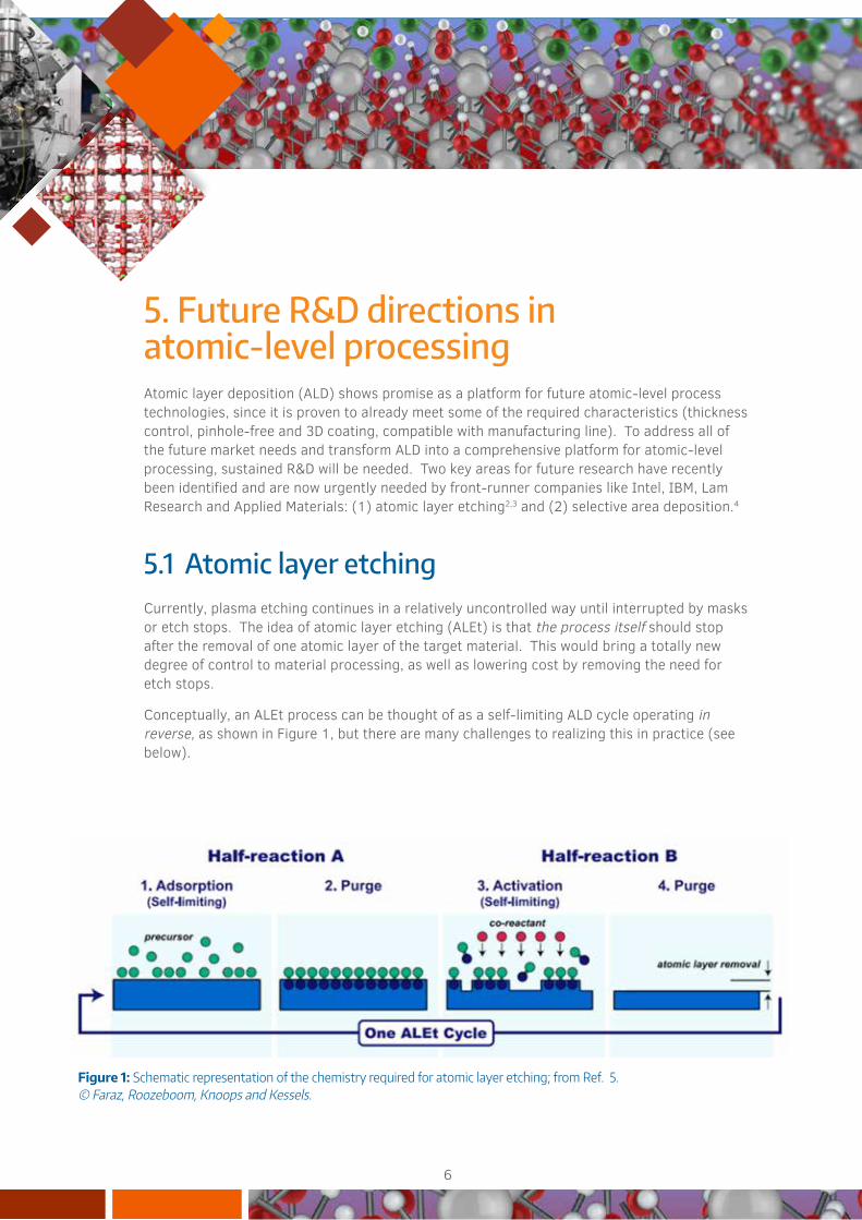
5.1 Atomic layer etchingCurrently, plasma etching continues in a relatively uncontrolled way until interrupted by masks or etch stops. The idea of atomic layer etching (ALEt) is that the process itself should stop after the removal of one atomic layer of the target material. This would bring a totally new degree of control to material processing, as well as lowering cost by removing the need for etch stops.
Conceptually, an ALEt process can be thought of as a self-limiting ALD cycle operating in reverse, as shown in Figure 1, but there are many challenges to realizing this in practice (see below).
Figure 1: Schematic representation of the chemistry required for atomic layer etching; from Ref. 5. © Faraz, Roozeboom, Knoops and Kessels.

ALD layers are both ultrathin and pinhole-free, and so are being used to protect solar cells from the air without reducing the amount of sunlight absorbed. ALD is also finding uses in other renewable energy technologies, such as super-batteries, fuel cells and photocatalysts.

8
Tailoring ALEt for different future applications:By analogy with ALD, a thermally-driven ALEt process could etch all parts of a nanostructure isotropically, even at high aspect ratios. Damage to the substrate (such as roughening) should be lower than with plasma. Controlled isotropic etching of this sort is needed to process nanowires for devices such as gate-all-around transistors and vertical NAND flash memories.
In other cases however, there are stringent temperature limits on some processes (e.g. <150°C for back-end metallization). Self-limiting plasma-based ALEt would therefore be useful for anisotropic etching at low processing temperatures. This is needed for certain nano-patterning applications (e.g. direct pattern transfer from resist).
Greater control of plasma conditions (e.g. separation of radical and ion fluxes) may allow surface reactions to be precisely controlled through the process time. Such ‘quasi-ALEt’ would enable the fabrication of self-aligned contacts.
It is proposed that cycles of ALD and ALEt can be combined so as to achieve ‘atomic scale lithography’ and thus deliver a multiple of the current lithographic resolution (e.g. double patterning).
New ALEt processes are also deemed necessary for beyond-CMOS technology nodes relying on 2D materials.
Research challenges for new ALEt process chemistry:
u Development of self-limiting etch processes for wider range of substrate materials;
u Design and synthesis of etchant chemicals for plasma and non-plasma-based ALEt that can be safely used in mass production;
u Modelling of etch chemistry and interaction of etchants and plasma with surfaces;
u Understanding the chemistry ‘rules’ that are required for AlEt.
9
Challenges in developing ALEt process equipment: u Fine control of plasma conditions, including afterglow in pulsed plasmas;
u Development of specific plasma sources (single-source or microplasma arrays);
u Roll-to-roll ALEt equipment for flexible electronics;
u Sensitive control of ion energies in etching to reduce damage;
u Advanced gas-inlet designs for very uniform and ultra-fast precursor injection;
u Measurement and control of wafer surface temperature in situ.
5.2 Selective area deposition or etchThe goal of selective area processing is to achieve different processing of different substrate materials that are adjacent to one another, despite being exposed to the same processing conditions. This would mean that a substrate would need to be patterned only once, with subsequent selective area steps propagating that pattern with fidelity.
Area-selective ALD and ALEt for various material/substrate combinations would therefore enable nanostructures of arbitrary shape and composition to be built with atomic precision. However, it is clear that developing a process for each pair of material/substrate combinations will need a tremendous experimental and modeling effort, especially in the area of novel precursor chemistries.
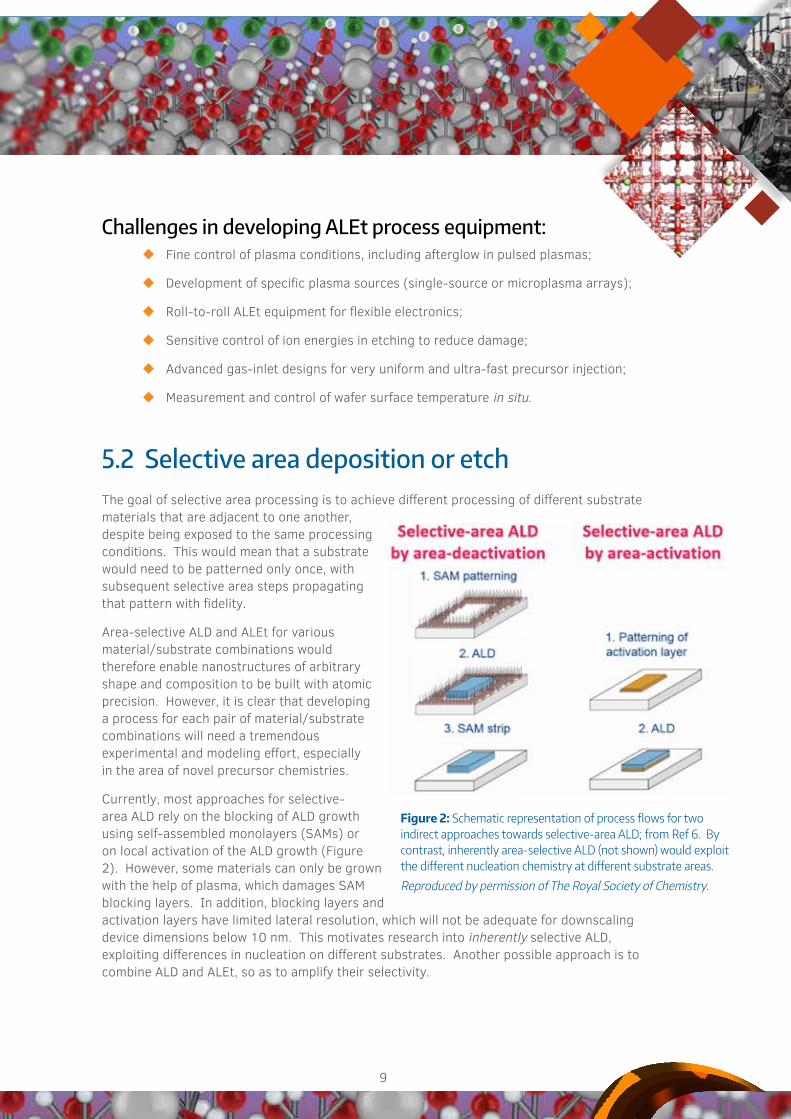
Currently, most approaches for selective-area ALD rely on the blocking of ALD growth using self-assembled monolayers (SAMs) or on local activation of the ALD growth (Figure 2). However, some materials can only be grown with the help of plasma, which damages SAM blocking layers. In addition, blocking layers and activation layers have limited lateral resolution, which will not be adequate for downscaling device dimensions below 10 nm. This motivates research into inherently selective ALD, exploiting differences in nucleation on different substrates. Another possible approach is to combine ALD and ALEt, so as to amplify their selectivity.
Figure 2: Schematic representation of process flows for two indirect approaches towards selective-area ALD; from Ref 6. By contrast, inherently area-selective ALD (not shown) would exploit the different nucleation chemistry at different substrate areas.
Reproduced by permission of The Royal Society of Chemistry.

10
Applications that will be enabled by selective-area processing:
u Fewer lithographic steps and less severe mis-alignment errors in semiconductor fabrication (see next paragraph);
u Hermetic packaging for MEMS chips;
u Cross-point memory technologies (e.g. RRAM, PCRAM, STT-MRAM).
The need for selective processes (both deposition and etch) is increasing dramatically with the transition to smaller and smaller electronic devices (e.g. logic devices shrinking from 10nm to 7 nm to 5 nm) and 3D integration (3D NAND, FinFET to 3D gate-all-around transistor). Already today, one of the main challenges of conventional lithographic patterning is to align the different layers from multiple lithographic steps. Mis-alignment errors at edges and corners are projected to be a severe limit on future downscaling. An alternative would be to use selective area ALD or ALEt to deposit or etch material only where needed on the existing pattern, removing the need for additional lithographic steps.
Key challenges for research in selective-area processing:
u Understanding how different substrates affect ALD kinetics;
u In-situ process diagnostics and characterization of nanoscale thin films;
u Understanding which surface defects affect the selectivity of the ALD growth.
u Extend selective-area ALD to a wider range of materials.
u New reagents that work at the low deposition temperatures needed for selectivity;
u How to combine the high throughput of chemical vapour deposition (CVD) with high substrate selectivity;
u Current lack of understanding of interfaces, corners and edges, which are becoming dominant in high fidelity processing at the nanoscale.
5.3 Complementary areas for researchMaterials deposited with ALD can give unique impetus to research in the broader field of advanced materials for many application sectors (not just electronics). At the same time, ALD depends on advances in fields like metrology, modelling, surface science and plasma physics. This will also be true of the emerging new fields of ALEt and selective-area processing presented here.

11
It is therefore important to develop associated areas in tandem, such as:
u Atomic-level metrology such as mass spectrometry, mass sensing and optical methods with enhanced sensitivity;
u Atomic Layer Cleaning – wet chemical processing with atomic level control and enhanced material selectivity;
u Atomic-level control in the processing of 2D materials with applications in photocatalysis, flexible electronics/displays, sensors and lightweight materials.;
u III-V semiconductor nanowire-based quantum computing.
6. Benefits in multiple sectors of European industryThe European Technology Platform for Advanced Engineering Materials and Technologies recognizes7 that processing and production technologies are the main obstacle to be overcome in realizing the commercial potential of nanotechnology in Europe:
“Today the main general challenge is to concentrate the resources to create novel production processes as a part of a complete value chain of product.”
The atomic-level processing R&D goals proposed here are concrete examples of the 3-5 year and 5-10 year objectives outlined by EuMaT relating to nanomaterials. To date, many breakthroughs in ALD processing have been successfully transferred from academic labs to high-volume manufacturing, often because of the strong commitment of companies in this field to collaborative R&D.
Atomic-level processing will be a multi-disciplinary effort encompassing chemical synthesis, surface and vacuum science, materials characterization, process engineering and application fields such as electronic engineering or renewable energy. Progress will therefore only be possible through a properly integrated R&D effort across the full supply chain. This will be true both in laboratory research (low technology readiness level, TRL) and when moving to commercialization (high TRL), as illustrated in Figure 3.
Figure 3: Simplified supply chain for materials processing at both lab scale (green) and industrial scale (blue). Not shown are the many other supply chains that feed into each segment: for example, vacuum components are supplied to equipment manufacturers.
ALD was invented in Europe and European companies still lead the way in ALD innovation, with particular strengths in manufacturing of high-purity chemicals (at the start of the supply chain) and novel processing equipment. Many of the world’s leading component suppliers for vacuum equipment and for metrology are based in Europe and stand to benefit from the potentially expanding role for atomic-level processing. Indigenous high-tech manufacturing in Europe (at the end of the supply chain) will also profit from ALD-based improvements in production and integration of advanced materials into products. Near-term applications are already emerging in batteries, photovoltaics, display technology and medical devices, all areas where Europe can be world-leading.

12
HERALD is supported by COST (European Cooperation in Science and Technology)
www.european-ald.net
Feedback is welcome to Dr Simon Elliott, Tyndall National Institute,
[email protected] or via the HERALD website at
7. AcknowledgementsCOST Action MP1402 ‘Hooking together European research in atomic layer deposition’ (HERALD) is a network of 160 researchers from 29 European countries and 6 partner countries worldwide, including universities, research institutes, multi-national companies and SMEs.
HERALD is open to all ALD researchers from the member countries and aims to provide an open and neutral forum for collaboration and the exchange of latest research findings. Members include universities, research institutes and companies representing the complete supply chain for materials processing – precursor suppliers, equipment manufacturers (three out of the four leading companies worldwide) and high-tech manufacturing (especially in the semiconductor and renewable energy sectors). The contributions to this white paper from HERALD’s academic and industrial members are gratefully acknowledged.
HERALDHooking together European Research
in Atomic Layer Deposition
COST action MP1402
COST (European Cooperation in Science and Technology) is a pan-European intergovernmental framework. Its mission is to enable break-through scientific and technological developments leading to new concepts and products and thereby contribute to strengthening Europe’s research and innovation capacities. It allows researchers, engineers and scholars to jointly develop their own ideas and take new initiatives across all fields of science and technology, while promoting multi- and interdisciplinary approaches. COST aims at fostering a better integration of less research intensive countries to the knowledge hubs of the European Research Area. The COST Association, an international not-for-profit association under Belgian law, integrates all management, governing and administrative functions necessary for the operation of the framework. The COST Association has currently 36 member countries. www.cost.eu
COST is supported by the EU Framework Programme ‘Horizon 2020’.
8. References1. C. Del Prado, CEO, ASM International N.V.; Annual Reporting (2015), www.asm.com/Downloads/2015_Statutory_annual_report.pdf 2. ECS J. Solid State Sci. Technol., vol. 4, issue 6: focus issue on ALEt and Cleaning (2015).3. K.J. Kanarik, J. Vac. Sci. Technol. A, vol. 33, p. 020802 (2015).4. F.S.M. Hashemi et al., J. Phys. Chem. C, vol. 118, p. 10957– 10962 (2014).5. T. Faraz et al., ECS J. Solid State Sci. Technol., vol. 4, p. N5023 (2015).6. A.J.M. Mackus et al., Nanoscale, vol. 6, p. 10941 (2014).7. The European Technology Platform for Advanced Engineering Materials and Technologies (EuMaT): Strategic Research Agenda, 3rd Edition, 2015.8. K. Seshan “Handbook of Thin Film Deposition: Techniques, Processes, and Technologies”, ISBN 9781437778731 (Elsevier, 2012).9. Press release 07/07/14, Lam Research Corp. http://investor.lamresearch.com/releasedetail.cfm?releaseid=858075.
© HERALD 2016