Embed Size (px)
Citation preview

1
Design of 8-BIT ALU
SANGAM SUBHASH REDDYAHMED SYED WASIF
SADDAPALLI RUDRA ABHISHEKANURAG SINGH
Advisor: Dr. DAVID W. PARENT

2
Agenda• Abstract• Introduction
– Why– Simple Theory– Back Ground information (Lit Review)
• Summary of Results• Project (Experimental) Details• Results• Conclusions

3
IntroductionWhy this project?
ALU is the building block of several circuits.
• Challenging to design a 16 logic level design working at 5ns.
• Challenging to layout.
.

4
Abstract• Goal is to design an 8-bit ALU driving up to 20fF.• Arithmetic operations are A+B, A+B+1, A+ B',
Transfer A, Transfer B, A + 1. • Logical operations are A XOR B, A AND B, A
OR B, NOT A.• The data should be transferred at clock rates of
200 MHz , with 2ns setup and hold times.
• Maximum area is 800 µm2. ×600 µm2.

5
Functional Diagram

6
NC Verilog

7
AOI 3333 Schematic
8
AOI Technique
• Technique used for designing digital circuits more directly.
• This technique becomes specifically important when speed and power considerations are not important. Instead area and number of transistors are reduced to minimum.
9
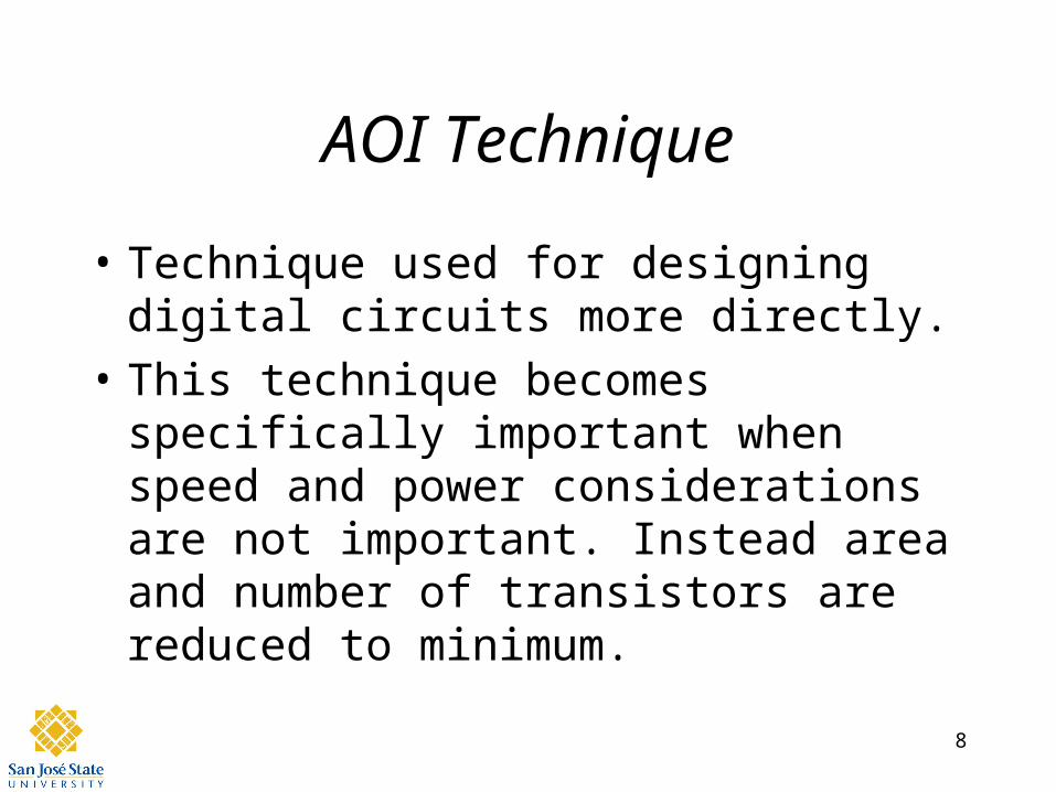
0 1 1 0 0 0 0 1 0
0 1 1 0 0 0 0 0 0
0 0 0 1 0 0 0 0 0
0 1 1 1 0 0 0 0 0
0 0 1 0 0 0 0 0 0
1 1 1 0 0 0 0 0 0
0 0 0 0 0 0 0 0 0
0 1 0 1 0 0 0 0 0
0 0 1 1 0 0 0 0 0
1 0 0 1 0 0 0 0 0
ADD
AxorB
AB
A+B
ABN
ZERO
Generate
C0 C1 C2 C3 C4 C5 C6 C7 C8
Propagate
NAND
M
MOV B
MOV A
XNOR

10

11
Carry Look Ahead Adder
• Addition of digits done parallely.
• The carry propagation time is the limiting factor in design of any adder.
• So carry propagation time has to be reduced to minimum.
• CLA is most widely used technique to reduce carry propagation time.

12
Schematic

13

14
Layout

15

16

17

18
MUX Based D Flip Flop
• Flip Flop used to store input and output bits.
• Edge triggered device meant for synchronous systems.
• Master is negative edge sensitive, Slave is positive edge sensitive.

19
Project Summary
• The Look Ahead Carry logic makes the adder faster than a conventional ripple carry adder.
• Adder design has been given due consideration because all other arithmetic functions depend on adder performance, and thus adder effects performance of entire ALU.
20
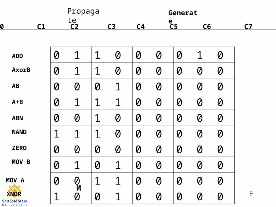
Results
• The ALU performs all 12 functions at a 200Mhz clock and a load of 30fF.
• Worst-case Power dissipation is 26.7 mW.• Area of the layout is 530×515µm2.

21
Summary
• Designed and tested almost all the design units that we learnt in the class.
• Designed an 8-Bit ALU that performs eight arithmetic and four logical functions at 200MHz frequency with setup and hold time 1ns, driving up to 30fF.
• This circuit can be used as a building block for 16/32-bit ALU.
• The Logic design can be modified to perform more functions.

22
Lessons Learned
• Got a good insight into solving LVS errors.
• Learned to take independent design decisions.
• Experience to work in a team with coordination to obtain desired results.

23
Time spent on each phase of project
• Basic logic design and verification: 3 days
• Transistor sizing: 3 days
• Layouts and Schematic: 2 weeks
• Circuit integration: 4 days
• Post Extraction Checks: 2 days

24
ACKNOWLEDGEMENTS
• Thanks to Professor David W.Parent for his guidance and timely help.
• Thanks to Cadence Design Systems for the VLSI Lab.
• Thanks to our classmates who helped us in the lab.