Embed Size (px)
Citation preview
Introduction to Microelectronics1
DIODE CIRCUITS
1 DC and low-frequency diode models
2 The diode-resistance circuit
3 Peak and power detectors
4 Rectifiers
5 Thermal sensor
Introduction to Microelectronics2
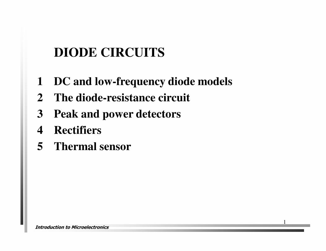
A
C
A
C
"On"
C
A
"Off"
"Short" Circuit
"Open" Circuit
+
-E
10 kΩ
VDID
+
-10 V
R
D
D
E VI
R
−=
10k Ω
10VI D =
1mAID =
Ideal diode model
Introduction to Microelectronics3
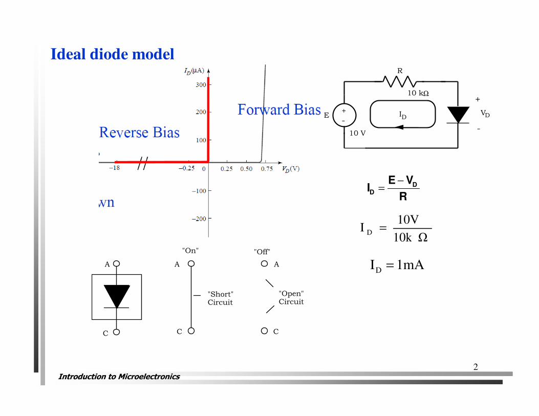
iD
iD
(a) (b)
vD Von
I = 10 – 0.6
10 k ΩI = 0.94 mA
•••• Constant-voltage-drop model Constant-voltage-drop +
resistance model
What if the input voltage is 1 V? 0.1V?
+
-10 V
10 kΩ
ID
-
(c)
V = 0.6 Von
I = ID
+
Introduction to Microelectronics
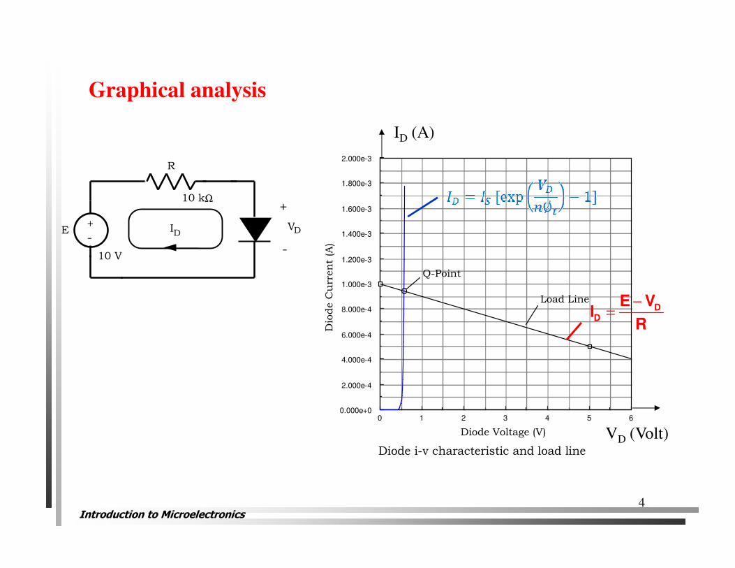
Graphical analysis
65432100.000e+0
2.000e-4
4.000e-4
6.000e-4
8.000e-4
1.000e-3
1.200e-3
1.400e-3
1.600e-3
1.800e-3
2.000e-3
Diode Voltage (V)
Dio
de C
urr
en
t (A
)
Load Line
Q-Point
Diode i-v characteristic and load line
ID (A)
VD (Volt)
D
D
E VI
R
−=
4
+
-E
10 kΩ
VDID
+
-10 V
R
Introduction to Microelectronics5
+
- R
iD
D1
v = VP
sin ω t S
0.0200.0150.0100.0050.000-15
-10
-5
0
5
10
15
Time (sec)V
olt
age (
V)
InputVoltage
OutputVoltage
InputVoltage
OutputVoltage
Half VP = 10 V and Von = 0.7 V
Simplified analysis
VS ≤ Von → Diode is ON
VS > Von → Diode is OFF
VS
VOVO = VS
Von
Half-wave rectifier circuit:
resistive load
R
V
π
1i
p
D =
R
Vi
p
Dmax =
If Vp >> Von
PIV = Vp
( average value )
Introduction to Microelectronics
6
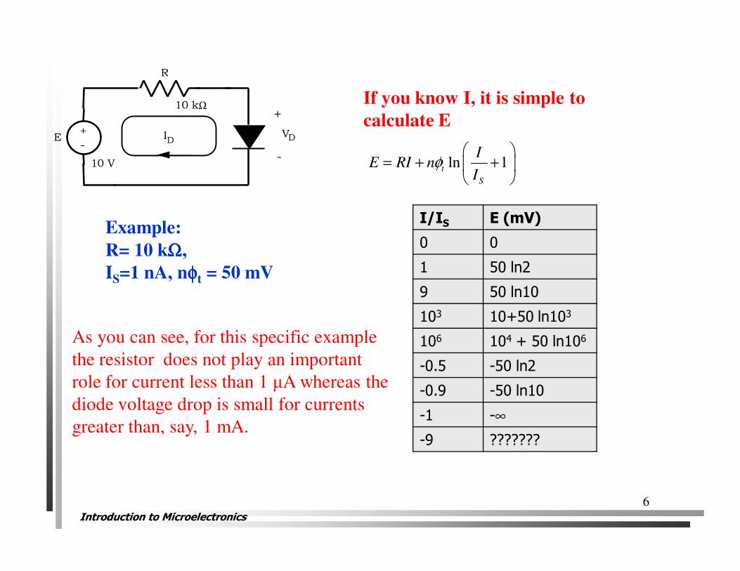
If you know I, it is simple to
calculate E
ln 1t
S
IE RI n
Iφ
= + +
I/IS E (mV)
0 0
1 50 ln2
9 50 ln10
103 10+50 ln103
106 104 + 50 ln106
-0.5 -50 ln2
-0.9 -50 ln10
-1 -∞
-9 ???????
Example:
R= 10 kΩΩΩΩ,
IS=1 nA, nφφφφt = 50 mV
As you can see, for this specific example
the resistor does not play an important
role for current less than 1 µA whereas the
diode voltage drop is small for currents
greater than, say, 1 mA.
+
-E
10 kΩ
VDID
+
-10 V
R
Introduction to Microelectronics
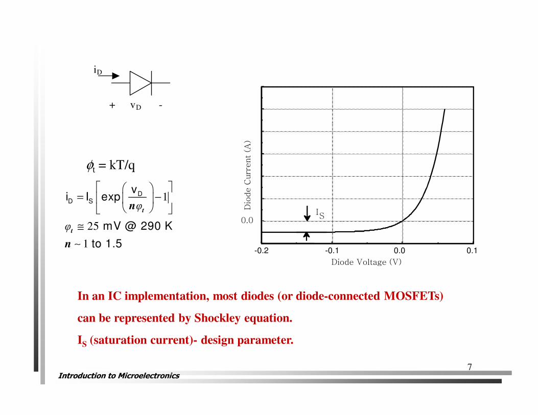
+ vD -
iD
1φ
= −
DD S
vi I exp
tn
φt = kT/q
0.10.0-0.1-0.2
0.0
Diode Voltage (V)
Dio
de C
urr
ent
(A)
IS
7
In an IC implementation, most diodes (or diode-connected MOSFETs)
can be represented by Shockley equation.
IS (saturation current)- design parameter.
25
1
mV @ 290 K
to 1.5
t
n
φ ≅
∼
Introduction to Microelectronics
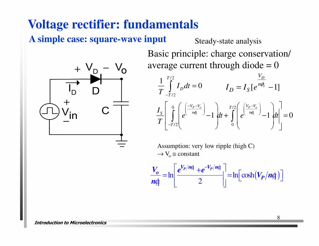
Voltage rectifier: fundamentals
Steady-state analysis
Basic principle: charge conservation/
average current through diode = 0
/ 2
/2
10
T
D
T
I dtT
−
=∫ [ 1]
D
t
V
n
D SI I e
φ= −
0 /2
/2 0
1 1 0
P o P o
t t
V V V VT
n nS
T
Ie dt e dt
T
φ φ
− − −
−
− + − =
∫ ∫
Assumption: very low ripple (high C)
→ Vo ≅ constant
( )ln ln cosh2
P t P tV n V no
P tt
V e eV n
n
− + = =
φ φ
φφ
8
A simple case: square-wave input
Introduction to Microelectronics
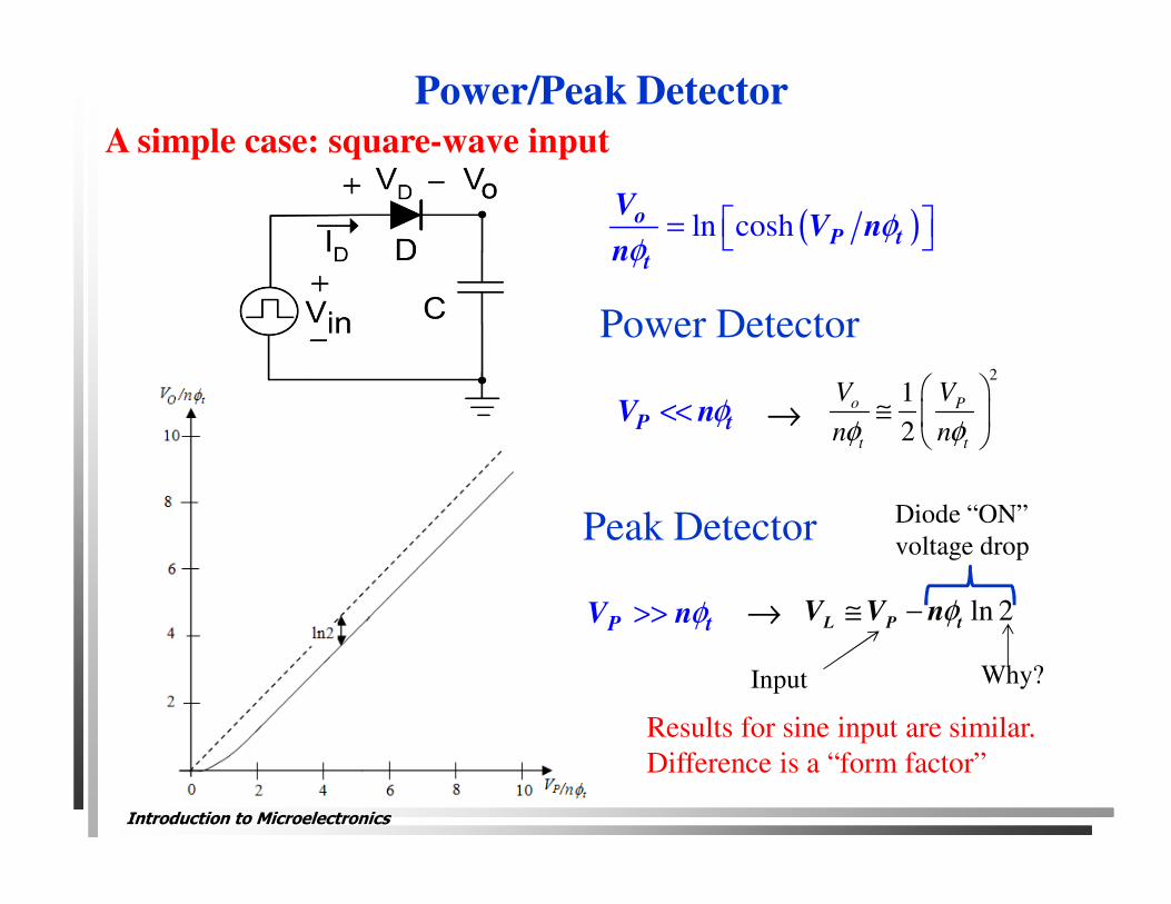
Power/Peak Detector
A simple case: square-wave input
( )ln cosh φφ
= o
P tt
VV n
n
φ<<P tV n
2
1
2
o P
t t
V V
n nφ φ
≅
→
Power Detector
Peak Detector
φ>>P tV n ln 2φ≅ −L P t
V V n→
Why?Input
Diode “ON”
voltage drop
Results for sine input are similar.
Difference is a “form factor”
Introduction to Microelectronics
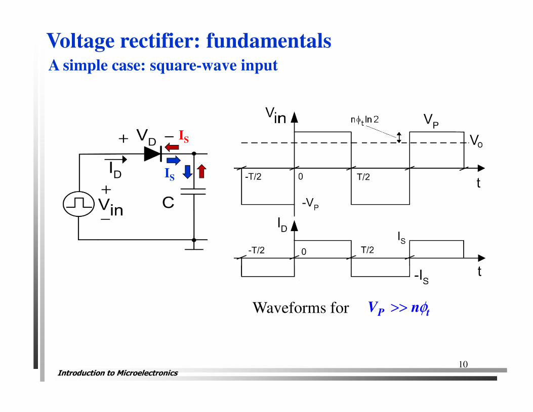
Voltage rectifier: fundamentals
10
IS
IS
A simple case: square-wave input
Waveforms for φ>>P tV n
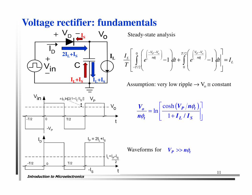
Introduction to Microelectronics11
Steady-state analysis
Waveforms for φ>>P tV n
0 /2
/2 0
1 1
P o P o
t t
V V V VT
n nS
L
T
Ie dt e dt I
T
φ φ
− − −
−
− + − =
∫ ∫
( )coshln
1 /
φ
φ
=
+
P to
t L S
V nV
n I I
Assumption: very low ripple → Vo ≅ constant
Voltage rectifier: fundamentals
IL+IS IL+IS
IS
2IL+IS IL
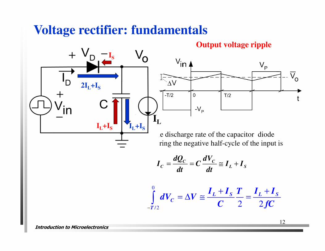
Introduction to Microelectronics12
Output voltage ripple
C C
C L S
dQ dVI C I I
dt dt= = ≅ +
The discharge rate of the capacitor diode
during the negative half-cycle of the input is
0
/22 2
L S L S
C
T
I I I ITdV V
C fC−
+ += ∆ ≅ =∫
Voltage rectifier: fundamentals
IL+IS IL+IS
IS
2IL+IS
IL
Introduction to Microelectronics
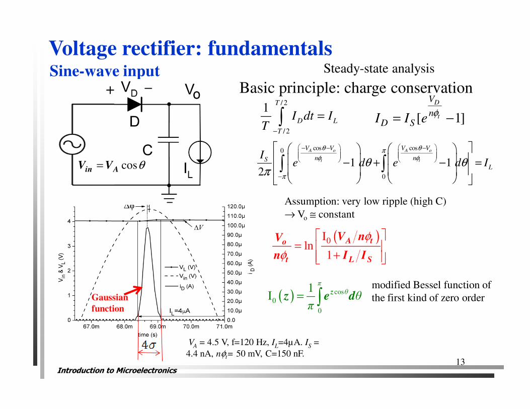
Gaussian
function
Voltage rectifier: fundamentalsSine-wave input Steady-state analysis
Basic principle: charge conservation/ 2
/2
1T
D L
T
I dt IT
−
=∫ [ 1]
D
t
V
n
D SI I e
φ= −
cos cos0
0
1 12
A o A o
t t
V V V V
n nS
L
Ie d e d I
− − −
−
− + − = ∫ ∫
θ θπφ φ
π
θ θπ
Assumption: very low ripple (high C)
→ Vo ≅ constant
13
modified Bessel function of
the first kind of zero order
( )0Iln
1
A to
t L S
V nV
n I I
=
+
φ
φ
( ) cos
0
0
1I
π
θ θπ
= ∫zz e d
cosin AV V= θ
VA
= 4.5 V, f=120 Hz, IL=4µA. I
S=
4.4 nA, nφt= 50 mV, C=150 nF.
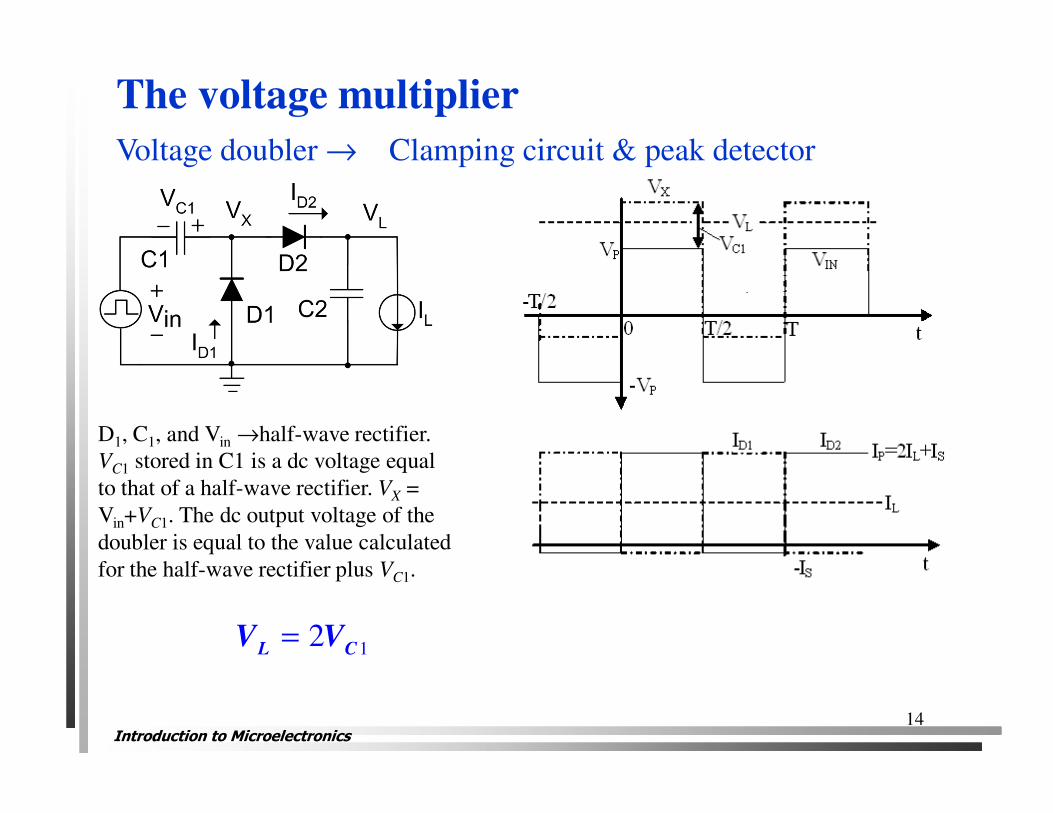
Introduction to Microelectronics14
Voltage doubler → Clamping circuit & peak detector
D1, C1, and Vin →half-wave rectifier.
VC1 stored in C1 is a dc voltage equal
to that of a half-wave rectifier. VX
=
Vin+VC1. The dc output voltage of the
doubler is equal to the value calculated
for the half-wave rectifier plus VC1.
12L CV V=
The voltage multiplier
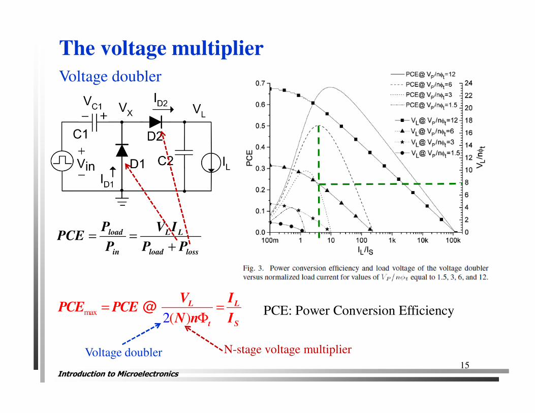
Introduction to Microelectronics15
Voltage doubler
The voltage multiplier
= =+
load L L
in load loss
P V IPCE
P P P
max)2(
@ L L
t S
V IPCE PCE
N n I= =
Φ
N-stage voltage multiplierVoltage doubler
PCE: Power Conversion Efficiency
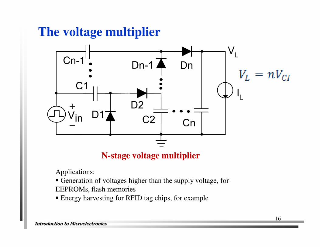
Introduction to Microelectronics16
Applications:
Generation of voltages higher than the supply voltage, for
EEPROMs, flash memories
Energy harvesting for RFID tag chips, for example
The voltage multiplier
N-stage voltage multiplier
Introduction to Microelectronics17
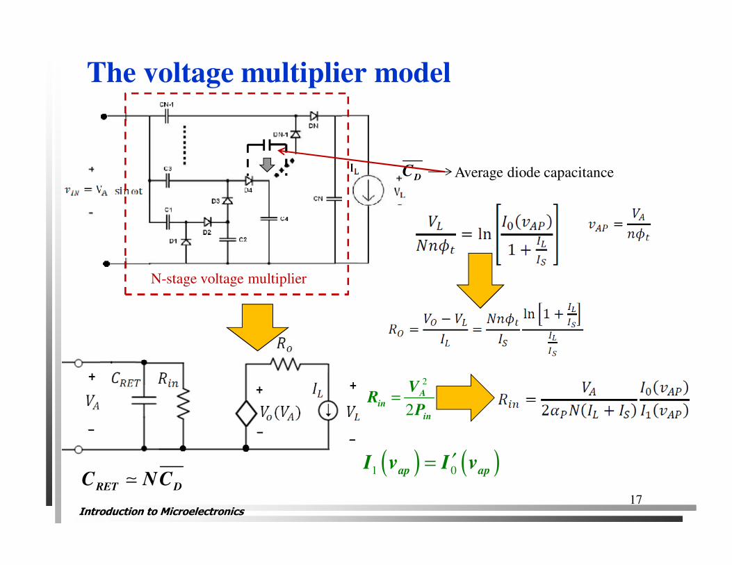
The voltage multiplier model
N-stage voltage multiplier
DC Average diode capacitance
2
2= A
in
in
VR
P
≃RET DC NC( ) ( )1 0
′=ap apI v I v
Introduction to Microelectronics
VD1 VD2
18
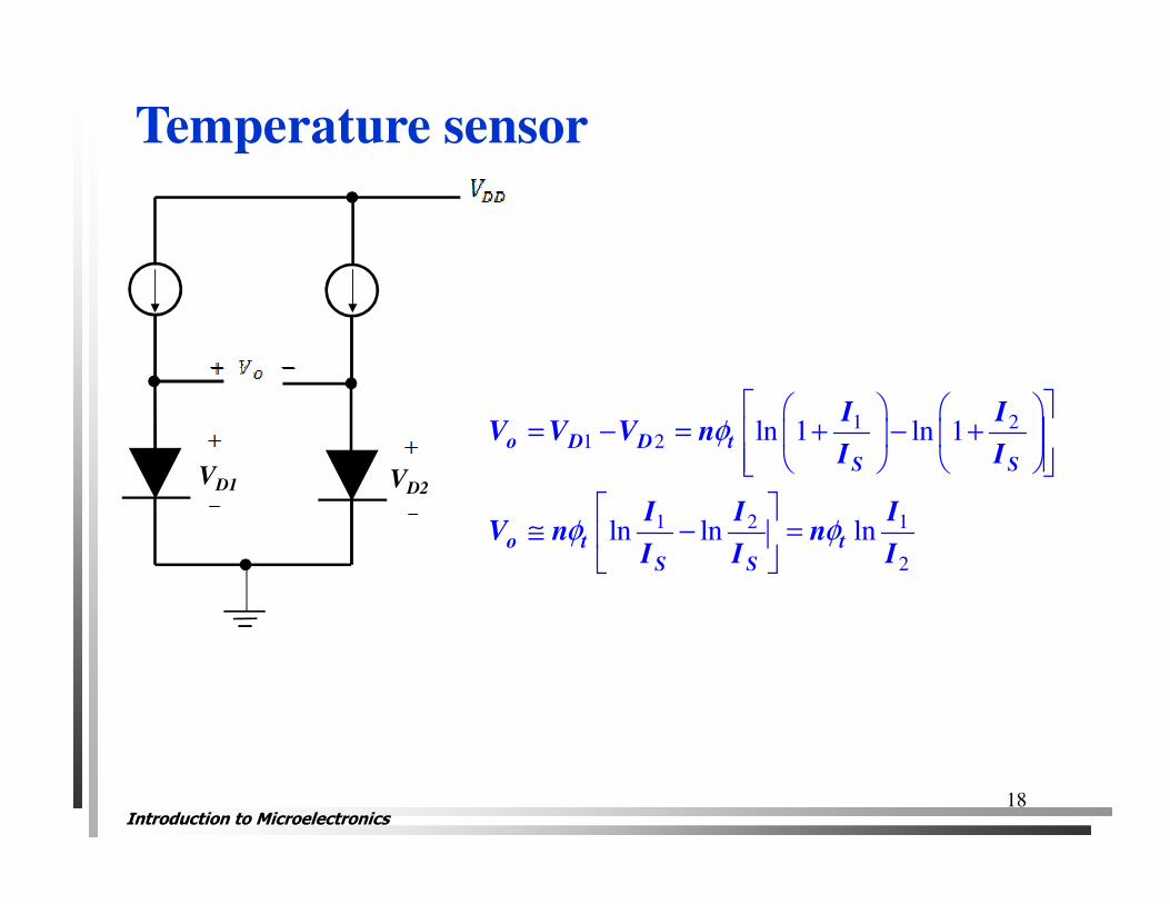
Temperature sensor
1 21 2
1 2 1
2
ln 1 ln 1
ln ln ln
o D D tS S
o t tS S
I IV V V n
I I
I I IV n n
I I I
φ
φ φ
= − = + − +
≅ − =
Introduction to Microelectronics 19
References– EEL 7061 Eletrônica Básica
http://www.lci.ufsc.br/electronics/index7061.htm
– Charles Sodini, “6.012 Microelectronic Devices and Circuits, ” OpenCourseWarehttp://ocw.mit.edu
– R. Jaeger, “Microelectronic Circuit Design,” McGraw-Hill, New York, 1997.
– A. J. Cardoso, L. G. de Carli, C. Galup-Montoro, and M. C. Schneider, “Analysis of the Rectifier Circuit Valid Down to Its Low-Voltage Limit,” IEEE Transactions on Circuits and Systems I: Regular Papers, vol. 59, no. 1, pp. 106 - 112, .–January 2012.
– A. J. Cardoso, Modelagem e projeto de conversores ac/dc de ultrabaixa tensão de operação, Tese de doutorado, UFSC, 2012
– L. G. de Carli, Modelagem e projeto de retificadores de múltiplos estágios para ultrabaixa tensão de operação, Trabalho de conclusão de curso, UFSC, 2013.
– P. Curty, N. Joehl, F. Krummenacher, C. Dehollain, and M. Declercq, “A model for u-power rectifier analysis and design,”IEEE Trans. Circuits Syst. I, Reg. Papers, vol. 52, no. 12, pp. 2771–2779, Dec. 2005.


![Active Subwoofer System SB-WA720PP - Philips d559 b0aack000004 diode [m] d560 b0aack000004 diode [m] d561 b0ba01200008 diode [m] d562 b0aack000004 diode [m] d563 b0ba01900005 diode](https://img.pdfslide.us/doc/110x75/5baed8c209d3f290738dc283/active-subwoofer-system-sb-wa720pp-philips-d559-b0aack000004-diode-m-d560-b0aack000004.jpg)


![[ifsc] retificadores](https://img.pdfslide.us/doc/110x75/56d6beb41a28ab3016933cf3/ifsc-retificadores.jpg)