Embed Size (px)
Citation preview
ISSN 0959-9428
www.rsc.org/materials Volume 21 | Number 10 | 14 March 2011 | Pages 3253–3496
FEATURE ARTICLEH. Liu et al.Chemical doping of graphene
New
Journal
ISSN 2042-6496
Food & FunctionLinking the chemistry and physics of food with health and nutrition
www.rsc.org/foodfunction Volume 1 | Number 1 | 2010 | Pages 1–100
Food & FunctionLinking the chemistry and physics of food with health and nutrition
Food science and nutrition is a highly multidisciplinary area. We know it can be difficult to keep abreast
of each other’s work, especially when there is not enough time in the day and the pile of work keeps
growing.
Wouldn’t it be great if there was a journal which pulled together high impact chemical and physical
research linking to human health and nutrition? Just one platform to find what you need in the field,
and reach exactly the right audience when you publish your work.
Food & Function provides a dedicated venue for physicists, chemists, biochemists, nutritionists and other
health scientists focusing on work related to the interaction of food components with the human body.
Go to the website now to submit your research
and register for free access!
www.rsc.org/foodfunctionRegistered Charity Number 207890
Graphene and carbon nanomaterialsGraphene and carbon nanomaterials
Dow
nloa
ded
on 3
0 A
ugus
t 201
2Pu
blis
hed
on 2
4 N
ovem
ber
2010
on
http
://pu
bs.r
sc.o
rg |
doi:1
0.10
39/C
0JM
0292
2JView Online / Journal Homepage / Table of Contents for this issue
FEATURE ARTICLE www.rsc.org/materials | Journal of Materials Chemistry
Dow
nloa
ded
on 3
0 A
ugus
t 201
2Pu
blis
hed
on 2
4 N
ovem
ber
2010
on
http
://pu
bs.r
sc.o
rg |
doi:1
0.10
39/C
0JM
0292
2J
View Online
Chemical doping of graphene
Hongtao Liu,ab Yunqi Liu*a and Daoben Zhua
Received 2nd September 2010, Accepted 14th October 2010
DOI: 10.1039/c0jm02922j
Recently, a lot of effort has been focused on improving the performance and exploring the electric
properties of graphene. This article presents a summary of chemical doping of graphene aimed at
tuning the electronic properties of graphene. p-Type and n-type doping of graphene achieved through
surface transfer doping or substitutional doping and their applications based on doping are reviewed.
Chemical doping for band gap tuning in graphene is also presented. It will be beneficial to designing
high performance electronic devices based on chemically doped graphene.
1. Introduction
Graphene, a single layer of sp2-bonded carbon atoms, has many
unique physical properties such as ambipolar electric field effect,1
high mobility of charge carriers (200,000 cm2 V�1 s�1),2,3 anom-
alous quantum Hall effect (QHE)4–6 and massless relativistic
carriers,5 all of which make graphene appropriate for many
potential applications including graphene nanoribbon (GNR)
transistors, single molecule gas detectors, supercapacitors and
transparent conducting electrodes. Moreover, field-effect tran-
sistors (FETs) based on graphene are now considered a candi-
date for post-silicon electronics.7 Modern logic circuits are based
on silicon complementary metal oxide semiconductor (CMOS)
technology. Both p-type and n-type conductions are desired to
construct complex logic circuits. Chemical doping is an effective
method to tailor the electrical properties of graphene. Although
pristine graphene exhibits ambipolar field effect, it is not air
stable and sensitive to unintentional doping by species absorbed
from the surroundings8 or residual polymers used during device
fabrication. Most graphene based transistors with ambipolar
aBeijing National Laboratory for Molecular Sciences, Key Laboratory ofOrganic Solids, Institute of Chemistry, Chinese Academy of Sciences,Beijing, 100190, P.R. China. E-mail: [email protected] University of the Chinese Academy of Sciences, Beijing, 100049,P.R. China
Hongtao Liu
Hongtao Liu was born in August
1983. He received his B.S.
degree in Applied Chemistry
from Qingdao University
(2007). Then, he joined the
Institute of Chemistry, Chinese
Academy of Sciences (CAS) as
a Ph.D. candidate. His research
interests include synthesis of
graphene derivatives and inves-
tigation of their physical prop-
erties.
This journal is ª The Royal Society of Chemistry 2011
field effect are measured in a vacuum, nitrogen or argon and/or
by annealing treatment. There is no water and other species
easily affecting the electrical properties of graphene1,9–12 under
those conditions. So, it is important to modulate the electronic
properties of graphene by controlled doping with holes or elec-
trons and reduce unnecessary contamination. This paper is
concerned with a review of experimental studies of the chemical
doping of graphene. p-Type and n-type doped graphene through
surface transfer doping and substitutional doping will be dis-
cussed, and doping for band gap tuning in graphene is also
presented. For a thorough discussion focused on synthesis,
chemistry of graphene or graphene oxide and applications, see
several excellent reviews.7,13–20
2. Mechanisms and characterization of chemicaldoping
Graphene is made out of sp2 hybrid carbon atoms with the s, px
and py atomic orbitals on each carbon atom forming three strong
s bonds with other three surrounding atoms. Overlap of the
remaining pz orbital on each carbon atom with neighboring
carbon atoms produces a filled band of p orbitals, called the
valence band and a empty band of p* orbitals known as
the conduction band. The valence and conduction bands touch at
the Brillouin zone corners thus making graphene a zero-band-
gap semiconductor.24 Fig. 1A shows the energy spectrum of
Yunqi Liu
Yunqi Liu was born on April 1,
1949. He graduated from the
Department of Chemistry,
Nanjing University in 1975, and
received a doctorate from Tokyo
Institute of Technology, Japan,
in 1991. He is currently
a professor of the Institute of
Chemistry, CAS. His research
interests include molecular
materials and devices.
J. Mater. Chem., 2011, 21, 3335–3345 | 3335
Fig. 1 (A) Left: the band structure of graphene in the honeycomb lattice.
Right: zoom-in of the energy bands close to one of the Dirac points.
Reprinted with permission from ref. 21, copyright (2009) by the Amer-
ican Physical Society. (B) Ambipolar electric field effect in single-layer
graphene. The insets show the position of the Dirac point and the Fermi
energy EF of graphene as a function of gate voltage. Reprinted with
permission from ref. 22, copyright 2007, Nature Publishing Group. (C) A
schematic diagram of the position of the Dirac point and the Fermi level
as a function of doping. The upper panel is n-type doped, pristine and p-
type doped free standing graphene (a to c). The lower panel is n-type
doped, pristine and p-type doped epitaxial graphene grown on silicon
carbide (SiC) (d to f). Reprinted with permission from ref. 23, Copyright
2008, American Chemical Society.
Dow
nloa
ded
on 3
0 A
ugus
t 201
2Pu
blis
hed
on 2
4 N
ovem
ber
2010
on
http
://pu
bs.r
sc.o
rg |
doi:1
0.10
39/C
0JM
0292
2J
View Online
graphene and zoom-in of the energy bands at one of the Dirac
point (at the K or K0 points in the Brillouin zone or the inter-
section of the valence band and the conduction band).21 Gra-
phene can be doped by electric field (Fig. 1B),22 by adsorption of
metal atoms and by substrate (Fig. 1C).23
The mechanism of chemical doping in graphene would
resemble that of carbon nanotubes, however the latter is still
controversial.25–29 From a large amount of literature, doping of
graphene may be briefly classified as electrical doping,1,30,31
achieved by changing gate voltage, and chemical doping,22,32
obtained by using chemical species. It can be seen in Fig. 1B that
pristine graphene exhibits strong ambipolar field effect indicating
the doping of electrostatic potential. Fig. 1C shows the shift of
the Dirac point relative to the Fermi level induced by chemical
doping. In this review, we focus on the chemical doping of gra-
phene. It is discussed in the following categories: surface transfer
doping and substitutional doping.14,20 For surface transfer
doping,33,34 doping is achieved by electron exchange between
a semiconductor and dopants which adsorb on the surface of
a semiconductor. Consequently, surface transfer doping is also
called adsorbate-induced doping. In general, surface transfer
doping does not disrupt the structure of graphene and most cases
of chemical doping can be reversible. However, substitutional
doping refers to the substitution of carbon atoms in the honey-
comb lattice of graphene by atoms with different number of
valence electrons such as nitrogen and boron. The incorporation
of foreign atoms would disrupt sp2 hybridization of carbon
atoms. Furthermore, substrate, residual chemical species and
ambient air can induce involuntary doping.5,35–37
Surface transfer doping occurs through charge transfer from
the adsorbed dopant (or graphene) to graphene (or
dopant).23,29,33 Charge transfer is determined by the relative
position of density of states (DOS) of the highest occupied
molecular orbital (HOMO) and lowest unoccupied molecular
orbital (LUMO) of the dopant and the Fermi level of graphene.
If the HOMO of a dopant is above the Fermi level of graphene,
charge transfers from dopant to the graphene layer, and the
dopant acts as a donor; if the LUMO is below the Fermi level of
graphene, there is a charge transfer from graphene layer to
dopant,21,38 and the dopant acts as an acceptor. Graphene can be
p-type or n-type doped via chemical doping.32,38–40 p-Type doping
drives the Dirac points of graphene above the Fermi level, and n-
type doping drives the Dirac points below the Fermi level.
Daoben Zhu
Daoben Zhu is a professor and
Director of the Organic Solids
Laboratory in the Institute of
Chemistry, CAS. He finished his
graduate courses at the East
China University of Science and
Technology in 1968. He was
selected as an academician of
CAS in 1997. His research
interests include molecular
materials and devices.
3336 | J. Mater. Chem., 2011, 21, 3335–3345
Generally speaking, molecules with electron withdrawing groups
adsorbed on the surface of graphene will lead to p-type doping of
graphene, and molecules with donating groups will lead to n-type
doping. In contrast, the mechanism of substitutional doping still
remains uncertain. p-Type doping is generally achieved by add-
ing atoms with fewer valence electrons than carbon like boron,
while n-type doping is generally achieved by adding atoms with
more valence electrons than carbon like nitrogen.
Chemical doping of graphene has so far been extensively
characterized by these three main kinds of methods: photo-
emission spectroscopy (PES), especially X-ray photoelectron
spectroscopy (XPS) and angle-resolved photoemission spec-
troscopy (ARPES), Raman spectroscopy and transport
measurement. From spectrum of XPS, we can find whether the
dopant exists by the characteristic peak of element contained in
the dopant. The doping level can be determined by areas of the
peak. The chemical states and electric states of the element could
be obtained by analyzing the high resolution spectra of the
element. ARPES is widely used to probe the electronic structure
of graphene.41–43 The band structure of graphene at Fermi level
near the K point in the Brillouin zone can be obtained from the
energy dispersions as a function of momentum along high-
symmetry directions measured by ARPES. Fermi level locates at
zero bonding energy, while the Dirac point is near, below or
This journal is ª The Royal Society of Chemistry 2011
Dow
nloa
ded
on 3
0 A
ugus
t 201
2Pu
blis
hed
on 2
4 N
ovem
ber
2010
on
http
://pu
bs.r
sc.o
rg |
doi:1
0.10
39/C
0JM
0292
2J
View Online
above the Fermi level depending on whether the graphene is
pristine or doped.
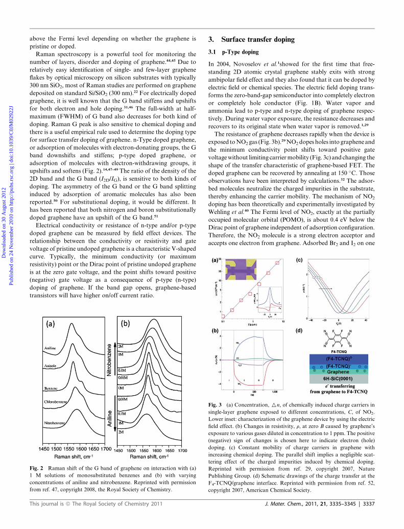
Raman spectroscopy is a powerful tool for monitoring the
number of layers, disorder and doping of graphene.44,45 Due to
relatively easy identification of single- and few-layer graphene
flakes by optical microscopy on silicon substrates with typically
300 nm SiO2, most of Raman studies are performed on graphene
deposited on standard Si/SiO2 (300 nm).22 For electrically doped
graphene, it is well known that the G band stiffens and upshifts
for both electron and hole doping.31,46 The full-width at half-
maximum (FWHM) of G band also decreases for both kind of
doping. Raman G peak is also sensitive to chemical doping and
there is a useful empirical rule used to determine the doping type
for surface transfer doping of graphene. n-Type doped graphene,
or adsorption of molecules with electron-donating groups, the G
band downshifts and stiffens; p-type doped graphene, or
adsorption of molecules with electron-withdrawing groups, it
upshifts and softens (Fig. 2).14,47–49 The ratio of the density of the
2D band and the G band (I2D/IG), is sensitive to both kinds of
doping. The asymmetry of the G band or the G band splitting
induced by adsorption of aromatic molecules has also been
reported.50 For substitutional doping, it would be different. It
has been reported that both nitrogen and boron substitutionally
doped graphene have an upshift of the G band.51
Electrical conductivity or resistance of n-type and/or p-type
doped graphene can be measured by field effect devices. The
relationship between the conductivity or resistivity and gate
voltage of pristine undoped graphene is a characteristic V-shaped
curve. Typically, the minimum conductivity (or maximum
resistivity) point or the Dirac point of pristine undoped graphene
is at the zero gate voltage, and the point shifts toward positive
(negative) gate voltage as a consequence of p-type (n-type)
doping of graphene. If the band gap opens, graphene-based
transistors will have higher on/off current ratio.
Fig. 2 Raman shift of the G band of graphene on interaction with (a)
1 M solutions of monosubstituted benzenes and (b) with varying
concentrations of aniline and nitrobenzene. Reprinted with permission
from ref. 47, copyright 2008, the Royal Society of Chemistry.
This journal is ª The Royal Society of Chemistry 2011
3. Surface transfer doping
3.1 p-Type doping
In 2004, Novoselov et al.1showed for the first time that free-
standing 2D atomic crystal graphene stably exits with strong
ambipolar field effect and they also found that it can be doped by
electric field or chemical species. The electric field doping trans-
forms the zero-band-gap semiconductor into completely electron
or completely hole conductor (Fig. 1B). Water vapor and
ammonia lead to p-type and n-type doping of graphene respec-
tively. During water vapor exposure, the resistance decreases and
recovers to its original state when water vapor is removed.1,29
The resistance of graphene decreases rapidly when the device is
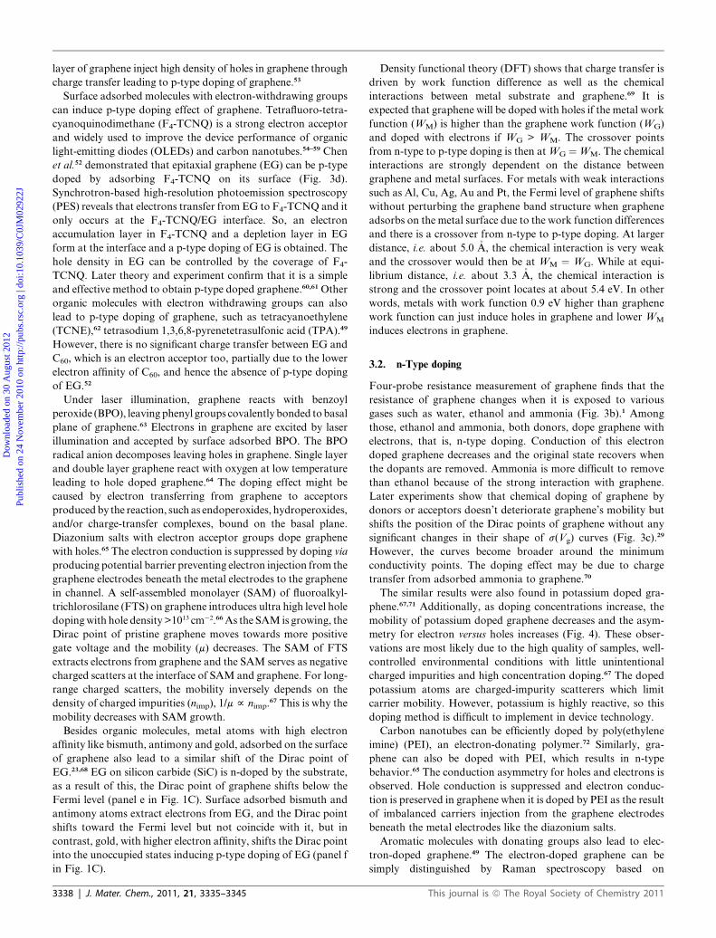
exposed to NO2 gas (Fig. 3b).29 NO2 dopes holes into graphene and
the minimum conductivity point shifts toward positive gate
voltage without limiting carrier mobility (Fig. 3c) and changing the
shape of the transfer characteristic of graphene-based FET. The
doped graphene can be recovered by annealing at 150 �C. Those
observations have been interpreted by calculations.32 The adsor-
bed molecules neutralize the charged impurities in the substrate,
thereby enhancing the carrier mobility. The mechanism of NO2
doping has been theoretically and experimentally investigated by
Wehling et al.40 The Fermi level of NO2, exactly at the partially
occupied molecular orbital (POMO), is about 0.4 eV below the
Dirac point of graphene independent of adsorption configuration.
Therefore, the NO2 molecule is a strong electron acceptor and
accepts one electron from graphene. Adsorbed Br2 and I2 on one
Fig. 3 (a) Concentration, On, of chemically induced charge carriers in
single-layer graphene exposed to different concentrations, C, of NO2.
Lower inset: characterization of the graphene device by using the electric
field effect. (b) Changes in resistivity, r, at zero B caused by graphene’s
exposure to various gases diluted in concentration to 1 ppm. The positive
(negative) sign of changes is chosen here to indicate electron (hole)
doping. (c) Constant mobility of charge carriers in graphene with
increasing chemical doping. The parallel shift implies a negligible scat-
tering effect of the charged impurities induced by chemical doping.
Reprinted with permission from ref. 29, copyright 2007, Nature
Publishing Group. (d) Schematic drawings of the charge transfer at the
F4-TCNQ/graphene interface. Reprinted with permission from ref. 52,
copyright 2007, American Chemical Society.
J. Mater. Chem., 2011, 21, 3335–3345 | 3337
Dow
nloa
ded
on 3
0 A
ugus
t 201
2Pu
blis
hed
on 2
4 N
ovem
ber
2010
on
http
://pu
bs.r
sc.o
rg |
doi:1
0.10
39/C
0JM
0292
2J
View Online
layer of graphene inject high density of holes in graphene through
charge transfer leading to p-type doping of graphene.53
Surface adsorbed molecules with electron-withdrawing groups
can induce p-type doping effect of graphene. Tetrafluoro-tetra-
cyanoquinodimethane (F4-TCNQ) is a strong electron acceptor
and widely used to improve the device performance of organic
light-emitting diodes (OLEDs) and carbon nanotubes.54–59 Chen
et al.52 demonstrated that epitaxial graphene (EG) can be p-type
doped by adsorbing F4-TCNQ on its surface (Fig. 3d).
Synchrotron-based high-resolution photoemission spectroscopy
(PES) reveals that electrons transfer from EG to F4-TCNQ and it
only occurs at the F4-TCNQ/EG interface. So, an electron
accumulation layer in F4-TCNQ and a depletion layer in EG
form at the interface and a p-type doping of EG is obtained. The
hole density in EG can be controlled by the coverage of F4-
TCNQ. Later theory and experiment confirm that it is a simple
and effective method to obtain p-type doped graphene.60,61 Other
organic molecules with electron withdrawing groups can also
lead to p-type doping of graphene, such as tetracyanoethylene
(TCNE),62 tetrasodium 1,3,6,8-pyrenetetrasulfonic acid (TPA).49
However, there is no significant charge transfer between EG and
C60, which is an electron acceptor too, partially due to the lower
electron affinity of C60, and hence the absence of p-type doping
of EG.52
Under laser illumination, graphene reacts with benzoyl
peroxide (BPO), leaving phenyl groups covalently bonded to basal
plane of graphene.63 Electrons in graphene are excited by laser
illumination and accepted by surface adsorbed BPO. The BPO
radical anion decomposes leaving holes in graphene. Single layer
and double layer graphene react with oxygen at low temperature
leading to hole doped graphene.64 The doping effect might be
caused by electron transferring from graphene to acceptors
produced by the reaction, such as endoperoxides, hydroperoxides,
and/or charge-transfer complexes, bound on the basal plane.
Diazonium salts with electron acceptor groups dope graphene
with holes.65 The electron conduction is suppressed by doping via
producing potential barrier preventing electron injection from the
graphene electrodes beneath the metal electrodes to the graphene
in channel. A self-assembled monolayer (SAM) of fluoroalkyl-
trichlorosilane (FTS) on graphene introduces ultra high level hole
doping with hole density >1013 cm�2.66 As the SAM is growing, the
Dirac point of pristine graphene moves towards more positive
gate voltage and the mobility (m) decreases. The SAM of FTS
extracts electrons from graphene and the SAM serves as negative
charged scatters at the interface of SAM and graphene. For long-
range charged scatters, the mobility inversely depends on the
density of charged impurities (nimp), 1/m f nimp.67 This is why the
mobility decreases with SAM growth.
Besides organic molecules, metal atoms with high electron
affinity like bismuth, antimony and gold, adsorbed on the surface
of graphene also lead to a similar shift of the Dirac point of
EG.23,68 EG on silicon carbide (SiC) is n-doped by the substrate,
as a result of this, the Dirac point of graphene shifts below the
Fermi level (panel e in Fig. 1C). Surface adsorbed bismuth and
antimony atoms extract electrons from EG, and the Dirac point
shifts toward the Fermi level but not coincide with it, but in
contrast, gold, with higher electron affinity, shifts the Dirac point
into the unoccupied states inducing p-type doping of EG (panel f
in Fig. 1C).
3338 | J. Mater. Chem., 2011, 21, 3335–3345
Density functional theory (DFT) shows that charge transfer is
driven by work function difference as well as the chemical
interactions between metal substrate and graphene.69 It is
expected that graphene will be doped with holes if the metal work
function (WM) is higher than the graphene work function (WG)
and doped with electrons if WG > WM. The crossover points
from n-type to p-type doping is then at WG ¼WM. The chemical
interactions are strongly dependent on the distance between
graphene and metal surfaces. For metals with weak interactions
such as Al, Cu, Ag, Au and Pt, the Fermi level of graphene shifts
without perturbing the graphene band structure when graphene
adsorbs on the metal surface due to the work function differences
and there is a crossover from n-type to p-type doping. At larger
distance, i.e. about 5.0 �A, the chemical interaction is very weak
and the crossover would then be at WM ¼ WG. While at equi-
librium distance, i.e. about 3.3 �A, the chemical interaction is
strong and the crossover point locates at about 5.4 eV. In other
words, metals with work function 0.9 eV higher than graphene
work function can just induce holes in graphene and lower WM
induces electrons in graphene.
3.2. n-Type doping
Four-probe resistance measurement of graphene finds that the
resistance of graphene changes when it is exposed to various
gases such as water, ethanol and ammonia (Fig. 3b).1 Among
those, ethanol and ammonia, both donors, dope graphene with
electrons, that is, n-type doping. Conduction of this electron
doped graphene decreases and the original state recovers when
the dopants are removed. Ammonia is more difficult to remove
than ethanol because of the strong interaction with graphene.
Later experiments show that chemical doping of graphene by
donors or acceptors doesn’t deteriorate graphene’s mobility but
shifts the position of the Dirac points of graphene without any
significant changes in their shape of s(Vg) curves (Fig. 3c).29
However, the curves become broader around the minimum
conductivity points. The doping effect may be due to charge
transfer from adsorbed ammonia to graphene.70
The similar results were also found in potassium doped gra-
phene.67,71 Additionally, as doping concentrations increase, the
mobility of potassium doped graphene decreases and the asym-
metry for electron versus holes increases (Fig. 4). These obser-
vations are most likely due to the high quality of samples, well-
controlled environmental conditions with little unintentional
charged impurities and high concentration doping.67 The doped
potassium atoms are charged-impurity scatterers which limit
carrier mobility. However, potassium is highly reactive, so this
doping method is difficult to implement in device technology.
Carbon nanotubes can be efficiently doped by poly(ethylene
imine) (PEI), an electron-donating polymer.72 Similarly, gra-
phene can also be doped with PEI, which results in n-type
behavior.65 The conduction asymmetry for holes and electrons is
observed. Hole conduction is suppressed and electron conduc-
tion is preserved in graphene when it is doped by PEI as the result
of imbalanced carriers injection from the graphene electrodes
beneath the metal electrodes like the diazonium salts.
Aromatic molecules with donating groups also lead to elec-
tron-doped graphene.49 The electron-doped graphene can be
simply distinguished by Raman spectroscopy based on
This journal is ª The Royal Society of Chemistry 2011
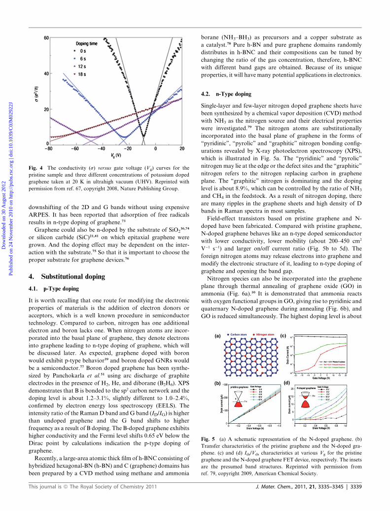
Fig. 4 The conductivity (s) versus gate voltage (Vg) curves for the
pristine sample and three different concentrations of potassium doped
graphene taken at 20 K in ultrahigh vacuum (UHV). Reprinted with
permission from ref. 67, copyright 2008, Nature Publishing Group.
Fig. 5 (a) A schematic representation of the N-doped graphene. (b)
Transfer characteristics of the pristine graphene and the N-doped gra-
phene. (c) and (d) Ids/Vds characteristics at various Vg for the pristine
graphene and the N-doped graphene FET device, respectively. The insets
are the presumed band structures. Reprinted with permission from
ref. 79, copyright 2009, American Chemical Society.
Dow
nloa
ded
on 3
0 A
ugus
t 201
2Pu
blis
hed
on 2
4 N
ovem
ber
2010
on
http
://pu
bs.r
sc.o
rg |
doi:1
0.10
39/C
0JM
0292
2J
View Online
downshifting of the 2D and G bands without using expensive
ARPES. It has been reported that adsorption of free radicals
results in n-type doping of graphene.73
Graphene could also be n-doped by the substrate of SiO236,74
or silicon carbide (SiC)21,41 on which epitaxial graphene were
grown. And the doping effect may be dependent on the inter-
action with the substrate.75 So that it is important to choose the
proper substrate for graphene devices.76
4. Substitutional doping
4.1. p-Type doping
It is worth recalling that one route for modifying the electronic
properties of materials is the addition of electron donors or
acceptors, which is a well known procedure in semiconductor
technology. Compared to carbon, nitrogen has one additional
electron and boron lacks one. When nitrogen atoms are incor-
porated into the basal plane of graphene, they denote electrons
into graphene leading to n-type doping of graphene, which will
be discussed later. As expected, graphene doped with boron
would exhibit p-type behavior39 and boron doped GNRs would
be a semiconductor.77 Boron doped graphene has been synthe-
sized by Panchokarla et al.51 using arc discharge of graphite
electrodes in the presence of H2, He, and diborane (B2H6). XPS
demonstrates that B is bonded to the sp2 carbon network and the
doping level is about 1.2–3.1%, slightly different to 1.0–2.4%,
confirmed by electron energy loss spectroscopy (EELS). The
intensity ratio of the Raman D band and G band (ID/IG) is higher
than undoped graphene and the G band shifts to higher
frequency as a result of B doping. The B-doped graphene exhibits
higher conductivity and the Fermi level shifts 0.65 eV below the
Dirac point by calculations indication the p-type doping of
graphene.
Recently, a large-area atomic thick film of h-BNC consisting of
hybridized hexagonal-BN (h-BN) and C (graphene) domains has
been prepared by a CVD method using methane and ammonia
This journal is ª The Royal Society of Chemistry 2011
borane (NH3–BH3) as precursors and a copper substrate as
a catalyst.78 Pure h-BN and pure graphene domains randomly
distributes in h-BNC and their compositions can be tuned by
changing the ratio of the gas concentration, therefore, h-BNC
with different band gaps are obtained. Because of its unique
properties, it will have many potential applications in electronics.
4.2. n-Type doping
Single-layer and few-layer nitrogen doped graphene sheets have
been synthesized by a chemical vapor deposition (CVD) method
with NH3 as the nitrogen source and their electrical properties
were investigated.79 The nitrogen atoms are substitutionally
incorporated into the basal plane of graphene in the forms of
‘‘pyridinic’’, ‘‘pyrolic’’ and ‘‘graphitic’’ nitrogen bonding config-
urations revealed by X-ray photoelectron spectroscopy (XPS),
which is illustrated in Fig. 5a. The ‘‘pyridinic’’ and ‘‘pyrolic’’
nitrogen may lie at the edge or the defect sites and the ‘‘graphitic’’
nitrogen refers to the nitrogen replacing carbon in graphene
plane. The ‘‘graphitic’’ nitrogen is dominating and the doping
level is about 8.9%, which can be controlled by the ratio of NH3
and CH4 in the feedstock. As a result of nitrogen doping, there
are many ripples in the graphene sheets and high density of D
bands in Raman spectra in most samples.
Field-effect transistors based on pristine graphene and N-
doped have been fabricated. Compared with pristine graphene,
N-doped graphene behaves like an n-type doped semiconductor
with lower conductivity, lower mobility (about 200–450 cm2
V�1 s�1) and larger on/off current ratio (Fig. 5b to 5d). The
foreign nitrogen atoms may release electrons into graphene and
modify the electronic structure of it, leading to n-type doping of
graphene and opening the band gap.
Nitrogen species can also be incorporated into the graphene
plane through thermal annealing of graphene oxide (GO) in
ammonia (Fig. 6a).10 It is demonstrated that ammonia reacts
with oxygen functional groups in GO, giving rise to pyridinic and
quaternary N-doped graphene during annealing (Fig. 6b), and
GO is reduced simultaneously. The highest doping level is about
J. Mater. Chem., 2011, 21, 3335–3345 | 3339
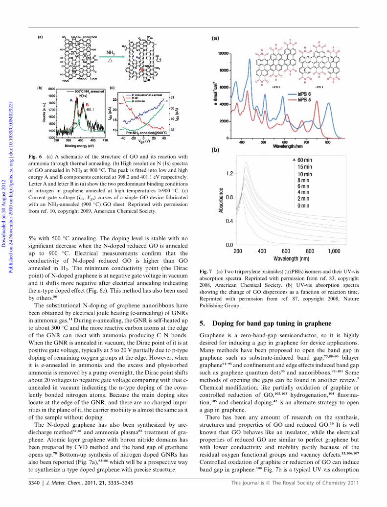
Fig. 6 (a) A schematic of the structure of GO and its reaction with
ammonia through thermal annealing. (b) High resolution N (1s) spectra
of GO annealed in NH3 at 900 �C. The peak is fitted into low and high
energy A and B components centered at 398.2 and 401.1 eV respectively.
Letter A and letter B in (a) show the two predominant binding conditions
of nitrogen in graphene annealed at high temperatures $900 �C. (c)
Current-gate voltage (Ids–Vgs) curves of a single GO device fabricated
with an NH3-annealed (900 �C) GO sheet. Reprinted with permission
from ref. 10, copyright 2009, American Chemical Society.
Fig. 7 (a) Two tri(perylene bisimides) (triPBIs) isomers and their UV-vis
absorption spectra. Reprinted with permission from ref. 83, copyright
2008, American Chemical Society. (b) UV-vis absorption spectra
showing the change of GO dispersions as a function of reaction time.
Reprinted with permission from ref. 87, copyright 2008, Nature
Publishing Group.
Dow
nloa
ded
on 3
0 A
ugus
t 201
2Pu
blis
hed
on 2
4 N
ovem
ber
2010
on
http
://pu
bs.r
sc.o
rg |
doi:1
0.10
39/C
0JM
0292
2J
View Online
5% with 500 �C annealing. The doping level is stable with no
significant decrease when the N-doped reduced GO is annealed
up to 900 �C. Electrical measurements confirm that the
conductivity of N-doped reduced GO is higher than GO
annealed in H2. The minimum conductivity point (the Dirac
point) of N-doped graphene is at negative gate voltage in vacuum
and it shifts more negative after electrical annealing indicating
the n-type doped effect (Fig. 6c). This method has also been used
by others.80
The substitutional N-doping of graphene nanoribbons have
been obtained by electrical joule heating (e-annealing) of GNRs
in ammonia gas.11 During e-annealing, the GNR is self-heated up
to about 300 �C and the more reactive carbon atoms at the edge
of the GNR can react with ammonia producing C–N bonds.
When the GNR is annealed in vacuum, the Dirac point of it is at
positive gate voltage, typically at 5 to 20 V partially due to p-type
doping of remaining oxygen groups at the edge. However, when
it is e-annealed in ammonia and the excess and physisorbed
ammonia is removed by a pump overnight, the Dirac point shifts
about 20 voltages to negative gate voltage comparing with that e-
annealed in vacuum indicating the n-type doping of the cova-
lently bonded nitrogen atoms. Because the main doping sites
locate at the edge of the GNR, and there are no charged impu-
rities in the plane of it, the carrier mobility is almost the same as it
of the sample without doping.
The N-doped graphene has also been synthesized by arc-
discharge method51,81 and ammonia plasma82 treatment of gra-
phene. Atomic layer graphene with boron nitride domains has
been prepared by CVD method and the band gap of graphene
opens up.78 Bottom-up synthesis of nitrogen doped GNRs has
also been reported (Fig. 7a),83–86 which will be a prospective way
to synthesize n-type doped graphene with precise structure.
3340 | J. Mater. Chem., 2011, 21, 3335–3345
5. Doping for band gap tuning in graphene
Graphene is a zero-band-gap semiconductor, so it is highly
desired for inducing a gap in graphene for device applications.
Many methods have been proposed to open the band gap in
graphene such as substrate-induced band gap,75,88–90 bilayer
graphene91–95 and confinement and edge effects induced band gap
such as graphene quantum dots96 and nanoribbons.97–101 Some
methods of opening the gaps can be found in another review.7
Chemical modification, like partially oxidation of graphite or
controlled reduction of GO,102,103 hydrogenation,104 fluorina-
tion,105 and chemical doping,42 is an alternate strategy to open
a gap in graphene.
There has been any amount of research on the synthesis,
structures and properties of GO and reduced GO.16 It is well
known that GO behaves like an insulator, while the electrical
properties of reduced GO are similar to perfect graphene but
with lower conductivity and mobility partly because of the
residual oxygen functional groups and vacancy defects.35,106,107
Controlled oxidation of graphite or reduction of GO can induce
band gap in graphene.108 Fig. 7b is a typical UV-vis adsorption
This journal is ª The Royal Society of Chemistry 2011
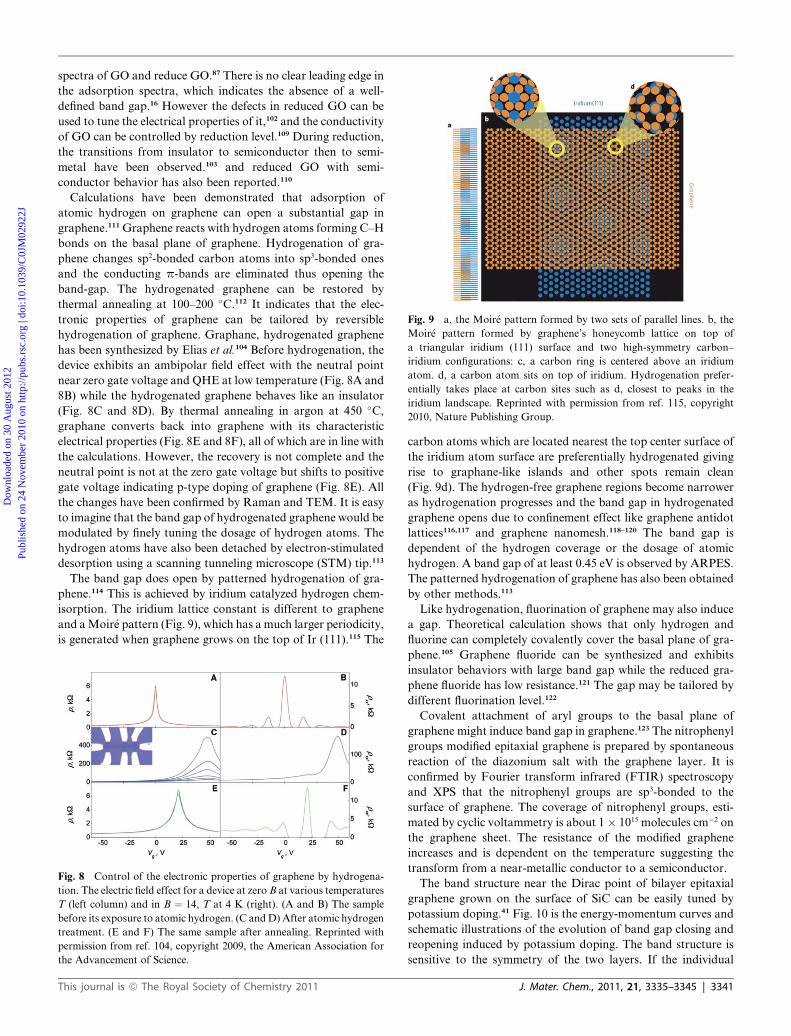
Fig. 9 a, the Moir�e pattern formed by two sets of parallel lines. b, the
Moir�e pattern formed by graphene’s honeycomb lattice on top of
a triangular iridium (111) surface and two high-symmetry carbon–
iridium configurations: c, a carbon ring is centered above an iridium
atom. d, a carbon atom sits on top of iridium. Hydrogenation prefer-
entially takes place at carbon sites such as d, closest to peaks in the
iridium landscape. Reprinted with permission from ref. 115, copyright
2010, Nature Publishing Group.
Dow
nloa
ded
on 3
0 A
ugus
t 201
2Pu
blis
hed
on 2
4 N
ovem
ber
2010
on
http
://pu
bs.r
sc.o
rg |
doi:1
0.10
39/C
0JM
0292
2J
View Online
spectra of GO and reduce GO.87 There is no clear leading edge in
the adsorption spectra, which indicates the absence of a well-
defined band gap.16 However the defects in reduced GO can be
used to tune the electrical properties of it,102 and the conductivity
of GO can be controlled by reduction level.109 During reduction,
the transitions from insulator to semiconductor then to semi-
metal have been observed.103 and reduced GO with semi-
conductor behavior has also been reported.110
Calculations have been demonstrated that adsorption of
atomic hydrogen on graphene can open a substantial gap in
graphene.111 Graphene reacts with hydrogen atoms forming C–H
bonds on the basal plane of graphene. Hydrogenation of gra-
phene changes sp2-bonded carbon atoms into sp3-bonded ones
and the conducting p-bands are eliminated thus opening the
band-gap. The hydrogenated graphene can be restored by
thermal annealing at 100–200 �C.112 It indicates that the elec-
tronic properties of graphene can be tailored by reversible
hydrogenation of graphene. Graphane, hydrogenated graphene
has been synthesized by Elias et al.104 Before hydrogenation, the
device exhibits an ambipolar field effect with the neutral point
near zero gate voltage and QHE at low temperature (Fig. 8A and
8B) while the hydrogenated graphene behaves like an insulator
(Fig. 8C and 8D). By thermal annealing in argon at 450 �C,
graphane converts back into graphene with its characteristic
electrical properties (Fig. 8E and 8F), all of which are in line with
the calculations. However, the recovery is not complete and the
neutral point is not at the zero gate voltage but shifts to positive
gate voltage indicating p-type doping of graphene (Fig. 8E). All
the changes have been confirmed by Raman and TEM. It is easy
to imagine that the band gap of hydrogenated graphene would be
modulated by finely tuning the dosage of hydrogen atoms. The
hydrogen atoms have also been detached by electron-stimulated
desorption using a scanning tunneling microscope (STM) tip.113
The band gap does open by patterned hydrogenation of gra-
phene.114 This is achieved by iridium catalyzed hydrogen chem-
isorption. The iridium lattice constant is different to graphene
and a Moir�e pattern (Fig. 9), which has a much larger periodicity,
is generated when graphene grows on the top of Ir (111).115 The
Fig. 8 Control of the electronic properties of graphene by hydrogena-
tion. The electric field effect for a device at zero B at various temperatures
T (left column) and in B ¼ 14, T at 4 K (right). (A and B) The sample
before its exposure to atomic hydrogen. (C and D) After atomic hydrogen
treatment. (E and F) The same sample after annealing. Reprinted with
permission from ref. 104, copyright 2009, the American Association for
the Advancement of Science.
This journal is ª The Royal Society of Chemistry 2011
carbon atoms which are located nearest the top center surface of
the iridium atom surface are preferentially hydrogenated giving
rise to graphane-like islands and other spots remain clean
(Fig. 9d). The hydrogen-free graphene regions become narrower
as hydrogenation progresses and the band gap in hydrogenated
graphene opens due to confinement effect like graphene antidot
lattices116,117 and graphene nanomesh.118–120 The band gap is
dependent of the hydrogen coverage or the dosage of atomic
hydrogen. A band gap of at least 0.45 eV is observed by ARPES.
The patterned hydrogenation of graphene has also been obtained
by other methods.113
Like hydrogenation, fluorination of graphene may also induce
a gap. Theoretical calculation shows that only hydrogen and
fluorine can completely covalently cover the basal plane of gra-
phene.105 Graphene fluoride can be synthesized and exhibits
insulator behaviors with large band gap while the reduced gra-
phene fluoride has low resistance.121 The gap may be tailored by
different fluorination level.122
Covalent attachment of aryl groups to the basal plane of
graphene might induce band gap in graphene.123 The nitrophenyl
groups modified epitaxial graphene is prepared by spontaneous
reaction of the diazonium salt with the graphene layer. It is
confirmed by Fourier transform infrared (FTIR) spectroscopy
and XPS that the nitrophenyl groups are sp3-bonded to the
surface of graphene. The coverage of nitrophenyl groups, esti-
mated by cyclic voltammetry is about 1� 1015 molecules cm�2 on
the graphene sheet. The resistance of the modified graphene
increases and is dependent on the temperature suggesting the
transform from a near-metallic conductor to a semiconductor.
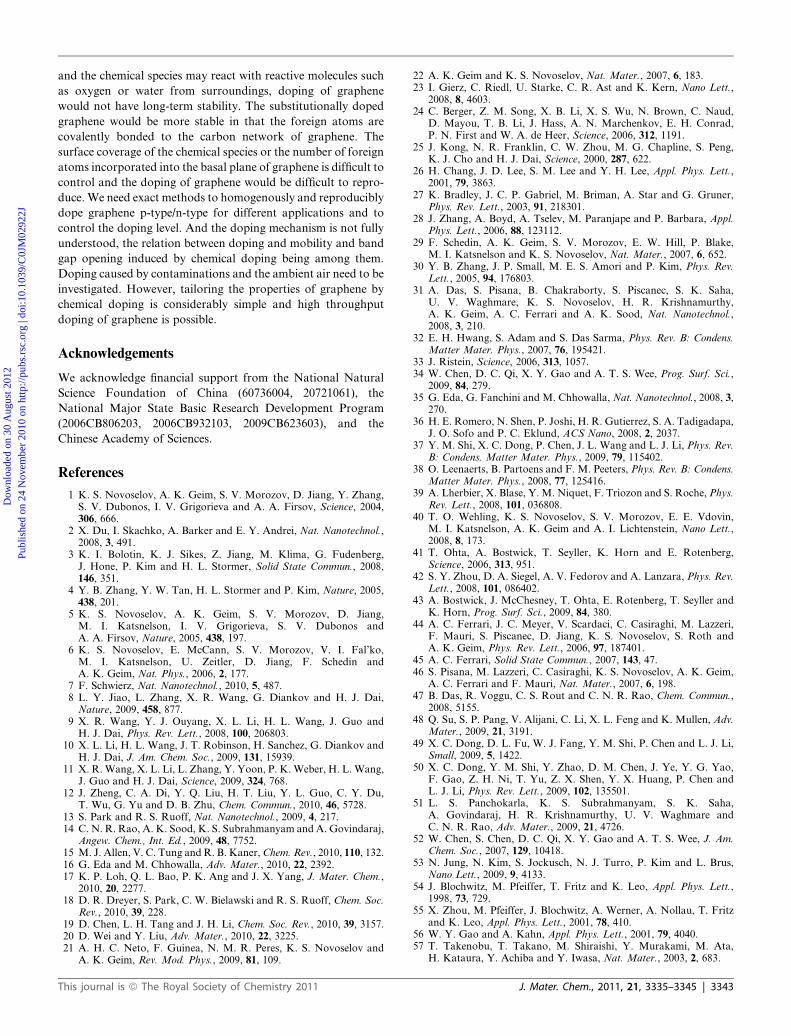
The band structure near the Dirac point of bilayer epitaxial
graphene grown on the surface of SiC can be easily tuned by
potassium doping.41 Fig. 10 is the energy-momentum curves and
schematic illustrations of the evolution of band gap closing and
reopening induced by potassium doping. The band structure is
sensitive to the symmetry of the two layers. If the individual
J. Mater. Chem., 2011, 21, 3335–3345 | 3341
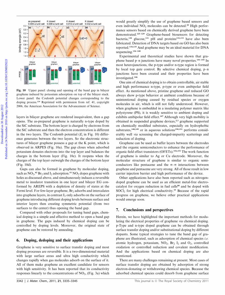
Fig. 10 Upper panel: closing and opening of the band gap in bilayer
graphene induced by potassium adsorption on top of the bilayer stack.
Lower panel: the Coulomb potential changes corresponding to the
doping process.124 Reprinted with permission from ref. 41, copyright
2006, the American Association for the Advancement of Science.
Dow
nloa
ded
on 3
0 A
ugus
t 201
2Pu
blis
hed
on 2
4 N
ovem
ber
2010
on
http
://pu
bs.r
sc.o
rg |
doi:1
0.10
39/C
0JM
0292
2J
View Online
layers in bilayer graphene are rendered inequivalent, then a gap
opens. The as-prepared graphene is naturally n-type doped by
the SiC substrate. The bottom layer is charged by electrons from
the SiC substrate and then the electron concentration is different
in the two layers. The Coulomb potential (Ei in Fig. 10) differ-
ence generates between the two layers. So the electronic struc-
tures of bilayer graphene possess a gap at the K point, which is
observed in ARPES (Fig. 10a). The gap closes when adsorbed
potassium donates electrons into the top layer and balances the
charges in the bottom layer (Fig. 10c). It reopens when the
charges of the top layer outweigh the charges of the bottom layer
(Fig. 10d).
Gaps can also be formed in graphene by molecular doping,
such as NO2,42 Br2 and I2 adsorption.53 NO2 dopes graphene with
holes as discussed above, and simultaneously induces a reversible
metal to insulator transition in one layer and bilayer EG con-
formed by AREPS with a depletion of density of states at the
Fermi level. For few-layer graphene, Br2 adsorbs and intercalates
into graphene layers, in contrast I2 only adsorbs on the surface of
graphene introducing different doping levels between surface and
interior layers then creating symmetric potential (from two
surfaces to the center) thus opening the band gap.
Compared with other proposals for tuning band gaps, chem-
ical doping is a simple and effective method to open a band gap
in graphene. The gaps induced by chemical doping can be
controlled by doping levels. Moreover, the original state of
graphene can be restored by annealing.
6. Doping, dedoping and their applications
Graphene is very sensitive to surface transfer doping and most
doping processes are reversible. It is a two-dimensional material
with large surface areas and ultra high conductivity which
changes rapidly when gas molecules adsorb on the surface of it.
All of them make graphene an excellent candidate for sensors
with high sensitivity. It has been reported that its conductivity
responses linearly to the concentrations of NO2, (Fig. 3a) which
3342 | J. Mater. Chem., 2011, 21, 3335–3345
would greatly simplify the use of graphene based sensors and
even individual NO2 molecules can be detected.29 High perfor-
mance sensors based on chemically derived graphene have been
demonstrated.125–129 Graphene-based biosensors for detecting
bacteria,130 glucose,131 pH and proteins132,133 have also been
fabricated. Detection of DNA targets based on GO has also been
reported.134,135 And graphene may be an ideal material for DNA
sequencing.136–140
Experimental and theoretical studies have shown that gra-
phene based p–n junctions have many novel properties.141–145 In
most heterojunctions, the p-type and/or n-type region is formed
by local top gate control. By selective chemical doping, p–n
junctions have been created and their properties have been
investigated.146
One aim of chemical doping is to obtain controllable, air stable
and high performance n-type, p-type or even ambipolar field
effect. As mentioned above, pristine graphene and reduced GO
always show p-type behavior at ambient conditions because of
unintentional doping caused by residual species or oxygen
molecules in air, which is still not fully understood. However,
when graphene is embedded in a insulating polymer matrix like
polystyrene (PS), it is weakly sensitive to ambient doping and
exhibits ambipolar field effect.147 Although very high mobility is
obtained in suspended graphene devices,2,3 graphene supported
on chemically modified substrates, especially on hydrophobic
substrates,148,149 or in aqueous solutions150,151 performs consid-
erably well via screening the charged-impurity scatterings and
reduction of doping.
Graphene can be used as buffer layers between the electrodes
and the organic semiconductors to enhance the performance of
organic field effect transistors (OFETs).152,153 The work function
of graphene is similar to Ag or Cu electrode. Moreover, the
molecular structure of graphene is similar to organic semi-
conductors like pentacene and the p–p interactions between
graphene and pentacene are very strong. All of those result in low
carrier injection barrier and high performance of the device.
Other applications have also been reported such as nitrogen-
doped graphene can be used as an efficient metal-free electro-
catalyst for oxygen reduction in fuel cells80 and be doped with
SOCl2 for high electrical conductivity.35 Because of the rapid
progress on graphene, we believe other practical applications
would emerge soon.
7. Conclusions and perspectives
Herein, we have highlighted the important methods for modu-
lating the electrical properties of graphene via chemical doping.
p-Type and n-type doped graphene can be obtained through
surface transfer doping and/or substitutional doping by different
dopants. Some typical strategies to tune the band gap of gra-
phene are illustrated, such as adsorption of chemical species i.e.
atomic hydrogen, potassium, NO2, Br2 I2 and O2, controlled
oxidation or controlled reduction and covalent modification.
And the applications based on chemical doping are also
mentioned.
There are many challenges remaining at present. Most cases of
surface transfer doping are obtained by adsorption of strong
electron-donating or withdrawing chemical species. Because the
adsorbed chemical species could desorb from graphene surface
This journal is ª The Royal Society of Chemistry 2011
Dow
nloa
ded
on 3
0 A
ugus
t 201
2Pu
blis
hed
on 2
4 N
ovem
ber
2010
on
http
://pu
bs.r
sc.o
rg |
doi:1
0.10
39/C
0JM
0292
2J
View Online
and the chemical species may react with reactive molecules such
as oxygen or water from surroundings, doping of graphene
would not have long-term stability. The substitutionally doped
graphene would be more stable in that the foreign atoms are
covalently bonded to the carbon network of graphene. The
surface coverage of the chemical species or the number of foreign
atoms incorporated into the basal plane of graphene is difficult to
control and the doping of graphene would be difficult to repro-
duce. We need exact methods to homogenously and reproducibly
dope graphene p-type/n-type for different applications and to
control the doping level. And the doping mechanism is not fully
understood, the relation between doping and mobility and band
gap opening induced by chemical doping being among them.
Doping caused by contaminations and the ambient air need to be
investigated. However, tailoring the properties of graphene by
chemical doping is considerably simple and high throughput
doping of graphene is possible.
Acknowledgements
We acknowledge financial support from the National Natural
Science Foundation of China (60736004, 20721061), the
National Major State Basic Research Development Program
(2006CB806203, 2006CB932103, 2009CB623603), and the
Chinese Academy of Sciences.
References
1 K. S. Novoselov, A. K. Geim, S. V. Morozov, D. Jiang, Y. Zhang,S. V. Dubonos, I. V. Grigorieva and A. A. Firsov, Science, 2004,306, 666.
2 X. Du, I. Skachko, A. Barker and E. Y. Andrei, Nat. Nanotechnol.,2008, 3, 491.
3 K. I. Bolotin, K. J. Sikes, Z. Jiang, M. Klima, G. Fudenberg,J. Hone, P. Kim and H. L. Stormer, Solid State Commun., 2008,146, 351.
4 Y. B. Zhang, Y. W. Tan, H. L. Stormer and P. Kim, Nature, 2005,438, 201.
5 K. S. Novoselov, A. K. Geim, S. V. Morozov, D. Jiang,M. I. Katsnelson, I. V. Grigorieva, S. V. Dubonos andA. A. Firsov, Nature, 2005, 438, 197.
6 K. S. Novoselov, E. McCann, S. V. Morozov, V. I. Fal’ko,M. I. Katsnelson, U. Zeitler, D. Jiang, F. Schedin andA. K. Geim, Nat. Phys., 2006, 2, 177.
7 F. Schwierz, Nat. Nanotechnol., 2010, 5, 487.8 L. Y. Jiao, L. Zhang, X. R. Wang, G. Diankov and H. J. Dai,
Nature, 2009, 458, 877.9 X. R. Wang, Y. J. Ouyang, X. L. Li, H. L. Wang, J. Guo and
H. J. Dai, Phys. Rev. Lett., 2008, 100, 206803.10 X. L. Li, H. L. Wang, J. T. Robinson, H. Sanchez, G. Diankov and
H. J. Dai, J. Am. Chem. Soc., 2009, 131, 15939.11 X. R. Wang, X. L. Li, L. Zhang, Y. Yoon, P. K. Weber, H. L. Wang,
J. Guo and H. J. Dai, Science, 2009, 324, 768.12 J. Zheng, C. A. Di, Y. Q. Liu, H. T. Liu, Y. L. Guo, C. Y. Du,
T. Wu, G. Yu and D. B. Zhu, Chem. Commun., 2010, 46, 5728.13 S. Park and R. S. Ruoff, Nat. Nanotechnol., 2009, 4, 217.14 C. N. R. Rao, A. K. Sood, K. S. Subrahmanyam and A. Govindaraj,
Angew. Chem., Int. Ed., 2009, 48, 7752.15 M. J. Allen, V. C. Tung and R. B. Kaner, Chem. Rev., 2010, 110, 132.16 G. Eda and M. Chhowalla, Adv. Mater., 2010, 22, 2392.17 K. P. Loh, Q. L. Bao, P. K. Ang and J. X. Yang, J. Mater. Chem.,
2010, 20, 2277.18 D. R. Dreyer, S. Park, C. W. Bielawski and R. S. Ruoff, Chem. Soc.
Rev., 2010, 39, 228.19 D. Chen, L. H. Tang and J. H. Li, Chem. Soc. Rev., 2010, 39, 3157.20 D. Wei and Y. Liu, Adv. Mater., 2010, 22, 3225.21 A. H. C. Neto, F. Guinea, N. M. R. Peres, K. S. Novoselov and
A. K. Geim, Rev. Mod. Phys., 2009, 81, 109.
This journal is ª The Royal Society of Chemistry 2011
22 A. K. Geim and K. S. Novoselov, Nat. Mater., 2007, 6, 183.23 I. Gierz, C. Riedl, U. Starke, C. R. Ast and K. Kern, Nano Lett.,
2008, 8, 4603.24 C. Berger, Z. M. Song, X. B. Li, X. S. Wu, N. Brown, C. Naud,
D. Mayou, T. B. Li, J. Hass, A. N. Marchenkov, E. H. Conrad,P. N. First and W. A. de Heer, Science, 2006, 312, 1191.
25 J. Kong, N. R. Franklin, C. W. Zhou, M. G. Chapline, S. Peng,K. J. Cho and H. J. Dai, Science, 2000, 287, 622.
26 H. Chang, J. D. Lee, S. M. Lee and Y. H. Lee, Appl. Phys. Lett.,2001, 79, 3863.
27 K. Bradley, J. C. P. Gabriel, M. Briman, A. Star and G. Gruner,Phys. Rev. Lett., 2003, 91, 218301.
28 J. Zhang, A. Boyd, A. Tselev, M. Paranjape and P. Barbara, Appl.Phys. Lett., 2006, 88, 123112.
29 F. Schedin, A. K. Geim, S. V. Morozov, E. W. Hill, P. Blake,M. I. Katsnelson and K. S. Novoselov, Nat. Mater., 2007, 6, 652.
30 Y. B. Zhang, J. P. Small, M. E. S. Amori and P. Kim, Phys. Rev.Lett., 2005, 94, 176803.
31 A. Das, S. Pisana, B. Chakraborty, S. Piscanec, S. K. Saha,U. V. Waghmare, K. S. Novoselov, H. R. Krishnamurthy,A. K. Geim, A. C. Ferrari and A. K. Sood, Nat. Nanotechnol.,2008, 3, 210.
32 E. H. Hwang, S. Adam and S. Das Sarma, Phys. Rev. B: Condens.Matter Mater. Phys., 2007, 76, 195421.
33 J. Ristein, Science, 2006, 313, 1057.34 W. Chen, D. C. Qi, X. Y. Gao and A. T. S. Wee, Prog. Surf. Sci.,
2009, 84, 279.35 G. Eda, G. Fanchini and M. Chhowalla, Nat. Nanotechnol., 2008, 3,
270.36 H. E. Romero, N. Shen, P. Joshi, H. R. Gutierrez, S. A. Tadigadapa,
J. O. Sofo and P. C. Eklund, ACS Nano, 2008, 2, 2037.37 Y. M. Shi, X. C. Dong, P. Chen, J. L. Wang and L. J. Li, Phys. Rev.
B: Condens. Matter Mater. Phys., 2009, 79, 115402.38 O. Leenaerts, B. Partoens and F. M. Peeters, Phys. Rev. B: Condens.
Matter Mater. Phys., 2008, 77, 125416.39 A. Lherbier, X. Blase, Y. M. Niquet, F. Triozon and S. Roche, Phys.
Rev. Lett., 2008, 101, 036808.40 T. O. Wehling, K. S. Novoselov, S. V. Morozov, E. E. Vdovin,
M. I. Katsnelson, A. K. Geim and A. I. Lichtenstein, Nano Lett.,2008, 8, 173.
41 T. Ohta, A. Bostwick, T. Seyller, K. Horn and E. Rotenberg,Science, 2006, 313, 951.
42 S. Y. Zhou, D. A. Siegel, A. V. Fedorov and A. Lanzara, Phys. Rev.Lett., 2008, 101, 086402.
43 A. Bostwick, J. McChesney, T. Ohta, E. Rotenberg, T. Seyller andK. Horn, Prog. Surf. Sci., 2009, 84, 380.
44 A. C. Ferrari, J. C. Meyer, V. Scardaci, C. Casiraghi, M. Lazzeri,F. Mauri, S. Piscanec, D. Jiang, K. S. Novoselov, S. Roth andA. K. Geim, Phys. Rev. Lett., 2006, 97, 187401.
45 A. C. Ferrari, Solid State Commun., 2007, 143, 47.46 S. Pisana, M. Lazzeri, C. Casiraghi, K. S. Novoselov, A. K. Geim,
A. C. Ferrari and F. Mauri, Nat. Mater., 2007, 6, 198.47 B. Das, R. Voggu, C. S. Rout and C. N. R. Rao, Chem. Commun.,
2008, 5155.48 Q. Su, S. P. Pang, V. Alijani, C. Li, X. L. Feng and K. Mullen, Adv.
Mater., 2009, 21, 3191.49 X. C. Dong, D. L. Fu, W. J. Fang, Y. M. Shi, P. Chen and L. J. Li,
Small, 2009, 5, 1422.50 X. C. Dong, Y. M. Shi, Y. Zhao, D. M. Chen, J. Ye, Y. G. Yao,
F. Gao, Z. H. Ni, T. Yu, Z. X. Shen, Y. X. Huang, P. Chen andL. J. Li, Phys. Rev. Lett., 2009, 102, 135501.
51 L. S. Panchokarla, K. S. Subrahmanyam, S. K. Saha,A. Govindaraj, H. R. Krishnamurthy, U. V. Waghmare andC. N. R. Rao, Adv. Mater., 2009, 21, 4726.
52 W. Chen, S. Chen, D. C. Qi, X. Y. Gao and A. T. S. Wee, J. Am.Chem. Soc., 2007, 129, 10418.
53 N. Jung, N. Kim, S. Jockusch, N. J. Turro, P. Kim and L. Brus,Nano Lett., 2009, 9, 4133.
54 J. Blochwitz, M. Pfeiffer, T. Fritz and K. Leo, Appl. Phys. Lett.,1998, 73, 729.
55 X. Zhou, M. Pfeiffer, J. Blochwitz, A. Werner, A. Nollau, T. Fritzand K. Leo, Appl. Phys. Lett., 2001, 78, 410.
56 W. Y. Gao and A. Kahn, Appl. Phys. Lett., 2001, 79, 4040.57 T. Takenobu, T. Takano, M. Shiraishi, Y. Murakami, M. Ata,
H. Kataura, Y. Achiba and Y. Iwasa, Nat. Mater., 2003, 2, 683.
J. Mater. Chem., 2011, 21, 3335–3345 | 3343
Dow
nloa
ded
on 3
0 A
ugus
t 201
2Pu
blis
hed
on 2
4 N
ovem
ber
2010
on
http
://pu
bs.r
sc.o
rg |
doi:1
0.10
39/C
0JM
0292
2J
View Online
58 W. Y. Gao and A. Kahn, J. Appl. Phys., 2003, 94, 359.59 T. Takenobu, T. Kanbara, N. Akima, T. Takahashi, M. Shiraishi,
K. Tsukagoshi, H. Kataura, Y. Aoyagi and Y. Iwasa, Adv. Mater.,2005, 17, 2430.
60 H. Pinto, R. Jones, J. P. Goss and P. R. Briddon, J. Phys.: Condens.Matter, 2009, 21, 402001.
61 C. Coletti, C. Riedl, D. S. Lee, B. Krauss, L. Patthey, K. vonKlitzing, J. H. Smet and U. Starke, Phys. Rev. B: Condens. MatterMater. Phys., 2010, 81, 235401.
62 Y. H. Lu, W. Chen, Y. P. Feng and P. M. He, J. Phys. Chem. B,2009, 113, 2.
63 H. T. Liu, S. M. Ryu, Z. Y. Chen, M. L. Steigerwald, C. Nuckollsand L. E. Brus, J. Am. Chem. Soc., 2009, 131, 17099.
64 L. Liu, S. M. Ryu, M. R. Tomasik, E. Stolyarova, N. Jung,M. S. Hybertsen, M. L. Steigerwald, L. E. Brus and G. W. Flynn,Nano Lett., 2008, 8, 1965.
65 D. B. Farmer, R. Golizadeh-Mojarad, V. Perebeinos, Y. M. Lin,G. S. Tulevski, J. C. Tsang and P. Avouris, Nano Lett., 2009, 9, 388.
66 B. Lee, Y. Chen, F. Duerr, D. Mastrogiovanni, E. Garfunkel,E. Y. Andrei and V. Podzorov, Nano Lett., 2010, 10, 2427.
67 J. H. Chen, C. Jang, S. Adam, M. S. Fuhrer, E. D. Williams andM. Ishigami, Nat. Phys., 2008, 4, 377.
68 A. Benayad, H. J. Shin, H. K. Park, S. M. Yoon, K. K. Kim,M. H. Jin, H. K. Jeong, J. C. Lee, J. Y. Choi and Y. H. Lee,Chem. Phys. Lett., 2009, 475, 91.
69 G. Giovannetti, P. A. Khomyakov, G. Brocks, V. M. Karpan, J. vanden Brink and P. J. Kelly, Phys. Rev. Lett., 2008, 101, 026803.
70 H. E. Romero, P. Joshi, A. K. Gupta, H. R. Gutierrez, M. W. Cole,S. A. Tadigadapa and P. C. Eklund, Nanotechnology, 2009, 20,245501.
71 A. Bostwick, T. Ohta, T. Seyller, K. Horn and E. Rotenberg, Nat.Phys., 2007, 3, 36.
72 M. Shim, A. Javey, N. W. S. Kam and H. J. Dai, J. Am. Chem. Soc.,2001, 123, 11512.
73 J. Choi, H. Lee, K. J. Kim, B. Kim and S. Kim, J. Phys. Chem. Lett.,2010, 1, 505.
74 T. O. Wehling, A. I. Lichtenstein and M. I. Katsnelson, Appl. Phys.Lett., 2008, 93, 202110.
75 S. Y. Zhou, G. H. Gweon, A. V. Fedorov, P. N. First, W. A. DeHeer, D. H. Lee, F. Guinea, A. H. C. Neto and A. Lanzara, Nat.Mater., 2007, 6, 770.
76 J. H. Chen, C. Jang, S. D. Xiao, M. Ishigami and M. S. Fuhrer, Nat.Nanotechnol., 2008, 3, 206.
77 T. B. Martins, R. H. Miwa, A. J. R. da Silva and A. Fazzio, Phys.Rev. Lett., 2007, 98, 196803.
78 L. Ci, L. Song, C. H. Jin, D. Jariwala, D. X. Wu, Y. J. Li,A. Srivastava, Z. F. Wang, K. Storr, L. Balicas, F. Liu andP. M. Ajayan, Nat. Mater., 2010, 9, 430.
79 D. C. Wei, Y. Q. Liu, Y. Wang, H. L. Zhang, L. P. Huang andG. Yu, Nano Lett., 2009, 9, 1752.
80 L. T. Qu, Y. Liu, J. B. Baek and L. M. Dai, ACS Nano, 2010, 4, 1321.81 N. Li, Z. Y. Wang, K. K. Zhao, Z. J. Shi, Z. N. Gu and S. K. Xu,
Carbon, 2010, 48, 255.82 Y. C. Lin, C. Y. Lin and P. W. Chiu, Appl. Phys. Lett., 2010, 96,
133110.83 H. L. Qian, F. Negri, C. R. Wang and Z. H. Wang, J. Am. Chem.
Soc., 2008, 130, 17970.84 A. Tsuda and A. Osuka, Science, 2001, 293, 79.85 Y. Li and Z. H. Wang, Org. Lett., 2009, 11, 1385.86 Y. G. Zhen, C. R. Wang and Z. H. Wang, Chem. Commun., 2010, 46,
1926.87 D. Li, M. B. Muller, S. Gilje, R. B. Kaner and G. G. Wallace, Nat.
Nanotechnol., 2008, 3, 101.88 S. Y. Zhou, D. A. Siegel, A. V. Fedorov, F. El Gabaly,
A. K. Schmid, A. H. C. Neto, D. H. Lee and A. Lanzara, Nat.Mater., 2008, 7, 259.
89 S. Kim, J. Ihm, H. J. Choi and Y. W. Son, Phys. Rev. Lett., 2008,100, 176802.
90 S. Y. Kwon, C. V. Ciobanu, V. Petrova, V. B. Shenoy, J. Bareno,V. Gambin, I. Petrov and S. Kodambaka, Nano Lett., 2009, 9, 3985.
91 E. McCann, Phys. Rev. B: Condens. Matter Mater. Phys., 2006, 74,161403.
92 E. V. Castro, K. S. Novoselov, S. V. Morozov, N. M. R. Peres,J. Dos Santos, J. Nilsson, F. Guinea, A. K. Geim andA. H. C. Neto, Phys. Rev. Lett., 2007, 99, 216802.
3344 | J. Mater. Chem., 2011, 21, 3335–3345
93 J. B. Oostinga, H. B. Heersche, X. L. Liu, A. F. Morpurgo andL. M. K. Vandersypen, Nat. Mater., 2008, 7, 151.
94 Y. B. Zhang, T. T. Tang, C. Girit, Z. Hao, M. C. Martin, A. Zettl,M. F. Crommie, Y. R. Shen and F. Wang, Nature, 2009, 459, 820.
95 F. N. Xia, D. B. Farmer, Y. M. Lin and P. Avouris, Nano Lett.,2010, 10, 715.
96 L. A. Ponomarenko, F. Schedin, M. I. Katsnelson, R. Yang,E. W. Hill, K. S. Novoselov and A. K. Geim, Science, 2008, 320, 356.
97 K. Nakada, M. Fujita, G. Dresselhaus and M. S. Dresselhaus, Phys.Rev. B: Condens. Matter, 1996, 54, 17954.
98 V. Barone, O. Hod and G. E. Scuseria, Nano Lett., 2006, 6, 2748.99 Y. W. Son, M. L. Cohen and S. G. Louie, Phys. Rev. Lett., 2006, 97,
216803.100 M. Y. Han, B. Ozyilmaz, Y. B. Zhang and P. Kim, Phys. Rev. Lett.,
2007, 98, 206805.101 X. L. Li, X. R. Wang, L. Zhang, S. W. Lee and H. J. Dai, Science,
2008, 319, 1229.102 S. Wang, P. J. Chia, L. L. Chua, L. H. Zhao, R. Q. Png,
S. Sivaramakrishnan, M. Zhou, R. G. S. Goh, R. H. Friend,A. T. S. Wee and P. K. H. Ho, Adv. Mater., 2008, 20, 3440.
103 G. Eda, C. Mattevi, H. Yamaguchi, H. Kim and M. Chhowalla, J.Phys. Chem. C, 2009, 113, 15768.
104 D. C. Elias, R. R. Nair, T. M. G. Mohiuddin, S. V. Morozov,P. Blake, M. P. Halsall, A. C. Ferrari, D. W. Boukhvalov,M. I. Katsnelson, A. K. Geim and K. S. Novoselov, Science, 2009,323, 610.
105 D. W. Boukhvalov and M. I. Katsnelson, J. Phys.: Condens. Matter,2009, 21, 344205.
106 C. Gomez-Navarro, R. T. Weitz, A. M. Bittner, M. Scolari,A. Mews, M. Burghard and K. Kern, Nano Lett., 2007, 7, 3499.
107 H. L. Wang, J. T. Robinson, X. L. Li and H. J. Dai, J. Am. Chem.Soc., 2009, 131, 9910.
108 J. A. Yan, L. D. Xian and M. Y. Chou, Phys. Rev. Lett., 2009, 103,086802.
109 I. Jung, D. A. Dikin, R. D. Piner and R. S. Ruoff, Nano Lett., 2008,8, 4283.
110 S. Gilje, S. Han, M. Wang, K. L. Wang and R. B. Kaner, Nano Lett.,2007, 7, 3394.
111 E. J. Duplock, M. Scheffler and P. J. D. Lindan, Phys. Rev. Lett.,2004, 92, 225502.
112 S. Ryu, M. Y. Han, J. Maultzsch, T. F. Heinz, P. Kim,M. L. Steigerwald and L. E. Brus, Nano Lett., 2008, 8, 4597.
113 P. Sessi, J. R. Guest, M. Bode and N. P. Guisinger, Nano Lett., 2009,9, 4343.
114 R. Balog, B. Jorgensen, L. Nilsson, M. Andersen, E. Rienks,M. Bianchi, M. Fanetti, E. Laegsgaard, A. Baraldi, S. Lizzit,Z. Sljivancanin, F. Besenbacher, B. Hammer, T. G. Pedersen,P. Hofmann and L. Hornekaer, Nat. Mater., 2010, 9, 315.
115 J. van den Brink, Nat. Mater., 2010, 9, 291.116 J. Eroms and D. Weiss, New J. Phys., 2009, 11, 095021.117 M. Vanevic, V. M. Stojanovic and M. Kindermann, Phys. Rev. B:
Condens. Matter Mater. Phys., 2009, 80, 045410.118 J. W. Bai, X. Zhong, S. Jiang, Y. Huang and X. F. Duan, Nat.
Nanotechnol., 2010, 5, 190.119 A. J. Du, Z. H. Zhu and S. C. Smith, J. Am. Chem. Soc., 2010, 132,
2876.120 M. Kim, N. S. Safron, E. Han, M. S. Arnold and P. Gopalan, Nano
Lett., 2010, 10, 1125.121 S. H. Cheng, K. Zou, F. Okino, H. R. Gutierrez, A. Gupta, N. Shen,
P. C. Eklund, J. O. Sofo and J. Zhu, Phys. Rev. B: Condens. MatterMater. Phys., 2010, 81, 205435.
122 J. T. Robinson, J. S. Burgess, C. E. Junkermeier, S. C. Badescu,T. L. Reinecke, F. K. Perkins, M. K. Zalalutdniov, J. W. Baldwin,J. C. Culbertson, P. E. Sheehan and E. S. Snow, Nano Lett., 2010,10, 3001.
123 E. Bekyarova, M. E. Itkis, P. Ramesh, C. Berger, M. Sprinkle,W. A. de Heer and R. C. Haddon, J. Am. Chem. Soc., 2009, 131,1336.
124 T. Seyller, A. Bostwick, K. V. Emtsev, K. Horn, L. Ley,J. L. McChesney, T. Ohta, J. D. Riley, E. Rotenberg andF. Speck, Phys. Status Solidi B, 2008, 245, 1436.
125 J. T. Robinson, F. K. Perkins, E. S. Snow, Z. Q. Wei andP. E. Sheehan, Nano Lett., 2008, 8, 3137.
126 R. S. Sundaram, C. Gomez-Navarro, K. Balasubranianian,M. Burghard and K. Kern, Adv. Mater., 2008, 20, 3050.
This journal is ª The Royal Society of Chemistry 2011
Dow
nloa
ded
on 3
0 A
ugus
t 201
2Pu
blis
hed
on 2
4 N
ovem
ber
2010
on
http
://pu
bs.r
sc.o
rg |
doi:1
0.10
39/C
0JM
0292
2J
View Online
127 J. D. Fowler, M. J. Allen, V. C. Tung, Y. Yang, R. B. Kaner andB. H. Weiller, ACS Nano, 2009, 3, 301.
128 G. H. Lu, L. E. Ocola and J. H. Chen, Appl. Phys. Lett., 2009, 94,083111.
129 G. H. Lu, L. E. Ocola and J. H. Chen, Nanotechnology, 2009, 20, 445502.130 N. Mohanty and V. Berry, Nano Lett., 2008, 8, 4469.131 Y. Wang, Y. Y. Shao, D. W. Matson, J. H. Li and Y. H. Lin, ACS
Nano, 2010, 4, 1790.132 P. K. Ang, W. Chen, A. T. S. Wee and K. P. Loh, J. Am. Chem. Soc.,
2008, 130, 14392.133 Y. Ohno, K. Maehashi, Y. Yamashiro and K. Matsumoto, Nano
Lett., 2009, 9, 3318.134 C. H. Lu, H. H. Yang, C. L. Zhu, X. Chen and G. N. Chen, Angew.
Chem., Int. Ed., 2009, 48, 4785.135 S. He, B. Song, D. Li, C. Zhu, W. Qi, Y. Wen, L. Wang, S. Song,
H. Fang and C. Fan, Adv. Mater., 2010, 20, 453.136 M. S. Xu, D. Fujita and N. Hanagata, Small, 2009, 5, 2638.137 H. W. C. Postma, Nano Lett., 2010, 10, 420.138 G. F. Schneider, S. W. Kowalczyk, V. E. Calado, G. Pandraud,
H. W. Zandbergen, L. M. K. Vandersypen and C. Dekker, NanoLett., 2010, 10, 3163.
139 C. A. Merchant, K. Healy, M. Wanunu, V. Ray, N. Peterman,J. Bartel, M. D. Fischbein, K. Venta, Z. T. Luo, A. T. C. Johnsonand M. Drndic, Nano Lett., 2010, 10, 2915.
This journal is ª The Royal Society of Chemistry 2011
140 S. Garaj, W. Hubbard, A. Reina, J. Kong, D. Branton andJ. A. Golovchenko, Nature, 2010, 467, 190.
141 V. V. Cheianov and V. I. Fal’ko, Phys. Rev. B: Condens. MatterMater. Phys., 2006, 74, 041403.
142 V. V. Cheianov, V. Fal’ko and B. L. Altshuler, Science, 2007, 315,1252.
143 J. R. Williams, L. DiCarlo and C. M. Marcus, Science, 2007, 317,638.
144 D. A. Abanin and L. S. Levitov, Science, 2007, 317, 641.145 A. F. Young and P. Kim, Nat. Phys., 2009, 5, 222.146 T. Lohmann, K. von Klitzing and J. H. Smet, Nano Lett., 2009, 9,
1973.147 G. Eda and M. Chhowalla, Nano Lett., 2009, 9, 814.148 S. S. Sabri, P. L. Levesque, C. M. Aguirre, J. Guillemette, R. Martel
and T. Szkopek, Appl. Phys. Lett., 2009, 95, 242104.149 M. Lafkioti, B. Krauss, T. Lohmann, U. Zschieschang, H. Klauk,
K. von Klitzing and J. H. Smet, Nano Lett., 2010, 10, 1149.150 F. Chen, J. L. Xia and N. J. Tao, Nano Lett., 2009, 9, 1621.151 S. Wang, P. K. Ang, Z. Q. Wang, A. L. L. Tang, J. T. L. Thong and
K. P. Loh, Nano Lett., 2010, 10, 92.152 C. A. Di, D. C. Wei, G. Yu, Y. Q. Liu, Y. L. Guo and D. B. Zhu,
Adv. Mater., 2008, 20, 3289.153 C. A. Di, Y. Q. Liu, G. Yu and D. B. Zhu, Acc. Chem. Res., 2009, 42,
1573.
J. Mater. Chem., 2011, 21, 3335–3345 | 3345