Embed Size (px)
Citation preview
1
Chapter 5
Image Capturing System
2
Image Capturing Technique – Objectives Types of image capturing technique
Charge-Coupled Device CMOS CCD vs CMOS image sensors
Types of image capturing system Digital Camera Biometric Devices
3
Image Capturing Technique – Introduction Currently, the type of image capturing techniques
available for today markets are: Contact image sensor (CIS) Charge-coupled device (CCD) array CMOS Image sensor
4
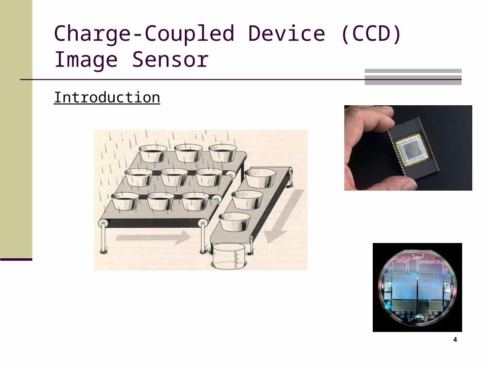
Charge-Coupled Device (CCD) Image Sensor
Introduction
5
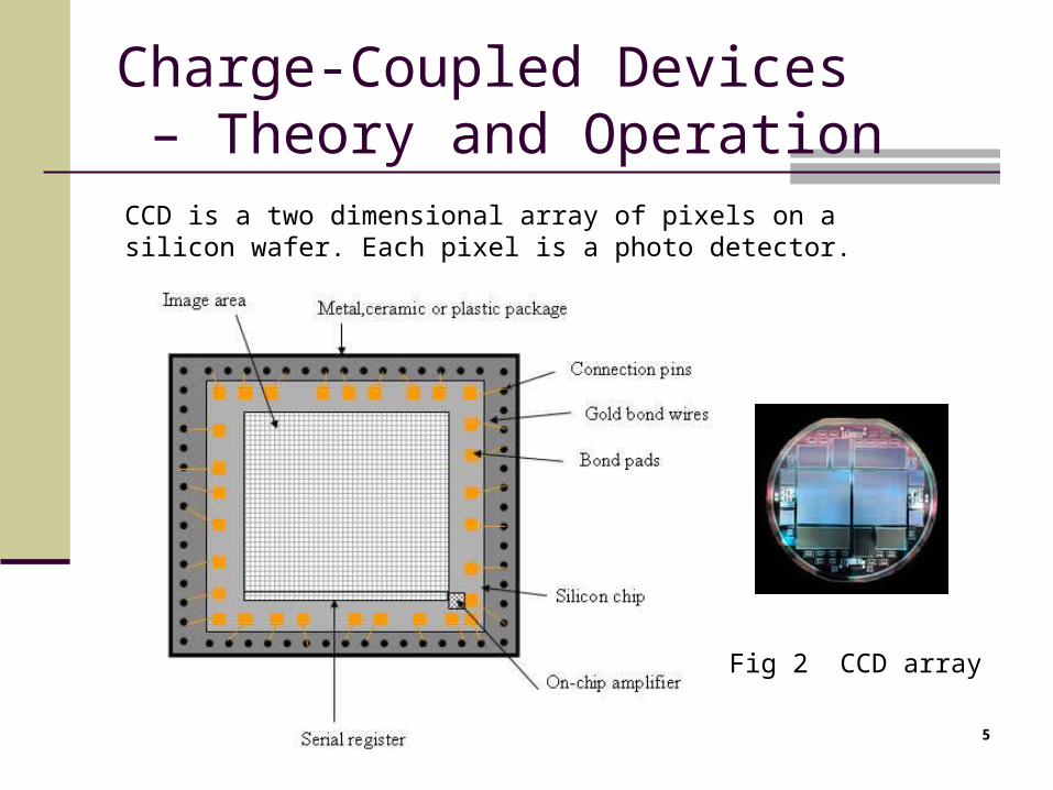
Charge-Coupled Devices – Theory and OperationCCD is a two dimensional array of pixels on a silicon wafer. Each pixel is a photo detector.
Fig 2 CCD array
6
Charge-Coupled Devices – Theory and Operation Converting light(Photon) to Electric Charge
Image is acquired when incident light (photon) falls on the array of pixels.
it translates this information into electrons (electrical charges).
A brighter image is represented by a higher electrical charge, and a darker image is represented by a lower electrical charge.
A CCD creates a video picture by recording light intensity.
7
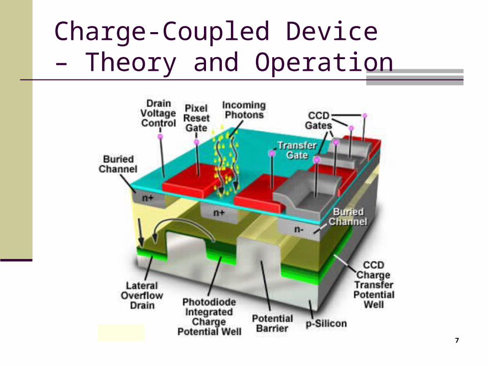
Charge-Coupled Device– Theory and Operation
8
Charge-Coupled Device– Architectures
Common types of CCD in use:
a) Full-Frame transfer or frame transfer devices
Use MOS photo-capacitors as detectors
b) Interline transfer devices
Use photodiodes and photo-capacitors as
detector.
9
Charge-Coupled Device – Full-Frame CCD Architecture All photodiodes in the pixel array act as image plane for
detecting photons during exposure period. Upon exposure of image, photons are collected by pixel
elements and converted into electrical potential. Each pixel, consists of four photodiodes masked with RGB
colored filters and contains portion of image. Readout of image by shifting rows of image, one row at a time
to shifter register. Shift register sequentially shifts row of image information to
output amplifier as a serial data stream All rows of image data are directed to output amplifier and
converted to digital data by ADC IC.
10
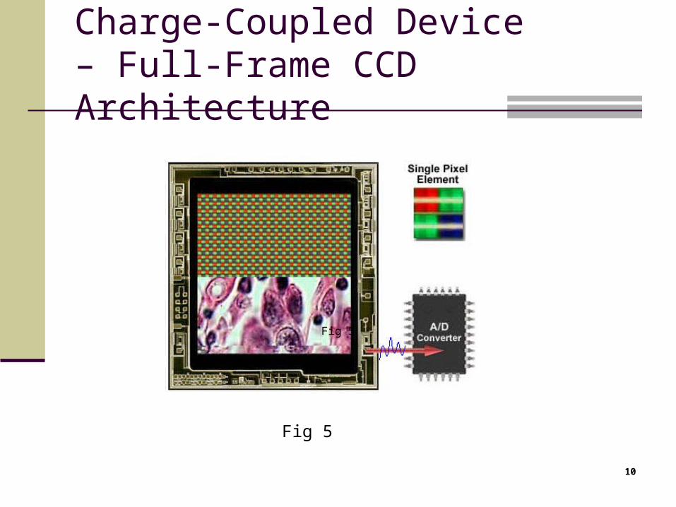
Charge-Coupled Device – Full-Frame CCD Architecture
Fig 5
Fig 5
11
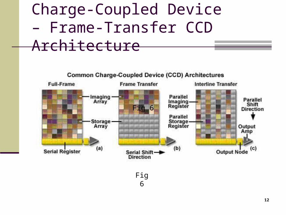
Charge-Coupled Device – Frame-Transfer CCD Architecture1. Similar to Full-Frame CCDs.
2. Two parallel register that divided into two separate areas, termed Image and Storage arrays.
3. Image plane consists of light-sensitive photodiode and act as incoming photons collector
4. Image data collected and converted to electrical signal in the image array.
5. Storage arrays not light sensitive as it use as to shift captured scene from image arrays
6. Following image exposure, charge accumulated in the photosensitive pixels is rapidly shifted to pixels on the storage side of the chip, typically within approximately 1 millisecond.
12
Charge-Coupled Device – Frame-Transfer CCD Architecture
Fig 6
Fig 6
13
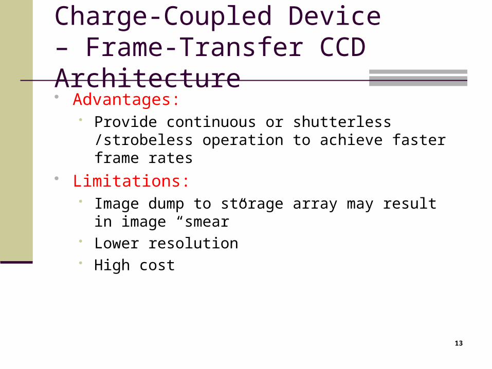
Charge-Coupled Device – Frame-Transfer CCD Architecture Advantages:
Provide continuous or shutterless /strobeless operation to achieve faster frame rates
Limitations: Image dump to storage array may result in image
“smear” Lower resolution High cost
14
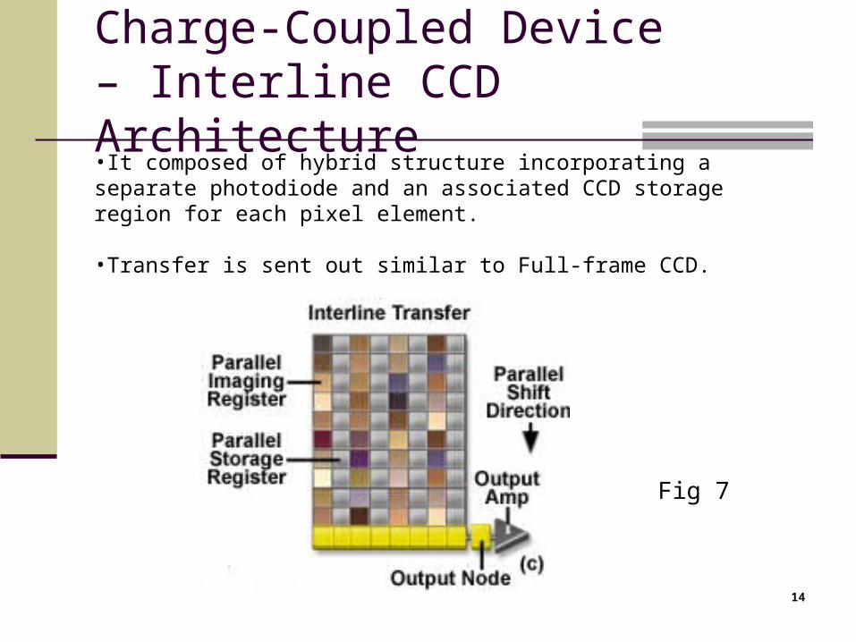
Charge-Coupled Device – Interline CCD Architecture
Fig 7
•It composed of hybrid structure incorporating a separate photodiode and an associated CCD storage region for each pixel element.
•Transfer is sent out similar to Full-frame CCD.
15
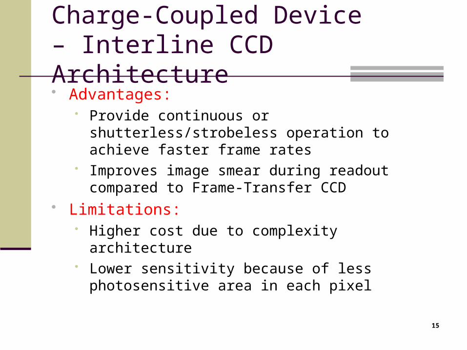
Charge-Coupled Device – Interline CCD Architecture Advantages:
Provide continuous or shutterless/strobeless operation to achieve faster frame rates
Improves image smear during readout compared to Frame-Transfer CCD
Limitations: Higher cost due to complexity architecture Lower sensitivity because of less photosensitive area
in each pixel
16
Charge-Coupled Device– Colour CCD Imaging Silicon based CCDs are monochrome in nature
No natural ability to determine varying of RGB information presented on pixel
Three techniques available for extracting of colour: Colour Sequential Three-Chip Colour Integral Colour Filter Arrays (CFA)
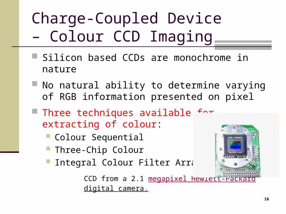
CCD from a 2.1 megapixel Hewlett-Packard digital camera.
17
Charge-Coupled Device– Colour CCD Imaging
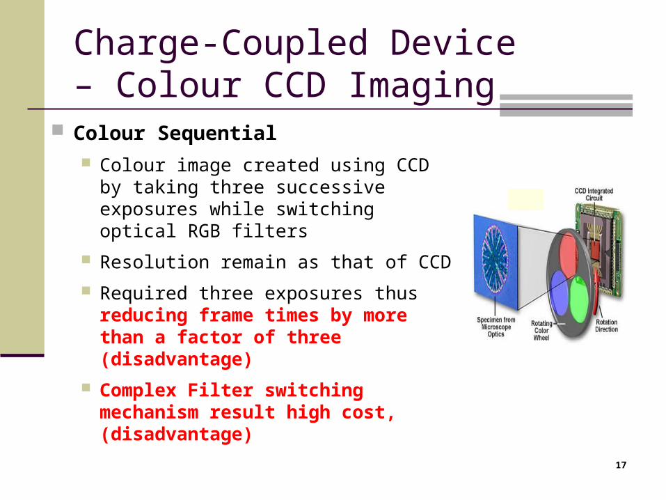
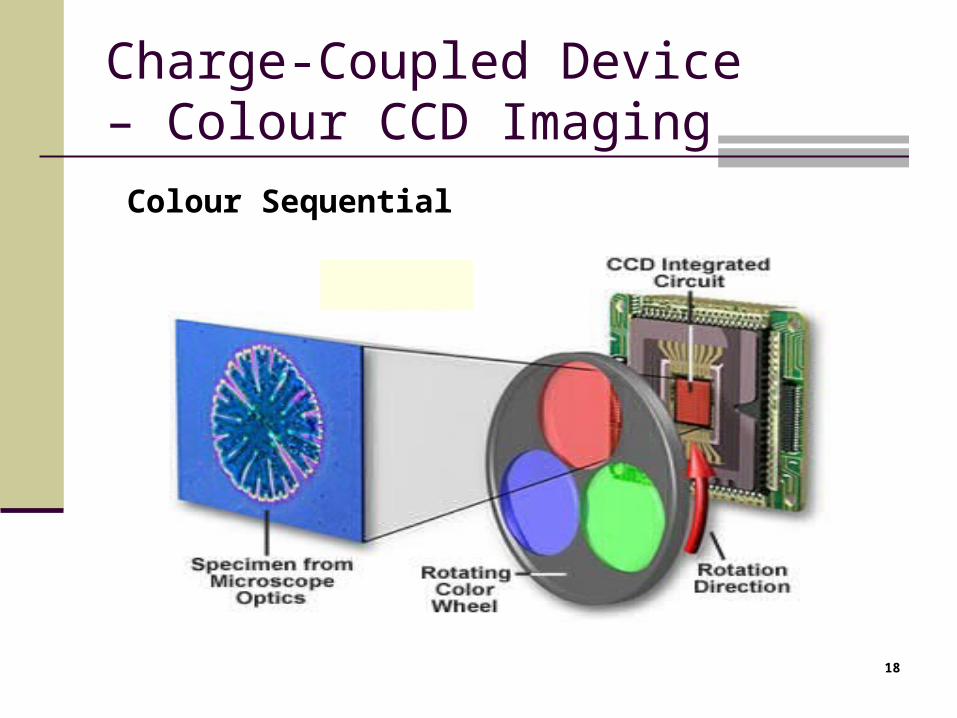
Colour Sequential Colour image created using CCD by
taking three successive exposures while switching optical RGB filters
Resolution remain as that of CCD
Required three exposures thus reducing frame times by more than a factor of three (disadvantage)
Complex Filter switching mechanism result high cost, (disadvantage)
18
Charge-Coupled Device– Colour CCD Imaging
Colour Sequential
19
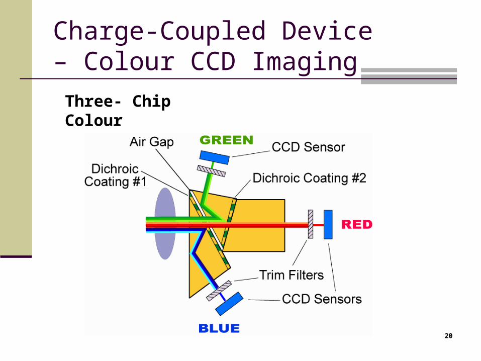
Charge-Coupled Device– Colour CCD Imaging Three-Chip Colour
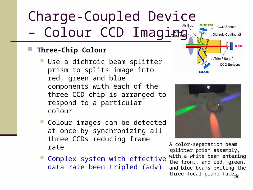
Use a dichroic beam splitter prism to splits image into red, green and blue components with each of the three CCD chip is arranged to respond to a particular colour
Colour images can be detected at once by synchronizing all three CCDs reducing frame rate
Complex system with effective data rate been tripled (adv) A color-separation beam splitter
prism assembly, with a white beam entering the front, and red, green, and blue beams exiting the three focal-plane faces.
20
Charge-Coupled Device– Colour CCD Imaging
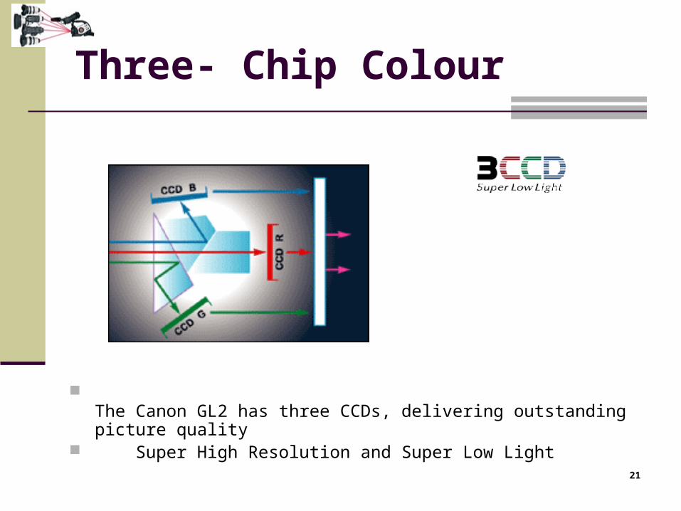
Three- Chip Colour
21
The Canon GL2 has three CCDs, delivering outstanding picture quality
Super High Resolution and Super Low Light
Three- Chip Colour
22
Charge-Coupled Device– Colour CCD Imaging
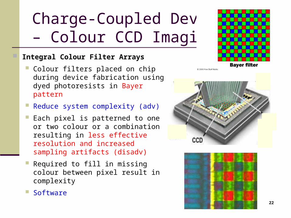
Integral Colour Filter Arrays
Colour filters placed on chip during device fabrication using dyed photoresists in Bayer pattern
Reduce system complexity (adv)
Each pixel is patterned to one or two colour or a combination resulting in less effective resolution and increased sampling artifacts (disadv)
Required to fill in missing colour between pixel result in complexity
Software
23
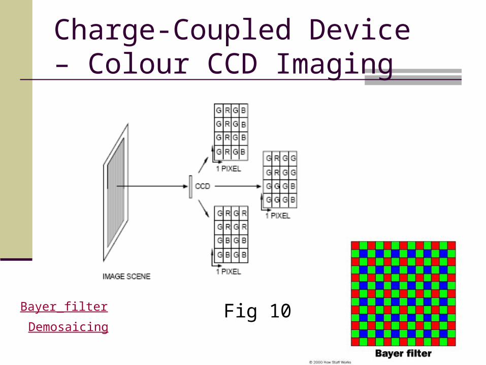
Fig 10
Charge-Coupled Device– Colour CCD Imaging
Bayer_filter
Demosaicing
24
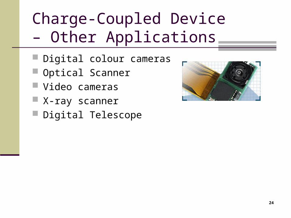
Charge-Coupled Device– Other Applications Digital colour cameras Optical Scanner Video cameras X-ray scanner Digital Telescope
25
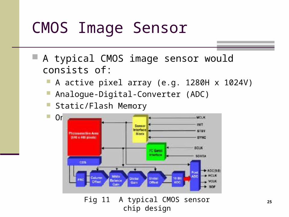
CMOS Image Sensor
A typical CMOS image sensor would consists of: A active pixel array (e.g. 1280H x 1024V) Analogue-Digital-Converter (ADC) Static/Flash Memory On-chip controller
Fig 11 A typical CMOS sensor chip design
26
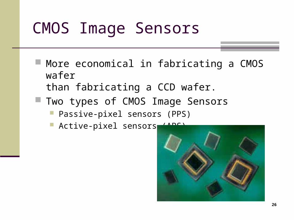
CMOS Image Sensors
More economical in fabricating a CMOS wafer than fabricating a CCD wafer.
Two types of CMOS Image Sensors Passive-pixel sensors (PPS) Active-pixel sensors (APS)
27
CMOS Image Sensors – Types of sensors
Passive-pixel sensors (PPS) First image-sensor devices used in the 1960s. A photosite converts photons (light) into an electrical
charge. Charge is carried off from the sensor and is amplified. Sensors are small—just large enough for the photosites
and their connections. Problem on these sensors is noise that appears as a
background pattern in the image. To cancel out this noise, sensors often use additional processing steps.
28
CMOS Image Sensors – Types of sensors Active-pixel sensors (APS)
most commonly used in cell phone cameras, web cameras and in some DSLRs.
has emerged as an alternative to CCD image sensors. Reduce the noise associated with passive-pixel
sensors. (adv) Active circuitry at each pixel determines its noise level
and cancel out.
29
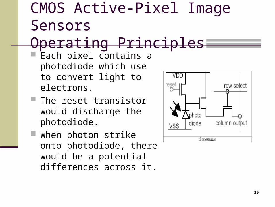
CMOS Active-Pixel Image SensorsOperating Principles Each pixel contains a
photodiode which use to convert light to electrons.
The reset transistor would discharge the photodiode.
When photon strike onto photodiode, there would be a potential differences across it.
30
CMOS Active-Pixel Image SensorsColour Operating Principles
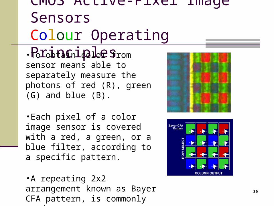
•To obtain color from sensor means able to separately measure the photons of red (R), green (G) and blue (B).
•Each pixel of a color image sensor is covered with a red, a green, or a blue filter, according to a specific pattern.
•A repeating 2x2 arrangement known as Bayer CFA pattern, is commonly used.
31
CMOS Active-Pixel Image SensorsColour Operating Principles When the image sensor is read out, line by
line, the pixel sequence comes out GRGRGR, follow by alternate line sequence is BGBGBG. This output is called sequential RGB (or sRGB).
Each pixel is sensitive only to one colour (one spectral band)
32
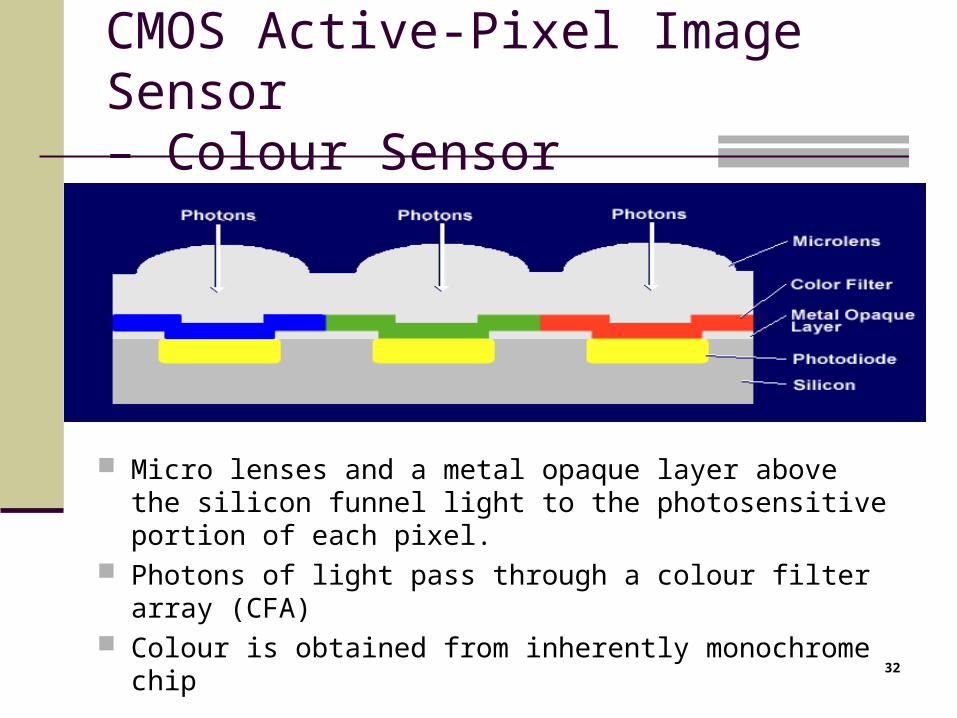
CMOS Active-Pixel Image Sensor – Colour Sensor
Micro lenses and a metal opaque layer above the silicon funnel light to the photosensitive portion of each pixel.
Photons of light pass through a colour filter array (CFA) Colour is obtained from inherently monochrome chip
33
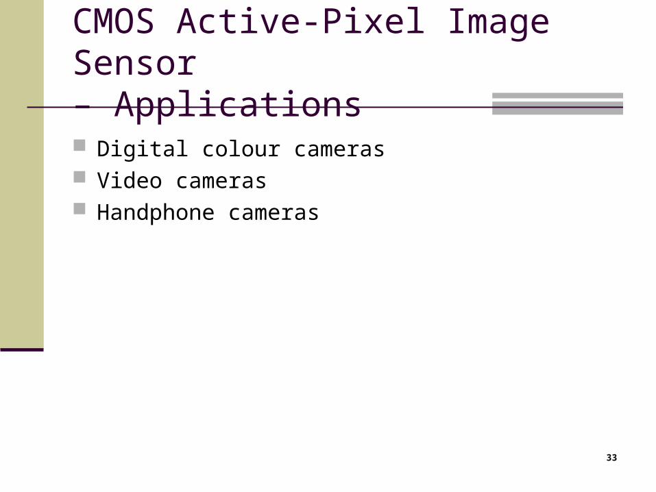
CMOS Active-Pixel Image Sensor– Applications
Digital colour cameras Video cameras Handphone cameras
34
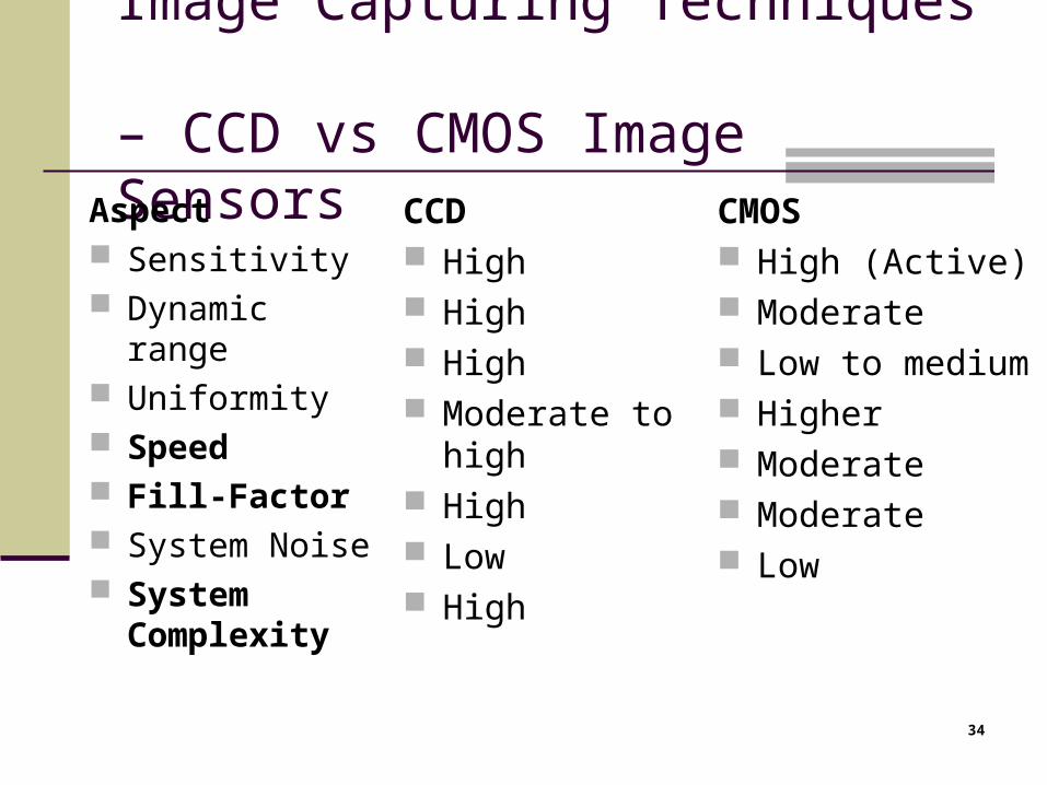
Image Capturing Techniques – CCD vs CMOS Image Sensors
Aspect Sensitivity Dynamic range Uniformity Speed Fill-Factor System Noise System
Complexity
CCD High High High Moderate to high High Low High
CMOS High (Active) Moderate Low to medium Higher Moderate Moderate Low
35
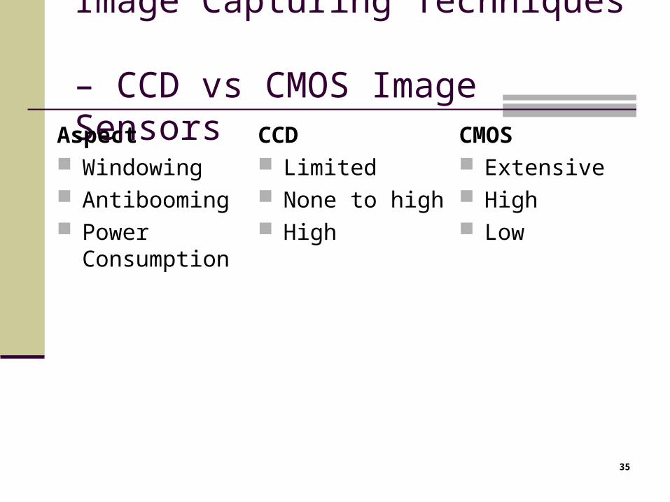
Image Capturing Techniques – CCD vs CMOS Image Sensors
Aspect Windowing Antibooming Power
Consumption
CCD Limited None to high High
CMOS Extensive High Low
36
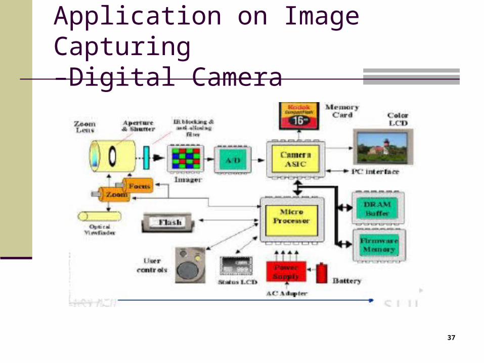
Application on Image Capturing –Digital Camera The basic concepts used by all digital cameras are
similar
Light is focus onto the plane (CCD) using the lens.
In 35mm cameras, the plane contains film, however, in the digital camera, the plane is occupied by the CCD
Images is processed out to the ADC via various methods depend on the type of CCD
Upon received digital signal from the ADC, DSP (digital signal processor) will generate images onto the display panel.
37
Application on Image Capturing –Digital Camera
38
Application on Image Capturing – Digital Camera Digital camera operational steps:
Exposure De-mosaicing White-balancing Colour correction Sharpening Compression File format
39
Application on Image Capturing – Digital Camera
40
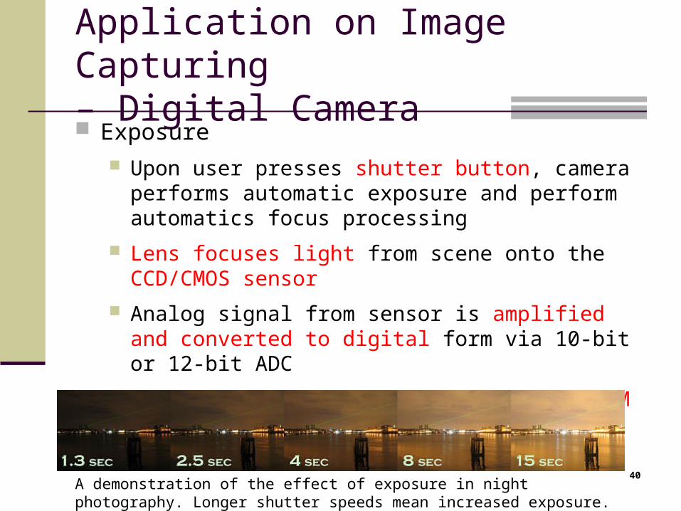
Application on Image Capturing – Digital Camera Exposure
Upon user presses shutter button, camera performs automatic exposure and perform automatics focus processing
Lens focuses light from scene onto the CCD/CMOS sensor
Analog signal from sensor is amplified and converted to digital form via 10-bit or 12-bit ADC
Image is then captured and stored in RAM
A demonstration of the effect of exposure in night photography. Longer shutter speeds mean increased exposure.
41
Application on Image Capturing – Digital Camera De-mosaicing
Digital Image data is processed by ASIC image processor (usually DSP)
Since a single colour image sensor which provides only one colour value for each light sensitive cell is used to determine pixel, an interpolation process is used to “fill in” missing colour for each pixel
Bayer_filter
Demosaicing
42
Application on Image Capturing – Digital Camera White balancing
A full colour image from de-mosaicing process is required to perform a white balancing for spectral variations for a perfect image by analyzing the scene and adjust red/blue signal to match the green signal in white and neutral area
Colour correction A digitalise colour correction is used to improve the
image after white balancing as image may appears as desaturated, muting bright colour due to RGB spectral sensitivities of sensor
43
Application on Image Capturing – Digital Camera Sharpening
Anti-aliasing filter and other lens components soften the captured image
An adaptive spatial filters process, which locate and emphasize fine edge detail in the image, is include in digital camera process to sharpen the image
44
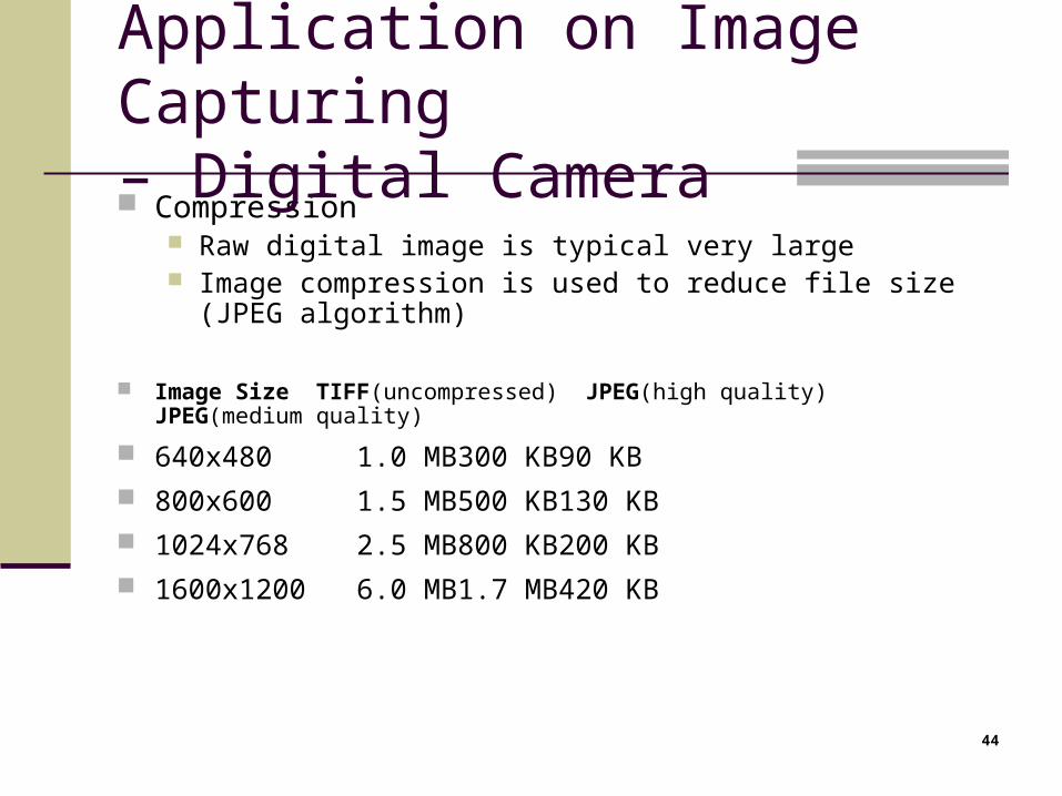
Compression Raw digital image is typical very large Image compression is used to reduce file size (JPEG
algorithm)
Image Size TIFF(uncompressed) JPEG(high quality) JPEG(medium quality)
640x480 1.0 MB 300 KB 90 KB
800x600 1.5 MB 500 KB 130 KB
1024x768 2.5 MB 800 KB 200 KB
1600x1200 6.0 MB 1.7 MB 420 KB
Application on Image Capturing – Digital Camera
45
Application on Image Capturing – Digital Camera File format
Compressed image data in a JPEG image file follow Exchangeable Image File (Exif) format
Image file also contains metadata: Camera manufacturer Model number Exact date and time of picture taken Focal length, subject distance, lens and shutter
speed used User-selected camera settings (sharpness
level, quality level, etc)
top ten digital camera
46
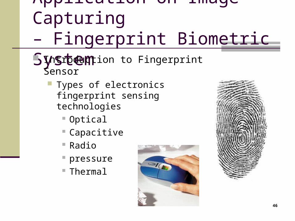
Application on Image Capturing – Fingerprint Biometric System Introduction to Fingerprint Sensor
Types of electronics fingerprint sensing technologies
Optical Capacitive Radio pressure Thermal
47
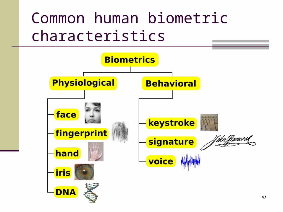
Common human biometric characteristics
48
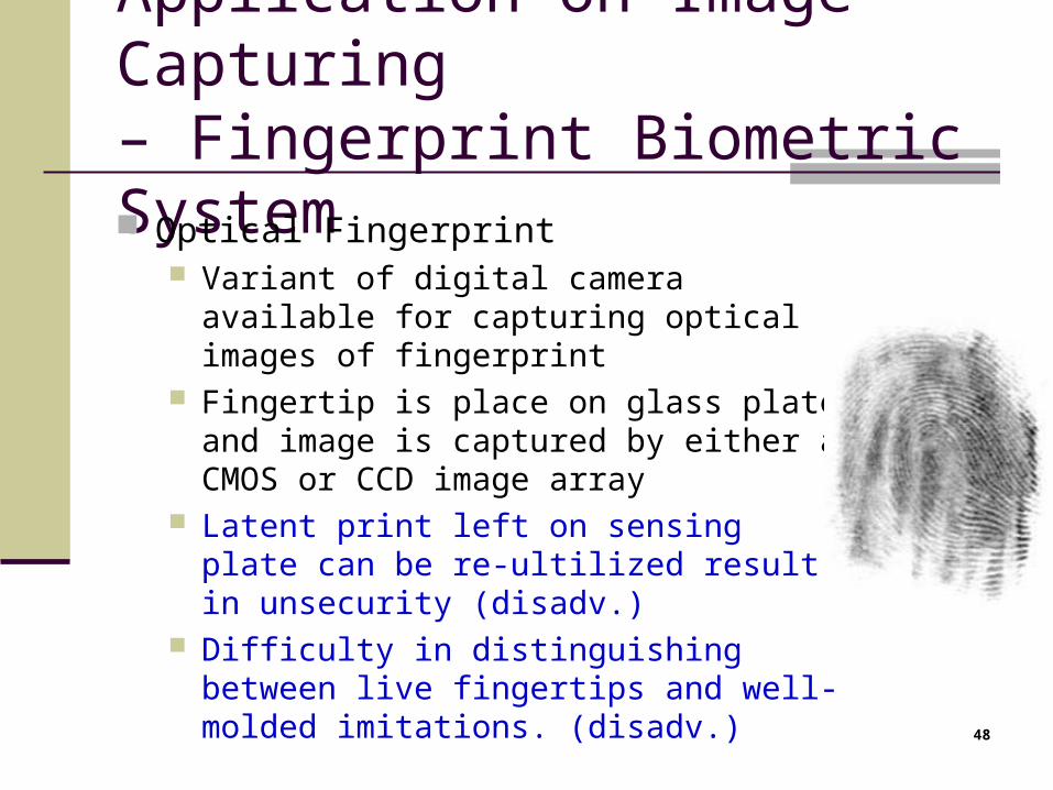
Application on Image Capturing – Fingerprint Biometric System Optical Fingerprint
Variant of digital camera available for capturing optical images of fingerprint
Fingertip is place on glass plate and image is captured by either a CMOS or CCD image array
Latent print left on sensing plate can be re-ultilized result in unsecurity (disadv.)
Difficulty in distinguishing between live fingertips and well-molded imitations. (disadv.)
49
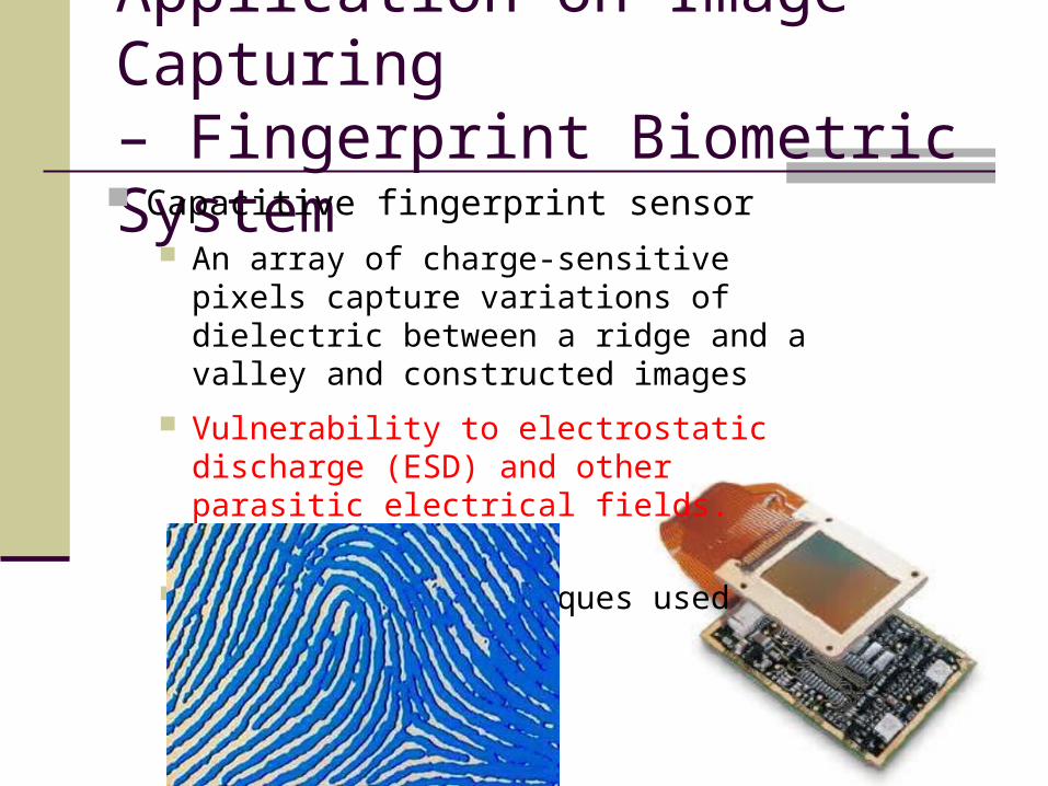
Application on Image Capturing – Fingerprint Biometric System Capacitive fingerprint sensor
An array of charge-sensitive pixels capture variations of dielectric between a ridge and a valley and constructed images
Vulnerability to electrostatic discharge (ESD) and other parasitic electrical fields. (disadv)
Most popular techniques used
50
Application on Image Capturing – Fingerprint Biometric System
51
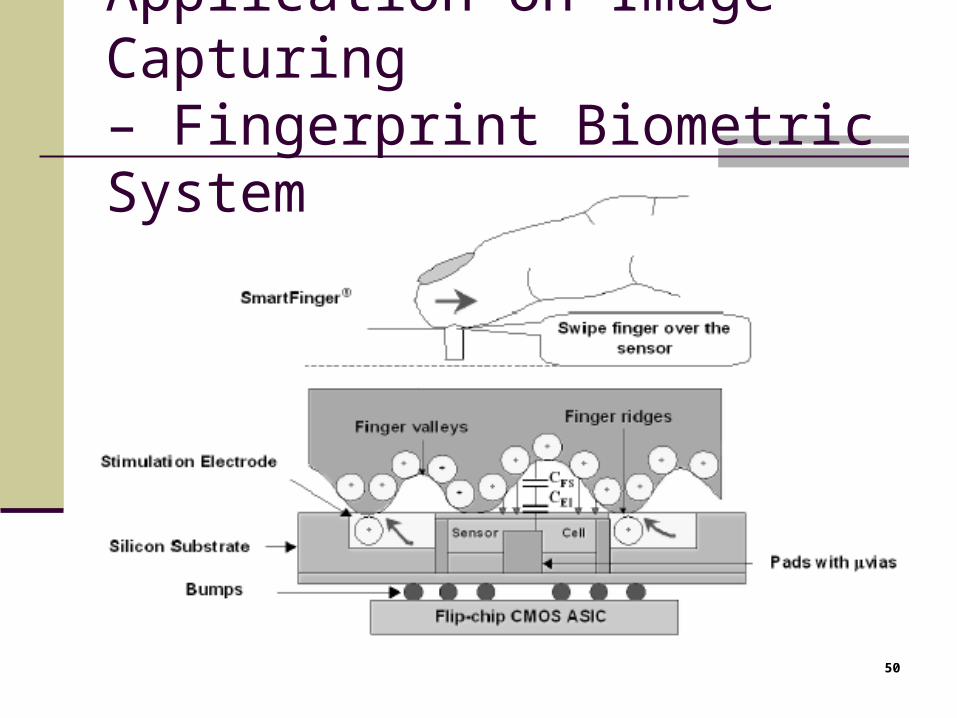
Application on Image Capturing – Fingerprint Biometric System Radio fingerprint sensor
A low-intensity radio wave energized by fingertip acts as a transmitter
Distance variation between ridges and valleys are detected by an array of suitably tuned antenna pixels
Require fingertip contact with emitting region of sensor
Difficult to deceive a radio sensor as it relies on physiological properties of skin (adv.)
Complexity sensor circuitry (disadv.)
52
Application on Image Capturing – Fingerprint Biometric System Pressure fingerprint sensor
A pressure-sensitive pixel array constructed from piezo-electric element which captures pattern of ridges in a fingerprint pressed against it.
Low sensitivity, inability to distinguish between real and fake fingertips, susceptibility to damage from excessive pressure (disadv)
53
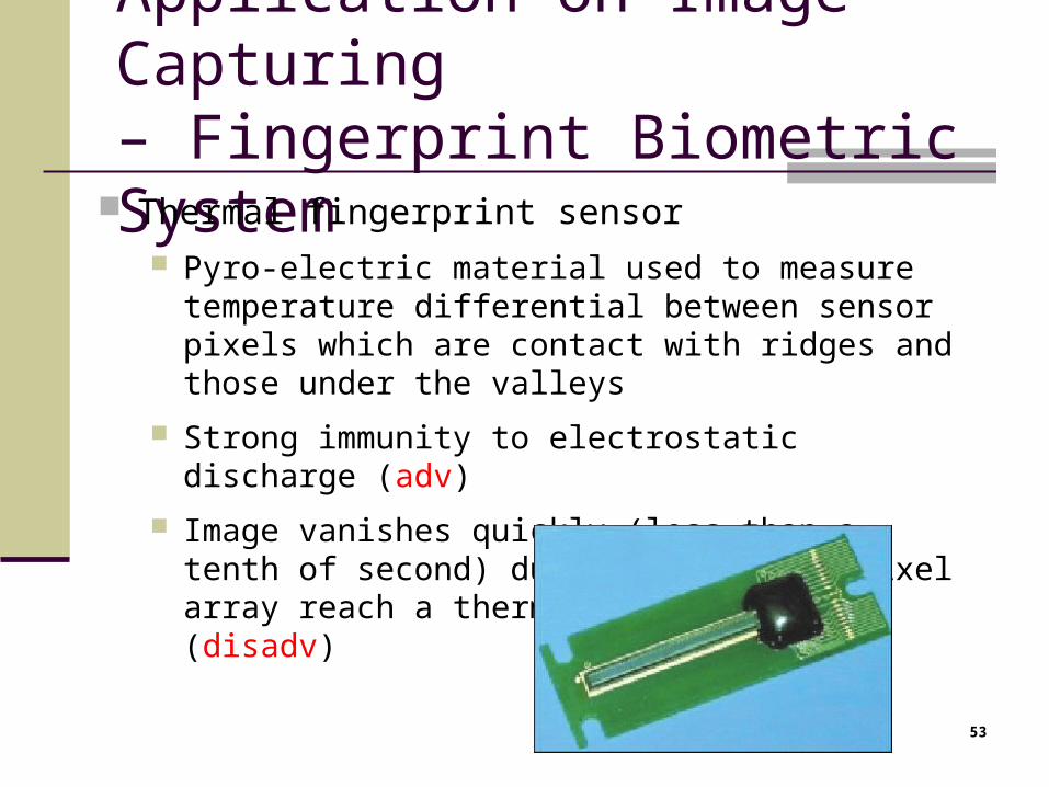
Application on Image Capturing – Fingerprint Biometric System
Thermal fingerprint sensor Pyro-electric material used to measure temperature
differential between sensor pixels which are contact with ridges and those under the valleys
Strong immunity to electrostatic discharge (adv)
Image vanishes quickly (less than a tenth of second) due to finger and pixel array reach a thermal equilibrium (disadv)
54
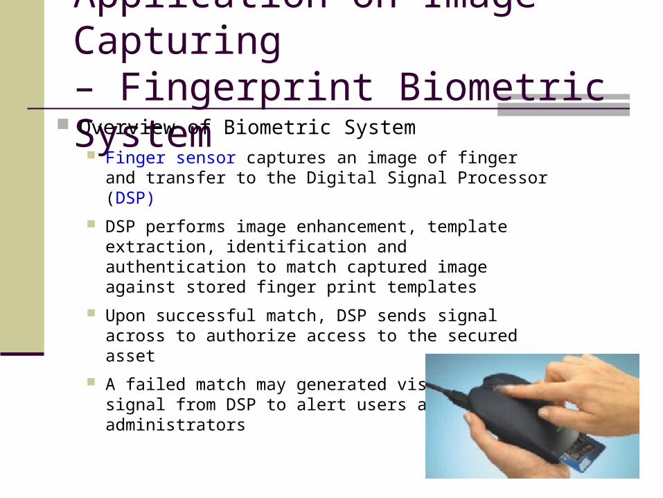
Application on Image Capturing – Fingerprint Biometric System
Overview of Biometric System Finger sensor captures an image of finger and transfer
to the Digital Signal Processor (DSP)
DSP performs image enhancement, template extraction, identification and authentication to match captured image against stored finger print templates
Upon successful match, DSP sends signal across to authorize access to the secured asset
A failed match may generated visual/audio signal from DSP to alert users and administrators

55
Advantages over other systems
Physical attributes are much harder to fake than identity cards.
You can't guess a fingerprint pattern like you can guess a password.
You can't misplace your fingerprints, irises or voice like you can misplace an access card.
You can't forget your fingerprints like you can forget a password.
SanDisk Secures USB Drive with Fingerprint ID Technology
56
Disadvantages
Optical scanners can't always distinguish between a picture of a finger and the finger itself, and
capacitive scanners can sometimes be fooled by a mold of a person's finger.
If somebody did gain access to an authorized user's prints, the person could trick the scanner.
In a worst-case scenario, a criminal could even cut off somebody's finger to get past a scanner security system.
Some scanners have additional pulse and heat sensors to verify that the finger is alive, rather than a mold or dismembered digit, but even these systems can be fooled by a gelatin print mold over a real finger.
57
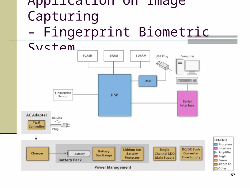
Application on Image Capturing – Fingerprint Biometric System
58
Application on Image Capturing – Fingerprint Biometric System Core subsystems of Fingerprint Biometric System
Digital Signal Processor capable of running high speed mathematically intensive Authentication (1:n) and Verification 1:1) fingerprint matching algorithms
Fingerprint Sensor capable of capturing distinguishing features of a fingerprint in digital format
External Memory for storing execution code and data/parameters such as fingerprint templates
RS232 Dual Channel/Receiver use to converts TIA/EIA-232-F inputs to 5V TTL/CMOS levels for interfacing across the RS232 standard
Power Management converts the input power from the AC adaptor or battery to the correct regulated voltages for various functional block
59
Review Questions
1. Name two types of image capturing technique used in the current market.
2. What is CCD? Briefly describe its operating principles.3. In a CCD module, the number of electrons collected at each
pixel is directly proportional to the light intensity and exposure time. (True / False)
4. Give two reasons why full-frame CCD is the most popular.5. Write down the three CCD colour imaging techniques.6. Which CCD colour imaging technique makes use of Bayer
filter?7. Which CCD colour imaging technique makes use of beam
splitter?8. Which CCD colour imaging technique makes use of rotating
RGB colour filter wheel?9. Name two applications using CCDs for image capturing.
60
Review Questions
10. Give two advantages of CMOS active-pixel sensors (APS) as compared to passive-pixel sensors (PPS).
11. CMOS Active-Pixel Image Sensor makes use of Bayer Colour Filter Array (CFA) to capture colour.
(True / False)12. List two applications using CMOS Active-Pixel
Image Sensor.13. Which type of image sensor has emerged as an
alternative to charge-coupled device (CCD) image sensors?
14. Which type of image compression technique is used in digital camera?
15. Name three types of electronic fingerprint sensors.
61
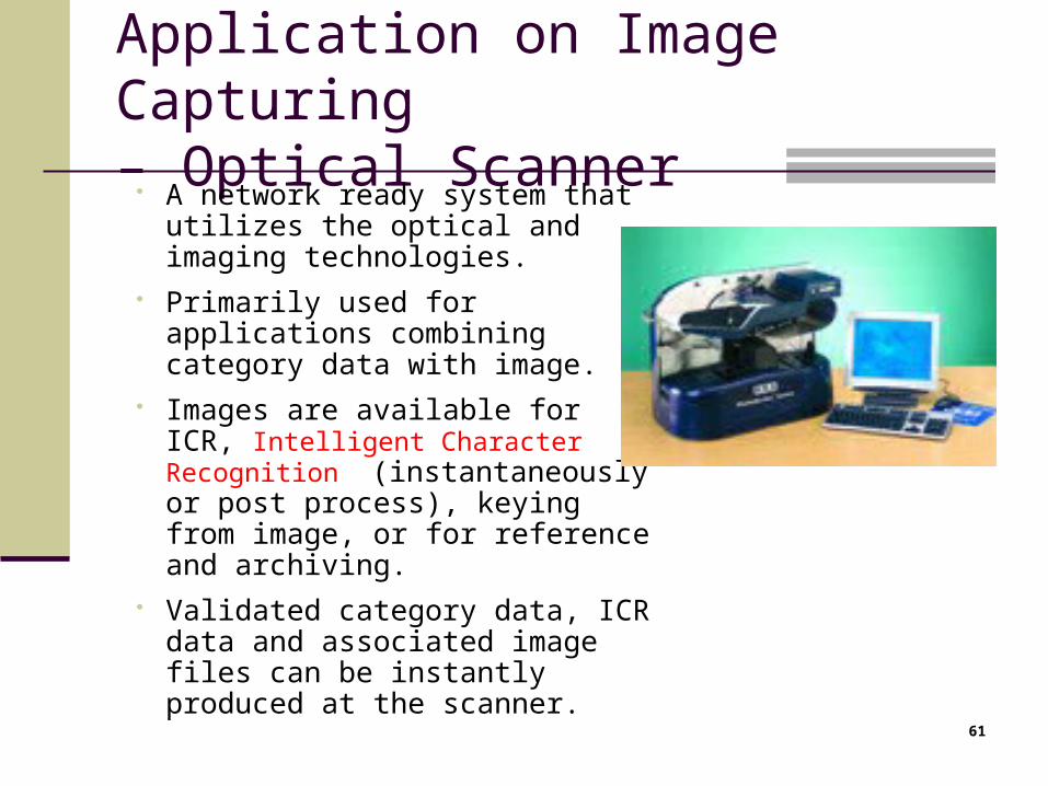
Application on Image Capturing – Optical Scanner
A network ready system that utilizes the optical and imaging technologies.
Primarily used for applications combining category data with image.
Images are available for ICR, Intelligent Character Recognition (instantaneously or post process), keying from image, or for reference and archiving.
Validated category data, ICR data and associated image files can be instantly produced at the scanner.
62
Image Capturing Techniques – CCD vs CMOS Image Sensors CCDs have a 100% fill factor but CMOS cameras
have much less.
CMOS sensors have a higher noise level than CCDs
Processing time for CCD is higher than CMOS sensors as CCD sensors use digital signal processing (DSP) to reduce or eliminate the noise.
63
Summary
Types of image capturing technique: Contact Image Sensor Charge-Coupled Device CMOS Image Sensor
Operating principles of each image capturing technique
Applications Charge-Coupled Device vs CMOS Image
Sensor