Embed Size (px)
Citation preview
1
Bandwidth Extension in CMOS with
Optimized On-Chip Inductors
Sunderarajan S. Mohan, Maria del Mar Hershenson, Stephen P. Boyd and
Thomas H. Lee
Correspondence Address:
Sunderarajan S. Mohan
CIS-029
Stanford University
Stanford, CA 94305-4070Phone: (650) 723-3658FAX: (650) 725-3383
E-Mail: [email protected]
The authors are with the Electrical Engineering Department, Stanford University, Stanford, CA 94305.
2
Abstract
We present a technique for enhancing the bandwidth of gigahertz broadband circuitry by using optimized
on-chip spiral inductors as shunt-peaking elements. The series resistance of the on-chip inductor is incor-
porated as part of the load resistance to permit a large inductance to be realized with minimum area and
capacitance. Simple, accurate inductance expressions are used in a lumped circuit inductor model to allow
the passive and active components in the circuit to be simultaneously optimized. A quick and efficient global
optimization method, based on geometric programming is discussed. The bandwidth extension technique
is applied in the implementation of a 2.125Gbaud preamplifier that employs a common-gate input stage
followed by a cascoded common-source stage. On-chip shunt-peaking is introduced at the dominant pole
to improve the overall system performance, including a 40% increase in the transimpedance. This imple-
mentation achieves a 1.6kΩ transimpedance and a 0.6µA input referred current noise, while operating with
a photodiode capacitance of 0.6pF. A fully differential topology ensures good substrate and supply noise
immunity. The amplifier, implemented in a triple metal, single poly, 14GHz fTmax , 0.5µm CMOS process,
dissipates 225mW of which 110mW is consumed by the 50Ω output driver stage. The optimized on-chip
inductors consume only 15% of the total area of 0.6mm2.
3
I. Introduction
TH e explosive growth in the commercial wired telecommunications market has generated tremendous
interest in low-cost implementations of radio frequency broad band receivers. The performance of such
a receiver’s front-end is determined to a large extent by the preamplifier. Traditionally, this preamplifier
has been fabricated in expensive GaAs and silicon bipolar technologies. However the quest for low cost so-
lutions in the commercial market has spurred a desire to implement RF-ICs in standard CMOS technology.
An additional advantage of these CMOS processes is that they permit the integration of the analog and
digital components, the holy grail for “system-on-chip” solutions. The performance of CMOS technologies
are improving constantly and consistently, thanks to the scaling achieved by the highly competitive mi-
croprocessor market. In fact, sub-micron CMOS technologies now exhibit sufficient performance for radio
frequency applications in the 1− 2GHz range. This paper discusses how optimized on-chip inductors can be
used to enhance the bandwidth of broad band amplifiers and thereby push the performance limits of CMOS
implementations. An attractive feature of this technique is that the bandwidth enhancement comes with no
additional power dissipation.
This bandwidth enhancement is achieved by shunt-peaking, a method first used in the 1940s to extend
the bandwidth of television tubes. Section II describes the fundamentals of this approach and then focuses
on how shunt-peaked amplifiers can be implemented in the integrated circuit environment. A new design
methodology that permits a large inductance to be realized in a small area is discussed. Section III discusses
how on-chip spiral inductors may be modeled using lumped circuit elements. A current sheet based approach
is used to obtain simple, accurate expressions for the inductance so that all elements in the lumped model
have analytical expressions. Thus, this lumped model can be incorporated in to a standard circuit design
environment such as SPICE, thereby circumventing the inconvenient, iterative interface between an inductor
simulator and a circuit design tool.
Section IV introduces a simple and efficient CAD tool for designing inductor circuits. This tool is based
on geometric programming (GP), a special type of optimization problem for which very efficient global
optimization methods have been developed. This technique enables the designer to optimize passive and
active devices simultaneously. This feature allows a shunt-peaked amplifier with on-chip inductors to be
optimized directly from specifications.
Section V and VI illustrate how shunt-peaking is used to improve the performance of a transimpedance
preamplifier. A prototype preamplifier, intended for gigabit optical communication systems, is implemented
in a 0.5µm CMOS process. The use of on-chip shunt peaking permits a 40% increase in the transimpedance
with no additional power dissipation. The optimized on-chip inductors only consume 15% of the total chip
area.
Section VII summarizes the main contributions of this paper.

4
II. Shunt Peaking
Although inductors are commonly associated with narrowband circuits, they are useful in broadband
circuits as well. In this section, we study how an inductor can enhance the bandwidth of a broadband
amplifier.
A. Shunt-peaked Amplification
[Figure 1 about here.]
We consider the simple common source amplifier illustrated in figure 1(a). For simplicity, we assume that the
small signal frequency response of this amplifier is determined by a single dominant pole, which is determined
solely by the output load resistance, R, and the load capacitance, C (figure 1(b)):
vout
vin(ω) =
gmR
1 + jωRC. (1)
The introduction of an inductance, L, in series with the load resistance (figure 1(c)) transforms the frequency
response of this amplifier. Now, the system has two poles and a zero, with the zero being determined by the
L/R time constant, while the poles (which may or may not be complex) are dependent on the values of all
three components:
vout
vin(ω) =
gm(R + jωL)1 + jωRC − ω2LC
(2)
The enhancement in bandwidth can be intuitively understood by noting that the positive reactance of the
inductance is used to tune out part of the negative reactance of the capacitance.
The frequency response of this shunt peaked amplifier is characterized by the ratio of the L/R and RC
time constants. This ratio is denoted by m so that L = mR2C.
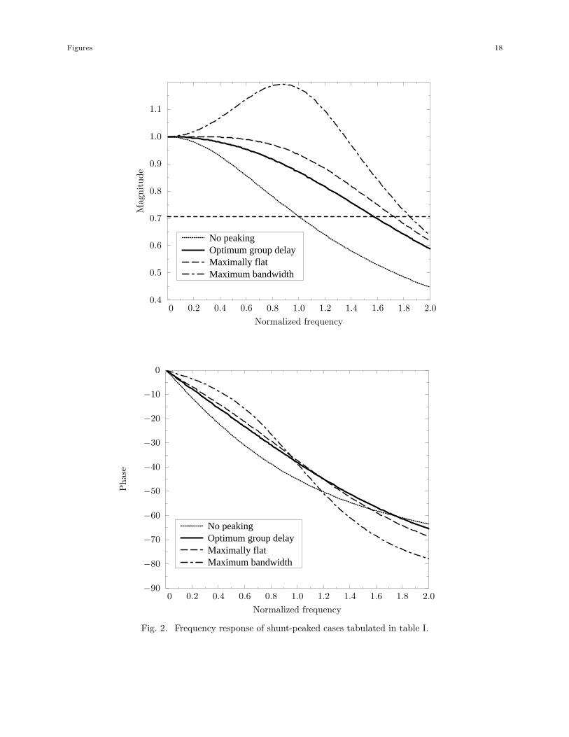
[Figure 2 about here.]
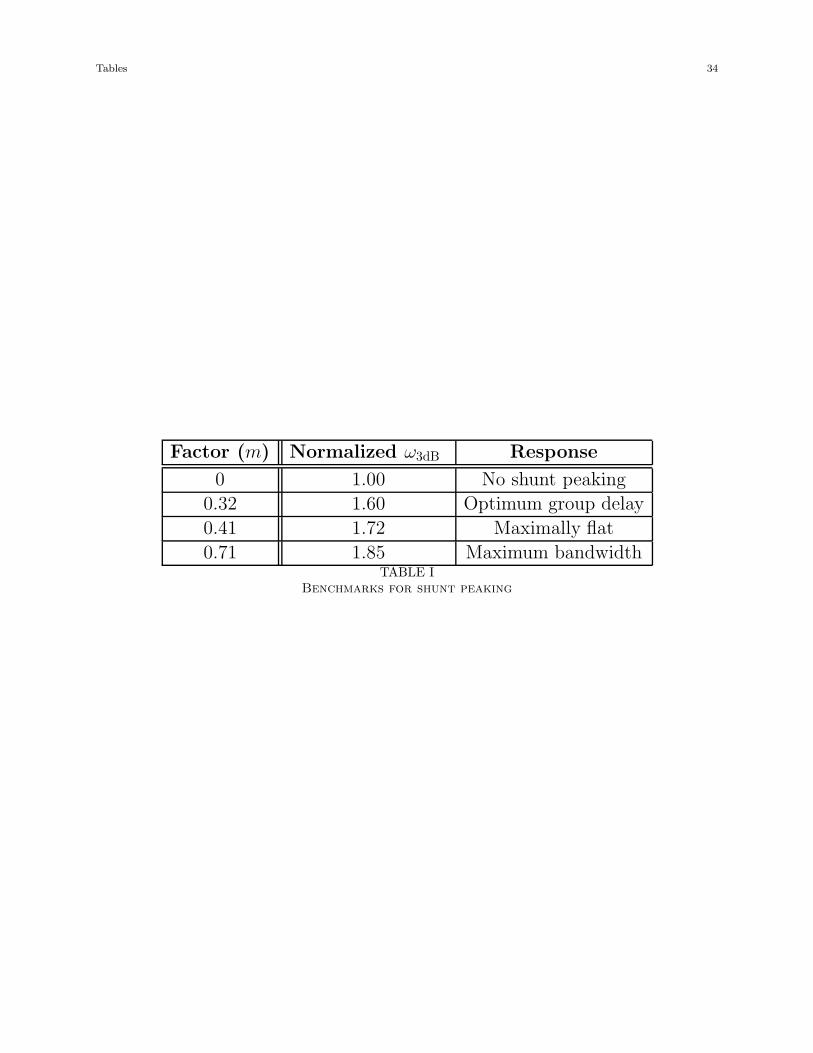
Figure 2 illustrates the frequency response of the shunt peaked amplifier for various values of m. The case
with no shunt peaking (m = 0) is used as the reference so that its low frequency gain and its ω3dB (3dB
bandwidth) are equal to one (RC = 1 and gmR = 1). The frequency response is plotted for the values of m
listed in table I [1].
[Table 1 about here.]
As expected, the 3dB bandwidth increases as m increases. The maximum bandwidth is obtained when
m = 0.71 and yields a 85% improvement in bandwidth. However, as can be clearly seen in the magnitude
plot, this comes at the cost of significant gain peaking. A maximally flat response may be obtained for
m = 0.41 with a still impressive bandwidth improvement of 72%.
Another interesting case occurs when m = 0.32. As seen in the phase plot, this best approximates a linear
phase response up to the 3dB bandwidth, which is 60% higher than the case without shunt peaking. This
case, called the ‘optimum group delay case’, is desirable for optimizing pulse fidelity in broadband systems
5
that transmit digital signals and is used in the prototype preamplifier described in sections V and VI.
B. On-Chip Shunt-Peaking
The non-idealities of on-chip inductors present several challenges for implementing monolithic gigahertz
circuitry. In shunt-peaking applications, the biggest issue is the the reduction in bandwidth improvement
because of the additional parasitic capacitance introduced by the on-chip inductor.
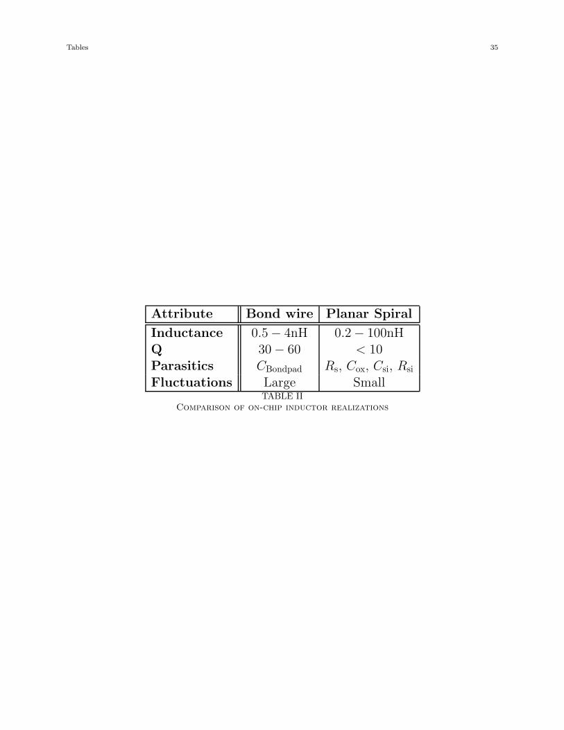
[Table 2 about here.]
On-chip inductors are usually realized using bond-wires or on-chip spirals. Table II compares the attributes
of these two implementations. Although bond wires exhibit much higher quality factors (Q) than spiral
inductors, their use is constrained by the limited range of realizable inductances and large production fluc-
tuations. Furthermore the bond-pad capacitance associated with the bond-wire can degrade performance.
This capacitance is typically ≈ 70 − 200fF, which is significant for gigahertz circuitry considering that the
maximum realizable inductance is only ≈ 4nH. Thus, although bond wires have been used as shunt-peaking
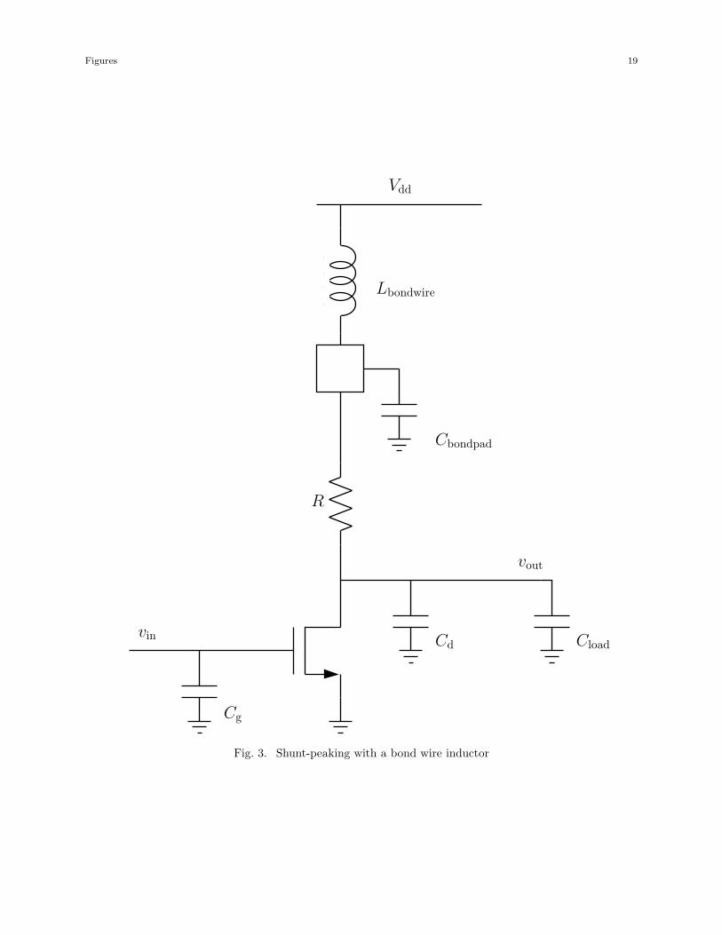
elements (figure 3), the net improvement in bandwidth is only ≈ 10% [2]. Furthermore, differential im-
plementations of shunt-peaked amplifiers experience a degradation in power supply rejection ratio (PSRR)
because of the inductance mismatch between the two bond wires.
[Figure 3 about here.]
On the other hand, spiral inductors exhibit good matching and are therefore suitable for differential
architectures. Furthermore, they permit a large range of inductances to be realized, albeit with smaller Q
values. We will now discuss a new design methodology that circumvents this limitation of low Q.
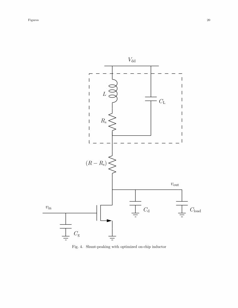
[Figure 4 about here.]
Figure 4 illustrates how the inductor Q can be made irrelevant by partitioning the total load resistance, R,
between the inductor’s series resistance (Rs) and the external resistance, which now takes on the value of
(R − Rs). Therefore, the inductor’s turn width, w, and spacing, s can be minimized to permit the desired
inductance to be realized while minimizing the spiral area and capacitance. The minimum w is now only
determined by current density considerations. The minimum turn spacing, s, is usually set by lithography
limitations.
The desired inductance is now a function of both the transistor’s and inductor’s parasitics as well as
the load capacitance and external resistance. Thus the optimization of on-chip shunt-peaking requires the
simultaneous optimization of passive and active components. This scenario accentuates the limitations of
using a field solver for modeling the inductor. Even if the field solver contains a general purpose optimization
routine, it serves no purpose as the performance parameters of the inductor (such as Q) alone cannot specify
the optimization goal. Therefore, several iterations would be needed (each requiring an interface between
the field solver and the circuit simulator), before an acceptable design can be obtained.
Therefore, a lumped circuit model with analytical expressions for all the elements in terms of the spiral’s
geometrical parameters and process process parameters is essential to facilitate circuit design and optimiza-

6
tion. The next section treats this subject in more detail.
III. Inductor Modeling
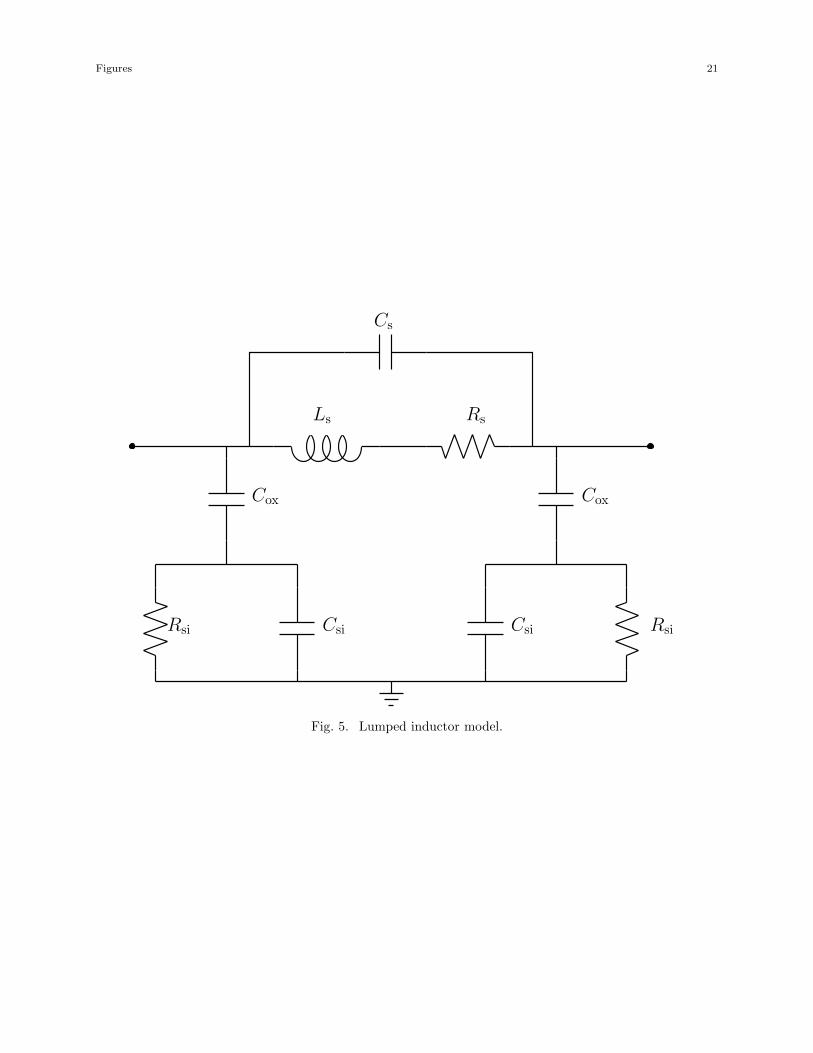
Significant work has gone into modeling spiral inductors using lumped circuit models [3], [4], [5], [6].
Figure 5 illustrates a commonly used model.
[Figure 5 about here.]
Although the parasitic resistors and capacitors in this model have simple physically intuitive expressions,
the inductance value itself lacks a simple, accurate expression. The inductance has typically been calculated
using the Greenhouse method [3], [7], [8]. Since this method operates by summing the self and mutual
inductances of the segments of the spiral using the method of moments, the complexity of the calculation
goes up as the square of the product or the number of sides and the number of turns. Thus, although
the Greenhouse method offers sufficient accuracy and adequate speed, it cannot provide an inductor design
directly from specifications, and is cumbersome for initial design.
A. Accurate Inductance Expressions
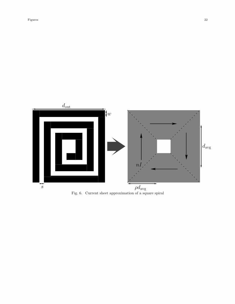
A simple and accurate expression for the inductance of a planar spiral can be obtained by approximating
the sides of the spirals by symmetrical current sheets with equivalent current densities( [9],[10] [11]).
[Figure 6 about here.]
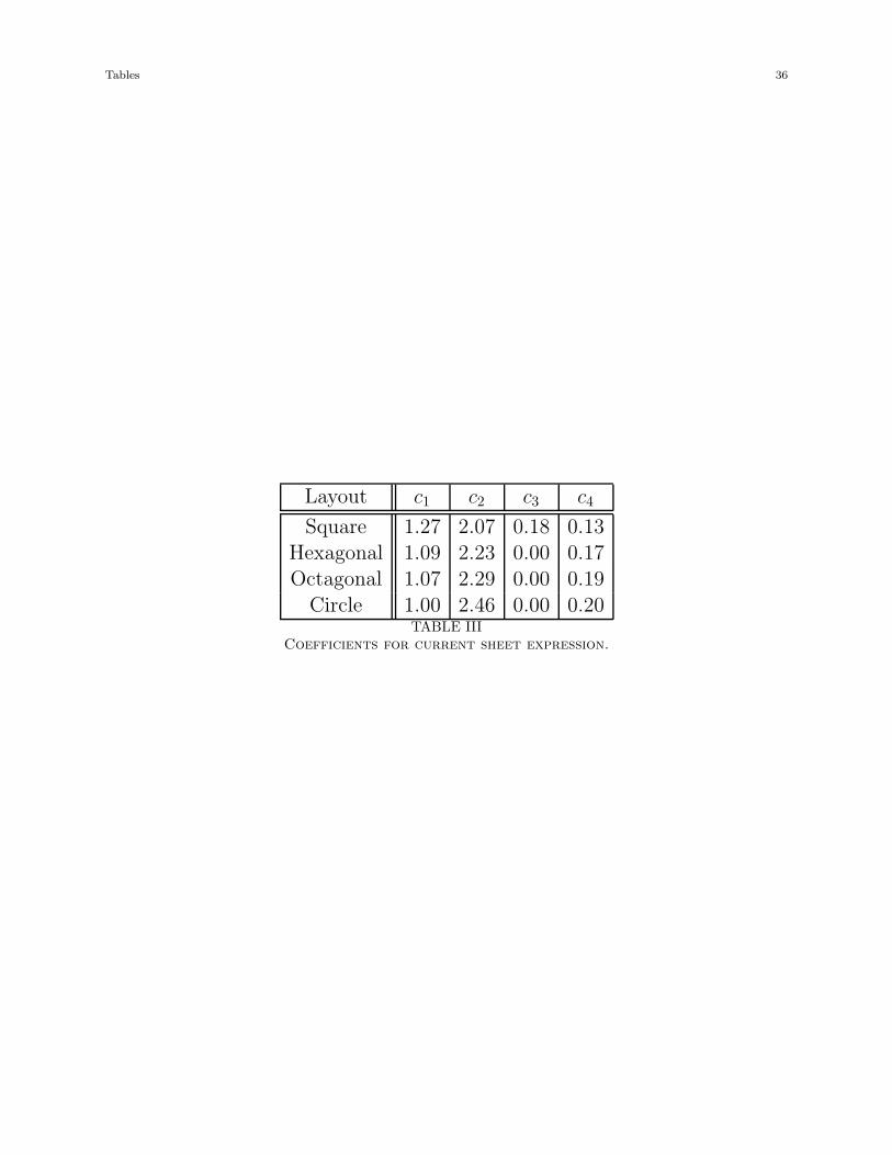
For example, in the case of the square as illustrated in figure 6, we obtain four identical current sheets:
the current sheets on opposite sides are parallel to one another, whereas the adjacent ones are orthogonal.
Using symmetry and the fact that sheets with orthogonal current sheets have zero mutual inductance, the
computation of the inductance is now reduced to evaluating the self inductance of one sheet and the mutual
inductance between opposite current sheets. These self and mutual inductances are evaluated using the
concepts of geometric mean distance (GMD), arithmetic mean distance (AMD) and arithmetic mean square
distance (AMSD)( [9], [12]). The resulting expression is:
Lgmd =µn2davgc1
2[ln(c2/ρ) + c3ρ + c4ρ
2], (3)
where davg is the average diameter of the spiral (which is the mean of the outer and inner diameters:
davg = 0.5(dout + din)) and ρ is a measure of how hollow or filled the spiral is (ρ = dout−dindout+din
). Thus a hollow
spiral has ρ closer to 0, while a filled spiral has ρ closer to 1. The coefficients ci are layout dependent and
are shown in Table III.
[Table 3 about here.]
Although the accuracy of this expressions worsens as the ratio s/w becomes large, it exhibits a maximum
error of 8% for s ≤ 3w [11]. Note that typical integrated spiral inductors are built with s ≤ w because
smaller spacing improves the inter-winding magnetic coupling and reduces the area consumed by the spiral.
A large spacing is only desired to reduce the inter-winding capacitance. In practice, this is not a concern as
7
this capacitance is dwarfed by the under-pass capacitance [3].
The simple, analytical nature of this expression makes it ideal for circuit design and optimization. When
combined with the lumped model shown in figure 5, it allows the designer to obtain design insight and
explore engineering trade-offs quickly and easily. Thus, field solvers are now only needed to verify the final
design.
IV. Optimization via geometric programming
This section presents an efficient method for the optimal design and synthesis of RF CMOS inductor
circuits. The method is based on geometric programming.
A. Geometric programming
Let f be a real-valued function of n real, positive variables x1, x2, . . . , xn. It is called a posynomial function
if it has the form
f(x1, . . . , xn) =t∑
k=1
ckxα1k1 xα2k
2 · · ·xαnkn
where cj ≥ 0 and αij ∈ R. When t = 1, f is called a monomial function. Thus, for example, 0.7 + 2x1/x23 +
x0.32 is posynomial and 2.3(x1/x2)1.5 is a monomial. Posynomials are closed under sums, products, and
nonnegative scaling.
A geometric program (GP) ) has the form
minimize f0(x)
subject to fi(x) ≤ 1, i = 1, 2, . . . , m,
gi(x) = 1, i = 1, 2, . . . , p,
xi > 0, i = 1, 2, . . . , n,
(4)
where fi are posynomial functions and gi are monomial functions. If f is a posynomial and g is a monomial,
then the constraint f(x) ≤ g(x) can be expressed as f(x)/g(x) ≤ 1 (since f/g is posynomial). From closure
under non-negativity, constraints of the form f(x) ≤ a, where a > 0 can also be used. Similarly, if g1 and g2
are both monomial functions, the constraint g1(x) = g2(x) can be expressed as g1(x)/g2(x) = 1 (since g1/g2
is monomial).
The key to solving GPs is a change of variables that converts the posynomial objective and constraint
functions into convex functions of the new variables. We define new variables yi = log xi, and take the
logarithm of a posynomial f to get
h(y) = log (f (ey1 , . . . , eyn)) = log
(t∑k
eaTk y+bk
)
where aTk = [α1k · · ·αnk] and bk = log ck. It can be shown that h is a convex function of y. This transfor-
8
mation converts the standard geometric program (4) into the convex optimization program:
minimize log f0(ey1 , . . . , eyn)
subject to log fi(ey1 , . . . , eyn) ≤ 0, i = 1, . . . , m
log gi(ey1 , . . . , eyn) = 0, i = 1, . . . , p,
(5)
which is called the convex form of the geometric program. Even though this problem is highly nonlinear, it
can be solved globally and very efficiently by recently developed interior-point methods (see, e.g., [14]).
For our purposes, the most important feature of geometric programs is that they can be globally solved
with great efficiency. GP solution algorithms also determine whether the problem is infeasible. Also, the
starting point for the optimization algorithm does not have any effect on the final solution; indeed, an initial
starting point or design is completely unnecessary.
B. Optimization of a Shunt-peaked Amplifier
Several circuit design problems may be posed as geometric programs [15], [16]. In particular, the design
specifications of inductor circuits can be formulated in a way suitable for geometric programming [17]. The
shunt-peaked amplifier design is a good example. As discussed earlier, in on-chip implementations, the series
resistance of the spiral inductor is absorbed within the gain resistor, R, and the capacitance of the inductor
Ctot is added to the load capacitance Cload. The goal is to minimize the capacitance added by the inductor
so that a large bandwidth extension can be obtained. The shunt-peaked amplifier problem can therefore be
written as the following geometric program:
minimize Ctank
subject to Ltank = mR2Ctank
w > wmin
Ctank ≥ Cload + Ctot
. . .
(6)
V. Design Example
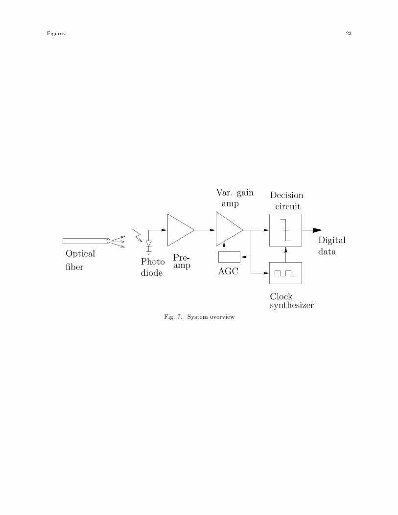
[Figure 7 about here.]
This section illustrates how optimized on-chip spiral inductors can improve the performance of a preamplifier
intended for the front-end of a gigabit optical system. Figure 7 shows the block diagram of a typical optical
communication receiver. The key performance parameters of such a front-end are bandwidth, sensitivity,
stability and dynamic range. The system’s bandwidth and sensitivity are determined largely by the pream-
plifier [18], [19], [20]. While a high bandwidth demands a small input resistance, good sensitivity requires
the resistors in the signal path to be large in order to minimize thermal noise. Thus, the preamplifier is
typically implemented using a transimpedance architecture as it provides a large bandwidth by synthesizing
a small input resistance using a much larger feedback resistor.
9
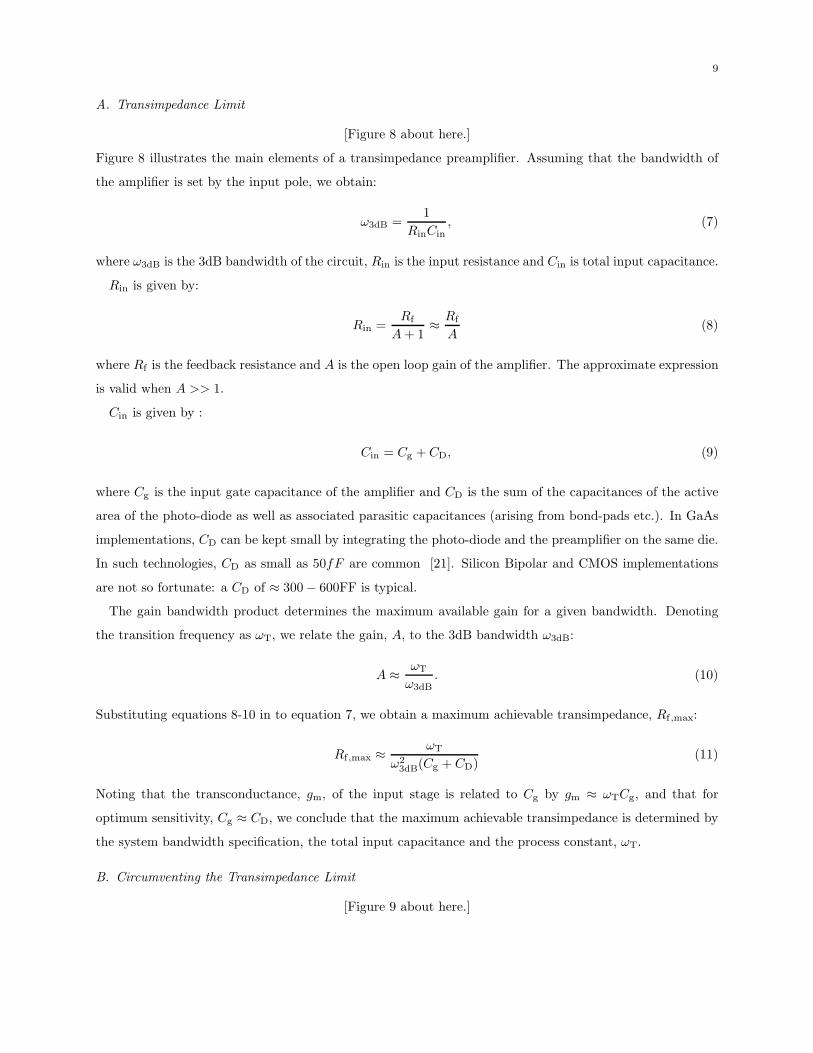
A. Transimpedance Limit
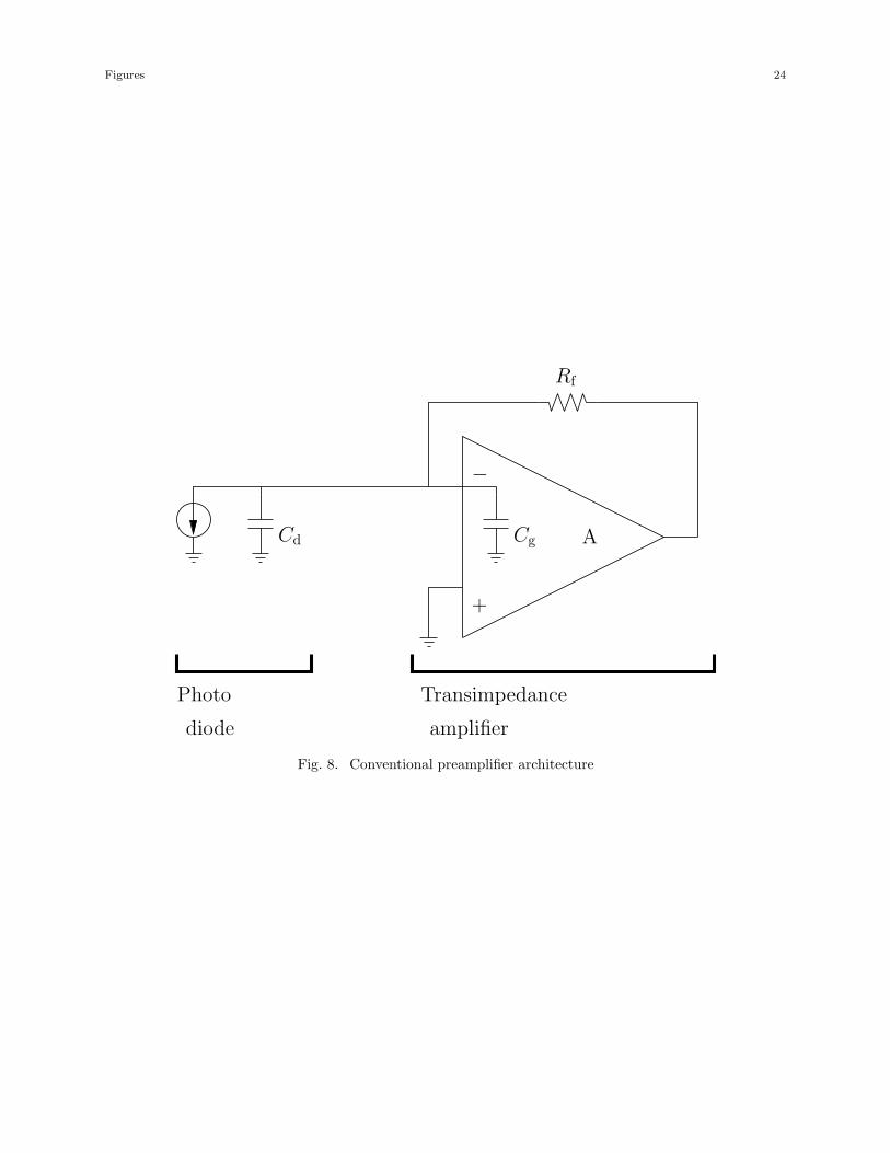
[Figure 8 about here.]
Figure 8 illustrates the main elements of a transimpedance preamplifier. Assuming that the bandwidth of
the amplifier is set by the input pole, we obtain:
ω3dB =1
RinCin, (7)
where ω3dB is the 3dB bandwidth of the circuit, Rin is the input resistance and Cin is total input capacitance.
Rin is given by:
Rin =Rf
A + 1≈ Rf
A(8)
where Rf is the feedback resistance and A is the open loop gain of the amplifier. The approximate expression
is valid when A >> 1.
Cin is given by :
Cin = Cg + CD, (9)
where Cg is the input gate capacitance of the amplifier and CD is the sum of the capacitances of the active
area of the photo-diode as well as associated parasitic capacitances (arising from bond-pads etc.). In GaAs
implementations, CD can be kept small by integrating the photo-diode and the preamplifier on the same die.
In such technologies, CD as small as 50fF are common [21]. Silicon Bipolar and CMOS implementations
are not so fortunate: a CD of ≈ 300 − 600FF is typical.
The gain bandwidth product determines the maximum available gain for a given bandwidth. Denoting
the transition frequency as ωT, we relate the gain, A, to the 3dB bandwidth ω3dB:
A ≈ ωT
ω3dB. (10)
Substituting equations 8-10 in to equation 7, we obtain a maximum achievable transimpedance, Rf,max:
Rf,max ≈ ωT
ω23dB(Cg + CD)
(11)
Noting that the transconductance, gm, of the input stage is related to Cg by gm ≈ ωTCg, and that for
optimum sensitivity, Cg ≈ CD, we conclude that the maximum achievable transimpedance is determined by
the system bandwidth specification, the total input capacitance and the process constant, ωT.
B. Circumventing the Transimpedance Limit
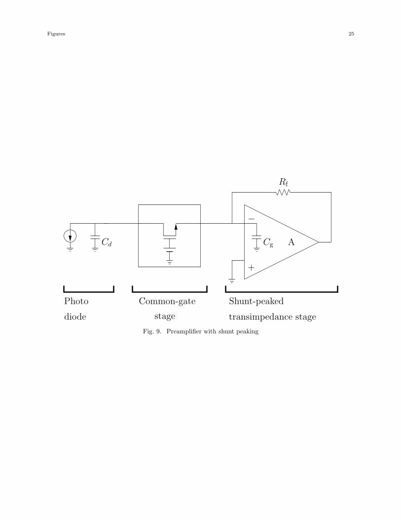
[Figure 9 about here.]
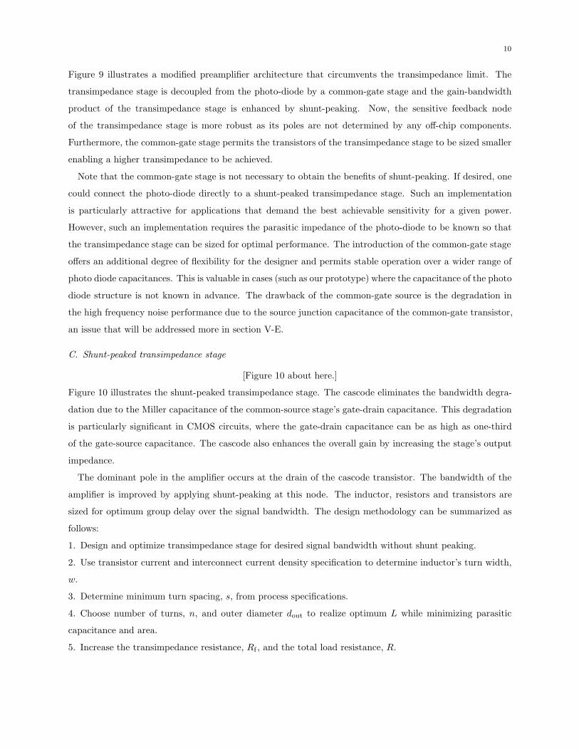
10
Figure 9 illustrates a modified preamplifier architecture that circumvents the transimpedance limit. The
transimpedance stage is decoupled from the photo-diode by a common-gate stage and the gain-bandwidth
product of the transimpedance stage is enhanced by shunt-peaking. Now, the sensitive feedback node
of the transimpedance stage is more robust as its poles are not determined by any off-chip components.
Furthermore, the common-gate stage permits the transistors of the transimpedance stage to be sized smaller
enabling a higher transimpedance to be achieved.
Note that the common-gate stage is not necessary to obtain the benefits of shunt-peaking. If desired, one
could connect the photo-diode directly to a shunt-peaked transimpedance stage. Such an implementation
is particularly attractive for applications that demand the best achievable sensitivity for a given power.
However, such an implementation requires the parasitic impedance of the photo-diode to be known so that
the transimpedance stage can be sized for optimal performance. The introduction of the common-gate stage
offers an additional degree of flexibility for the designer and permits stable operation over a wider range of
photo diode capacitances. This is valuable in cases (such as our prototype) where the capacitance of the photo
diode structure is not known in advance. The drawback of the common-gate source is the degradation in
the high frequency noise performance due to the source junction capacitance of the common-gate transistor,
an issue that will be addressed more in section V-E.
C. Shunt-peaked transimpedance stage
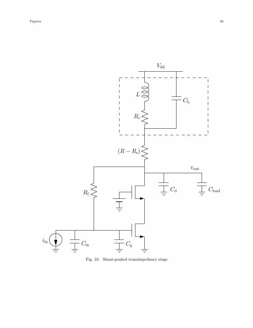
[Figure 10 about here.]
Figure 10 illustrates the shunt-peaked transimpedance stage. The cascode eliminates the bandwidth degra-
dation due to the Miller capacitance of the common-source stage’s gate-drain capacitance. This degradation
is particularly significant in CMOS circuits, where the gate-drain capacitance can be as high as one-third
of the gate-source capacitance. The cascode also enhances the overall gain by increasing the stage’s output
impedance.
The dominant pole in the amplifier occurs at the drain of the cascode transistor. The bandwidth of the
amplifier is improved by applying shunt-peaking at this node. The inductor, resistors and transistors are
sized for optimum group delay over the signal bandwidth. The design methodology can be summarized as
follows:
1. Design and optimize transimpedance stage for desired signal bandwidth without shunt peaking.
2. Use transistor current and interconnect current density specification to determine inductor’s turn width,
w.
3. Determine minimum turn spacing, s, from process specifications.
4. Choose number of turns, n, and outer diameter dout to realize optimum L while minimizing parasitic
capacitance and area.
5. Increase the transimpedance resistance, Rf , and the total load resistance, R.
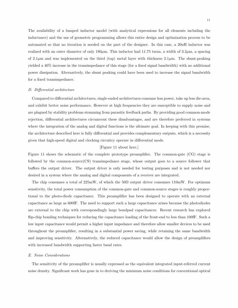
11
The availability of a lumped inductor model (with analytical expressions for all elements including the
inductance) and the use of geometric programming allows this entire design and optimization process to be
automated so that no iteration is needed on the part of the designer. In this case, a 20nH inductor was
realized with an outer diameter of only 180µm. This inductor had 11.75 turns, a width of 3.2µm, a spacing
of 2.1µm and was implemented on the third (top) metal layer with thickness 2.1µm. The shunt-peaking
yielded a 40% increase in the transimpedance of this stage (for a fixed signal bandwidth) with no additional
power dissipation. Alternatively, the shunt peaking could have been used to increase the signal bandwidth
for a fixed transimpedance.
D. Differential architecture
Compared to differential architectures, single-ended architectures consume less power, take up less die-area,
and exhibit better noise performance. However at high frequencies they are susceptible to supply noise and
are plagued by stability problems stemming from parasitic feedback paths. By providing good common-mode
rejection, differential architectures circumvent these disadvantages, and are therefore preferred in systems
where the integration of the analog and digital functions is the ultimate goal. In keeping with this premise,
the architecture described here is fully differential and provides complementary outputs, which is a necessity
given that high-speed digital and clocking circuitry operate in differential mode.
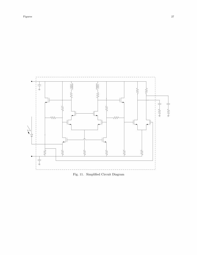
[Figure 11 about here.]
Figure 11 shows the schematic of the complete prototype preamplifier. The common-gate (CG) stage is
followed by the common-source(CS) transimpedance stage, whose output goes to a source follower that
buffers the output driver. The output driver is only needed for testing purposes and is not needed nor
desired in a system where the analog and digital components of a receiver are integrated.
The chip consumes a total of 225mW, of which the 50Ω output driver consumes 110mW. For optimum
sensitivity, the total power consumption of the common-gate and common-source stages is roughly propor-
tional to the photo-diode capacitance. This preamplifier has been designed to operate with an external
capacitance as large as 600fF. The need to support such a large capacitance arises because the photodiodes
are external to the chip with correspondingly large bondpad capacitances. Recent research has explored
flip-chip bonding techniques for reducing the capacitance loading of the front-end to less than 100fF. Such a
low input capacitance would permit a higher input impedance and therefore allow smaller devices to be used
throughout the preamplifier, resulting in a substantial power saving, while retaining the same bandwidth
and improving sensitivity. Alternatively, the reduced capacitance would allow the design of preamplifiers
with increased bandwidth supporting faster baud rates.
E. Noise Considerations
The sensitivity of the preamplifier is usually expressed as the equivalent integrated input-referred current
noise density. Significant work has gone in to deriving the minimum noise conditions for conventional optical
12
preamplifiers [18], [22]. Some studies have also investigated how inductors can increase the sensitivity of
optical preamplifiers implemented in GaAs [19].
The noise performance of the common-gate(CG) input stage followed by the common-source (CG) tran-
simpedance stage has been studied in GaAs HBT and BiCMOS processes [23]. Although, a simulation
involving a single-ended CMOS version was reported, it ignored the effects of the source and drain junction
capacitances and did not consider the impact of short-channel effects on small signal behavior and noise [24].
Junction capacitances in sub-micron CMOS processes are comparable to the gate capacitances and there-
fore significantly influence both noise behavior and bandwidth. A rigorous analysis that includes the impact
of the junction capacitances and short-channel behavior yields two conditions for a noise optimum. First,
the saturation mode gate capacitance of the common-source stage must equal the saturation mode drain
capacitance of the common-gate stage so that Cgs,CS + Cgd,CS = Cgd,CG + Cdb,CG. Second, the saturation
mode input capacitance of the common-gate stage (which is the gate-source capacitance, Cgs,CG, plus the
source-substrate capacitance Csb,CG) must equal βCext, where β ≈ 0.8 − 1. β is a function of both devices’
ωT, their coefficients of channel thermal noise (γ), and their ratios of junction capacitance to gate capac-
itance, all of which are bias dependent. For a typical CMOS device in saturation, (Cgs + Csb) is around
3-4 times as big as (Cgd + Cdb) and therefore the common-source stage can now be sized smaller, allowing
a corresponding increase in the feedback resistance and a dramatic decrease in power consumption, while
retaining the same device fT . The buffer stage that follows the common-source stage can also be sized
smaller, as can the width of all the interconnects, resulting in a smaller die area. The transconductance
of the common-gate stage only needs to be large enough to ensure that the input pole is non-dominant,
enabling the power consumption of the first stage to be small.
The introduction of the common-gate stage introduces three new noise sources: the thermal noise of the
source resistor, the thermal noise of the drain resistor, and the thermal channel noise of the common-gate
transistor. Of these terms, careful design ensures that the resistors are made large enough so as not to
significantly affect the noise performance. The thermal channel noises of the the common-gate and common-
source devices are reflected at the input by equivalent current noise spectral densities proportional to the
square of the frequency. When integrated over frequency, these terms dominate, a behavior typical of short-
channel CMOS processes, where carrier velocity saturation conditions cause thermal channel noise to increase
due to excess noise stemming from hot electron effects [25]. The upside is that the continuing reduction in
gate length promises higher fT CMOS devices, thereby improving noise performance. However, carrier
velocity saturation causes the small signal transconductance (and fT ) to be smaller than that predicted by
long channel (square-law) approximations.
VI. Layout and Experimental Details
[Figure 12 about here.]
As shown in the die photo (figure 12), the chip area is dominated by the passive components, which is
13
typical of RF-ICs. However, the two inductors combine for less than 15% of the total area, thanks to
the optimized shunt-peaking technique described in the earlier sections. A patterned ground shield is used
beneath the inductors to reduce substrate coupling [26]. Differential symmetry and cross quad layout are
used to ensure maximum matching, thereby reducing common-mode noise and systematic offset. 16pF of
on chip capacitance is used to provide supply decoupling. Several substrate contacts, placed around the
transistors, minimize source inductance. The floor plan keeps the sensitive input bond pads as far away from
the other pads as possible.
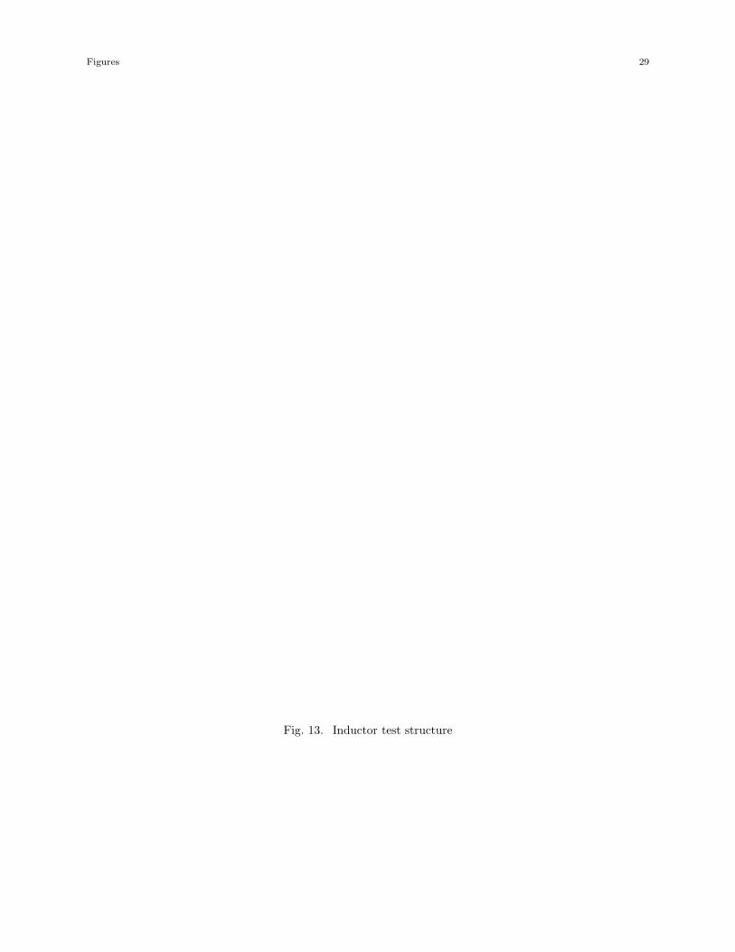
[Figure 13 about here.]
Figure 13 shows the test structure of the spiral inductor used for shunt-peaking. The S-parameters of
the inductor were measured using coplanar ground-signal-ground (GSG) probes and an open calibration
structure. The inductance and the one-port impedance (which is the relevant measure in our amplifier) were
extracted from these measurements.
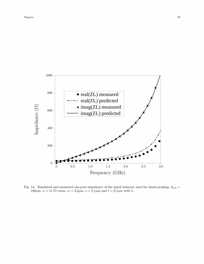
[Figure 14 about here.]
As shown in figure 14, good agreement between the prediction of the lumped circuit inductor model and
measured data is obtained for the equivalent one-port impedance of the spiral inductor used for shunt-
peaking. In particular, we note that the measured inductance of 20.5nH matches the 20.3nH value predicted
by our simple inductance expressions to within a 1% error.
Figure 15 shows the preamplifier’s simulated transimpedance versus frequency for photodiode capacitances
varying from 100fF to 700fF. As can be seen, the 3dB bandwidth is around 1.2GHz and only weakly
dependent on the photodiode capacitance. Maximum gain peaking is 1dB. These simulations are run with
the output driving a 50Ω resistance and 1pF capacitance.
[Figure 15 about here.]
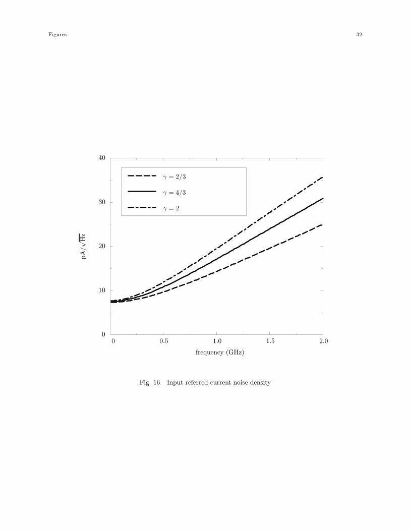
Figure 16 illustrates the preamplifier’s simulated equivalent input referred current noise spectral density
for a photodiode capacitance of 600fF. The coefficient of channel thermal noise (γ) is varied from 2/3, the
long-channel value, to 2, to discern the degradation in sensitivity due to excess noise in short channel devices.
The worst case value of 2 predicts an input referred current noise of 0.6µA, a significant degradation from
the 0.4µA predicted by long-channel estimates.
[Figure 16 about here.]
[Figure 17 about here.]
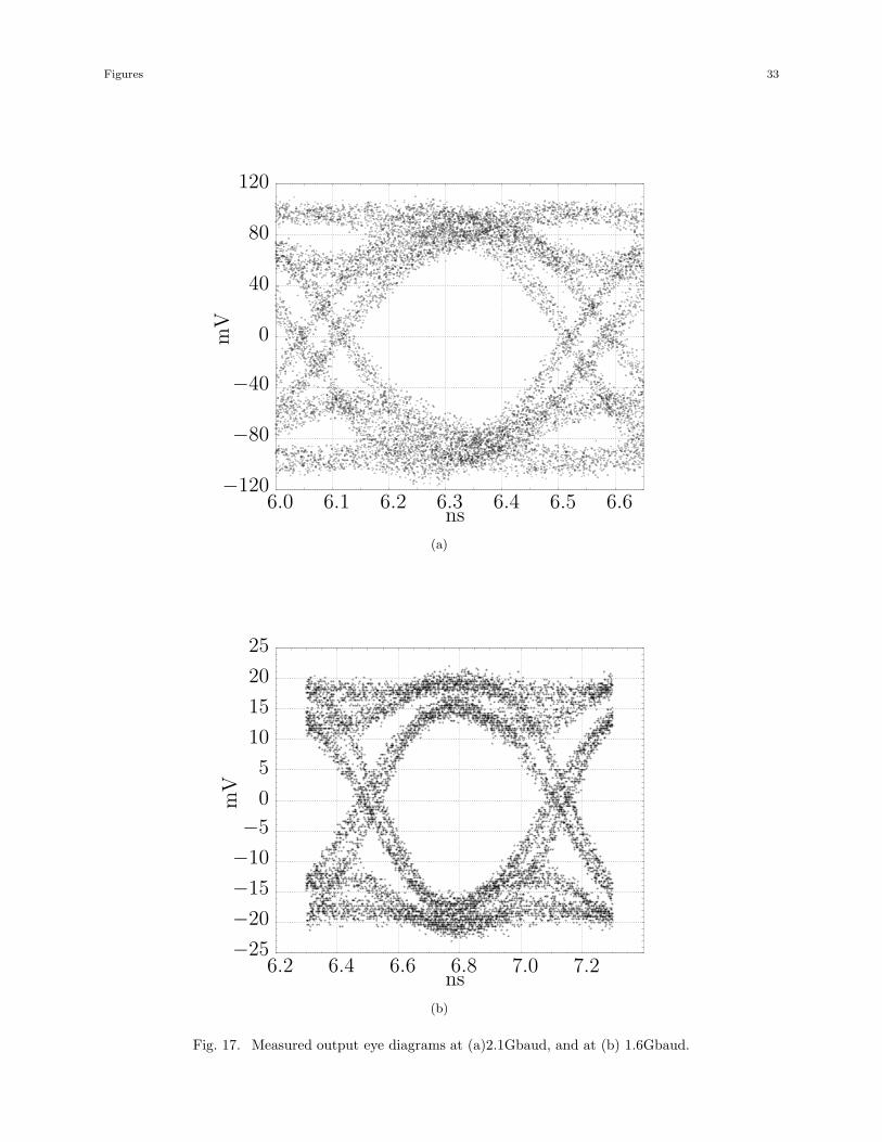
Figure 17(a) and Figure 17(b) display the measured single-sided output eye diagrams for operation at 2.1
and 1.6 Gbaud respectively. An open eye is obtained for single-sided output voltages extending from 4mV
to 500mV. Table IV summarizes the performance of the prototype chip.
[Table 4 about here.]
14
VII. Conclusions
This paper presented an area and power efficient technique for boosting the bandwidth of broadband
systems using optimized on-chip inductors as shunt-peaking elements. Simple, accurate inductance expres-
sions were used in a lumped circuit inductor model to facilitate circuit design. The analytical expressions of
this inductor model permitted inductor circuit problems to be posed as geometric programs so that globally
optimal solutions could be obtained easily, with no iteration needed on the part of the designer.
These bandwidth extension and circuit optimization techniques were applied in the implementation of a
2.125Gbaud, 1.6kΩ differential transimpedance preamplifier with an equivalent input current noise of 0.6µA.
The chip has a die area of 0.6mm2, of which less than 15% is consumed by the two inductors. Designed in
a triple metal, single poly, 0.5µm CMOS process, this chip was intended as a test vehicle to demonstrate
how on-chip bandwidth extension techniques can push the limits of low-cost CMOS processes. To the best
of the authors’ knowledge, this chip is the first CMOS amplifier to use on-chip planar, spiral inductors for
bandwidth enhancement.
VIII. Acknowledgments
The authors would like to thank Rockwell International for fabricating the chips. Particularly, they are
obliged to Dr. Christopher Hull and Dr. Paramjit Singh for invaluable discussions on layout and processing.
They would also like to acknowledge Dr. Allen Lu, Dr. Tad Hofmeister and Prof. Leonid Kazovksy for help
with the optical measurements, and to Dr. C. Patrick Yue for helpful discussions on spiral inductors.
15
References
[1] T. H. Lee, The Design of CMOS Radio-Frequency Integrated Circuits, Cambridge University Press, 1998.
[2] T. Yoon and B. Jalali, “Front-end cmos chipset for fiber-based gigabit ethernet,” in Symposium on VLSI
Circuits, , Digest of Technical Papers, June 1998, pp. 188–191.
[3] C. P. Yue, C. Ryu, J. Lau, T. H. Lee, and S. S. Wong, “A physical model for planar spiral inductors on silicon,”
in Proceedings IEEE IEDM’96, 1996.
[4] J. Crols, P. Kinget, J. Craninckx, and M. Steyeart, “An analytical model of planar inductors on lowly doped
silicon substrates for analog design up to 3GHz,” in Symposium on VLSI Circuits, Digest of Technical Papers,
1996, pp. 28–29.
[5] J. N. Burghartz, K. A. Jenkins, and M. Soyuer, “Multilevel-spiral inductors using VLSI interconnect technology,”
IEEE Electron device letters, vol. 17, no. 9, pp. 428–430, September 1996.
[6] R. B. Merrill, T. W. Lee, H. You, R. Rasmussen, and L. A. Moberly, “Optimization of high Q integrated
inductors for multi-level metal CMOS,” in Proceedings IEEE IEDM’95, 1995, pp. 38.7.1–38.7.4.
[7] K. B. Ashby, I. A. Koullias, W. C. Finley, J. J. Bastek, and S. Moinian, “High Q inductors for wireless
applications in a complementary silicon bipolar process,” IEEE Journal of Solid-State Circuits, vol. 31, no. 1,
pp. 4–9, January 1996.
[8] H. M. Greenhouse, “Design of planar rectangular microelectronic inductors,” IEEE Transactions on parts,
hybrids, and packaging, vol. PHP-10, no. 2, pp. 101–109, June 1974.
[9] E. B. Rosa, “Calculation of the self-inductances of single-layer coils,” Bull. Bureau of Standards, vol. 2, no. 2,
pp. 161–187, 1906.
[10] S. S. Mohan, M. Hershenson, S. P. Boyd, and T. H. Lee, “Simple accurate expressions for planar spiral induc-
tances,” IEEE Journal of Solid-State Circuits, 1999, To appear.
[11] S. S. .Mohan, “Modeling, design, and optimization of on-chip inductors and transformers,” PhD Oral Exami-
nation, Electrical Engineering Department, Stanford University, June 1999, http://smirc.stanford.edu.
[12] J. C. Maxwell, A Treatise on Electricity and Magnetism, Dover, 3 edition, 1967.
[13] R. J. Duffin, E. L. Peterson, and C. Zener, Geometric Programming — Theory and Applications, Wiley, 1967.
[14] Y. Nesterov and A. Nemirovsky, Interior-point polynomial methods in convex programming, vol. 13 of Studies in
Applied Mathematics, SIAM, Philadelphia, PA, 1994.
[15] S. Boyd and L. Vandenberghe, “Introduction to convex optimization with engineering applications,” Course
Notes, 1997, http://www-leland.stanford.edu/class/ee364/.
[16] M. Hershenson, S. P. Boyd, and T. H. Lee, “GPCAD: A tool for CMOS op-amp synthesis,” in Digest of Technical
Papers IEEE International Conference on Computer-Aided Design, 1998, to appear.
[17] S. P. Boyd M. Hershenson, S. S. Mohan and T. H. Lee, “Optimization of inductor circuits via geometric
programming,” in Design Automation Conference, session 54.3, June 1999, pp. 994–998.
[18] R. G. Smith and S. D. Personik, “Receiver design for optical communication systems,” in Topics in Applied
Physics : Semiconductor Devices for Optical Communication, vol. 39, pp. 89–160. Springer-Verlag, Berlin, Ger-
many, second edition, 1982.
[19] Norman Scheinberg, Robert J. Bayruns, and Timothy M. Laverick, “Monolithic GaAs transimpedance amplifiers
for fiber-optic receivers,” IEEE Journal of Solid-State Circuits, vol. 26, no. 12, pp. 1834–1839, Dec. 1991.
[20] S. S. Mohan and T. H. Lee, “A 2.125Gbaud 1.6kω transimpedance preamplifier in 0.5µm CMOS,” in Custom
Integrated Circuits Conference, Digest of Technical Papers, May 1999.

16
[21] Z. Lao et al., “25Gb/s AGC amplifier, 22 GHz transimpedan ce amplifier and 27.7GHz limiting amplifier ics
using AlGaAs/GaAs-hemts,” in ISSCC Digest of Technical Papers, 1997, vol. 40, pp. ??–??
[22] A. A. Abidi, “On the choice of optimum FET size in wide-band transimpedance amplifiers,” Journal of Lightwave
Technology, vol. 6, no. 1, pp. 64–66, Jan. 1988.
[23] Tongtod Vanisri and Chris Toumazou, “Integrated high frequency low-noise current-mode optical tran-
simpedance preamplifiers: Theory and practice,” IEEE Journal of Solid-State Circuits, vol. 30, no. 6, pp.
677–685, June 1995.
[24] C. Toumazou and S. M. Park, “Wideband low noise CMOS transimpedance amplifiers for gigahertz operation,”
Electronics Letters, vol. 32, no. 13, pp. 1194–1196, June 1996.
[25] Derek K. Shaeffer and Thomas H. Lee, “A 1.5V, 1.5GHz CMOS low-noise amplifier,” IEEE Journal of Solid-State
Circuits, vol. 32, no. 5, pp. 745–759, May 1997.
[26] C. Patrick Yue and S. Simon Wong, “On-chip spiral inductors with patterned ground shields for Si-based RF
IC’s,” in 1997 Symposium on VLSI Circuits Digest of Technical Papers, 1997, pp. 85–86.

Figures 17
R
C
Vdd
vout
vin
(a)
R C
vout
gmvin
(b)
L
R
C
Vdd
vout
vin
(c)
L
R
C
vout
gmvin
(d)
Fig. 1. Shunt-peaking a common source amplifier. (a)simple common source amplifier, and its (b) equivalentsmall signal model. (c)common source amplifier with shunt peaking and its (d)equivalent small signalmodel.
Figures 18
No peakingOptimum group delayMaximally flatMaximum bandwidth
0 0.20.4
0.4
0.5
0.6
0.6
0.7
0.8
0.8
0.9
1.0
1.0
1.1
1.2 1.4 1.6 1.8 2.0Normalized frequency
Mag
nitu
de
No peakingOptimum group delayMaximally flatMaximum bandwidth
0
0 0.2 0.4 0.6 0.8 1.0 1.2 1.4 1.6 1.8 2.0
−10
−20
−30
−40
−50
−60
−70
−80
−90
Normalized frequency
Pha
se
Fig. 2. Frequency response of shunt-peaked cases tabulated in table I.
Figures 19
Vdd
Lbondwire
R
vout
vin
Cg
Cbondpad
Cd Cload
Fig. 3. Shunt-peaking with a bond wire inductor
Figures 20
Vdd
L
(R − Rs)
Rs
vout
vin
Cg
CL
Cd Cload
Fig. 4. Shunt-peaking with optimized on-chip inductor
Figures 21
Ls Rs
Cox Cox
CsiCsi RsiRsi
Cs
Fig. 5. Lumped inductor model.
Figures 22
s
w
dout
nI
davg
ρdavgFig. 6. Current sheet approximation of a square spiral
Figures 23
Optical
fiberPhotodiode
Pre-
AGC
Var. gainamp
amp
Decisioncircuit
Clocksynthesizer
Digitaldata
Fig. 7. System overview
Figures 24
Photo
diode
Transimpedance
amplifier
−
+
Cd Cg
Rf
A
Fig. 8. Conventional preamplifier architecture
Figures 25
Common-gate
stage
Photo
diode transimpedance stage
−
+
Cg
Rf
A
Shunt-peaked
Cd
Fig. 9. Preamplifier with shunt peaking
Figures 26
Vdd
L
(R − Rs)
Rs
Rf
vout
iin Cin Cg
CL
Cd Cload
Fig. 10. Shunt-peaked transimpedance stage
Figures 27
Fig. 11. Simplified Circuit Diagram

Figures 28
Fig. 12. Preamplifier die photo
Figures 29
Fig. 13. Inductor test structure
Figures 30
real(ZL) measuredreal(ZL) predictedimag(ZL) measuredimag(ZL) predicted
00 0.5 1.0 1.5 2.0 2.5 3.0
200
400
600
800
1000
Frequency (GHz)
Imped
ance
(Ω)
Fig. 14. Simulated and measured one-port impedance of the spiral inductor used for shunt-peaking: dout =180µm, n = 11.75 turns, w = 3.2µm, s = 2.1µm and t = 2.1µm with L

Figures 31
Tra
nsm
peda
nce
(Ohm
s)
0 0.2 0.4 0.6 0.8 1.0 1.2
1200
1400
1600
1800
800
1000
CPD = 100fF
CPD = 300fF
CPD = 500fF
CPD = 700fF
frequency (GHz)
Fig. 15. Simulated transimpedance vs. frequency
Figures 32
00 0.5 1.0 1.5 2.0
10
20
30
40
γ = 2/3
γ = 4/3
γ = 2
frequency (GHz)
pA/√ H
z
Fig. 16. Input referred current noise density
Figures 33
mV
ns
0
40
120
80
−40
−120
−80
6.0 6.1 6.2 6.3 6.4 6.5 6.6
(a)
mV
ns
0
5
10
15
20
−5
−10
−15
−20
−25
25
6.2 6.4 6.6 6.8 7.0 7.2
(b)
Fig. 17. Measured output eye diagrams at (a)2.1Gbaud, and at (b) 1.6Gbaud.
Tables 34
Factor (m) Normalized ω3dB Response
0 1.00 No shunt peaking
0.32 1.60 Optimum group delay
0.41 1.72 Maximally flat
0.71 1.85 Maximum bandwidthTABLE I
Benchmarks for shunt peaking
Tables 35
Attribute Bond wire Planar Spiral
Inductance 0.5 − 4nH 0.2 − 100nHQ 30 − 60 < 10Parasitics CBondpad Rs, Cox, Csi, Rsi
Fluctuations Large SmallTABLE II
Comparison of on-chip inductor realizations
Tables 36
Layout c1 c2 c3 c4
Square 1.27 2.07 0.18 0.13Hexagonal 1.09 2.23 0.00 0.17Octagonal 1.07 2.29 0.00 0.19
Circle 1.00 2.46 0.00 0.20TABLE III
Coefficients for current sheet expression.

Tables 37
Transimpedance (small-signal) 1600Ω (differential)
800Ω (single-ended)Bandwidth (3dB) 1.2GHz
Max. photodiode capacitance 0.6pFMax. input current 1.0mA
Simulated input noise current 0.6µAMax. output voltage swing 1.0Vpp (differential)
(50Ω load at each output) 0.5Vpp (single-ended)Power consumption 115mW (core)
110mW (50Ω driver)
Die area 0.6mm2
Technology 0.5µm CMOSTABLE IV
Performance summary