Embed Size (px)
Citation preview
International Research Journal of Engineering and Technology (IRJET) e-ISSN: 2395 -0056
Volume: 03 Issue: 03 | Mar-2016 www.irjet.net p-ISSN: 2395-0072
© 2016, IRJET | Impact Factor value: 4.45 | ISO 9001:2008 Certified Journal | Page 40
Structural, Optical and Sensitive Properties of Ag-Doped Tin Oxide Thin Films
Ahmad Z. Al-Janaby 1, Hamid S. Al- Jumaili 1
1Department of physics, College of Education for pure Science, University of Anbar, Al-Anbar, Iraq
[email protected], [email protected]
---------------------------------------------------------------------***---------------------------------------------------------------------Abstract - The present paper a SnO2 (Pure) and Ag doped thin films at different concentration (3, 5 and 7 vol.%) of Ag, were prepared by chemical spray pyrolysis. The films deposited onto glass slides were first cleaned with detergent water and then dipped in acetone and discusses the structural, optical and sensitive properties of Ag-doped tin oxide thin film prepared on glass substrate by the spray pyrolysis technique at a temperature of 400 C. X-ray diffraction study shows that the film was tetragonal rutile structure of SnO2. Morphology analysis studied by atomic force microscopy (AFM) and reveals that the grain size of the prepared thin film is approximately (73.41-111.62) nm, with a surface roughness of (2.18 – 2.79) nm as well as root mean square of (2.69 -3.39) nm for SnO2(pure)and Ag-doping, Optical characteristics were studied by UV/VIS Spectrophotometer at (300- 1100 nm) and observed that the transmission value was more than 75 % at the visible wavelength range. The direct energy gap (Eg) ranged between (2.73-3.22) eV, is measured by UV/VIS., and studied the sensor properties t0 NO2 gas with 3% ratio at a constant voltage of 6V, to found the optimum operation temperature at 150°C for all films, also the sensor work in room temperature. The sensitivity increases with temperature to arrive (81.6%) for SnO2: Ag films at 250°C. The response time was (5.4sec) and the recovery time was (27sec) for SnO2: Ag gas sensor. The results obtained that SnO2 film prepared by chemical spray pyrolysis pure and doped by Ag were a good sensitive for NO2 gas.
Key Words: Structural, Optical and Sensitive Properties, Thin Film, SnO2: Ag.
1.INTRODUCTION The study and application of thin film technology is entirely entered in to almost all the branches of science and technology. Present study which describes the synthesis and study of structural, optical and sensitive characteristics of Ag doped tin oxide (SnO2) is really more interesting for researchers due to its vast applications. Due to the properties like reflectivity, transparency, low electrical sheet resistance etc., tin oxide thin films has immense applications such as gas sensing material for photovoltaic cell in transistors, transparent conductive electrode for solar cells photochemical and photoconductive devices in liquid crystal display [1] gas sensor devices [2,3]. Till to day so many
methods were adopted to synthesize doped or un-doped tin oxide films such as R.F. Magnetron Co- sputtering, Thermal Evaporation, and Chemical Vapor Deposition, Laser Pulse Evaporation, Sol-Gel, Spray Pyrolysis and ultrasonic spray pyrolysis [4, 5, and 6]. Tin oxide crystallizes tetragonal rutile structure [7, 8] with unit cell parameters a=b= 4.737A and c= 3.186 A. It is an n-type semiconductor having high band gap energy (≈ 3.6 eV) [9, 10] with high chemical and mechanical stabilities [11] and is more transparent in the region of visible spectrum due to high band gap, having high electrical conductivity due to free electrons in oxygen vacancy holes [ 12, 13].
2. EXPERIMENTAL A SnO2 (Pure) and Ag doped thin films at different concentration (3, 5 and 7 vol.%) of Ag, were prepared by chemical spray pyrolysis. The films deposited onto glass slides were first cleaned with detergent water and then dipped in acetone. Spray solution was prepared by mixing 0.1 M aqueous solutions of SnO2, and AgNO3 at ratio (3 ,5 and 7 vol.%) using a magnetic stirrer. The automated spray solution was then transferred to the hot substrate kept at the normalized deposition temperature of (400°C) using filtered air as carrier gas at a flow rate normalized to approximately (3) ml/min. To prevent the substrate from excessively cooling, the prepared solution was sprayed on the substrate for 10 s with 15 s intervals. The films had a uniform thickness of range (400) nm. The structural properties were determined by X-ray diffraction (XRD; Shimadzu) with CuKα radiation (λ= 0.15406 nm). Film morphology was analyzed by atomic force microscope (AFM)-type (CSPM). The optical absorption and transmission spectra were obtained using a UV-VIS spectrophotometer 6800JENWAY, Germany) within the wavelength range of (300-1100) nm. For measuring this parameter (sensitivity, response time, …. etc.) We depend upon the difference of resistance or the current through films when the surface of thin films dispose to (NO2) at certain temperature for measuring the sensitivity of films and knowing the temperature through or by thermocouple of heater. we used the system to know the sensitivity for different gases and they are from the following parts .1-Vacuum pumping (Rotary). 2-Connecting pipes. 3- Measurement for vacuum. 4- Chamber cylindrical stainless steel, diameter 30cm and 35cm high, and the chamber contain the following, A- Let for testing gas. B- valve for entering the air after vacuum. C- Glass window. At the
www.spm.co
m.cn
International Research Journal of Engineering and Technology (IRJET) e-ISSN: 2395 -0056
Volume: 03 Issue: 03 | Mar-2016 www.irjet.net p-ISSN: 2395-0072
© 2016, IRJET | Impact Factor value: 4.45 | ISO 9001:2008 Certified Journal | Page 41
bottom or base of the chamber there is an electric heater as well as Thermocouple K-type it is used for controlling the operating temperature and for sensor electrodes. 5-DC-Power supply. 6- Resistance measurement. 7- Laptop for recording the difference of sensor current, when there is percent from gas which enrich the sensor by pipe to the inside of chamber to give the real sensitivity. We can describe the operation of testing the sensor that , we open the testing chamber and put the sensor over the heater and connecting the Al- Electrodes deposed on films with special connecting current and after that closed the chamber firmly and applied (6V) voltage between the sensor electrode , reading the changing in film resistance with time and measuring the current and voltage in the case of there is no gas , then pumping the testing gas and reading the changing in resistance film with times to know the effect of the gas upon the film and from that we can calculate the sensitivity and for the relation;
100
Ra
RRgS a (1)
As well as to know the response time and recovery time and the effect of temperature, doping percent and grain size for thin.
3. RESULTS AND DISCUSSIONS
3.1 Structural and Optical Properties The structure of the prepared tin oxide thin films was investigated by XRD. Figure (1) shows the graph between (2Ө) versus diffracted ray intensity. the major diffraction peaks at 2Ө = (34.4), (26.10), (38.2), and (51.3) for SnO2 (pure) and SnO2: Ag 3,5 and 7 VOL. %, respectively. Thus, the experimental results proved that the polycrystalline nature of the prepared samples as depicted in Figure (1). The result corresponds with that described by Khadair et al [14]. Moreover, an increase in the main peak intensity is observed in the presence of Ag. A comparison with ASTM card 41-1445, reveals that the tin oxide thin film exhibits a crystal structure tetragonal type with a preferred orientation (101) and other planes, i.e., (110), (200), and (211) for 2Ө = (26.10), (38.20), and (51.30). This result agrees with that reported by Sabria et al [15]. The crystalline size (D) is determined from main pack at 2Ө= (34.40) and found to be equal to (34-52) nm. Table (1) passed on Scherer formula [13].
Fig -1: X-ray diffraction patterns of SnO2, SnO2: Ag thin films
Table -1: Average Crystallite size, d (101) and FWHM for Ag doped tin dioxide in comparison with undoped tin dioxide.
FWHM
d(101) (A)
Average Crystallite sizes from XRD (nm)
Doping ratio
0.172 2.66 52 Pure
0.177 2.61 50 (3vol.%)
0.154 2.61 43 (5vol.%)
0.180 2.65 34 (7vol.%)
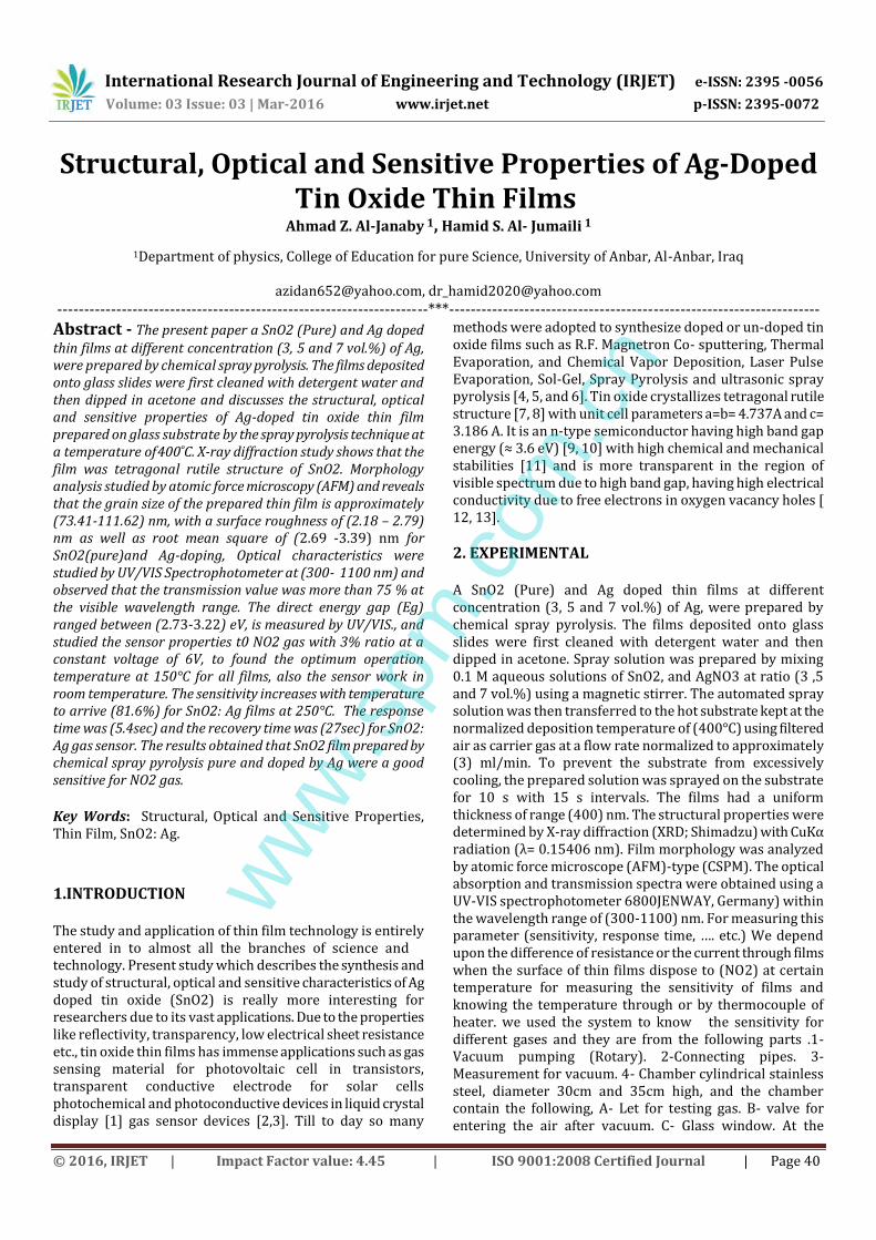
Figure (2) displays AFM image of the films at (pure, 3, 5, and 7 VOL. %) on glass. It shows the presence of homogenous grains throughout the film. The grain size of thin film is (73.41-111.62) nm for the described different concentration. The grain size, Root mean square (RMS) and roughness of these films are shown in table 2. The root main square and roughness (R) are equal to (3.39, 2.82, 2.69 and 2.72) nm, (2.79, 2.3, 2.18 and 2.23) nm respectively. Therefore, the film roughness decreases with decreases of grain size.
Fig -2: The atomic force microscope (a) 2-D and (b) 3-D Image of prepared films Table -2: The Average grain sizes and roughness average for undoped and doped SnO2 films.
Doping ratio Average grain sizes from AFM
(nm)
Root mean square(nm)
Roughness Average (nm)
(Pure) 111.62 3.39 2.79
(3 vol.%) 100.63 2.82 2.3
(5 vol.%) 95.62 2.69 2.18
(7 vol.%) 73.41 2.72 2.23
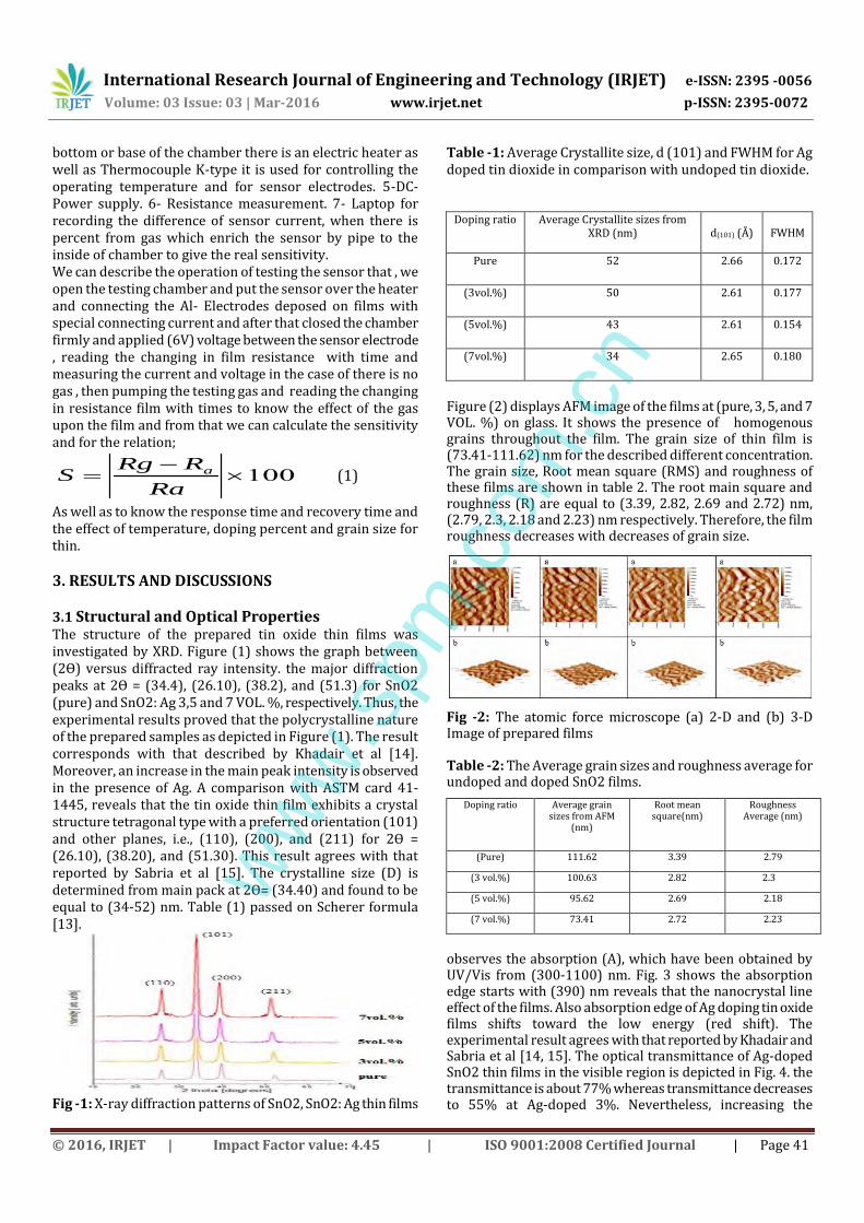
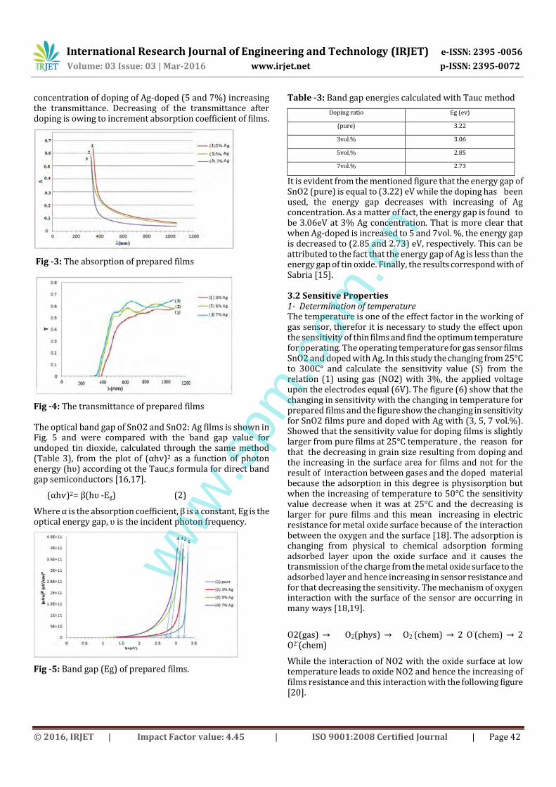
observes the absorption (A), which have been obtained by UV/Vis from (300-1100) nm. Fig. 3 shows the absorption edge starts with (390) nm reveals that the nanocrystal line effect of the films. Also absorption edge of Ag doping tin oxide films shifts toward the low energy (red shift). The experimental result agrees with that reported by Khadair and Sabria et al [14, 15]. The optical transmittance of Ag-doped SnO2 thin films in the visible region is depicted in Fig. 4. the transmittance is about 77% whereas transmittance decreases to 55% at Ag-doped 3%. Nevertheless, increasing the
www.spm.co
m.cn
International Research Journal of Engineering and Technology (IRJET) e-ISSN: 2395 -0056
Volume: 03 Issue: 03 | Mar-2016 www.irjet.net p-ISSN: 2395-0072
© 2016, IRJET | Impact Factor value: 4.45 | ISO 9001:2008 Certified Journal | Page 42
concentration of doping of Ag-doped (5 and 7%) increasing the transmittance. Decreasing of the transmittance after doping is owing to increment absorption coefficient of films.
Fig -3: The absorption of prepared films
Fig -4: The transmittance of prepared films The optical band gap of SnO2 and SnO2: Ag films is shown in Fig. 5 and were compared with the band gap value for undoped tin dioxide, calculated through the same method (Table 3), from the plot of (αhv)2 as a function of photon energy (hʋ) according ot the Tauc,s formula for direct band gap semiconductors [16,17].
(αhѵ)2= β(hʋ -Eg) (2)
Where α is the absorption coefficient, β is a constant, Eg is the optical energy gap, ʋ is the incident photon frequency.
Fig -5: Band gap (Eg) of prepared films.
Table -3: Band gap energies calculated with Tauc method
Doping ratio Eg (ev)
(pure) 3.22
3vol.% 3.06
5vol.% 2.85
7vol.% 2.73
It is evident from the mentioned figure that the energy gap of SnO2 (pure) is equal to (3.22) eV while the doping has been used, the energy gap decreases with increasing of Ag concentration. As a matter of fact, the energy gap is found to be 3.06eV at 3% Ag concentration. That is more clear that when Ag-doped is increased to 5 and 7vol. %, the energy gap is decreased to (2.85 and 2.73) eV, respectively. This can be attributed to the fact that the energy gap of Ag is less than the energy gap of tin oxide. Finally, the results correspond with of Sabria [15]. 3.2 Sensitive Properties 1- Determination of temperature The temperature is one of the effect factor in the working of gas sensor, therefor it is necessary to study the effect upon the sensitivity of thin films and find the optimum temperature for operating. The operating temperature for gas sensor films SnO2 and doped with Ag. In this study the changing from 25°C to 300C° and calculate the sensitivity value (S) from the relation (1) using gas (NO2) with 3%, the applied voltage upon the electrodes equal (6V). The figure (6) show that the changing in sensitivity with the changing in temperature for prepared films and the figure show the changing in sensitivity for SnO2 films pure and doped with Ag with (3, 5, 7 vol.%). Showed that the sensitivity value for doping films is slightly larger from pure films at 25°C temperature , the reason for that the decreasing in grain size resulting from doping and the increasing in the surface area for films and not for the result of interaction between gases and the doped material because the adsorption in this degree is physisorption but when the increasing of temperature to 50°C the sensitivity value decrease when it was at 25°C and the decreasing is larger for pure films and this mean increasing in electric resistance for metal oxide surface because of the interaction between the oxygen and the surface [18]. The adsorption is changing from physical to chemical adsorption forming adsorbed layer upon the oxide surface and it causes the transmission of the charge from the metal oxide surface to the adsorbed layer and hence increasing in sensor resistance and for that decreasing the sensitivity. The mechanism of oxygen interaction with the surface of the sensor are occurring in many ways [18,19].
O2(gas) → O2(phys) → O2¯(chem) → 2 O¯(chem) → 2
O2¯(chem)
While the interaction of NO2 with the oxide surface at low temperature leads to oxide NO2 and hence the increasing of films resistance and this interaction with the following figure [20].
www.spm.co
m.cn
International Research Journal of Engineering and Technology (IRJET) e-ISSN: 2395 -0056
Volume: 03 Issue: 03 | Mar-2016 www.irjet.net p-ISSN: 2395-0072
© 2016, IRJET | Impact Factor value: 4.45 | ISO 9001:2008 Certified Journal | Page 43
NO2+Sn2+ adsorption
2Sn3+ - NO2 desorption
(Sn3+ - O¯ ) + NO2(Sn3+ - O¯) desorption
2Sn3+ + O2
NO2 gas interact with the surface SnO2 on situation Sn and hence the electronics catch leading decreasing in electric connecting the film, this lead to decrease the sensitivity. We can describe this interaction NO2 gas with SnO2 to catch electronics from oxygen adsorbed physically to gain desorption at NO2 gas particles at low temperature according to following equation [21]. NO2(gas) + e¯ → NO2¯ (ads) NO2(ads) + O¯ (ads) → NO (gas) + 2O2
¯ (ads) It was showed at this Fig. 6. When the temperature at 50°C it gains balance between SnO2 oxygen and the atmosphere oxygen to settle the conducting value and the chemical interaction begin chemisorption to NO2 gas with the oxide surface and this lead to translate of electronics to the surface and cause increasing in conducting, then increasing in sensitivity. From the observed the Fig. 6 it showed the sensitivity value for doped films is larger than the pure films it between double to three. The forms of sensitivity showed that the pure and doping films have peak lies between 125-150°C, it is because the mechanism of the interaction gas with the sensor surface. the response of sensor depend upon two factors [22], the first the fast chemical interaction upon the grains surface and the other diffusion velocity the particle of the gas inside the oxide surface , at low temperature the sensor response determine with the fast of chemical interaction , while at high temperature the sensor response determine with the diffusion velocity of gas in sensor surface , while at intermediate temperature the velocity of the two process and these will give the peak at the carved[23].
Fig -6: the changing in sensitivity with the changing in temperature for prepared films. 2- Doping Ratio Effect On Sensitivity
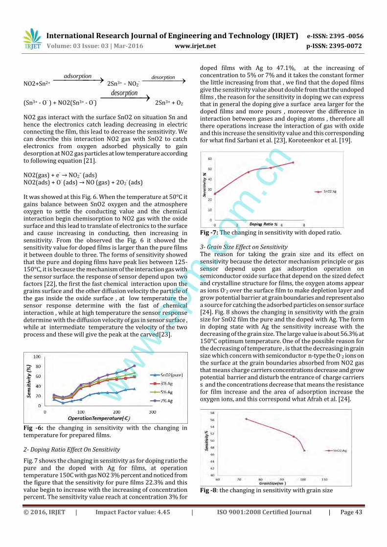
Fig. 7 shows the changing in sensitivity as for doping ratio the pure and the doped with Ag for films, at operation temperature 150C with gas NO2 3% percent and noticed from the figure that the sensitivity for pure films 22.3% and this value begin to increase with the increasing of concentration percent. The sensitivity value reach at concentration 3% for
doped films with Ag to 47.1%, at the increasing of concentration to 5% or 7% and it takes the constant former the little increasing from that , we find that the doped films give the sensitivity value about double from that the undoped films , the reason for the sensitivity in doping we can express that in general the doping give a surface area larger for the doped films and more pours , moreover the difference in interaction between gases and doping atoms , therefore all there operations increase the interaction of gas with oxide and this increase the sensitivity value and this corresponding for what find Sarbani et al. [23], Koroteenkor et al. [19].
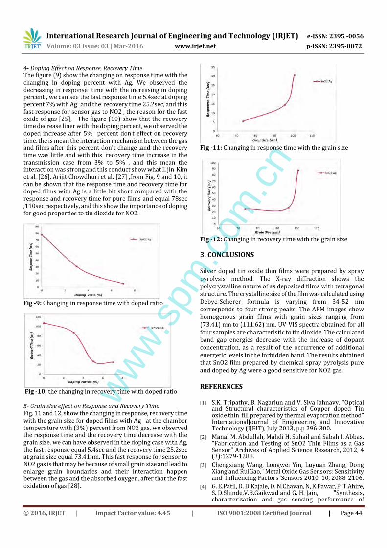
Fig -7: The changing in sensitivity with doped ratio. 3- Grain Size Effect on Sensitivity The reason for taking the grain size and its effect on sensitivity because the detector mechanism principle or gas sensor depend upon gas adsorption operation on semiconductor oxide surface that depend on the sized defect and crystalline structure for films, the oxygen atoms appear as ions O-
2 over the surface film to make depletion layer and grow potential barrier at grain boundaries and represent also a source for catching the adsorbed particles on sensor surface [24]. Fig. 8 shows the changing in sensitivity with the grain size for SnO2 film the pure and the doped with Ag. The form in doping state with Ag the sensitivity increase with the decreasing of the grain size. The large value is about 56.3% at 150°C optimum temperature. One of the possible reason for the decreasing of temperature , is that the decreasing in grain size which concern with semiconductor n-type the O-
2 ions on the surface at the grain boundaries absorbed from NO2 gas that means charge carriers concentrations decrease and grow potential barrier and disturb the entrance of charge carriers s and the concentrations decrease that means the resistance for film increase and the area of adsorption increase the oxygen ions, and this correspond what Afrah et al. [24].
Fig -8: the changing in sensitivity with grain size
www.spm.co
m.cn
International Research Journal of Engineering and Technology (IRJET) e-ISSN: 2395 -0056
Volume: 03 Issue: 03 | Mar-2016 www.irjet.net p-ISSN: 2395-0072
© 2016, IRJET | Impact Factor value: 4.45 | ISO 9001:2008 Certified Journal | Page 44
4- Doping Effect on Response, Recovery Time The figure (9) show the changing on response time with the changing in doping percent with Ag. We observed the decreasing in response time with the increasing in doping percent , we can see the fast response time 5.4sec at doping percent 7% with Ag ,and the recovery time 25.2sec, and this fast response for sensor gas to NO2 , the reason for the fast oxide of gas [25], The figure (10) show that the recovery time decrease liner with the doping percent, we observed the doped increase after 5% percent don't effect on recovery time, the is mean the interaction mechanism between the gas and films after this percent don't change ,and the recovery time was little and with this recovery time increase in the transmission case from 3% to 5% , and this mean the interaction was strong and this conduct show what Il jin Kim et al. [26], Arijit Chowdhuri et al. [27] ,from Fig. 9 and 10, it can be shown that the response time and recovery time for doped films with Ag is a little bit short compared with the response and recovery time for pure films and equal 78sec ,110sec respectively, and this show the importance of doping for good properties to tin dioxide for NO2.
Fig -9: Changing in response time with doped ratio
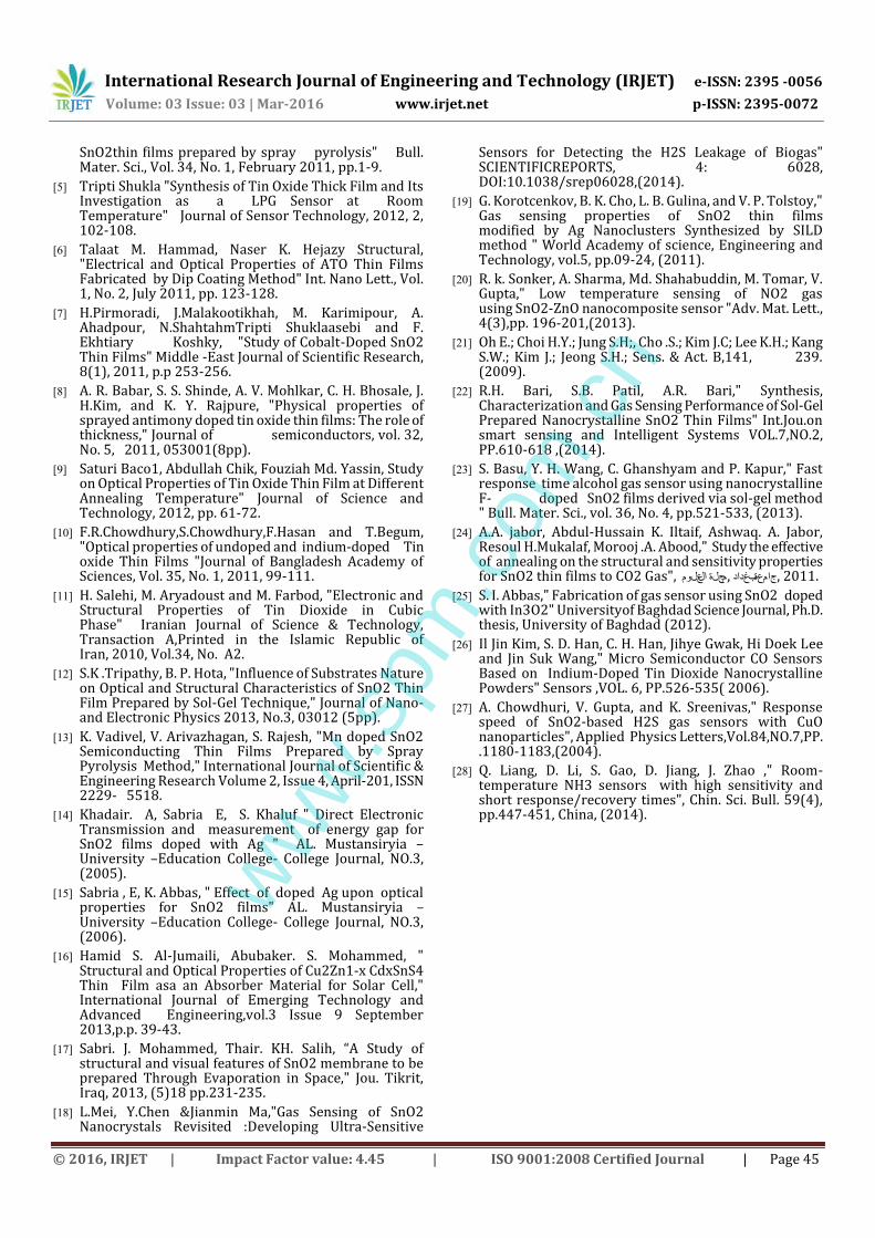
Fig -10: the changing in recovery time with doped ratio 5- Grain size effect on Response and Recovery Time Fig. 11 and 12, show the changing in response, recovery time with the grain size for doped films with Ag at the chamber temperature with (3%) percent from NO2 gas, we observed the response time and the recovery time decrease with the grain size. we can have observed in the doping case with Ag, the fast response equal 5.4sec and the recovery time 25.2sec at grain size equal 73.41nm. This fast response for sensor to NO2 gas is that may be because of small grain size and lead to enlarge grain boundaries and their interaction happen between the gas and the absorbed oxygen, after that the fast oxidation of gas [28].
Fig -11: Changing in response time with the grain size
Fig -12: Changing in recovery time with the grain size 3. CONCLUSIONS Silver doped tin oxide thin films were prepared by spray pyrolysis method. The X-ray diffraction shows the polycrystalline nature of as deposited films with tetragonal structure. The crystalline size of the film was calculated using Debye-Scherer formula is varying from 34-52 nm corresponds to four strong peaks. The AFM images show homogenous grain films with grain sizes ranging from (73.41) nm to (111.62) nm. UV-VIS spectra obtained for all four samples are characteristic to tin dioxide. The calculated band gap energies decrease with the increase of dopant concentration, as a result of the occurrence of additional energetic levels in the forbidden band. The results obtained that SnO2 film prepared by chemical spray pyrolysis pure and doped by Ag were a good sensitive for NO2 gas.
REFERENCES
[1] S.K. Tripathy, B. Nagarjun and V. Siva Jahnavy, "Optical and Structural characteristics of Copper doped Tin oxide thin fill prepared by thermal evaporation method" InternationalJournal of Engineering and Innovative Technology (IJEIT), July 2013, p.p 296-300.
[2] Manal M. Abdullah, Mahdi H. Suhail and Sabah I. Abbas, "Fabrication and Testing of SnO2 Thin Films as a Gas Sensor" Archives of Applied Science Research, 2012, 4 (3):1279-1288.
[3] Chengxiang Wang, Longwei Yin, Luyuan Zhang, Dong Xiang and RuiGao," Metal Oxide Gas Sensors: Sensitivity and Influencing Factors"Sensors 2010, 10, 2088-2106.
[4] G. E.Patil, D. D.Kajale, D. N.Chavan, N, K.Pawar, P. T.Ahire, S. D.Shinde,V.B.Gaikwad and G. H. Jain, "Synthesis, characterization and gas sensing performance of
www.spm.co
m.cn
International Research Journal of Engineering and Technology (IRJET) e-ISSN: 2395 -0056
Volume: 03 Issue: 03 | Mar-2016 www.irjet.net p-ISSN: 2395-0072
© 2016, IRJET | Impact Factor value: 4.45 | ISO 9001:2008 Certified Journal | Page 45
SnO2thin films prepared by spray pyrolysis" Bull. Mater. Sci., Vol. 34, No. 1, February 2011, pp.1-9.
[5] Tripti Shukla "Synthesis of Tin Oxide Thick Film and Its Investigation as a LPG Sensor at Room Temperature" Journal of Sensor Technology, 2012, 2, 102-108.
[6] Talaat M. Hammad, Naser K. Hejazy Structural, "Electrical and Optical Properties of ATO Thin Films Fabricated by Dip Coating Method" Int. Nano Lett., Vol. 1, No. 2, July 2011, pp. 123-128.
[7] H.Pirmoradi, J.Malakootikhah, M. Karimipour, A. Ahadpour, N.ShahtahmTripti Shuklaasebi and F. Ekhtiary Koshky, "Study of Cobalt-Doped SnO2 Thin Films" Middle -East Journal of Scientific Research, 8(1), 2011, p.p 253-256.
[8] A. R. Babar, S. S. Shinde, A. V. Mohlkar, C. H. Bhosale, J. H.Kim, and K. Y. Rajpure, "Physical properties of sprayed antimony doped tin oxide thin films: The role of thickness," Journal of semiconductors, vol. 32, No. 5, 2011, 053001(8pp).
[9] Saturi Baco1, Abdullah Chik, Fouziah Md. Yassin, Study on Optical Properties of Tin Oxide Thin Film at Different Annealing Temperature" Journal of Science and Technology, 2012, pp. 61-72.
[10] F.R.Chowdhury,S.Chowdhury,F.Hasan and T.Begum, "Optical properties of undoped and indium-doped Tin oxide Thin Films "Journal of Bangladesh Academy of Sciences, Vol. 35, No. 1, 2011, 99-111.
[11] H. Salehi, M. Aryadoust and M. Farbod, "Electronic and Structural Properties of Tin Dioxide in Cubic Phase" Iranian Journal of Science & Technology, Transaction A,Printed in the Islamic Republic of Iran, 2010, Vol.34, No. A2.
[12] S.K .Tripathy, B. P. Hota, "Influence of Substrates Nature on Optical and Structural Characteristics of SnO2 Thin Film Prepared by Sol-Gel Technique," Journal of Nano-and Electronic Physics 2013, No.3, 03012 (5pp).
[13] K. Vadivel, V. Arivazhagan, S. Rajesh, "Mn doped SnO2 Semiconducting Thin Films Prepared by Spray Pyrolysis Method," International Journal of Scientific & Engineering Research Volume 2, Issue 4, April-201, ISSN 2229- 5518.
[14] Khadair. A, Sabria E, S. Khaluf " Direct Electronic Transmission and measurement of energy gap for SnO2 films doped with Ag " AL. Mustansiryia –University –Education College- College Journal, NO.3, (2005).
[15] Sabria , E, K. Abbas, " Effect of doped Ag upon optical properties for SnO2 films" AL. Mustansiryia – University –Education College- College Journal, NO.3, (2006).
[16] Hamid S. Al-Jumaili, Abubaker. S. Mohammed, " Structural and Optical Properties of Cu2Zn1-x CdxSnS4 Thin Film asa an Absorber Material for Solar Cell," International Journal of Emerging Technology and Advanced Engineering,vol.3 Issue 9 September 2013,p.p. 39-43.
[17] Sabri. J. Mohammed, Thair. KH. Salih, “A Study of structural and visual features of SnO2 membrane to be prepared Through Evaporation in Space," Jou. Tikrit, Iraq, 2013, (5)18 pp.231-235.
[18] L.Mei, Y.Chen &Jianmin Ma,"Gas Sensing of SnO2 Nanocrystals Revisited :Developing Ultra-Sensitive
Sensors for Detecting the H2S Leakage of Biogas" SCIENTIFICREPORTS, 4: 6028, DOI:10.1038/srep06028,(2014).
[19] G. Korotcenkov, B. K. Cho, L. B. Gulina, and V. P. Tolstoy," Gas sensing properties of SnO2 thin films modified by Ag Nanoclusters Synthesized by SILD method " World Academy of science, Engineering and Technology, vol.5, pp.09-24, (2011).
[20] R. k. Sonker, A. Sharma, Md. Shahabuddin, M. Tomar, V. Gupta," Low temperature sensing of NO2 gas using SnO2-ZnO nanocomposite sensor "Adv. Mat. Lett., 4(3),pp. 196-201,(2013).
[21] Oh E.; Choi H.Y.; Jung S.H;, Cho .S.; Kim J.C; Lee K.H.; Kang S.W.; Kim J.; Jeong S.H.; Sens. & Act. B,141, 239. (2009).
[22] R.H. Bari, S.B. Patil, A.R. Bari," Synthesis, Characterization and Gas Sensing Performance of Sol-Gel Prepared Nanocrystalline SnO2 Thin Films" Int.Jou.on smart sensing and Intelligent Systems VOL.7,NO.2, PP.610-618 ,(2014).
[23] S. Basu, Y. H. Wang, C. Ghanshyam and P. Kapur," Fast response time alcohol gas sensor using nanocrystalline F- doped SnO2 films derived via sol-gel method " Bull. Mater. Sci., vol. 36, No. 4, pp.521-533, (2013).
[24] A.A. jabor, Abdul-Hussain K. Iltaif, Ashwaq. A. Jabor, Resoul H.Mukalaf, Morooj .A. Abood," Study the effective of annealing on the structural and sensitivity properties for SnO2 thin films to CO2 Gas", 2011 ,جامعة بغداد ,مجلة العلوم.
[25] S. I. Abbas," Fabrication of gas sensor using SnO2 doped with In3O2" Universityof Baghdad Science Journal, Ph.D. thesis, University of Baghdad (2012).
[26] Il Jin Kim, S. D. Han, C. H. Han, Jihye Gwak, Hi Doek Lee and Jin Suk Wang," Micro Semiconductor CO Sensors Based on Indium-Doped Tin Dioxide Nanocrystalline Powders" Sensors ,VOL. 6, PP.526-535( 2006).
[27] A. Chowdhuri, V. Gupta, and K. Sreenivas," Response speed of SnO2-based H2S gas sensors with CuO nanoparticles", Applied Physics Letters,Vol.84,NO.7,PP. .1180-1183,(2004).
[28] Q. Liang, D. Li, S. Gao, D. Jiang, J. Zhao ," Room-temperature NH3 sensors with high sensitivity and short response/recovery times", Chin. Sci. Bull. 59(4), pp.447-451, China, (2014).
www.spm.co
m.cn