Embed Size (px)
Citation preview

1
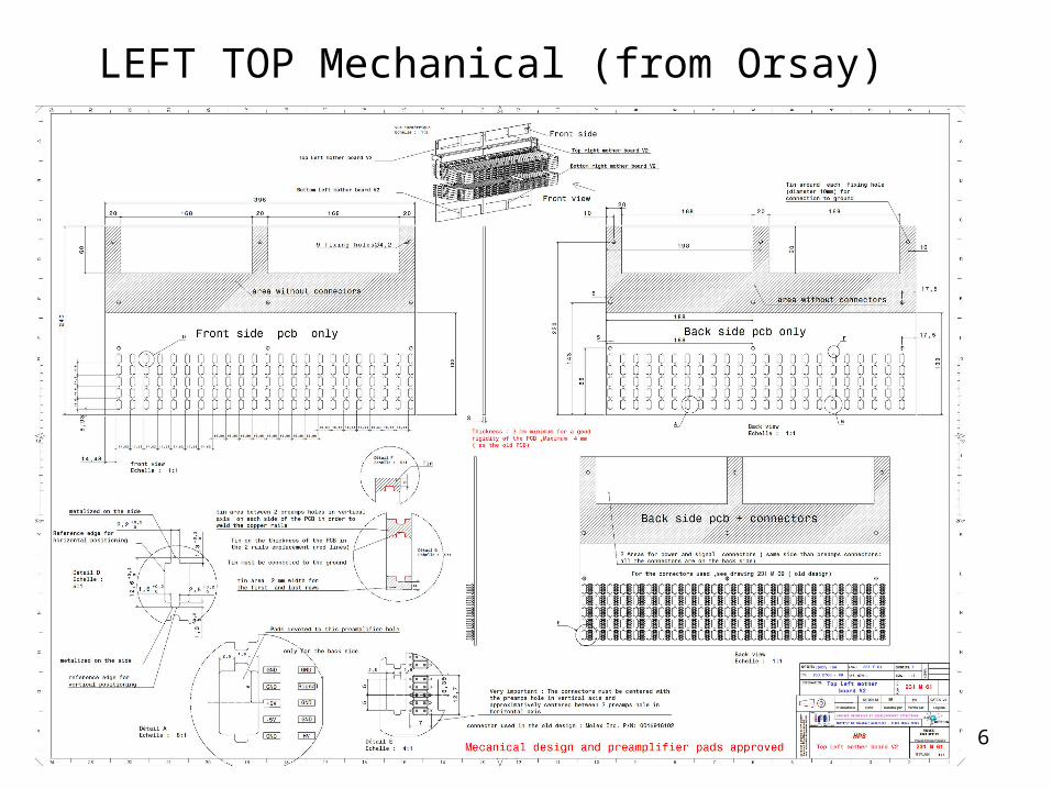
• 4 PCB: LEFT TOP 115 channels, LEFT BOTTOM (115), RIGHT TOP (106), RIGHT BOTTOM (106).
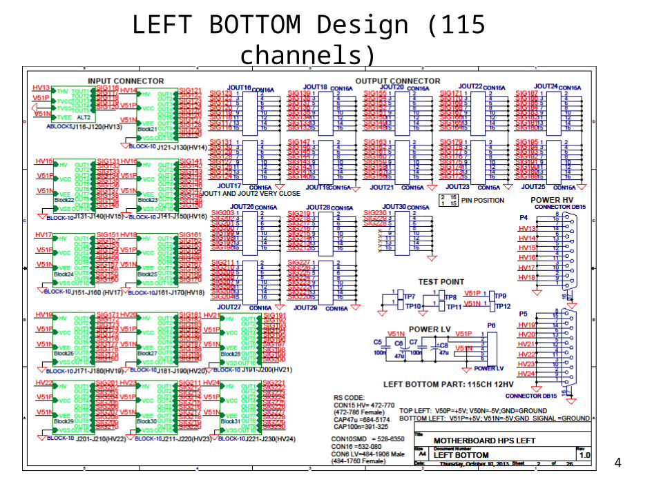
•For LEFT TOP board 115 channels we have:• 115 smd connectors (AMP 10 pin) for preamp very similar to
previous version (pin slightly smaller). It is the same of FT-Cal motherboard.
• 15 TE signal connectors from 16 pin each, equal to previous version.
• 2 HV connectors (15 pin) DSUB 750V, 5A, trough hole different to previous for a easier routing.
• 1 LV connectors (6 pin).
•We can use a very similar HV grouping. •We can use the same cable as discussed with Stepan Stepanyan.
HPS Motherboard Electronic Design

2
Design Block of 10

3
LEFT TOP Design (115 channels)
4
LEFT BOTTOM Design (115 channels)

5
HV Grouping (Proposal)
Jx is the x smd 10 pin connector HVx is the x High Voltage netNEW TOP LEFT (the same as previus project)
BACK SIDE VIEW 115 input connectors 12 HV nets HV1 to HV12
J1 HV1 J6 HV2 J11 HV2 J16 HV3 J21 HV3 J26 HV4 J31 HV4 J36 HV5 J41 HV5 J46 HV6 J51 HV6 J56 HV7 J61 HV7 J66 HV8 J71 HV8 J76 HV9 J81 HV9 J86 HV10 J91 HV10 J96 HV11 J101 HV11J106 HV12J111 HV12J2 HV1 J7 HV2 J12 HV2 J17 HV3 J22 HV3 J27 HV4 J32 HV4 J37 HV5 J42 HV5 J47 HV6 J52 HV6 J57 HV7 J62 HV7 J67 HV8 J72 HV8 J77 HV9 J82 HV9 J87 HV10 J92 HV10 J97 HV11 J102 HV11J107 HV12J112 HV12J3 HV1 J8 HV2 J13 HV2 J18 HV3 J23 HV3 J28 HV4 J33 HV4 J38 HV5 J43 HV5 J48 HV6 J53 HV6 J58 HV7 J63 HV7 J68 HV8 J73 HV8 J78 HV9 J83 HV9 J88 HV10 J93 HV10 J98 HV11 J103 HV11J108 HV12J113 HV12J4 HV1 J9 HV2 J14 HV2 J19 HV3 J24 HV3 J29 HV4 J34 HV4 J39 HV5 J44 HV5 J49 HV6 J54 HV6 J59 HV7 J64 HV7 J69 HV8 J74 HV8 J79 HV9 J84 HV9 J89 HV10 J94 HV10 J99 HV11 J104 HV11J109 HV12J114 HV12J5 HV1 J10 HV2 J15 HV2 J20 HV3 J25 HV3 J30 HV4 J35 HV4 J40 HV5 J45 HV5 J50 HV6 J55 HV6 J60 HV7 J65 HV7 J70 HV8 J75 HV8 J80 HV9 J85 HV9 J90 HV10 J95 HV10 J100 HV11J105 HV11J110 HV12J115 HV12
NEW TOP RIGHT (a little bit different max 2lines for column instead 4)6 groups of 10, 2 group of 9, 1 group of 11, 1 group of 8, 1 group of 6 and 1 group of 3
BACK SIDE VIEW 106 input connectors 12 HV nets HV25 to HV36
J1 HV25 J6 HV25 J11 HV26 J16 HV26 J21 HV27 J26 HV27 J31 HV28 J36 HV28 J41 HV29 J46 HV29 J51 HV30 J56 HV30 J61 HV31 J66 HV31 J70 HV32 J74 HV32 J78 HV33 J82 HV33 J86 HV33 J90 HV35 J94 HV36 J98 HV36 J102 HV36J2 HV25 J7 HV25 J12 HV26 J17 HV26 J22 HV27 J27 HV27 J32 HV28 J37 HV28 J42 HV29 J47 HV29 J52 HV30 J57 HV30 J62 HV31 J67 HV31 J71 HV32 J75 HV32 J79 HV33 J83 HV33 J87 HV34 J91 HV35 J95 HV36 J99 HV36 J103 HV36J3 HV25 J8 HV25 J13 HV26 J18 HV26 J23 HV27 J28 HV27 J33 HV28 J38 HV28 J43 HV29 J48 HV29 J53 HV30 J58 HV30 J63 HV31 J68 HV31 J72 HV32 J76 HV32 J80 HV33 J84 HV33 J88 HV34 J92 HV35 J96 HV35 J100 HV36J104 HV36J4 HV25 J9 HV25 J14 HV26 J19 HV26 J24 HV27 J29 HV27 J34 HV28 J39 HV28 J44 HV29 J49 HV29 J54 HV30 J59 HV30 J64 HV31 J69 HV31 J73 HV32 J77 HV32 J81 HV33 J85 HV33 J89 HV34 J93 HV35 J97 HV35 J101 HV36J105 HV36J5 HV25 J10 HV25 J15 HV26 J20 HV26 J25 HV27 J30 HV27 J35 HV28 J40 HV28 J45 HV29 J50 HV29 J55 HV30 J60 HV30 J65 HV31 J106 HV36
6
LEFT TOP Mechanical (from Orsay)

7
• 4 PCB: LEFT TOP 115 channels, LEFT BOTTOM (115), RIGHT TOP (106), RIGHT BOTTOM (106).
• Board Dimension is 400x240 mm and 143 component each.• Board Thickness = 2.5 mm.
• Layout specifications:• 10 Layers (3 signals + 1 for High Voltage + 1 fan-out + 5 GND).• 115 signal traces with 50 Ohms impedance.• Signal: 0.2 mm line width and 0.2 mm min. spacing.• HV: 0.5 mm line width and 0.8 mm min. spacing.• Ground ring between two signals.
HPS Motherboard Layout Design

8
LEFT TOP Routing (preliminary)

9
Routing Zoom on 3 columns

10
• Mechanical Specifications with Orsay. Done!• Design of LEFT TOP and LEFT BOTTOM boards. Done!• Layout routing of LEFT TOP and LEFT BOTTOM boards. NOW
• Design of RIGHT TOP and RIGHT BOTTOM boards with the correct HV grouping. November.
• Layout routing of RIGHT TOP and RIGHT BOTTOM boards.
End of year. • Board Productions and Assembly (with the same company used for
the FT-Cal). rough estimate 5Keuro. January 2014. • Test on Electrical connections and Full crosstalk test with FT-Cal
crystals. February 2014.
HPS Motherboard Next Steps