Embed Size (px)
Citation preview

ANAND INSTITUTE OF HIGHER TECHNOLOGYKAZHIPATTUR
Department of Electronics & Instrumentation EngineeringName: Mrs.K.Mohana/Ms.V.Vishalakshi Year/Sem : II / IVSub/ Code : Digital Logic Circuits
PART A
UNIT I-NUMBER SYSTEMS & BOOLEAN ALGEBRA
1. Convert the hexadecimal number E3FA to binary. (EI Nov 2007)
Solution:E3FA16 – Hexadecimal E 3 F A11102 00112 11112 10102
So the equivalent binary value is 11100011111110102
2. Perform the following conversion (1029)10 to gray (EE May 2006)
Solution:1 0 2 9 ----- Decimal0001 0000 0010 1001 ----- BCD0001 0000 0011 1101 ----- Gray
Thus the Gray code of 102910 is 00010000001111012
3. Add 1A816 and 67B16 (EE Nov 2004)
Solution:1 A 816
6 7 B16
--------------------------8 2 316
--------------------------= 82316
4. Show the Karnaugh map with the encircled groups for the Boolean function,F =C’ +A’D’ + A’B’D’ . (EE May 2006)
Solution:
1 1 11 1 11 1
1 1 1
1

5. Perform 2s complement subtraction of 010110-100101. (Nov 2004)
Solution:1’s complement of minuend100101 = 0110102’s complement of 011010 = 011011Addition of 010110 + 011011 = 110001There is no end carry.Therefore, the answer is –(2’s complement of 110001)
Answer = - 001111
6. Apply Demorgan’s theorems to simplify (A+BC') '. (Apr 2004)
Solution:(A +BC') ' = A'. (BC') '= A' . (B'+ C)
7. Plot the expression on K-Map F (w, x, y) =Σ (0,1,3,5,6) + d(2,4). (Apr 2004)
Solution:
W XY1 1 1 XX 1 1
F = x' +x y' + w’
8. If A and B are Boolean variables and if A=1 and (A+B) ' = 0, find B. (Nov 2003)
Solution:If B=0 (A+B)’=0
If B=1 (A+B)’=0 Hence the value of B= 0 (or) 1 i.e Don’t care
12. If A and B are Boolean variables check if (A.A') (A A')=(B+B') (B' B). (Apr 2003)
A A’ AA’ AA’
(AA’) (AA’) B B’ B+B’ B’B (B+B’) (B’B)
0 1 0 1 1 0 1 1 1 01 0 0 1 1 1 0 1 1 0
L.H.S #R.H.S (Not equal)
14. What is the feature of gray code? What are its applications (EC Nov 2007/May 2006)
Solution:
The advantage of gray code also called reflected code over pure binary numbers is that a number in gray code changes by only one bit as it proceeds from one number to the next. A typical application of the reflected code occurs when the analog data are represented
2

by a continuous change of a shaft position. The shaft is portioned into segments and each segment is assigned a number. If adjacent segment are made to correspond to adjacent reflected-code numbers, ambiguity is reduced when detection is sensed in the line that separates any two segments.
So in 3-bit code, error may occur due to one bit position, other two bit positions of adjacent sectors are always same and hence there is no possibility of error. Thus in 3-bit code, probability of error is reduced to 66 % and in 4-bit code it is reduced upto 25%.
15. Convert the gray code number 11011 to binary. (Nov 2006)
Solution:
gray code
binary code =10010
16. What is even parity? (Nov 2006)
Solution:
A parity bit is an extra bit included with a message to make the total number of 1’s either odd or even. If the total number of 1’s is even then it is called even parity.
17. Find the 2’s complement and 1’s complement of 101101. (EC May 2006)
Solution:
1’s complement of 101101 = 010010 2’s complement of 101101 = 010010 1 ---------- 010011
----------18. Simplify X1 +X1 X2. (EC May 2006)
Solution:x1 + x1x2 = x1(1+x2)
= x1
19. Find the standard sum for the following function. (EC May 2006)f = x1 x2 x3 + x1 x3 x4 + x1 x2 x4.
Solution:f = x1 x2 x3 + x1 x3 x4 + x1 x2 x4 = x1 x2 x3(x4+x4’) + x1(x2+x2’) x3x4+x1x2(x3+x3’) x4 = x1x2x3x4 +x1x2x3x4’+x1x2’x3x4 + x1x2x3’x4
3

(Hint: standard sum means canonical POS)
20. Convert binary number 11011110 into its decimal equivalent. (May 2007)
Solution: 1 1 0 1 1 1 1 0 ----------- 0 * 20 =0 ----------- 1 * 21=2 ----------- 1 * 22=4 ----------- 1 * 23=8 ----------- 1 * 24=16 ----------- 0 * 25=0 ----------- 1 * 26=64 ----------- 1 * 27=128 ------- 222
21. Mention any two applications of Demorgan’s theorem. (May 2007)
Solution: - Simplification of Boolean expression
- To convert AND to OR and vice versa
22. Simply the following Boolean function: (May 2007) (a) x(x’+y) (b) xy + x’z +yz
Solution: (a) xx’ + xy (xx’ =0) = xy
(b) xy + x’z + yz (by consensus theorem)
= xy + x’z 23. Convert the binary number 1011 to gray code. (May 2007)
Solution: Gray code of 1011 is 1110
24. Minimise the function using Boolean algebra f = x(y+w’z)+wxz. (May 2007)
Solution: F = x(y+w’z) + wxz = xy + xw’z + wxz = xy +xz(w’ + w) = xy +xz
4

25. Determine the decimal number represented by 101101.10101. (May 2008)
Solution:
101101.10101 --------- 1*2-5 =0.03125
---------- 0*2-4 = 0 ----------- 1*2-3 = 0.125
------------0* 2-2 =0 -------------1* 2-1 =0.5 ---------------1 *2 0 =1 ----------------0*21 =0 -----------------1*22 =4 -------------------1*23 =8 --------------------0*24 =0 ---------------------1*25 =32 ----------------- 45.65625 ----------------
26. Convert (0.513)10 to octal. (Nov 2007)
Solution: 0.513 * 8 = 4.104 4 0.104 * 8 = 0.832 0 0.832 *8 = 6.565 6 0.656 *8 = 5.248 5 0.248 *8 =1.984 1
0.984 *8 = 7.872 7 (0.513)10 =( 0.406517..)8
27. Express F= A+B’C as sum of minterms. (Nov 2007)
Solution:F= A+B’CThe function has three variables A, B, C . The first term A is missing two variables B and C.The second term is missing one variable so F= A (B+B’) (C+C’) + (A+A’) B’C = ABC+ABC’+AB’C’+AB’C+A’B’C+AB’C = ABC+ABC’+AB’C’+AB’C+A’B’C since (x+x = x) = m7 +m6+m4 + m5+m1 (arrange in ascending order)= m1+m4+m5+m6+m7
5

28. Using 2’s complement perform the given subtraction (1001101)2 – (110100)2
Solution: Take 2’s complement for 0110100 --1001011 (Nov 2007)
+ 1--------------
1001100 ------------- 1001101 +1001100 ------------ 10011001 discard the end carry ans is 001100
29. Prove that A+A'B = A + B, Using Boolean algebra. (Nov 2005)
Solution:A+A’B = (A+A') (A+B)
= 1 (A+B) where A+A' = 1= A+B
30. Construct the truth table of F=(AB)(CD).
Solution: S.No A B C D AB CD F=(AB)(CD)
1 0 0 0 0 0 0 02 0 0 0 1 0 1 13 0 0 1 0 0 1 14 0 0 1 1 0 0 05 0 1 0 0 1 0 16 0 1 0 1 1 1 07 0 1 1 0 1 1 08 0 1 1 1 1 0 19 1 0 0 0 1 0 110 1 0 0 1 1 1 011 1 0 1 0 1 1 012 1 0 1 1 1 0 113 1 1 0 0 0 0 014 1 1 0 1 0 1 115 1 1 1 0 0 1 116 1 1 1 1 0 0 0
31. Write the De-morgans theorem. (EI Nov 2007, Nov 2006, Apr 2005, EI May’10)
Solution:
(A+B) ' = A' .B'
(A.B) ' = A' + B'
6

Demorgans laws are mostly useful in simplifying expressions in which products or sum variables are inverted.
32. Simplify XY’+ZXY’ (EI April 2011)
=XY’(1+Z) =XY’
33. Convert (108.2)10 and (108.2)2 into hexadecimal numbers. (EI April 2011)34. What are cyclic codes? (EI May /June 2013)
Cyclic codes are a special type of linear block code that are popularbecause they are very effective for error detection and correction and theircoders and decoders are easy to implement in hardware
35. Simplify the function Y= Σ (1,3,5,7)W XY (EI May /June 2013)
XY
Y=Y
36.What is hamming code? (EI DEC 2013)One of the most common method of error correcting .It consist of k parity bits that are added to n-bit data word forming a new n+k bits 37.What are redundant prime implicants? (EI DEC 2013)
The prime implicant whose each one 1 is covered by atleast one essential prime implicants is called redundant prime implicants.
UNIT II-COMBINATIONAL CIRCUITS
1. Write the procedural steps for the design of combinational circuits. (EI May 2009).
7
1 11 1

Solution:
The design of combinational circuit starts from a specification of the problem culminates in a logic diagram or set of Boolean equations from which the logic diagram can be obtained.
The procedure involves the following steps:
1. From the specifications of the circuit, determine the required number of inputs and outputs, and assign a letter symbol to each.
2. Derive the truth table that defines the required relation ship between inputs and outputs.
3. Obtain the simplified Boolean functions of each output as function of the input variables.
4. Draw the logic diagram.
5. Verify the correctness of the design.
2. Give the truth table for 4 bit priority encoder. (EI May 2009)(Reg 2007)
Solution:
A 4-bit priority encoder (also sometimes called a priority decoder). This circuit basically converts the 4-bit input into a binary representation. If the input n is active, all lower inputs (n-1…0) are ignored:
X3 X2 X1 X0 Y1 Y01 X X X 1 10 1 X X 1 00 0 1 X 0 00 0 0 X 0 0
The circuit operation is simple. Each output is driven by an OR-gate which is connected to the NAND-INV outputs of the corresponding input lines. The NAND gate of each stages receives its input bit, as well as the NAND gate outputs of all higher priority stages. This structure implies that an active input on stage n effectively disables all lower stages n-1.. 0.
Note that the circuit function as specified here does not depend at all on the least significant input bit.
A common use of priority encoders is for interrupt controllers, to select the most critical out of multiple interrupt requests. Due to electrical reasons (open collector outputs), priority encoders with active-low inputs are also often used in practice.
3. Draw the Truth Table of Full Adder. (EI Nov 2007)
8

Solution:
Input Output
C B A Sum Carry
0 0 0 0 0
0 0 1 1 0
0 1 0 1 0
0 1 1 0 1
1 0 0 1 0
1 0 1 0 1
1 1 0 0 1
1 1 1 1 1
Truth Table
4. Realize f= A'B + AB' using minimum universal gates. (Nov 2005)
Solution: f= A'B + AB' = A’
5. Draw a tristate inverter and draw its truth table (Nov 2005).
Solution:
A tri-state buffer is a useful device that allows us to control when current passes through the device, and when it doesn't. Here are two diagrams of the tri-state buffer.
9
A
B
B’

Here's a truth table describing the behavior of an active-high tri-state buffer.
C X Z0 0 Z0 1 Z1 0 01 1 1
6. Draw a combinational logic circuit which can compare whether two bit binary numbers are same or not.
Solution:
(Nov 2005)
Which is similar to EX-NOR operation Y= A’B’+AB
7. What is combinational circuit? Give an example. (Apr 2005)
Solution:A combinational circuit consists of logic gates whose outputs at any time are
determined from the present combination of inputs. Examples of combinational circuits are adder, coder, magnitude comparator etc.
8. What are the universal gates? (Nov 2004)
Solution:NAND and NOR are universal gates, because they replace all the other gates in a
circuit.
9. Obtain 3 level NOR – NOR implementation of f(a,b,c,d,e,f)=[ab+cd ]ef. (Nov 2004) f (a, b, c, d, e, f)=[ab+cd ]ef
Solution:
10
A B Y0 0 10 1 01 0 01 1 1

= abef +cdefF’= (abef + cdef)’
=(abef)’.(cdef)’= a+b+e+f . c+d+e+f
10. Draw a 1 to 2-demultiplexer circuit. (Nov 2003)
Solution:
11. Draw a 2 to 1 multiplexer circuit. (Nov 2003)
Solution:
12. What is demux? (EC Nov 2007/Apr 2004)
11

Solution:Demultiplexer is a circuit that receives information on a single line and transmits this
information on one of 2n possible output lines. A demultiplexer is a decoder with an enable input.
13. Draw a parity checker circuit for 3 bit binary word x1 x2 x3. (May 2006)
Solution:
14. What does LS in 74LS00 indicate? (Nov 2006)
Solution:Low power schottky TTL
15. Define priority encoder. (Nov 2006)
Solution:Encoders establish an input priority to ensure that only the highest-priority input line
is encoded. If priority is given to an input with higher subscript number over one with lower subscript number, then if both D2 and D5 are logic-1 simultaneously, the output will be 101 because D5 has a higher priority over D2.
InputsD0 D1 D2 D3 D4 D5 D6 D7
OutputsX y z
1 0 0 0 0 0 0 0 X 1 0 0 0 0 0 0 X X 1 0 0 0 0 0 X X X 1 0 0 0 0 X X X X 1 0 0 0 X X X X X 1 0 0 X X X X X X 1 0 X X X X X X X 1
0 0 0 0 0 1 0 1 0 0 1 1 1 0 0 1 0 1 1 1 0 1 1 1
16. Realize S(X, Y, Z) =∑ (1,2,3,4) using an appropriate decoder and an external logic gates. (Nov 2006)
12

0 V
A Y0B Y1C Y2 Y3 3:8 Y4 Y5 Y6 Y7EN’
Half adderA
B
C
S
Solution:
= 14 mW 17. Represent a half adder in block diagram form and also its logic implementation. (EC May2006\May2007)
Solution:
Inputs Y = A+ B
A B carry Sum
0 0 0 0
0 1 0 1
1 0 0 1
1 1 1 0
Carry B A
Carry = ABSum B A
Sum =A’B+AB’
18. What are the major categories of logic circuits? (May 2007)
Solution:
13
1
11

A
B
Y
The major categories of logic circuits are combinational logic circuit and sequential logic circuit.
19. Design a 2 input NAND gate using 2: 1 multiplexer. (May 2007)
Solution:
A B Y0011
0101
1000
Io I1
A’ 1
A 2 3
A’ 0
A’B
20. Find the relation between the I/Ps and O/P, shown in figure. Name the operation performed. (May 2008)
Solution:
Y = A’.B’ =( A+B)’
This gate performs the NOR operation.
21. Write the truth table of a 4:1 multiplexer. (May 2008)
Solution:S0 S1 Output
00 I0
14
0
I0 2X1I1 S0
0 V

011011
I1
I2
I3
22. Draw the logic diagram for X=AB +B’C.(Nov 2007)
Solution:
A
B’ C
23. Implement F = (AB’ + A’B)(C+D’) with only NOR gate.(Nov 2007) F = (AB’ + A’B)(C+D’)
Solution:F = AB’C +A’BC +AB’D’+A’BD’F’ = (AB’C +A’BC +AB’D’+A’BD’)’ = (AB’C)’(A’BC)’(AB’D’)’(A’BD’)’F ‘ = (A’+B+C’)(A+B’+C’)(A’+B+D)(A+B’+D)
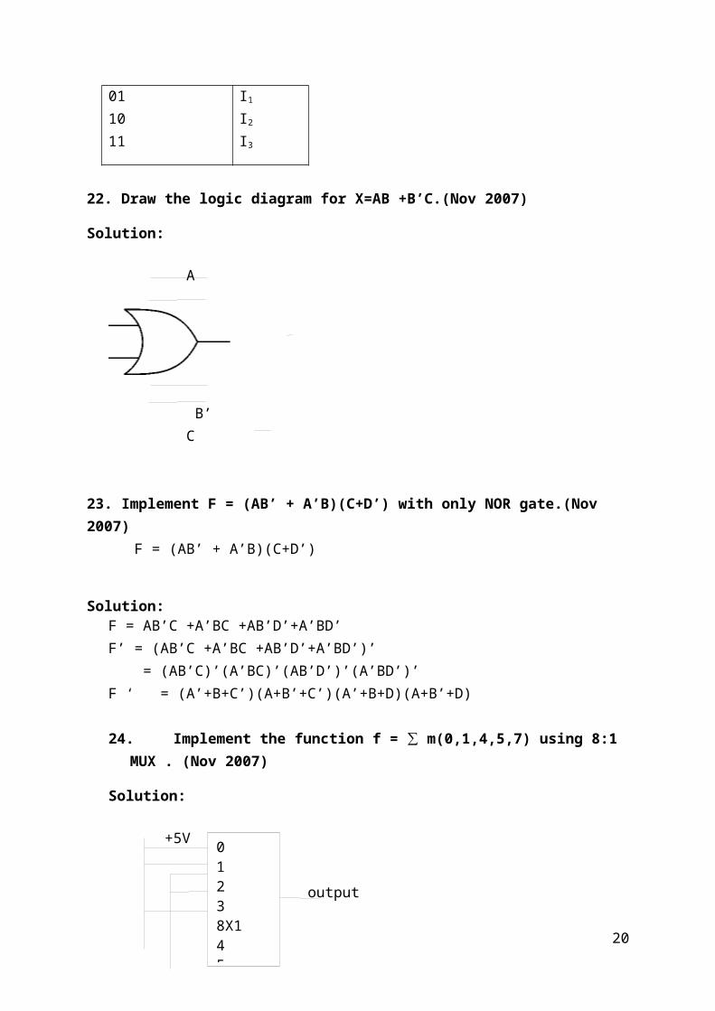
24. Implement the function f = ∑ m(0,1,4,5,7) using 8:1 MUX . (Nov 2007)
Solution:
+5V
output
0V
S0S1S2
25. Specify the use of Multiplexers (EI Nov 2007)
Solution:
15
0123 8X14567

The applications of Multiplexers are1. Data Selection2. Data Routing3. operation Sequencing4. Parallel to serial conversion5. Waveform Generation6. Logic function generation
26. Design a Half Subtractor. (EI April’10)
Solution:X Y D B
0 0 0 0
0 1 1 1
1 0 1 0
1 1 0 0
D= XY’+X’Y=X xor YB=X’Y
27. Implement the following function using only NAND gates F =(x + y)z (EI April’10)
28Write the truth table for half adder? (EI May/June’13)
16
Inputs Y = A+ B
A B carry Sum
0 0 0 0
0 1 0 1
1 0 0 1
1 1 1 0

29Implement y=BC’+AB’+AD using NAND gates? (EI May/June’13) 30.Implement the function F=A.B using nor gate? (EI Nov/Dec’13)
31.How the decoder is used as demultiplexer? (EI Nov/Dec’13) The selection lines of the DEMUX can be used as input lines of decoder and if the data input of the demultiplexer is used as the enable input of the decoder then we can use the
demultiplexer as a decoder.
UNIT III- SYNCHRONOUS SEQUENTIAL CIRCUITS
1. What are shift register counters? List two widely used shift register counters. (EE Dec 2004).
Solution:If the output of a shift register is fed back to the input. a ring counter results. The data
pattern contained within the shift register will recirculate as long as clock pulses are applied.
2. Why is FlipFlop also known as Latch? (EC Nov 2007)Solution:
The difference between a latch and a flip-flop is that a latch does not have a clock signal, whereas a flip-flop always does. Latch is a level sensitive device while flip-flop is an edge sensitive device. Latch is sensitive to glitches on enable pin, whereas flip-flop is immune to that.
3. Compare Moore and Mealy Machine. (EC Nov 2007)
Sl.No
Moore Model Mealy Model
1. Its output is a function of present state only.
Its output is a function of present state as well as present input
2. Input changes does not affect the output
Input changes may affect the output of the circuit
3. It requires more number of states for implementing the function
It requires less number of states for implementing the function
4. Obtain the excitation table of D-FlipFlop (EE May 2006) Q Q(t+1) D
17

0 0 1 1
0 1 0 1
0 1 0
1
5. What are state diagram and state tables? (EE May 2006)
Solution:The time sequence of inputs, outputs and flip-flop states may be enumerated in a state
table and the information available in a state table may be represented graphically called a state diagram. For the design of sequential counters we have to relate present states and next states. The table, which represents the relationship between present states and next states, is called state table. 6. Give the excitation table for JK FlipFlop (EI Nov 2007)
Solution:
Q Q(t+1) J K 0
0
1
1
0
1
0
1
0
1
X
X
X
X
1
0
7. Draw the logic diagram for T FlipFlop (EI Nov 2007)
Solution:
8. How many flip-flops are required to design a mod-7 up-down counter?(Nov2005)
Solution:
18

Qn T
Qn T
Flip Flops required are 2n >= N where N=7 2n >= 7 n = Number of Flip Flops. n = 3 Hence 3 Flip Flops are required
9. What is a sequential circuit? (Apr 2005) Solution:
The logic circuits whose outputs at any instant of time depend not only on the present inputs but also on the past outputs are called sequential circuits. Example : flip-flops. 10. Draw the logic diagram of SR flip-flop. (Apr 2005)
Solution:
11. Derive T FF from JK FF. (EC May 2007)
Solution: Excitation table for above conversion
Input Present state Next state Flip-flop inputs T Qn Qn+1 J K 0 0 1 1
0 1 0 1
0 1 1 0
0 X 1 X
X 0 X 1
X 1 X
J = T
19
X X 1
K = T 12. Draw the timing diagram of 4-bit ring counter. (Nov 2004)
13. Write the characteristic equation of JK flip-flop. (Apr 2004)
Solution: Q(t + 1) = JQ' + K'Q 14. Convert SR Flip flop to D flip flop. (EI Apr’10, Apr 2004)
Solution: Excitation table for above conversion
Input Present state Next state Flip-flop inputs D Qn Qn+1 S R 0 0 1 1
0 1 0 1
0 0 1 1
0 0 1 X
X 1 0 0
20

15. State a limitation of SR flip-flop. (Nov 2003)
Solution:The last input condition in SR flip-flop is S=1 and R=1. This Condition will produce
0 at the output of both the NOR gate. Hence Qn+1=0 and Q'n+1= 0. This condition violates the fact that the outputs Qn+1 and Q'n+1 are the complements of each other. In normal operation, this condition must be avoided by making sure that 1s are not a applied to both inputs simultaneously. 16. Convert a D flip-flop into T flip-flop. (Nov 2003)
Solution: Excitation table for above conversion
Qn
1
1 D = TQ’ + T’Q = TQ 17. If a serial –in serial –out shift register has N stages and if the clock frequency is f, what will be the time delay between input and output? (Nov 2003)
21
T
Input Present state Next state Flip-flop inputs T Qn Qn+1 D 0 0 1 1
0 1 0 1
0 1 1 0
0 1 1 0

Solution:
The time delay between input band output is TD = f 18. What is the condition of a JK flip-flop to work as a D flip-flop? (Apr 2003) Solution:
J = D and K=D’ 19. What is the race- around condition? (Apr 2003) Solution:
In JK FF output is fedback to the input and therefore change in the output results in change in the input.If the FF is level trigged, in the positive half of the clock pulse if j and k are both high then output toggles continuously. This condition is known as race around condition.
20. What is a flip –flop? (EC May 2006) Solution:
A flip-flop circuit can maintain a binary state indefinitely until directed by an input signal to switch states. The major differences among various types of flip-flops are in the number of inputs they possess and in the manner in which the input affect the binary state. 21. Differentiate between edge-triggered flip-flop and level triggered flip-flop.
(EC May 2006) Solution: An edge triggered flip flop changes state either at the positive edge(rising edge) or at the negative edge (falling edge) of the clock pulse and is sensitive to its inputs only at this transition of the clock pulse.
22. What are the next state equations of RS and JK FFs? (Nov 2006) (characteristic equations are also called as next state equations)Solution:
Q(t+1) = JQ’ + K’Q Q(t+1) = S +R’Q
23. How does a J-K flip-flop differ from an S-R flip flop in its basic operation? (Nov 2006/ May 2007) Solution: A JK flip-flop is a refinement of the RS flip-flop in that the indeterminate state of the RS is defined in the JK type. Inputs J and K behave like inputs S and R to set and clear the flip-flop .When inputs are applied to both J and K simultaneously, the flip-flop switches to its complement state, that is ,if Q = 1 it switches to Q = 0 and vice-versa .
22

24. Define synchronous counter. (Nov 2006) Solution: A counter is a register capable of counting the number of clock pulses arriving at its clock input. Count represents the number of clock pulses arrived. Two types of counter synchronous and asynchronous .In synchronous counter the common clock input is connected to all of the flip-flop and thus they are clocked simultaneously. 25. Classify the register with respect to serial and parallel input output. (May 2007) Solution: The shift register can be classified in to (i) Serial in serial out (ii) Serial in parallel out (iii)parallel in serial out (iv) Parallel in parallel out 26. Write the characteristics equation of JK FF and show how JK FF can be converted into T FF? (May 2007) Solution:
Q(t + 1) = JQ' + K'Q
Input Present state Next state Flip-flop inputs T Qn Qn+1 Ja Ka 0 0 1 1
0 1 0 1
0 1 1 0
0 X 1 X
X 0 X 1
27. Draw the logic diagram of 4 bit universal shift register. (May 2007)
23

28. Draw the logic symbol and truth table of a D flip flop. (May 2008)
Solution:
Q D Q(t+1)
0
0
1
1
0
1
0
1
0
1
0
1
30. What is Moore machine? (Nov 2007) Solution:
Its output depends only on the present state of the flip flop.
Input changes does not affect the output
It requires more number of states for implementing same function
33. Define Equivalent State. (EI May/13)
Two states are said to be equivalent if for every possible set of inputs generate exactly same output and same next state.
34.What do you mean by complete and incomplete specified function? (EI MAy’13)
35List the applications of shift register? (EI DEC’13)
An application of a parallel-in/ serial-out shift register is to read data into a microprocessor.
36.How many flip-flop are required to built a binary counter from 0 to128? (EI Dec’13)
37.Why is state reduction necessary? (EI DEC’13)
The three main methods of state reduction include: row matching, implication charts, and successive partitioning. Row matching, which is the easiest of the three, works well for state transition tables which have an obvious next state and output equivalences for each of the present states.
UNIT IV- ASYNCHRONOUS SEQUENTIAL CIRCUITS
1. What is the difference between synchronous and asynchronous circuit? (EI Nov07).
Solution:
Synchronous Circuit Asynchronous circuit
24

Synchronous sequential circuit is a system
whose behavior can be defined from the
knowledge of the signals at discrete
instants of time.
The circuit in which the change in the input
signals can affect memory elements at any
instants of the time is called Asynchronous
circuit.
The signals can affect the memory
elements only at discrete instants of time.
In this circuit, clock is absent and hence the
state changes can occur according to delay
time of the logic.
Easier to design More difficult to design
Memory elements are clocked FlipFlops Memory elements are either unclocked
flipflops or time delay elements.
2. What are the different modes of operation in asynchronous sequential circuits?
(EC May 2007)
Solution:
The different modes of operation are fundamental mode and sequential mode circuits.
3. Why are asynchronous counters referred to as ripple counters?(EI May 2007)
Solution:
Counter circuits made from cascaded J-K flip-flops where each clock input receives
its pulses from the output of the previous flip-flop invariably exhibit a ripple effect, where
false output counts are generated between some steps of the count sequence. These types of
counter circuits are called asynchronous counters, or ripple counters.
6. When does race condition arise in an asynchronous sequential circuit? (EI May
2007, May 2006)
Race condition (race) is a condition in sequential circuits in which two or more
variables change at one time. In practice, i.e. with non ideal circuits, there is a possibility of
incorrect operation under such a condition.
7. Define state assignment. (Nov 2005)
State assignment is the process of assignment of binary values to the states of the
reduced state table in the design of asynchronous circuits. In synchronous circuits-
25

state assignments are made with the objective of circuit reduction. Asynchronous circuits-its objective is to avoid critical races. 8. Define cycle. (Nov 2005/Apr 2005/Dec 13)
If an input change induces a feedback transitions through more than one unstable
state, then such a situation is called a cycle.
9. Define hazard. (EC May 2007/Nov 2005/Nov 2003)
Hazard is the unwanted transient i.e.. Spike or glitch that occurs due to unequal
propagation delays through a combination circuit.
10. Define a stable state. (Apr 2005)
The time sequence of input, output and FF states can be enumerated in a state table it
is also called as transition table. The table has four section present states, input, next state and
output.
11. What is an asynchronous sequential circuit? (Nov 2004)
Solution:
If a circuit is not controlled by a clock the transition of one state to next state occur
whenever there is a change in the input to the circuit at any time and hence this circuit is
called asynchronous sequential circuit.
12. When do hazard occur? (Nov 2004)
Solution:
In a combinational network, which has several logic gates and several paths from
input to output, an input to the network produces an output. In practice different paths
through the network from input terminal to output terminal may have different propagation
delays. When the input changes, it may so happen that undesirable switching transients may
appear at the output. If the network is a part of a larger asynchronous sequential network,
switching transients may cause malfunctioning of the system. At this condition hazard will
occur.
13. Define glitch. (Apr 2004)
26

Solution:
The unwanted switching transients that may appear at the output of a circuit are called
glitch or Hazards.
14. Define Static hazard. (Apr 2004)
Solution:
Static hazard is a condition, which result in a single momentary incorrect output due
to change is a single input variable when the output is expected to remain in the same state.
15. What is the cause for essential hazard? (Apr 2003)
Solution:
Operational error generally caused by an excessive delay to a Feedback variable in
response to an input change, leading to a transition to an improper state. For example, an
excessive delay through an inverter circuit in comparison to the delay associated with the
feedback path may cause essential hazard.
16. Distinguish between fundamental mode and pulse mode circuits.
Solution:
Pulse mode Fundamental mode
The inputs are pulses, as already
stated.
The inputs are levels, as already stated.
The width of the input pulses is such
that the circuit can respond to the
input without doubt, before it passes
off.
The input variables change only when
the circuit is in stable state.
Pulse width must not be so long that
it is still present after the new state is
reached.
Only one input variable can change at
a time.
27

17. What are the two types of state assignment? (EI May 2009)
Solution:
Two type of state assignment are
a. Shared-row state assignment
b. One-hot state assignment
18. What are the two types of races? (Nov 2007)
Solution:
a. Critical races
b. Non critical races
19. What is static-1 hazard?
Solution:
If the output momentarily goes to state zero ‘0’ when the output is expected to remain
in ‘1’ as per the steady state analysis. The hazard of this nature is known as static-1 hazard.
20. What are classes of asynchronous sequential circuits? Apr’10, May 2006)
There are two types of classes fundamental mode asynchronous sequential circuits
and pulse mode asynchronous sequential circuits
21. Why do races occur in asynchronous sequential circuits? (May 2007/
Nov 2007/Nov 2006 May 13)
When two or more binary state variables change their value in response to a change
in an input variable race condition occurs in an asynchronous sequential circuit.
22. Draw a scale of 8 ripple counter. (May 2006)
28

23. What is an asynchronous sequential circuit? (May 2006)
Solution:
Asynchronous sequential circuit memory elements are either unclocked flip-flops or
time delay elements. In asynchronous sequential circuit change in input signal can affect
memory element at any instant of time. They are difficult to design.
24. What is a hazard in asynchronous sequential circuit? (May 2007/ May 2008)
Solution:
Hazard is a unwanted switching transients that may appear at output of the
circuit because different paths exhibit different propagation delay.
25. What is excitation table? (May 2008)
Solution:
Excitation table contains present and next state from which we can find the input of the
flip flop.
26. What is flow table? (Nov 2007 Dec 13)
Solution:
Flow table in the asynchronous sequential circuit is same as that of state table in the
synchronous sequential circuit. In asynchronous sequential circuit state table is known as
29

flow table because of the behavior of asynchronous sequential circuit. The state change
occurs independent of a clock based on the logic propagation delay and causes the states to
flow from one to another.
27. How races can be avoided? (Apr’10)
Solution:
Races can be avoided by directing the circuit through intermediate unstable state with
a unique state variable change. When a circuit goes through a unique sequence of unstable
state it is said to have a cycle.
UNIT V - PROGRAMMABLE LOGIC DEVICES, MEMORYAND LOGIC FAMILIES
1. What are the advantages of CMOS? (Nov 2003, EI Nov 2007)
The advantages of CMOS are
Remarkable low static Power dissipation.
Its Propagation delay is low with improved noise margin.
These circuits take advantage of the fact that NMOS and PMOS Transistors can be
fabricated on the same substrate. It has lowest packaging density, high speed and
improved noise immunity.
2. Compare ROM and PROM. (EI Nov 2007)
ROM or Read Only Memory, Computers almost always contain a small amount of
read-only memory that holds instructions for starting up the computer. Unlike RAM, ROM
cannot be written to. It is non-volatile which means once you turn off the computer the
information is still there.
PROM, short for programmable read-only memory A PROM is a memory chip on
which data can be written only once. Once a program has been written onto a PROM, it
remains there forever. Unlike RAM, PROM's retain their contents when the computer is
30

turned off. The difference between a PROM and a ROM (read-only memory) is that a PROM
is manufactured as blank memory, whereas a ROM is programmed during the manufacturing
process. To write data onto a PROM chip, you need a special device called a PROM
programmer or PROM burner. The process of programming a PROM is sometimes called
burning the PROM.
3. Compare PAL and PLA (EC Nov 2007)
PAL is Programmable Array Logic and PLA is Programmable Logic Array. In a PLA,
both the OR gates and the AND gates can have their inputs connected and disconnected. In a
PAL, only the AND gates can have their inputs connected and disconnected ("programmed").
This makes PAL devices easier to program and less expensive than PLA. On the other hand,
since the OR array is fixed, it is less flexible than a PLA device.
4. Classify the basic families that belong to the bipolar families and to the MOS
families.
The Bipolar logic family is classified into Saturated logic and Unsaturated logic. The RTL,
DTL, TTL, I2L, HTL logic comes under the saturated logic family. The Schottky TTL, and
ECL logic comes under the unsaturated logic family.
5. What is FPGA? (EI Nov 2007)
FPGA refers to Field Programmable Gate Array. The field-programmable gate array
(FPGA) is an integrated circuit designed to be configured by the customer or designer after
manufacturing—hence "field-programmable". The FPGA configuration is generally specified
using a hardware description language (HDL), similar to that used for an application-specific
integrated circuit (ASIC). FPGAs can be used to implement any logical function that an
ASIC could perform. The ability to update the functionality after shipping, and the low non-
31

recurring engineering costs relative to an ASIC design (not withstanding the generally higher
unit cost).
FPGAs contain programmable logic components called "logic blocks", and a
hierarchy of reconfigurable interconnects that allow the blocks to be "wired together"
somewhat like a one-chip programmable breadboard. Logic blocks can be configured to
perform complex combinational functions, or merely simple logic gates like AND and XOR.
In most FPGAs, the logic blocks also include memory elements, which may be simple flip-
flops or more complete blocks of memory.
6. Draw the general structure of PAL. (EI May 2007)
7. Which memory is called volatile? Why? (Nov 2005)
RAM is called volatile memory, because the content stored in this will be erased
when power is switched off.
8. What is PLA? (Nov 2005/Apr 2005)
Programmable logic Array (PLA) is a type of fixed architecture logic devices with
programmable AND gates followed by programmable OR gates.
9. What is a EPROM ? (Apr 2004/May 2008/May 2011)
EPROM is a programmable ROM whose content can be erased using ultra violet rays
and the ROM can be subsequently programmed
32

10. How many address lines are required for a 4K ROM?
The relation between address lines and memory capacity is
2n = memory capacity.
Where n is the number of address lines.
Therefore 2n = 4096 gives n = 12
No of address lines required = 12
11. Define address space and memory space? (EI Dec 13)
In virtual memory, the user gives a larger address called virtual address. A set of such
addresses is called address space. The equivalent main memory address generated in the
location of physical address. A set of such location is called the memory space.
12. What is EEPROM?
EEPROM is the electrically erasable programmable read only memory, which is an
extension of EPROM. The speciality of EEPROM is that it is possible to erase and restore a
single byte separately.
13. What are the two types of memory expansion in RAM?
1.Expanding the number of words stored.
2.Increasing the number of bits per word.
14. Compare static RAM with dynamic RAM.
Static RAM Dynamic RAM
1. Static RAM can be built either with
bipolar transistors or MOS
transistors
Dynamic RAM is built only with
MOS transistors.
2. Static RAMs need more space, for
the same capacity as dynamic RAMs.
Dynamic RAMs are to be refreshed
periodically while, static RAMs
don’t require this.
15. What are advantages of PLD’s?
Solution:
a. Reduction in requirement of space
33

b. Reduction in requirement of power
c. Compactness in design
d. High chip density
e. Higher switching speed
16. Explain static memory. Define static memory. (May 2007/Nov 2006)
Memories that consist of circuits capable of retaining their state as long as power is
applied are known as static memories. Eg RAM
17. What is RAM? (Nov 2006)
We can read from and write into the RAM, so it is called as read/write memory. It
is a volatile memory, i.e. it cannot hold data when power is turned off.
18. Mention the two types of erasable PROM. (Nov 2006)
Two types of erasable PROM are EPROM(Erasable programmable Read only
memory) and EEPROM (Electrical Erasable programmable Read only memory)
19. How is individual location in a EEPROM programmed or erased? (May 2006)
Data is stored as charge or no charge on an insulated layer. The insulating layer is
made very thin therefore a voltage as low as 20 to 25V can be used to move charges across
the thin barrier in either direction for programming or erased. EEPROM allows selective
erasing at the register level.
20. What is meant by static and dynamic memories? (May 2006)
Memories that consist of circuits capable of retaining their state as long as power is
applied are known as static memories. Dynamic RAM stores the data as a charge in capacitor.
21. Whether ROM is classified as a nonvolatile storage device? Why? (May 2007)
It stores data that are used repeatedly in system applications such as tables,
conversions or programmed instruction for system initialization and operations. ROM retains
stored data when power is off and are therefore nonvolatile memories.
34

22. Write the advantage of EPROM over a PROM. (May 2007)
In EPROM the program can be erased by ultra violet rays while in PROM it not
possible. PROM uses bipolar or MOS technology but EPROM uses only MOS technology.
23. What is a combinational PLD? (Nov 2007)
PLD is an integrated circuit with internal logic gates that are connected through
electronic path that behave similar to fuses.
24. Show the circuit of n-Channel MOS inverter. (EI May 2009)(Reg 2007)
The below figure shows the NMOS inverter with resistive load, RL. The input to the
inverter is at the gate of the N-channel output transistor NO and VIN = VGS. The output is at
the drain and VOUT= VDS = VDD – IRL RL. For VIN < Vt, NO is cut off and does not conduct
drain current. Sincethe resistor current is equal to the drain current, with VIN Vt IRL = ID(OFF)
= 0 and the output is VOUT = VDD. As the input is increased slightly above the threshold
voltage NO begins to conduct. At this point only a small current flows and the drain voltage
is lightly less than VDD. As long as VDS >= VGS – Vt, NO is operating in the saturation
region. With further increase of the input, a larger drain current conducts and the output
voltage continues to fall.In summary, for a low input the output is high. Conversely for a high
input the output is low.
25. Write down any two salient features of ECL logic family. (Nov 2005)
This logic family has the lowest propagation delay and is used mostly in system
requiring very high speed operation
26. Define noise margin. (Apr 2005/Nov 2003)
It is the maximum noise voltage added to an input signal of a digital circuit that does
not cause an undesirable chance in circuit output.
35

27. What are tristate gates? (Apr 2005)
Solution:
This is a modification of a totem pole TTL where the wired connection of outputs
from a common bus system. This is capable of producing three distinct states a high, a low
and a high impedance state.
28. What is the advantage of schottky TTL family? (Apr 2004)
Solution:
Fast recovery time. Hence it can be switched rapidly without storage time delays.
Power consumption is less. Increase Fan out. Junction in the schottky diode cannot be heavily
forward biased and transistor is kept out of deep saturation.
29. Draw the circuit diagram of a TTL NAND gate. (Nov 2004)
Solution:
30. Write down the characteristics of NMOS logic gates. (May 2006)
Solution:
NMOS uses only N-channel enhancement MOSFETs.It has greater packing density .It
can operate at about three times faster than their PMOS counterparts because it has faster
moving current carriers.
36

31. Write about the WIRED-AND logic in open collector TTL NAND gate. (May 2006)
Solution:
TTL devices provide one type of output called open collector output. The outputs of
two different gates with open collector output can be tied together. This is known as wired
logic. It is represented schematically by and gate symbol.
32. What is propagation delay of a gate? (Nov 2006/ May 2007)
Solution:
Propagation delay is the average transition delay time for a signal to propagate from
input to output when the binary signals change in value. The signal through a gate takes a
certain amount of time to propagate from input to the output. This interval of time is defined
as the propagation delay of the gate, It is expressed in nanoseconds.
33. Write down fan in and fan out of a standard TTL IC. (May 2006)
Solution:
Fan out of a standard TTL IC is 10
34. What is the advantage of using schottky TTL gate? (May 2007)
Solution:
The advantage of using schottky transistor is it decreases the propagation delay
without a sacrifice of power dissipation
35. Draw two input CMOS NOR gate. (Nov 2007)
Solution:
37

36. Define Fan-out and fan in of a Digital IC. (Nov 2004/2005/2007/2011)
Solution:
Fan-out is defined as the maximum number of input of the same IC family that the
gate can drive maintaining its output level within the specified limits.
Fan in is defined as the total number of inputs to a logic gate.
(Eg) an inverter has a fan-in of 1.
37. Implement the following using PROM F = ∑m(0,1,2) (EI April’10)
.
Define address space and memory space? (EI Dec 13)
In virtual memory, the user gives a larger address called virtual address. A set of such
addresses is called address space. The equivalent main memory address generated in the
location of physical address. A set of such location is called the memory space
38


![6HPHVWHU 7LPH WDEOH ZHI -XQH $ 17 · 2020. 6. 25. · 0v /lp /3 0v 1dl +& 0gp :dqj )dqj 55 6fl 1$ 0v (ol]d /rz 0v /lp 6/ 55 (/ 1$ 0v -hqqlihu :x +rph#:: 0u -hiiuh\ &kxd 0v ,y\ 1\dp](https://img.pdfslide.us/doc/110x75/5fd5d0796b0c65670c415668/6hphvwhu-7lph-wdeoh-zhi-xqh-17-2020-6-25-0v-lp-3-0v-1dl-0gp-dqj.jpg)