Embed Size (px)
Citation preview
LM86
www.ti.com SNIS114E –DECEMBER 2001–REVISED MARCH 2013
±0.75°C Accurate, Remote Diode and Local Digital Temperature Sensor With Two-WireInterface
Check for Samples: LM86
1FEATURES DESCRIPTIONThe LM86 is an 11-bit digital temperature sensor with
23• Accurately Senses Die Temperature of Remotea 2-wire System Management Bus (SMBus) serialICs or Diode Junctionsinterface. The LM86 accurately measures its own
• Offset Register Allows Sensing a Variety of temperature as well as the temperature of an externalThermal Diodes Accurately device, such as processor thermal diode or diode
connected transistor such as the 2N3904. The• On-Board Local Temperature Sensingtemperature of any ASIC can be accurately• 10-Bit Plus Sign Remote Diode Temperaturedetermined using the LM86 as long as a dedicatedData Format, 0.125°C Resolutiondiode (semiconductor junction) is available on the
• T_CRIT_A Output Useful for System Shutdown target die. The LM86 remote sensor accuracy of±0.75°C is factory trimmed for the 1.008 typical• ALERT Output Supports SMBus 2.0 Protocolnonideality factor of the mobile Pentium™ III thermal• SMBus 2.0 Compatible Interface, Supportsdiode. The LM86 has an Offset register to allowTIMEOUTmeasuring other diodes without requiring continuous
• 8-Pin VSSOP and SOIC Packages software management. [email protected] to obtain the latest
APPLICATIONS data for new processors.
• Computer System Thermal Management Activation of the ALERT output occurs when any(For Example, Laptop, Desktop, Workstations, temperature goes outside a preprogrammed window
set by the HIGH and LOW temperature limit registersServer)or exceeds the T_CRIT temperature limit. Activation• Electronic Test Equipmentof the T_CRIT_A occurs when any temperature
• Office Electronics exceeds the T_CRIT programmed limit. The LM86 ispin and register compatible with the the Analog
KEY SPECIFICATIONS Devices ADM1032 and Maxim MAX6657/8.
• Supply Voltage 3.0V to 3.6V• Supply Current 0.8mA (typ)• Local Temp Accuracy (includes quantization
error)– TA=25°C to 125°C, ±3.0°C (max)
• Remote Diode Temp Accuracy (includesquantization error)– TA=30°C, TD=80°C, ±0.75°C (max)– TA=30°C to 50°C, TD=60°C to 100°C, ±1.0°C
(max)– TA=0°C to 85°C, TD=25°C to 125°C, ±3.0°C
(max)
1
Please be aware that an important notice concerning availability, standard warranty, and use in critical applications ofTexas Instruments semiconductor products and disclaimers thereto appears at the end of this data sheet.
2Pentium is a trademark of Intel Corporation..3All other trademarks are the property of their respective owners.
PRODUCTION DATA information is current as of publication date. Copyright © 2001–2013, Texas Instruments IncorporatedProducts conform to specifications per the terms of the TexasInstruments standard warranty. Production processing does notnecessarily include testing of all parameters.
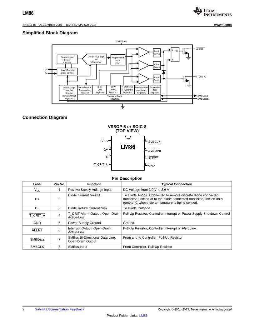
Control Logic
One Shot
Register
Remote Offset
Registers
Local/Remote
Temperature
Registers
HIGH
Limit
Registers
LOW
Limit
Registers
T_CRIT Limit
& Hysteresis
Registers
Configuration
and Status
Registers
Conversion
Rate
Registers
Two-Wire Serial
Interface
Local/Remote
Diode Selector
Temperature
Sensor
Circuitry
10-Bit Plus Sign'-6
Converter
Programable
Level
Filter
Fault
Queue
Fault
Queue
Fault
Queue
S
R
3.0V-3.6V
D+
D-
T_Crit_A
ALERT
SMBData
SMBClock
Q
LM86
SNIS114E –DECEMBER 2001–REVISED MARCH 2013 www.ti.com
Simplified Block Diagram
Connection Diagram
VSSOP-8 or SOIC-8(TOP VIEW)
Pin DescriptionLabel Pin No. Function Typical Connection
VDD 1 Positive Supply Voltage Input DC Voltage from 3.0 V to 3.6 V
Diode Current Source To Diode Anode. Connected to remote discrete diode connectedD+ 2 transistor junction or to the diode connected transistor junction on a
remote IC whose die temperature is being sensed.
D− 3 Diode Return Current Sink To Diode Cathode.
T_CRIT Alarm Output, Open-Drain, Pull-Up Resistor, Controller Interrupt or Power Supply Shutdown ControlT_CRIT_A 4 Active-Low
GND 5 Power Supply Ground Ground
Interrupt Output, Open-Drain, Pull-Up Resistor, Controller Interrupt or Alert LineALERT 6 Active-Low
SMBus Bi-Directional Data Line, From and to Controller, Pull-Up ResistorSMBData 7 Open-Drain Output
SMBCLK 8 SMBus Input From Controller, Pull-Up Resistor
2 Submit Documentation Feedback Copyright © 2001–2013, Texas Instruments Incorporated
Product Folder Links: LM86
LM86
www.ti.com SNIS114E –DECEMBER 2001–REVISED MARCH 2013
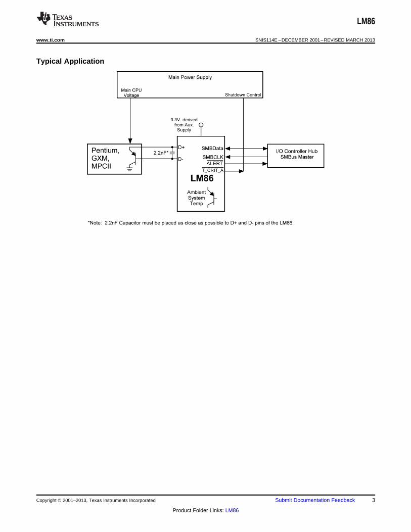
Typical Application
Copyright © 2001–2013, Texas Instruments Incorporated Submit Documentation Feedback 3
Product Folder Links: LM86

SNP
V+
GND
D1
D2
D4
D3R1
ESD
Clamp
D5
D6
I/O
LM86
SNIS114E –DECEMBER 2001–REVISED MARCH 2013 www.ti.com
These devices have limited built-in ESD protection. The leads should be shorted together or the device placed in conductive foamduring storage or handling to prevent electrostatic damage to the MOS gates.
Absolute Maximum Ratings (1)
Supply Voltage −0.3 V to 6.0 V
Voltage at SMBData, SMBCLK, ALERT, T_CRIT_A −0.5V to 6.0V
Voltage at Other Pins −0.3 V to (VDD + 0.3 V)
D− Input Current ±1 mA
Input Current at All Other Pins (2) ±5 mA
Package Input Current (2) 30 mA
SMBData, ALERT, T_CRIT_A Output Sink Current 10 mA
Storage Temperature −65°C to +150°C
Soldering Information, Lead Temperature, Vapor Phase (60 seconds) 215°CSOIC-8 or VSSOP-8 Packages (3)
Infrared (15 seconds) 220°C
ESD Susceptibility (4) Human Body Model 2000 V
Machine Model 200 V
(1) Absolute Maximum Ratings indicate limits beyond which damage to the device may occur. DC and AC electrical specifications do notapply when operating the device beyond its rated operating conditions.
(2) When the input voltage (VI) at any pin exceeds the power supplies (VI < GND or VI > VDD), the current at that pin should be limited to 5mA. Parasitic components and or ESD protection circuitry are shown in Table 1 and Figure 1 for the LM86's pins. The nominalbreakdown voltage of D3 is 6.5 V. Care should be taken not to forward bias the parasitic diode, D1, present on pins: D+, D−. Doing soby more than 50 mV may corrupt a temperature measurements.
(3) See the URL ”http://www.national.com/packaging/“ for other recommendations and methods of soldering surface mount devices.(4) Human body model, 100pF discharged through a 1.5kΩ resistor. Machine model, 200pF discharged directly into each pin.
Table 1. ESD Protection
Pin Name PIN D1 D2 D3 D4 D5 D6 R1 SNP ESDCLAM
P
VDD (V+) 1 x x
D+ 2 x (1) x x x x x
D− 3 x x x x x x
T_CRIT_A 4 x x x
ALERT 6 x x x
SMBData 7 x x x
SMBCLK 8 x
(1) An “x” indicates that the diode exists.
Figure 1. ESD Protection Input Structure
4 Submit Documentation Feedback Copyright © 2001–2013, Texas Instruments Incorporated
Product Folder Links: LM86

LM86
www.ti.com SNIS114E –DECEMBER 2001–REVISED MARCH 2013
Operating RatingsOperating Temperature Range 0°C to +125°C
Electrical Characteristics Temperature Range TMIN≤TA≤TMAX
LM86 0°C≤TA≤+85°C
Supply Voltage Range (VDD) +3.0V to +3.6V
Temperature-to-Digital Converter CharacteristicsUnless otherwise noted, these specifications apply for VDD=+3.0Vdc to 3.6Vdc. Boldface limits apply for TA = TJ =TMIN≤TA≤TMAX; all other limits TA= TJ=+25°C, unless otherwise noted.
Parameter Test Conditions Typical Limits Unit(1) (2) (Limit)
Temperature Accuracy Using Local Diode TA = +25°C to +125°C, (3) ±1 ±3 °C (max)
Temperature Accuracy Using Remote Diode of TA = +30°C TD = +80°C ±0.75 °C (max)mobile Pentium III with typical nonideality of 1.008. TA = +30°C to +50°C TD = +60°C to ±1 °C (max)For other processors email +100°[email protected] to obtain the
TA = +0°C to +85°C TD = +25°C to ±3 °C (max)latest data. (TD is the Remote Diode Junction+125°CTemperature)
Remote Diode Measurement Resolution 11 Bits
0.125 °C
Local Diode Measurement Resolution 8 Bits
1 °C
Conversion Time of All Temperatures at the Fastest (4) 31.25 34.4 ms (max)Setting
Quiescent Current (5) SMBus Inactive, 16Hz conversion rate 0.8 1.7 mA (max)
Shutdown 315 µA
D− Source Voltage 0.7 V
Diode Source Current (D+ − D−)=+ 0.65V; high level 160 315 µA (max)
110 µA (min)
Low level 13 20 µA (max)
7 µA (min)
ALERT and T_CRIT_A Output Saturation Voltage IOUT = 6.0 mA 0.4 V (max)
Power-On Reset Threshold Measure on VDD input, falling edge 2.4 V (max)1.8 V (min)
Local and Remote HIGH Default Temperature (6) +70 °Csettings
Local and Remote LOW Default Temperature (6) 0 °Csettings
Local and Remote T_CRIT Default Temperature (6) +85 °CSetting
(1) Typical values are at TA = 25°C and represent most likely parametric norm.(2) Limits are guaranteed to National's AOQL (Average Outgoing Quality Level).(3) Local temperature accuracy does not include the effects of self-heating. The rise in temperature due to self-heating is the product of the
internal power dissipation of the LM86 and the thermal resistance. See () for the thermal resistance to be used in the self-heatingcalculation.
(4) This specification is provided only to indicate how often temperature data is updated. The LM86 can be read at any time without regardto conversion state (and will yield last conversion result).
(5) Quiescent current will not increase substantially with an SMBus.(6) Default values set at power up.
Copyright © 2001–2013, Texas Instruments Incorporated Submit Documentation Feedback 5
Product Folder Links: LM86
LM86
SNIS114E –DECEMBER 2001–REVISED MARCH 2013 www.ti.com
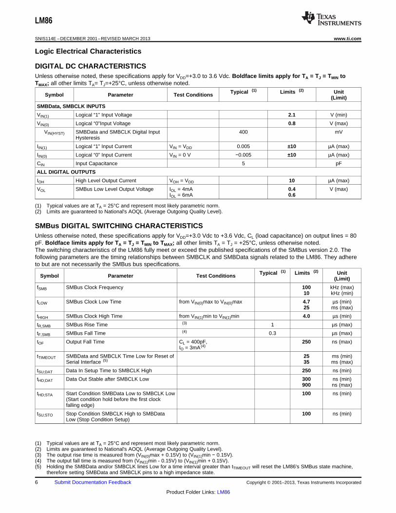
Logic Electrical Characteristics
DIGITAL DC CHARACTERISTICSUnless otherwise noted, these specifications apply for VDD=+3.0 to 3.6 Vdc. Boldface limits apply for TA = TJ = TMIN toTMAX; all other limits TA= TJ=+25°C, unless otherwise noted.
Typical (1) Limits (2) UnitSymbol Parameter Test Conditions (Limit)
SMBData, SMBCLK INPUTS
VIN(1) Logical “1” Input Voltage 2.1 V (min)
VIN(0) Logical “0”Input Voltage 0.8 V (max)
VIN(HYST) SMBData and SMBCLK Digital Input 400 mVHysteresis
IIN(1) Logical “1” Input Current VIN = VDD 0.005 ±10 µA (max)
IIN(0) Logical “0” Input Current VIN = 0 V −0.005 ±10 µA (max)
CIN Input Capacitance 5 pF
ALL DIGITAL OUTPUTS
IOH High Level Output Current VOH = VDD 10 µA (max)
VOL SMBus Low Level Output Voltage IOL = 4mA 0.4 V (max)IOL = 6mA 0.6
(1) Typical values are at TA = 25°C and represent most likely parametric norm.(2) Limits are guaranteed to National's AOQL (Average Outgoing Quality Level).
SMBus DIGITAL SWITCHING CHARACTERISTICSUnless otherwise noted, these specifications apply for VDD=+3.0 Vdc to +3.6 Vdc, CL (load capacitance) on output lines = 80pF. Boldface limits apply for TA = TJ = TMIN to TMAX; all other limits TA = TJ = +25°C, unless otherwise noted.The switching characteristics of the LM86 fully meet or exceed the published specifications of the SMBus version 2.0. Thefollowing parameters are the timing relationships between SMBCLK and SMBData signals related to the LM86. They adhereto but are not necessarily the SMBus bus specifications.
Typical (1) Limits (2) UnitSymbol Parameter Test Conditions (Limit)
fSMB SMBus Clock Frequency 100 kHz (max)10 kHz (min)
tLOW SMBus Clock Low Time from VIN(0)max to VIN(0)max 4.7 µs (min)25 ms (max)
tHIGH SMBus Clock High Time from VIN(1)min to VIN(1)min 4.0 µs (min)
tR,SMB SMBus Rise Time (3) 1 µs (max)
tF,SMB SMBus Fall Time (4) 0.3 µs (max)
tOF Output Fall Time CL = 400pF, 250 ns (max)IO = 3mA (4)
tTIMEOUT SMBData and SMBCLK Time Low for Reset of 25 ms (min)Serial Interface (5) 35 ms (max)
tSU;DAT Data In Setup Time to SMBCLK High 250 ns (min)
tHD;DAT Data Out Stable after SMBCLK Low 300 ns (min)900 ns (max)
tHD;STA Start Condition SMBData Low to SMBCLK Low 100 ns (min)(Start condition hold before the first clockfalling edge)
tSU;STO Stop Condition SMBCLK High to SMBData 100 ns (min)Low (Stop Condition Setup)
(1) Typical values are at TA = 25°C and represent most likely parametric norm.(2) Limits are guaranteed to National's AOQL (Average Outgoing Quality Level).(3) The output rise time is measured from (VIN(0)max + 0.15V) to (VIN(1)min − 0.15V).(4) The output fall time is measured from (VIN(1)min - 0.15V) to (VIN(1)min + 0.15V).(5) Holding the SMBData and/or SMBCLK lines Low for a time interval greater than tTIMEOUT will reset the LM86's SMBus state machine,
therefore setting SMBData and SMBCLK pins to a high impedance state.
6 Submit Documentation Feedback Copyright © 2001–2013, Texas Instruments Incorporated
Product Folder Links: LM86
VIH
VIL
SMBCLK
P
S
VIH
VI
L
SMBDAT
tBUFtHD;STA
tLOW
tR
tHD;DAT
tHIGH
tF
tSU;DATtSU;STA tSU;STO
P
LM86
www.ti.com SNIS114E –DECEMBER 2001–REVISED MARCH 2013
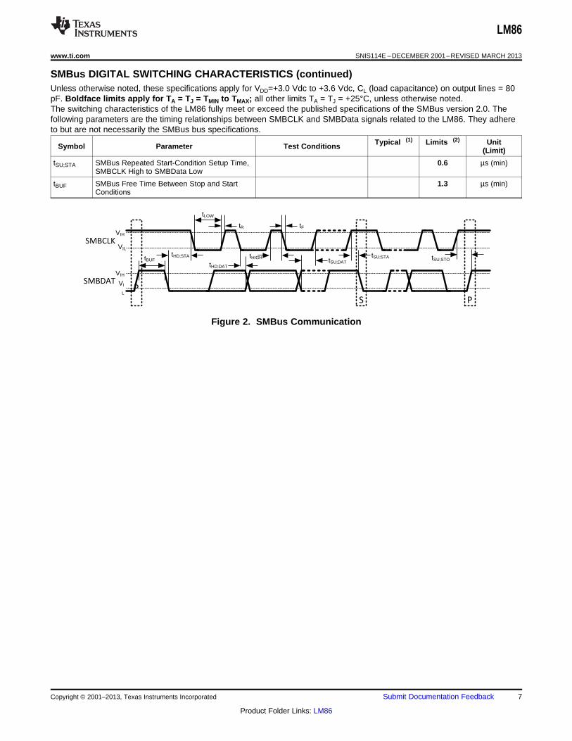
SMBus DIGITAL SWITCHING CHARACTERISTICS (continued)Unless otherwise noted, these specifications apply for VDD=+3.0 Vdc to +3.6 Vdc, CL (load capacitance) on output lines = 80pF. Boldface limits apply for TA = TJ = TMIN to TMAX; all other limits TA = TJ = +25°C, unless otherwise noted.The switching characteristics of the LM86 fully meet or exceed the published specifications of the SMBus version 2.0. Thefollowing parameters are the timing relationships between SMBCLK and SMBData signals related to the LM86. They adhereto but are not necessarily the SMBus bus specifications.
Typical (1) Limits (2) UnitSymbol Parameter Test Conditions (Limit)
tSU;STA SMBus Repeated Start-Condition Setup Time, 0.6 µs (min)SMBCLK High to SMBData Low
tBUF SMBus Free Time Between Stop and Start 1.3 µs (min)Conditions
Figure 2. SMBus Communication
Copyright © 2001–2013, Texas Instruments Incorporated Submit Documentation Feedback 7
Product Folder Links: LM86

0.01 0.1 1.0 10 100
CONVERSION RATE (Hz)
400
600
800
1000
1200
140
0
1600
1800
2000
SU
PP
LY C
UR
RE
NT
(P
A�
LM86
SNIS114E –DECEMBER 2001–REVISED MARCH 2013 www.ti.com
FUNCTIONAL DESCRIPTION
The LM86 temperature sensor incorporates a delta VBE based temperature sensor using a Local or Remotediode and a 10-bit plus sign ADC (Delta-Sigma Analog-to-Digital Converter). The LM86 is compatible with theserial SMBus version 2.0 two-wire interface. Digital comparators compare the measured Local Temperature (LT)to the Local High (LHS), Local Low (LLS) and Local T_CRIT (LCS) user-programmable temperature limitregisters. The measured Remote Temperature (RT) is digitally compared to the Remote High (RHS), RemoteLow (RLS) and Remote T_CRIT (RCS) user-programmable temperature limit registers. Activation of the ALERToutput indicates that a comparison is greater than the limit preset in a T_CRIT or HIGH limit register or less thanthe limit preset in a LOW limit register. The T_CRIT_A output responds as a true comparator with built inhysteresis. The hysteresis is set by the value placed in the Hysteresis register (TH). Activation of T_CRIT_Aoccurs when the temperature is above the T_CRIT setpoint. T_CRIT_A remains activated until the temperaturegoes below the setpoint calculated by T_CRIT − TH. The hysteresis register impacts both the remotetemperature and local temperature readings.
The LM86 may be placed in a low power consumption (Shutdown) mode by setting the RUN/STOP bit found inthe Configuration register. In the Shutdown mode, the LM86's SMBus interface remains while all circuitry notrequired is turned off.
The Local temperature reading and setpoint data registers are 8-bits wide. The format of the 11-bit remotetemperature data is a 16-bit left justified word. Two 8-bit registers, high and low bytes, are provided for eachsetpoint as well as the temperature reading. Two offset registers (RTOLB and RTOHB) can be used tocompensate for nonideality error. The remote temperature reading reported is adjusted by subtracting from oradding to the actual temperature reading the value placed in the offset registers.
CONVERSION SEQUENCE
The LM86 takes approximately 31.25 ms to convert the Local Temperature (LT), Remote Temperature (RT), andto update all of its registers. Only during the conversion process the busy bit (D7) in the Status register (02h) ishigh. These conversions are addressed in a round robin sequence. The conversion rate may be modified by theConversion Rate Register (04h). When the conversion rate is modified a delay is inserted between conversions,the actual conversion time remains at 31.25ms. Different conversion rates will cause the LM86 to draw differentamounts of supply current as shown in Figure 3.
Figure 3. Conversion Rate Effect on Power Supply Current
THE ALERT OUTPUT
The LM86's ALERT pin is an active-low open-drain output that is triggered by a temperature conversion that isoutside the limits defined by the temperature setpoint registers. Reset of the ALERT output is dependent uponthe selected method of use. The LM86's ALERT pin is versatile and will accommodate three different methods ofuse to best serve the system designer: as a temperature comparator, as a temperature based interrupt flag, andas part of an SMBus ALERT system. The three methods of use are further described below. The ALERT andinterrupt methods are different only in how the user interacts with the LM86.
8 Submit Documentation Feedback Copyright © 2001–2013, Texas Instruments Incorporated
Product Folder Links: LM86

Remote High Limit
RDTS Measurement
LM86 ALERT Pin
Status Register: RTDS High
TIME
TE
MP
ER
AT
UR
E
LM86
www.ti.com SNIS114E –DECEMBER 2001–REVISED MARCH 2013
Each temperature reading (LT and RT) is associated with a T_CRIT setpoint register (LCS, RCS), a HIGHsetpoint register (LHS and RHS) and a LOW setpoint register (LLS and RLS). At the end of every temperaturereading, a digital comparison determines whether that reading is above its HIGH or T_CRIT setpoint or below itsLOW setpoint. If so, the corresponding bit in the STATUS REGISTER is set. If the ALERT mask bit is not high,any bit set in the STATUS REGISTER, with the exception of Busy (D7) and OPEN (D2), will cause the ALERToutput to be pulled low. Any temperature conversion that is out of the limits defined by the temperature setpointregisters will trigger an ALERT. Additionally, the ALERT mask bit in the Configuration register must be cleared totrigger an ALERT in all modes.
ALERT Output as a Temperature Comparator
When the LM86 is implemented in a system in which it is not serviced by an interrupt routine, the ALERT outputcould be used as a temperature comparator. Under this method of use, once the condition that triggered theALERT to go low is no longer present, the ALERT is de-asserted (Figure 4). For example, if the ALERT outputwas activated by the comparison of LT > LHS, when this condition is no longer true the ALERT will return HIGH.This mode allows operation without software intervention, once all registers are configured during set-up. In orderfor the ALERT to be used as a temperature comparator, bit D0 (the ALERT configure bit) in the FILTER andALERT CONFIGURE REGISTER (xBF) must be set high. This is not the power on default state.
Figure 4. ALERT Comparator Temperature Response Diagram
ALERT Output as an Interrupt
The LM86's ALERT output can be implemented as a simple interrupt signal when it is used to trigger an interruptservice routine. In such systems it is undesirable for the interrupt flag to repeatedly trigger during or before theinterrupt service routine has been completed. Under this method of operation, during a read of the STATUSREGISTER the LM86 will set the ALERT mask bit (D7 of the Configuration register) if any bit in the STATUSREGISTER is set, with the exception of Busy (D7) and OPEN (D2). This prevents further ALERT triggering untilthe master has reset the ALERT mask bit, at the end of the interrupt service routine. The STATUS REGISTERbits are cleared only upon a read command from the master (see Figure 5) and will be re-asserted at the end ofthe next conversion if the triggering condition(s) persist(s). In order for the ALERT to be used as a dedicatedinterrupt signal, bit D0 (the ALERT configure bit) in the FILTER and ALERT CONFIGURE REGISTER (xBF) mustbe set low. This is the power on default state.
The following sequence describes the response of a system that uses the ALERT output pin as a interrupt flag:1. Master Senses ALERT low2. Master reads the LM86 STATUS REGISTER to determine what caused the ALERT3. LM86 clears STATUS REGISTER, resets the ALERT HIGH and sets the ALERT mask bit (D7 in the
Configuration register).4. Master attends to conditions that caused the ALERT to be triggered. The fan is started, setpoint limits are
adjusted, etc.5. Master resets the ALERT mask (D7 in the Configuration register).
Copyright © 2001–2013, Texas Instruments Incorporated Submit Documentation Feedback 9
Product Folder Links: LM86

Remote High LimitRDTS Measurement
TIMET
EM
PE
RA
TU
RE LM86 ALERT pin
Status Register: RTDS High
End of Temperature
conversion
ALERT mask set in
response to reading of
status register by
master
LM86
SNIS114E –DECEMBER 2001–REVISED MARCH 2013 www.ti.com
Figure 5. ALERT Output as an Interrupt Temperature Response Diagram
ALERT Output as an SMBus ALERT
When the ALERT output is connected to one or more ALERT outputs of other SMBus compatible devices and toa master, an SMBus alert line is created. Under this implementation, the LM86's ALERT should be operatedusing the ARA (Alert Response Address) protocol. The SMBus 2.0 ARA protocol, defined in the SMBusspecification 2.0, is a procedure designed to assist the master in resolving which part generated an interrupt andservice that interrupt while impeding system operation as little as possible.
The SMBus alert line is connected to the open-drain ports of all devices on the bus thereby AND'ing themtogether. The ARA is a method by which with one command the SMBus master may identify which part is pullingthe SMBus alert line LOW and prevent it from pulling it LOW again for the same triggering condition. When anARA command is received by all devices on the bus, the devices pulling the SMBus alert line LOW, first, sendtheir address to the master and second, release the SMBus alert line after recognizing a successful transmissionof their address.
The SMBus 1.1 and 2.0 specification state that in response to an ARA (Alert Response Address) “afteracknowledging the slave address the device must disengage its SMBALERT pulldown”. Furthermore, “if the hoststill sees SMBALERT low when the message transfer is complete, it knows to read the ARA again”. This SMBus“disengaging of SMBALERT” requirement prevents locking up the SMBus alert line. Competitive parts mayaddress this “disengaging of SMBALERT” requirement differently than the LM86 or not at all. SMBus systemsthat implement the ARA protocol as suggested for the LM86 will be fully compatible with all competitive parts.
The LM86 fulfills “disengaging of SMBALERT” by setting the ALERT mask bit (bit D7 in the Configurationregister, at address 09h) after successfully sending out its address in response to an ARA and releasing theALERT output pin. Once the ALERT mask bit is activated, the ALERT output pin will be disabled until enabled bysoftware. In order to enable the ALERT the master must read the STATUS REGISTER, at address 02h, duringthe interrupt service routine and then reset the ALERT mask bit in the Configuration register to 0 at the end ofthe interrupt service routine.
The following sequence describes the ARA response protocol.1. Master Senses SMBus alert line low2. Master sends a START followed by the Alert Response Address (ARA) with a Read Command.3. Alerting Device(s) send ACK.4. Alerting Device(s) send their Address. While transmitting their address, alerting devices sense whether their
address has been transmitted correctly. (The LM86 will reset its ALERT output and set the ALERT mask bitonce its complete address has been transmitted successfully.)
5. Master/slave NoACK6. Master sends STOP7. Master attends to conditions that caused the ALERT to be triggered. The STATUS REGISTER is read and
fan started, setpoint limits adjusted, etc.8. Master resets the ALERT mask (D7 in the Configuration register).
10 Submit Documentation Feedback Copyright © 2001–2013, Texas Instruments Incorporated
Product Folder Links: LM86

Remote High Limit
RDTS Measurement
TIME
TE
MP
ER
AT
UR
E
ALERT mask set in
response to ARA
from master
LM86 ALERT pin
Status Register: RTDS High
LM86
www.ti.com SNIS114E –DECEMBER 2001–REVISED MARCH 2013
The ARA, 000 1100, is a general call address. No device should ever be assigned this address.
Bit D0 (the ALERT configure bit) in the FILTER and ALERT CONFIGURE REGISTER (xBF) must be set low inorder for the LM86 to respond to the ARA command.
The ALERT output can be disabled by setting the ALERT mask bit, D7, of the Configuration register. The poweron default is to have the ALERT mask bit and the ALERT configure bit low.
Figure 6. ALERT Output as an SMBus ALERT Temperature Response Diagram
T_CRIT_A OUTPUT and T_CRIT LIMIT
T_CRIT_A is activated when any temperature reading is greater than the limit preset in the critical temperaturesetpoint register (T_CRIT), as shown in Figure 7. The Status Register can be read to determine which eventcaused the alarm. A bit in the Status Register is set high to indicate which temperature reading exceeded theT_CRIT setpoint temperature and caused the alarm, see STATUS REGISTER (SR).
Local and remote temperature diodes are sampled in sequence by the A/D converter. The T_CRIT_A output andthe Status Register flags are updated after every Local and Remote temperature conversion. T_CRT_A followsthe state of the comparison, it is reset when the temperature falls below the setpoint RCS-TH. The StatusRegister flags are reset only after the Status Register is read and if a temperature conversion(s) is/are below theT_CRIT setpoint, as shown in . Figure 7
Figure 7. T_CRIT_A Temperature Response Diagram
POWER ON RESET DEFAULT STATES
LM86 always powers up to these known default states. The LM86 remains in these states until after the firstconversion.1. Command Register set to 00h2. Local Temperature set to 0°C3. Remote Diode Temperature set to 0°C until the end of the first conversion.
Copyright © 2001–2013, Texas Instruments Incorporated Submit Documentation Feedback 11
Product Folder Links: LM86

LM86
SNIS114E –DECEMBER 2001–REVISED MARCH 2013 www.ti.com
4. Status Register set to 00h.5. Configuration register set to 00h; ALERT enabled, Remote T_CRIT alarm enabled and Local T_CRIT alarm
enabled6. 85°C Local and Remote T_CRIT temperature setpoints7. 70°C Local and Remote HIGH temperature setpoints8. 0°C Local and Remote LOW temperature setpoints9. Filter and Alert Configure Register set to 00h; filter disabled, ALERT output set as an SMBus ALERT10. Conversion Rate Register set to 8h; conversion rate set to 16 conv./sec.
SMBus INTERFACE
The LM86 operates as a slave on the SMBus, so the SMBCLK line is an input and the SMBData line is bi-directional. The LM86 never drives the SMBCLK line and it does not support clock stretching. According toSMBus specifications, the LM86 has a 7-bit slave address. All bits A6 through A0 are internally programmed andcan not be changed by software or hardware.
The complete slave address is:
A6 A5 A4 A3 A2 A1 A0
1 0 0 1 1 0 0
TEMPERATURE DATA FORMAT
Temperature data can only be read from the Local and Remote Temperature registers; the setpoint registers(T_CRIT, LOW, HIGH) are read/write.
Remote temperature data is represented by an 11-bit, two's complement word with an LSB (Least Significant Bit)equal to 0.125°C. The data format is a left justified 16-bit word available in two 8-bit registers:
Temperature Digital Output
Binary Hex
+125°C 0111 1101 0000 0000 7D00h
+25°C 0001 1001 0000 0000 1900h
+1°C 0000 0001 0000 0000 0100h
+0.125°C 0000 0000 0010 0000 0020h
0°C 0000 0000 0000 0000 0000h
−0.125°C 1111 1111 1110 0000 FFE0h
−1°C 1111 1111 0000 0000 FF00h
−25°C 1110 0111 0000 0000 E700h
−55°C 1100 1001 0000 0000 C900h
Local Temperature data is represented by an 8-bit, two's complement byte with an LSB (Least Significant Bit)equal to 1°C:
Temperature Digital Output
Binary Hex
+125°C 0111 1101 7Dh
+25°C 0001 1001 19h
+1°C 0000 0001 01h
0°C 0000 0000 00h
−1°C 1111 1111 FFh
−25°C 1110 0111 E7h
−55°C 1100 1001 C9h
12 Submit Documentation Feedback Copyright © 2001–2013, Texas Instruments Incorporated
Product Folder Links: LM86
LM86
www.ti.com SNIS114E –DECEMBER 2001–REVISED MARCH 2013
OPEN-DRAIN OUTPUTS
The SMBData, ALERT and T_CRIT_A outputs are open-drain outputs and do not have internal pull-ups. A “high”level will not be observed on these pins until pull-up current is provided by some external source, typically a pull-up resistor. Choice of resistor value depends on many system factors but, in general, the pull-up resistor shouldbe as large as possible. This will minimize any internal temperature reading errors due to internal heating of theLM86. The maximum resistance of the pull-up to provide a 2.1V high level, based on LM86 specification for HighLevel Output Current with the supply voltage at 3.0V, is 82kΩ(5%) or 88.7kΩ(1%).
DIODE FAULT DETECTION
The LM86 is equipped with operational circuitry designed to detect fault conditions concerning the remote diode.In the event that the D+ pin is detected as shorted to VDD or floating, the Remote Temperature High Byte (RTHB)register is loaded with +127°C, the Remote Temperature Low Byte (RTLB) register is loaded with 0, and theOPEN bit (D2) in the status register is set. As a result, if the Remote T_CRIT setpoint register (RCS) is set to avalue less than +127°C the ALERT and T_Crit output pins will be pulled low, if the Alert Mask and T_Crit Maskare disabled. If the Remote HIGH Setpoint High Byte Register (RHSHB) is set to a value less than +127°C thenALERT will be pulled low, if the Alert Mask is disabled. The OPEN bit itself will not trigger and ALERT.
In the event that the D+ pin is shorted to ground or D−, the Remote Temperature High Byte (RTHB) register isloaded with −128°C (1000 0000) and the OPEN bit (D2) in the status register will not be set. Since operating theLM86 at −128°C is beyond it's operational limits, this temperature reading represents this shorted fault condition.If the value in the Remote Low Setpoint High Byte Register (RLSHB) is more than −128°C and the Alert Mask isdisabled, ALERT will be pulled low.
Remote diode temperature sensors that have been previously released and are competitive with the LM86 outputa code of 0°C if the external diode is short-circuited. This change is an improvement that allows a reading of 0°Cto be truly interpreted as a genuine 0°C reading and not a fault condition.
COMMUNICATING WITH THE LM86
The data registers in the LM86 are selected by the Command Register. At power-up the Command Register isset to “00”, the location for the Read Local Temperature Register. The Command Register latches the lastlocation it was set to. Each data register in the LM86 falls into one of four types of user accessibility:1. Read only2. Write only3. Read/Write same address4. Read/Write different address
A Write to the LM86 will always include the address byte and the command byte. A write to any register requiresone data byte.
Reading the LM86 can take place either of two ways:1. If the location latched in the Command Register is correct (most of the time it is expected that the Command
Register will point to one of the Read Temperature Registers because that will be the data most frequentlyread from the LM86), then the read can simply consist of an address byte, followed by retrieving the databyte.
2. If the Command Register needs to be set, then an address byte, command byte, repeat start, and anotheraddress byte will accomplish a read.
The data byte has the most significant bit first. At the end of a read, the LM86 can accept either acknowledge orNo Acknowledge from the Master (No Acknowledge is typically used as a signal for the slave that the Master hasread its last byte). It takes the LM86 31.25ms to measure the temperature of the remote diode and internal diode.When retrieving all 10 bits from a previous remote diode temperature measurement, the master must insure thatall 10 bits are from the same temperature conversion. This may be achieved by using one-shot mode or bysetting the conversion rate and monitoring the busy bit such that no conversion occurs in between reading theMSB and LSB of the last temperature conversion.
Copyright © 2001–2013, Texas Instruments Incorporated Submit Documentation Feedback 13
Product Folder Links: LM86
LM86
SNIS114E –DECEMBER 2001–REVISED MARCH 2013 www.ti.com
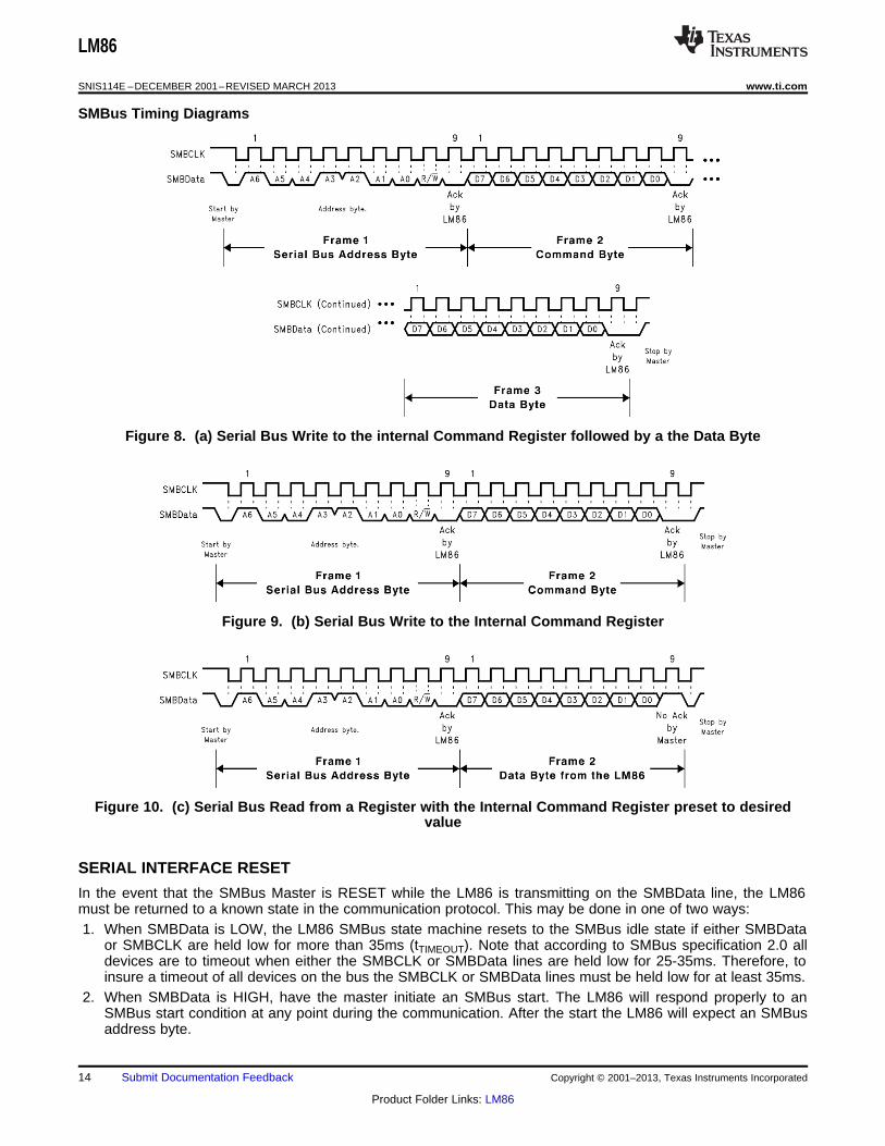
SMBus Timing Diagrams
Figure 8. (a) Serial Bus Write to the internal Command Register followed by a the Data Byte
Figure 9. (b) Serial Bus Write to the Internal Command Register
Figure 10. (c) Serial Bus Read from a Register with the Internal Command Register preset to desiredvalue
SERIAL INTERFACE RESET
In the event that the SMBus Master is RESET while the LM86 is transmitting on the SMBData line, the LM86must be returned to a known state in the communication protocol. This may be done in one of two ways:1. When SMBData is LOW, the LM86 SMBus state machine resets to the SMBus idle state if either SMBData
or SMBCLK are held low for more than 35ms (tTIMEOUT). Note that according to SMBus specification 2.0 alldevices are to timeout when either the SMBCLK or SMBData lines are held low for 25-35ms. Therefore, toinsure a timeout of all devices on the bus the SMBCLK or SMBData lines must be held low for at least 35ms.
2. When SMBData is HIGH, have the master initiate an SMBus start. The LM86 will respond properly to anSMBus start condition at any point during the communication. After the start the LM86 will expect an SMBusaddress byte.
14 Submit Documentation Feedback Copyright © 2001–2013, Texas Instruments Incorporated
Product Folder Links: LM86

25
27
29
31
33
35
37
39
41
43
45
0 50 100 150 200
SAMPLE NUMBER
TE
MP
ER
AT
UR
E (
o C)
LM86 with
Filter On
LM86 with
Filter Off
LM86
www.ti.com SNIS114E –DECEMBER 2001–REVISED MARCH 2013
DIGITAL FILTER
In order to suppress erroneous remote temperature readings due to noise, the LM86 incorporates a user-configured digital filter. The filter is accessed in the FILTER and ALERT CONFIGURE REGISTER at BFh. Thefilter can be set according to the following table.
D2 D1 Filter
0 0 No Filter
0 1 Level 1
1 0 Level 1
1 1 Level 2
Level 2 sets maximum filtering.
Figure 12 depict the filter output to in response to a step input and an impulse input. Figure 13 depicts the digitalfilter in use in a Pentium 4 processor system. Note that the two curves, with filter and without, have beenpurposely offset so that both responses can be clearly seen. Inserting the filter does not induce an offset asshown.
Figure 11. Filter Output Response to a Step Input Figure 12. Filter Output Response to a Step Inputa) Step Response b) Impulse Response
A. The filter on and off curves were purposely offset to better show noise performance.
Figure 13. Digital Filter Response in a Pentium 4 processor System
Copyright © 2001–2013, Texas Instruments Incorporated Submit Documentation Feedback 15
Product Folder Links: LM86
TE
MP
ER
AT
UR
E
n n+1 n+2 n+3 n+4 n+5
SAMPLE NUMBER
RDTS Measurement
Status Register: RTDS High
LM86
SNIS114E –DECEMBER 2001–REVISED MARCH 2013 www.ti.com
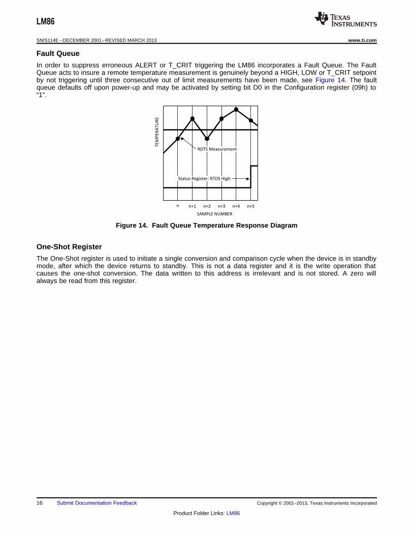
Fault Queue
In order to suppress erroneous ALERT or T_CRIT triggering the LM86 incorporates a Fault Queue. The FaultQueue acts to insure a remote temperature measurement is genuinely beyond a HIGH, LOW or T_CRIT setpointby not triggering until three consecutive out of limit measurements have been made, see Figure 14. The faultqueue defaults off upon power-up and may be activated by setting bit D0 in the Configuration register (09h) to“1”.
Figure 14. Fault Queue Temperature Response Diagram
One-Shot Register
The One-Shot register is used to initiate a single conversion and comparison cycle when the device is in standbymode, after which the device returns to standby. This is not a data register and it is the write operation thatcauses the one-shot conversion. The data written to this address is irrelevant and is not stored. A zero willalways be read from this register.
16 Submit Documentation Feedback Copyright © 2001–2013, Texas Instruments Incorporated
Product Folder Links: LM86
LM86
www.ti.com SNIS114E –DECEMBER 2001–REVISED MARCH 2013
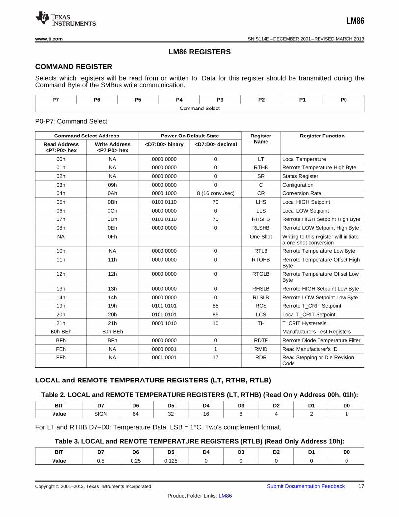
LM86 REGISTERS
COMMAND REGISTER
Selects which registers will be read from or written to. Data for this register should be transmitted during theCommand Byte of the SMBus write communication.
P7 P6 P5 P4 P3 P2 P1 P0
Command Select
P0-P7: Command Select
Command Select Address Power On Default State Register Register FunctionNameRead Address Write Address <D7:D0> binary <D7:D0> decimal
<P7:P0> hex <P7:P0> hex
00h NA 0000 0000 0 LT Local Temperature
01h NA 0000 0000 0 RTHB Remote Temperature High Byte
02h NA 0000 0000 0 SR Status Register
03h 09h 0000 0000 0 C Configuration
04h 0Ah 0000 1000 8 (16 conv./sec) CR Conversion Rate
05h 0Bh 0100 0110 70 LHS Local HIGH Setpoint
06h 0Ch 0000 0000 0 LLS Local LOW Setpoint
07h 0Dh 0100 0110 70 RHSHB Remote HIGH Setpoint High Byte
08h 0Eh 0000 0000 0 RLSHB Remote LOW Setpoint High Byte
NA 0Fh One Shot Writing to this register will initiatea one shot conversion
10h NA 0000 0000 0 RTLB Remote Temperature Low Byte
11h 11h 0000 0000 0 RTOHB Remote Temperature Offset HighByte
12h 12h 0000 0000 0 RTOLB Remote Temperature Offset LowByte
13h 13h 0000 0000 0 RHSLB Remote HIGH Setpoint Low Byte
14h 14h 0000 0000 0 RLSLB Remote LOW Setpoint Low Byte
19h 19h 0101 0101 85 RCS Remote T_CRIT Setpoint
20h 20h 0101 0101 85 LCS Local T_CRIT Setpoint
21h 21h 0000 1010 10 TH T_CRIT Hysteresis
B0h-BEh B0h-BEh Manufacturers Test Registers
BFh BFh 0000 0000 0 RDTF Remote Diode Temperature Filter
FEh NA 0000 0001 1 RMID Read Manufacturer's ID
FFh NA 0001 0001 17 RDR Read Stepping or Die RevisionCode
LOCAL and REMOTE TEMPERATURE REGISTERS (LT, RTHB, RTLB)
Table 2. LOCAL and REMOTE TEMPERATURE REGISTERS (LT, RTHB) (Read Only Address 00h, 01h):
BIT D7 D6 D5 D4 D3 D2 D1 D0
Value SIGN 64 32 16 8 4 2 1
For LT and RTHB D7–D0: Temperature Data. LSB = 1°C. Two's complement format.
Table 3. LOCAL and REMOTE TEMPERATURE REGISTERS (RTLB) (Read Only Address 10h):
BIT D7 D6 D5 D4 D3 D2 D1 D0
Value 0.5 0.25 0.125 0 0 0 0 0
Copyright © 2001–2013, Texas Instruments Incorporated Submit Documentation Feedback 17
Product Folder Links: LM86

LM86
SNIS114E –DECEMBER 2001–REVISED MARCH 2013 www.ti.com
For RTLB D7–D5: Temperature Data. LSB = 0.125°C. Two's complement format.
The maximum value available from the Local Temperature register is 127; the minimum value available from theLocal Temperature register is -128. The maximum value available from the Remote Temperature register is127.875; the minimum value available from the Remote Temperature registers is −128.875.
STATUS REGISTER (SR)
Table 4. STATUS REGISTER (SR) (Read Only Address 02h):
D7 D6 D5 D4 D3 D2 D1 D0
Busy LHIGH LLOW RHIGH RLOW OPEN RCRIT LCRIT
Power up default is with all bits “0” (zero).
D0: LCRIT: When set to “1” indicates a Local Critical Temperature alarm.
D1: RCRIT: When set to “1” indicates a Remote Diode Critical Temperature alarm.
D2: OPEN: When set to “1” indicates a Remote Diode disconnect.
D3: RLOW: When set to “1” indicates a Remote Diode LOW Temperature alarm
D4: RHIGH: When set to “1” indicates a Remote Diode HIGH Temperature alarm.
D5: LLOW: When set to “1” indicates a Local LOW Temperature alarm.
D6: LHIGH: When set to “1” indicates a Local HIGH Temperature alarm.
D7: Busy: When set to “1” ADC is busy converting.
CONFIGURATION REGISTER
Table 5. CONFIGURATION REGISTER (Read Address 03h /Write Address 09h):
D7 D6 D5 D4 D3 D2 D1 D0
ALERT mask RUN/STOP 0 Remote 0 Local 0 Fault QueueT_CRIT_A T_CRIT_A
mask mask
Power up default is with all bits “0” (zero)
D7: ALERT mask: When set to “1” ALERT interrupts are masked.
D6: RUN/STOP: When set to “1” SHUTDOWN is enabled.
D5: is not defined and defaults to “0”.
D4: Remote T_CRIT mask: When set to “1” a diode temperature reading that exceeds T_CRIT setpoint will notactivate the T_CRIT_A pin.
D3: is not defined and defaults to “0”.
D2: Local T_CRIT mask: When set to “1” a Local temperature reading that exceeds T_CRIT setpoint will notactivate the T_CRIT_A pin.
D1: is not defined and defaults to “0”.
D0: Fault Queue: when set to “1” three consecutive remote temperature measurements outside the HIGH, LOW,or T_CRIT setpoints will trigger an “Outside Limit” condition resulting in setting of status bits and associatedoutput pins..
18 Submit Documentation Feedback Copyright © 2001–2013, Texas Instruments Incorporated
Product Folder Links: LM86
LM86
www.ti.com SNIS114E –DECEMBER 2001–REVISED MARCH 2013
CONVERSION RATE REGISTER
Table 6. CONVERSION RATE REGISTER (ReadAddress 04h /Write Address 0Ah)
Value Conversion Rate
00 62.5 mHz
01 125 mHz
02 250 mHz
03 500 mHz
04 1 Hz
05 2 Hz
06 4 Hz
07 8 Hz
08 16 Hz
09 32 Hz
10-255 Undefined
LOCAL and REMOTE HIGH SETPOINT REGISTERS (LHS, RHSHB, and RHSLB)
Table 7. LOCAL and REMOTE HIGH SETPOINT REGISTERS (LHS, RHSHB) (Read Address 05h, 07h /WriteAddress 0Bh, 0Dh):
BIT D7 D6 D5 D4 D3 D2 D1 D0
Value SIGN 64 32 16 8 4 2 1
For LHS and RHSHB: HIGH setpoint temperature data. Power up default is LHIGH = RHIGH = 70°C. 1LSB =1°C. Two's complement format.
Table 8. LOCAL and REMOTE HIGH SETPOINT REGISTERS (RHSLB) (Read/Write Address 13h):
BIT D7 D6 D5 D4 D3 D2 D1 D0
Value 0.5 0.25 0.125 0 0 0 0 0
For RHSLB: Remote HIGH Setpoint Low Byte temperature data. Power up default is 0°C. 1LSB = 0.125°C.Two's complement format.
LOCAL and REMOTE LOW SETPOINT REGISTERS (LLS, RLSHB, and RLSLB)
Table 9. LOCAL and REMOTE LOW SETPOINT REGISTERS (LLS, RLSHB) (Read Address 06h, 08h, /WriteAddress 0Ch, 0Eh):
BIT D7 D6 D5 D4 D3 D2 D1 D0
Value SIGN 64 32 16 8 4 2 1
For LLS and RLSHB: HIGH setpoint temperature data. Power up default is LHIGH = RHIGH = 0°C. 1LSB = 1°C.Two's complement format.
Table 10. LOCAL and REMOTE LOW SETPOINT REGISTERS (RLSLB) (Read/Write Address 14h):
BIT D7 D6 D5 D4 D3 D2 D1 D0
Value 0.5 0.25 0.125 0 0 0 0 0
For RLSLB: Remote HIGH Setpoint Low Byte temperature data. Power up default is 0°C. 1LSB = 0.125°C. Two'scomplement format.
Copyright © 2001–2013, Texas Instruments Incorporated Submit Documentation Feedback 19
Product Folder Links: LM86

LM86
SNIS114E –DECEMBER 2001–REVISED MARCH 2013 www.ti.com
REMOTE TEMPERATURE OFFSET REGISTERS (RTOHB and RTOLB)
Table 11. REMOTE TEMPERATURE OFFSET REGISTERS (RTOHB) (Read/Write Address 11h):
BIT D7 D6 D5 D4 D3 D2 D1 D0
Value SIGN 64 32 16 8 4 2 1
For RTOHB: Remote Temperature Offset High Byte. Power up default is LHIGH = RHIGH = 0°C. 1LSB = 1°C.Two's complement format.
Table 12. REMOTE TEMPERATURE OFFSET REGISTERS (RTOLB) (Read/Write Address 12h):
BIT D7 D6 D5 D4 D3 D2 D1 D0
Value 0.5 0.25 0.125 0 0 0 0 0
For RTOLB: Remote Temperature Offset High Byte. Power up default is 0°C. 1LSB = 0.125°C. Two'scomplement format.
The offset value written to these registers will automatically be added to or subtracted from the remotetemperature measurement that will be reported in the Remote Temperature registers.
LOCAL and REMOTE T_CRIT REGISTERS (RCS and LCS)
Table 13. LOCAL and REMOTE T_CRIT REGISTERS (RCS and LCS) (Read/Write Address 20h, 19h):
BIT D7 D6 D5 D4 D3 D2 D1 D0
Value SIGN 64 32 16 8 4 2 1
D7–D0: T_CRIT setpoint temperature data. Power up default is T_CRIT = 85°C. 1 LSB = 1°C, two's complementformat.
T_CRIT HYSTERESIS REGISTER (TH)
Table 14. T_CRIT HYSTERESIS REGISTER (TH) (Read and Write Address 21h):
BIT D7 D6 D5 D4 D3 D2 D1 D0
Value 16 8 4 2 1
D7–D0: T_CRIT Hysteresis temperature. Power up default is TH = 10°C. 1 LSB = 1°C, maximum value = 31.
FILTER and ALERT CONFIGURE REGISTER
Table 15. FILTER and ALERT CONFIGURE REGISTER (Read and Write Address BFh):
BIT D7 D6 D5 D4 D3 D2 D1 D0
Value 0 0 0 0 0 Filter Level ALERT Configure
D7-D3: is not defined defaults to "0".
D2-D1: input filter setting as defined the table below:
D2 D1 Filter Level
0 0 No Filter
0 1 Level 1
1 0 Level 1
1 1 Level 2
20 Submit Documentation Feedback Copyright © 2001–2013, Texas Instruments Incorporated
Product Folder Links: LM86

LM86
www.ti.com SNIS114E –DECEMBER 2001–REVISED MARCH 2013
Level 2 sets maximum filtering.
D0: when set to "1" comparator mode is enabled.
MANUFACTURERS ID REGISTER
(Read Address FEh) Default value 01h.
DIE REVISION CODE REGISTER
(Read Address FFh) Default value 11hexadecimal or 17 decimal. This register will increment by 1 every timethere is a revision to the die by National Semiconductor.
Copyright © 2001–2013, Texas Instruments Incorporated Submit Documentation Feedback 21
Product Folder Links: LM86

Vt = k Tq
IF = IS e - 1
Vbe
KVt
LM86
SNIS114E –DECEMBER 2001–REVISED MARCH 2013 www.ti.com
APPLICATION HINTS
The LM86 can be applied easily in the same way as other integrated-circuit temperature sensors, and its remotediode sensing capability allows it to be used in new ways as well. It can be soldered to a printed circuit board,and because the path of best thermal conductivity is between the die and the pins, its temperature will effectivelybe that of the printed circuit board lands and traces soldered to the LM86's pins. This presumes that the ambientair temperature is almost the same as the surface temperature of the printed circuit board; if the air temperatureis much higher or lower than the surface temperature, the actual temperature of the of the LM86 die will be at anintermediate temperature between the surface and air temperatures. Again, the primary thermal conduction pathis through the leads, so the circuit board temperature will contribute to the die temperature much more stronglythan will the air temperature.
To measure temperature external to the LM86's die, use a remote diode. This diode can be located on the die ofa target IC, allowing measurement of the IC's temperature, independent of the LM86's temperature. The LM86has been optimized to measure the remote diode of a Pentium III processor as shown in Figure 15. A discretediode can also be used to sense the temperature of external objects or ambient air. Remember that a discretediode's temperature will be affected, and often dominated, by the temperature of its leads.
Figure 15. Mobile Pentium III or 3904 Temperature vs LM86 Temperature Reading
Most silicon diodes do not lend themselves well to this application. It is recommended that a 2N3904 transistorbase emitter junction be used with the collector tied to the base.
A diode connected 2N3904 approximates the junction available on a Pentium III microprocessor for temperaturemeasurement. Therefore, the LM86 can sense the temperature of this diode effectively.
DIODE NONIDEALITY
Diode Nonideality Factor Effect on Accuracy
When a transistor is connected as a diode, the following relationship holds for variables VBE, T and If:
(1)
where:
(2)
• q = 1.6×10⁻¹⁹ Coulombs (the electron charge),• T = Absolute Temperature in Kelvin• k = 1.38×10⁻²³joules/K (Boltzmann's constant),• η is the nonideality factor of the process the diode is manufactured on,• IS = Saturation Current and is process dependent,• If= Forward Current through the base emitter junction• VBE = Base Emitter Voltage drop
In the active region, the -1 term is negligible and may be eliminated, yielding the following equation
22 Submit Documentation Feedback Copyright © 2001–2013, Texas Instruments Incorporated
Product Folder Links: LM86

Vbe = K ln (N) k Tq
IF = IS e
Vbe
KVt
LM86
www.ti.com SNIS114E –DECEMBER 2001–REVISED MARCH 2013
(3)
In the above equation, η and IS are dependant upon the process that was used in the fabrication of the particulardiode. By forcing two currents with a very controlled ration (N) and measuring the resulting voltage difference, itis possible to eliminate the IS term. Solving for the forward voltage difference yields the relationship:
(4)
The nonideality factor, η, is the only other parameter not accounted for and depends on the diode that is used formeasurement. Since ΔVBE is proportional to both η and T, the variations in η cannot be distinguished fromvariations in temperature. Since the nonideality factor is not controlled by the temperature sensor, it will directlyadd to the inaccuracy of the sensor. For the Pentium III Intel specifies a ±1% variation in η from part to part. Asan example, assume a temperature sensor has an accuracy specification of ±1°C at room temperature of 25 °Cand the process used to manufacture the diode has a nonideality variation of ±1%. The resulting accuracy of thetemperature sensor at room temperature will be:
TACC = ± 1°C + (±1% of 298 °K) = ±4 °C (5)
The additional inaccuracy in the temperature measurement caused by η, can be eliminated if each temperaturesensor is calibrated with the remote diode that it will be paired with. The following table shows the variations innonideality for a variety of processors.
Processor Family η, nonideality
min typ max
Pentium II 1 1.0065 1.0173
Pentium III CPUID 67h 1 1.0065 1.0125
Pentium III CPUID 68h/PGA370Socket/Celeron 1.0057 1.008 1.0125
Pentium 4, 423 pin 0.9933 1.0045 1.0368
Pentium 4, 478 pin 0.9933 1.0045 1.0368
MMBT3904 1.003
AMD Athlon MP model 6 1.002 1.008 1.016
Compensating for Diode Nonideality
In order to compensate for the errors introduced by nonideality, the temperature sensor is calibrated for aparticular processor. National Semiconductor temperature sensors are always calibrated to the typical nonidealityof a given processor type. The LM86 is calibrated for the nonideality of a mobile Pentium III processor, 1.008.When a temperature sensor calibrated for a particular processor type is used with a different processor type or agiven processor type has a nonideality that strays from the typical, errors are introduced. Figure 16 shows theminimum and maximum errors introduced to a temperature sensor calibrated specifically to the typical value ofthe processor type it is connected to. The errors in this figure are attributed only to the variation in nonidealityfrom the typical value. In Figure 17 is a plot of the errors that result from using a temperature sensor calibratedfor a Pentium II, the LM84, with a typical Pentium 4 or AMD Athlon MP Model 6.
Copyright © 2001–2013, Texas Instruments Incorporated Submit Documentation Feedback 23
Product Folder Links: LM86

-0.4-0.35
-0.3-0.25
-0.2-0.15
-0.1-0.05
0.050.1
0.150.2
0.250.3
0.350.4
-60 -40 -20 0 20 40 60 80
TEMPERATURE (oC)
0
TE
MP
ER
AT
UR
E S
HIF
T (
o C)
100 120 140
n_ideality =1.008
using LM84.
n_ideality =1.0045
using LM84.
-6
-4
-2
0
2
4
6
8
10
12
14
-60 -40 -20 0 20 40 60 80 100 120 140
TEMPERATURE (oC)
ER
RO
R (
o C)
Pentium 4
Pentium III CPUID 68h/Celeron
Pentium 4
Pentium II
n_ideality =1.008
using LM84.
n_ideality =1.008
using LM86.
n_ideality =1.0045
using LM84.
TEMPERATURE (°C)
TE
MP
ER
AT
UR
E S
HIF
T (
°C)
-1
-0.8
-0.6
-0.4
-0.2
0
0.2
0.4
0.6
0.8
1
-60 -40 -20 0 20 40 60 80 100 120 140
LM86
SNIS114E –DECEMBER 2001–REVISED MARCH 2013 www.ti.com
Figure 16. Error Caused by Nonideality Factor Figure 17. Errors Induced when TemperatureSensor is Not Calibrated to Typical Nonideality
Figure 18. Compensating for an Untargeted Nonideality Factor
Temperature errors associated with nonideality may be reduced in a specific temperature range of concernthrough use of the offset registers (11h and 12h). Figure 18 shows how the offset register may be used tocompensate for the nonideality errors shown in Figure 17. For the case of nonideality=1.008, the offset registerwas set to −0.5°C resulting in the calculated residual error as shown in Figure 18. This offset has resulted in anerror of less than 0.05°C for the temperatures measured in the critical range between 60 to 100°C. This methodyields a first order correction factor.
Please send an email to [email protected] requesting further information on our recommendedsetting of the offset register for different processor types.
PCB LAYOUT FOR MINIMIZING NOISE
Figure 19. Ideal Diode Trace Layout
24 Submit Documentation Feedback Copyright © 2001–2013, Texas Instruments Incorporated
Product Folder Links: LM86
LM86
www.ti.com SNIS114E –DECEMBER 2001–REVISED MARCH 2013
In a noisy environment, such as a processor mother board, layout considerations are very critical. Noise inducedon traces running between the remote temperature diode sensor and the LM86 can cause temperatureconversion errors. Keep in mind that the signal level the LM86 is trying to measure is in microvolts. The followingguidelines should be followed:1. Place a 0.1 µF power supply bypass capacitor as close as possible to the VDDpin and the recommended 2.2
nF capacitor as close as possible to the LM86's D+ and D− pins. Make sure the traces to the 2.2nF capacitorare matched.
2. The recommended 2.2nF diode bypass capacitor actually has a range of TBDpF to 3.3nF. The averagetemperature accuracy will not degrade. Increasing the capacitance will lower the corner frequency wheredifferential noise error affects the temperature reading thus producing a reading that is more stable.Conversely, lowering the capacitance will increase the corner frequency where differential noise error affectsthe temperature reading thus producing a reading that is less stable.
3. Ideally, the LM86 should be placed within 10cm of the Processor diode pins with the traces being as straight,short and identical as possible. Trace resistance of 1Ω can cause as much as 1°C of error. This error can becompensated by using the Remote Temperature Offset Registers, since the value placed in these registerswill automatically be subtracted from or added to the remote temperature reading.
4. Diode traces should be surrounded by a GND guard ring to either side, above and below if possible. ThisGND guard should not be between the D+ and D− lines. In the event that noise does couple to the diodelines it would be ideal if it is coupled common mode. That is equally to the D+ and D− lines.
5. Avoid routing diode traces in close proximity to power supply switching or filtering inductors.6. Avoid running diode traces close to or parallel to high speed digital and bus lines. Diode traces should be
kept at least 2cm apart from the high speed digital traces.7. If it is necessary to cross high speed digital traces, the diode traces and the high speed digital traces should
cross at a 90 degree angle.8. The ideal place to connect the LM86's GND pin is as close as possible to the Processors GND associated
with the sense diode.9. Leakage current between D+ and GND should be kept to a minimum. One nano-ampere of leakage can
cause as much as 1°C of error in the diode temperature reading. Keeping the printed circuit board as cleanas possible will minimize leakage current.
Noise coupling into the digital lines greater than 400mVp-p (typical hysteresis) and undershoot less than 500mVbelow GND, may prevent successful SMBus communication with the LM86. SMBus no acknowledge is the mostcommon symptom, causing unnecessary traffic on the bus. Although the SMBus maximum frequency ofcommunication is rather low (100kHz max), care still needs to be taken to ensure proper termination within asystem with multiple parts on the bus and long printed circuit board traces. An RC lowpass filter with a 3dbcorner frequency of about 40MHz is included on the LM86's SMBCLK input. Additional resistance can be addedin series with the SMBData and SMBCLK lines to further help filter noise and ringing. Minimize noise coupling bykeeping digital traces out of switching power supply areas as well as ensuring that digital lines containing highspeed data communications cross at right angles to the SMBData and SMBCLK lines.
Copyright © 2001–2013, Texas Instruments Incorporated Submit Documentation Feedback 25
Product Folder Links: LM86
LM86
SNIS114E –DECEMBER 2001–REVISED MARCH 2013 www.ti.com
DATA SHEET REVISION HISTORY
Date Revision
4/2003 1. Added improved guaranteed Temperature Error specification for the Remote Diode Readings of ±0.75ºC to page 1and Electrical Characteristics.
2. in DIE REVISION CODE REGISTER changed "21h" to "11hexadecimal or 17 decimal"
3. Changed numbering of "Applications Hints" from "4." to "3."
4. Added "Data Sheet Revision History" section.
3/2013 Changed layout of National Data Sheet to TI format
26 Submit Documentation Feedback Copyright © 2001–2013, Texas Instruments Incorporated
Product Folder Links: LM86

PACKAGE OPTION ADDENDUM
www.ti.com 14-Oct-2017
Addendum-Page 1
PACKAGING INFORMATION
Orderable Device Status(1)
Package Type PackageDrawing
Pins PackageQty
Eco Plan(2)
Lead/Ball Finish(6)
MSL Peak Temp(3)
Op Temp (°C) Device Marking(4/5)
Samples
LM86CIM NRND SOIC D 8 95 TBD Call TI Call TI 0 to 125 LM86CIM
LM86CIM/NOPB ACTIVE SOIC D 8 95 Green (RoHS& no Sb/Br)
CU SN Level-1-260C-UNLIM 0 to 125 LM86CIM
LM86CIMM NRND VSSOP DGK 8 1000 TBD Call TI Call TI 0 to 125 T10C
LM86CIMM/NOPB ACTIVE VSSOP DGK 8 1000 Green (RoHS& no Sb/Br)
CU SN Level-1-260C-UNLIM 0 to 125 T10C
LM86CIMMX/NOPB ACTIVE VSSOP DGK 8 3500 Green (RoHS& no Sb/Br)
CU SN Level-1-260C-UNLIM 0 to 125 T10C
LM86CIMX/NOPB ACTIVE SOIC D 8 2500 Green (RoHS& no Sb/Br)
CU SN Level-1-260C-UNLIM 0 to 125 LM86CIM
(1) The marketing status values are defined as follows:ACTIVE: Product device recommended for new designs.LIFEBUY: TI has announced that the device will be discontinued, and a lifetime-buy period is in effect.NRND: Not recommended for new designs. Device is in production to support existing customers, but TI does not recommend using this part in a new design.PREVIEW: Device has been announced but is not in production. Samples may or may not be available.OBSOLETE: TI has discontinued the production of the device.
(2) RoHS: TI defines "RoHS" to mean semiconductor products that are compliant with the current EU RoHS requirements for all 10 RoHS substances, including the requirement that RoHS substancedo not exceed 0.1% by weight in homogeneous materials. Where designed to be soldered at high temperatures, "RoHS" products are suitable for use in specified lead-free processes. TI mayreference these types of products as "Pb-Free".RoHS Exempt: TI defines "RoHS Exempt" to mean products that contain lead but are compliant with EU RoHS pursuant to a specific EU RoHS exemption.Green: TI defines "Green" to mean the content of Chlorine (Cl) and Bromine (Br) based flame retardants meet JS709B low halogen requirements of <=1000ppm threshold. Antimony trioxide basedflame retardants must also meet the <=1000ppm threshold requirement.
(3) MSL, Peak Temp. - The Moisture Sensitivity Level rating according to the JEDEC industry standard classifications, and peak solder temperature.
(4) There may be additional marking, which relates to the logo, the lot trace code information, or the environmental category on the device.
(5) Multiple Device Markings will be inside parentheses. Only one Device Marking contained in parentheses and separated by a "~" will appear on a device. If a line is indented then it is a continuationof the previous line and the two combined represent the entire Device Marking for that device.
(6) Lead/Ball Finish - Orderable Devices may have multiple material finish options. Finish options are separated by a vertical ruled line. Lead/Ball Finish values may wrap to two lines if the finishvalue exceeds the maximum column width.
PACKAGE OPTION ADDENDUM
www.ti.com 14-Oct-2017
Addendum-Page 2
Important Information and Disclaimer:The information provided on this page represents TI's knowledge and belief as of the date that it is provided. TI bases its knowledge and belief on informationprovided by third parties, and makes no representation or warranty as to the accuracy of such information. Efforts are underway to better integrate information from third parties. TI has taken andcontinues to take reasonable steps to provide representative and accurate information but may not have conducted destructive testing or chemical analysis on incoming materials and chemicals.TI and TI suppliers consider certain information to be proprietary, and thus CAS numbers and other limited information may not be available for release.
In no event shall TI's liability arising out of such information exceed the total purchase price of the TI part(s) at issue in this document sold by TI to Customer on an annual basis.

TAPE AND REEL INFORMATION
*All dimensions are nominal
Device PackageType
PackageDrawing
Pins SPQ ReelDiameter
(mm)
ReelWidth
W1 (mm)
A0(mm)
B0(mm)
K0(mm)
P1(mm)
W(mm)
Pin1Quadrant
LM86CIMM VSSOP DGK 8 1000 178.0 12.4 5.3 3.4 1.4 8.0 12.0 Q1
LM86CIMM/NOPB VSSOP DGK 8 1000 178.0 12.4 5.3 3.4 1.4 8.0 12.0 Q1
LM86CIMMX/NOPB VSSOP DGK 8 3500 330.0 12.4 5.3 3.4 1.4 8.0 12.0 Q1
LM86CIMX/NOPB SOIC D 8 2500 330.0 12.4 6.5 5.4 2.0 8.0 12.0 Q1
PACKAGE MATERIALS INFORMATION
www.ti.com 24-Aug-2017
Pack Materials-Page 1

*All dimensions are nominal
Device Package Type Package Drawing Pins SPQ Length (mm) Width (mm) Height (mm)
LM86CIMM VSSOP DGK 8 1000 210.0 185.0 35.0
LM86CIMM/NOPB VSSOP DGK 8 1000 210.0 185.0 35.0
LM86CIMMX/NOPB VSSOP DGK 8 3500 367.0 367.0 35.0
LM86CIMX/NOPB SOIC D 8 2500 367.0 367.0 35.0
PACKAGE MATERIALS INFORMATION
www.ti.com 24-Aug-2017
Pack Materials-Page 2


IMPORTANT NOTICE
Texas Instruments Incorporated (TI) reserves the right to make corrections, enhancements, improvements and other changes to itssemiconductor products and services per JESD46, latest issue, and to discontinue any product or service per JESD48, latest issue. Buyersshould obtain the latest relevant information before placing orders and should verify that such information is current and complete.TI’s published terms of sale for semiconductor products (http://www.ti.com/sc/docs/stdterms.htm) apply to the sale of packaged integratedcircuit products that TI has qualified and released to market. Additional terms may apply to the use or sale of other types of TI products andservices.Reproduction of significant portions of TI information in TI data sheets is permissible only if reproduction is without alteration and isaccompanied by all associated warranties, conditions, limitations, and notices. TI is not responsible or liable for such reproduceddocumentation. Information of third parties may be subject to additional restrictions. Resale of TI products or services with statementsdifferent from or beyond the parameters stated by TI for that product or service voids all express and any implied warranties for theassociated TI product or service and is an unfair and deceptive business practice. TI is not responsible or liable for any such statements.Buyers and others who are developing systems that incorporate TI products (collectively, “Designers”) understand and agree that Designersremain responsible for using their independent analysis, evaluation and judgment in designing their applications and that Designers havefull and exclusive responsibility to assure the safety of Designers' applications and compliance of their applications (and of all TI productsused in or for Designers’ applications) with all applicable regulations, laws and other applicable requirements. Designer represents that, withrespect to their applications, Designer has all the necessary expertise to create and implement safeguards that (1) anticipate dangerousconsequences of failures, (2) monitor failures and their consequences, and (3) lessen the likelihood of failures that might cause harm andtake appropriate actions. Designer agrees that prior to using or distributing any applications that include TI products, Designer willthoroughly test such applications and the functionality of such TI products as used in such applications.TI’s provision of technical, application or other design advice, quality characterization, reliability data or other services or information,including, but not limited to, reference designs and materials relating to evaluation modules, (collectively, “TI Resources”) are intended toassist designers who are developing applications that incorporate TI products; by downloading, accessing or using TI Resources in anyway, Designer (individually or, if Designer is acting on behalf of a company, Designer’s company) agrees to use any particular TI Resourcesolely for this purpose and subject to the terms of this Notice.TI’s provision of TI Resources does not expand or otherwise alter TI’s applicable published warranties or warranty disclaimers for TIproducts, and no additional obligations or liabilities arise from TI providing such TI Resources. TI reserves the right to make corrections,enhancements, improvements and other changes to its TI Resources. TI has not conducted any testing other than that specificallydescribed in the published documentation for a particular TI Resource.Designer is authorized to use, copy and modify any individual TI Resource only in connection with the development of applications thatinclude the TI product(s) identified in such TI Resource. NO OTHER LICENSE, EXPRESS OR IMPLIED, BY ESTOPPEL OR OTHERWISETO ANY OTHER TI INTELLECTUAL PROPERTY RIGHT, AND NO LICENSE TO ANY TECHNOLOGY OR INTELLECTUAL PROPERTYRIGHT OF TI OR ANY THIRD PARTY IS GRANTED HEREIN, including but not limited to any patent right, copyright, mask work right, orother intellectual property right relating to any combination, machine, or process in which TI products or services are used. Informationregarding or referencing third-party products or services does not constitute a license to use such products or services, or a warranty orendorsement thereof. Use of TI Resources may require a license from a third party under the patents or other intellectual property of thethird party, or a license from TI under the patents or other intellectual property of TI.TI RESOURCES ARE PROVIDED “AS IS” AND WITH ALL FAULTS. TI DISCLAIMS ALL OTHER WARRANTIES ORREPRESENTATIONS, EXPRESS OR IMPLIED, REGARDING RESOURCES OR USE THEREOF, INCLUDING BUT NOT LIMITED TOACCURACY OR COMPLETENESS, TITLE, ANY EPIDEMIC FAILURE WARRANTY AND ANY IMPLIED WARRANTIES OFMERCHANTABILITY, FITNESS FOR A PARTICULAR PURPOSE, AND NON-INFRINGEMENT OF ANY THIRD PARTY INTELLECTUALPROPERTY RIGHTS. TI SHALL NOT BE LIABLE FOR AND SHALL NOT DEFEND OR INDEMNIFY DESIGNER AGAINST ANY CLAIM,INCLUDING BUT NOT LIMITED TO ANY INFRINGEMENT CLAIM THAT RELATES TO OR IS BASED ON ANY COMBINATION OFPRODUCTS EVEN IF DESCRIBED IN TI RESOURCES OR OTHERWISE. IN NO EVENT SHALL TI BE LIABLE FOR ANY ACTUAL,DIRECT, SPECIAL, COLLATERAL, INDIRECT, PUNITIVE, INCIDENTAL, CONSEQUENTIAL OR EXEMPLARY DAMAGES INCONNECTION WITH OR ARISING OUT OF TI RESOURCES OR USE THEREOF, AND REGARDLESS OF WHETHER TI HAS BEENADVISED OF THE POSSIBILITY OF SUCH DAMAGES.Unless TI has explicitly designated an individual product as meeting the requirements of a particular industry standard (e.g., ISO/TS 16949and ISO 26262), TI is not responsible for any failure to meet such industry standard requirements.Where TI specifically promotes products as facilitating functional safety or as compliant with industry functional safety standards, suchproducts are intended to help enable customers to design and create their own applications that meet applicable functional safety standardsand requirements. Using products in an application does not by itself establish any safety features in the application. Designers mustensure compliance with safety-related requirements and standards applicable to their applications. Designer may not use any TI products inlife-critical medical equipment unless authorized officers of the parties have executed a special contract specifically governing such use.Life-critical medical equipment is medical equipment where failure of such equipment would cause serious bodily injury or death (e.g., lifesupport, pacemakers, defibrillators, heart pumps, neurostimulators, and implantables). Such equipment includes, without limitation, allmedical devices identified by the U.S. Food and Drug Administration as Class III devices and equivalent classifications outside the U.S.TI may expressly designate certain products as completing a particular qualification (e.g., Q100, Military Grade, or Enhanced Product).Designers agree that it has the necessary expertise to select the product with the appropriate qualification designation for their applicationsand that proper product selection is at Designers’ own risk. Designers are solely responsible for compliance with all legal and regulatoryrequirements in connection with such selection.Designer will fully indemnify TI and its representatives against any damages, costs, losses, and/or liabilities arising out of Designer’s non-compliance with the terms and provisions of this Notice.
Mailing Address: Texas Instruments, Post Office Box 655303, Dallas, Texas 75265Copyright © 2017, Texas Instruments Incorporated


![[XLS]specials.indiatoday.comspecials.indiatoday.com/aajtaknew/pdf/L92200DL1999PLC... · Web view1267748.75 0 0 0 0 0 0 0 0.75 0.75 0.75 0.75 0.75 0.75 0.75 0.75 0.75 0.75 12.75 0.75](https://img.pdfslide.us/doc/110x75/5aa92ca27f8b9a72188c8ae6/xls-view126774875-0-0-0-0-0-0-0-075-075-075-075-075-075-075-075-075.jpg)