Embed Size (px)
Citation preview
VLSI Design : Chapter 5-1 1
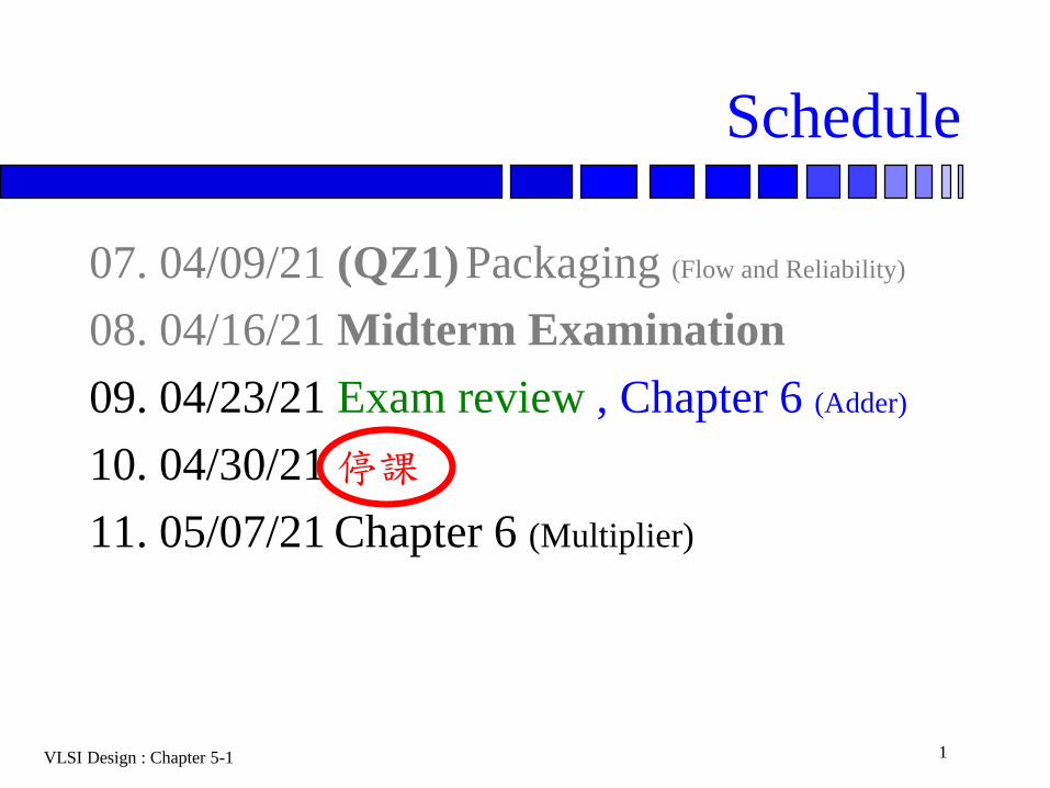
Schedule
07. 04/09/21 (QZ1) Packaging (Flow and Reliability)
08. 04/16/21 Midterm Examination
09. 04/23/21 Exam review , Chapter 6 (Adder)
10. 04/30/21 停課
11. 05/07/21 Chapter 6 (Multiplier)
VLSI Design : Chapter 5-1 2
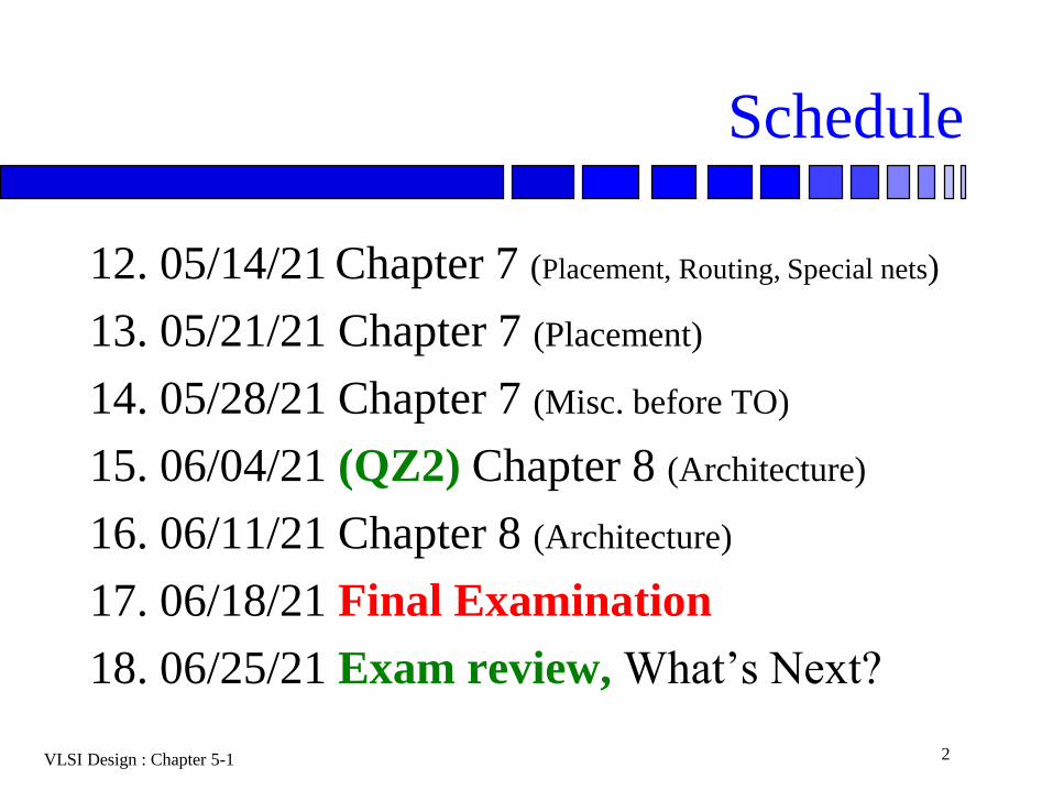
Schedule
12. 05/14/21 Chapter 7 (Placement, Routing, Special nets)
13. 05/21/21 Chapter 7 (Placement)
14. 05/28/21 Chapter 7 (Misc. before TO)
15. 06/04/21 (QZ2) Chapter 8 (Architecture)
16. 06/11/21 Chapter 8 (Architecture)
17. 06/18/21 Final Examination
18. 06/25/21 Exam review, What’s Next?
VLSI Design: Chapter 6-1 3
Design Flow
Design flow is not fixed. It depends on the design application, technologies, company resources….and the most important, design managers…
Design flow will be shown in Chapter 9 again, we explain it tonight and will revisit it weeks later.
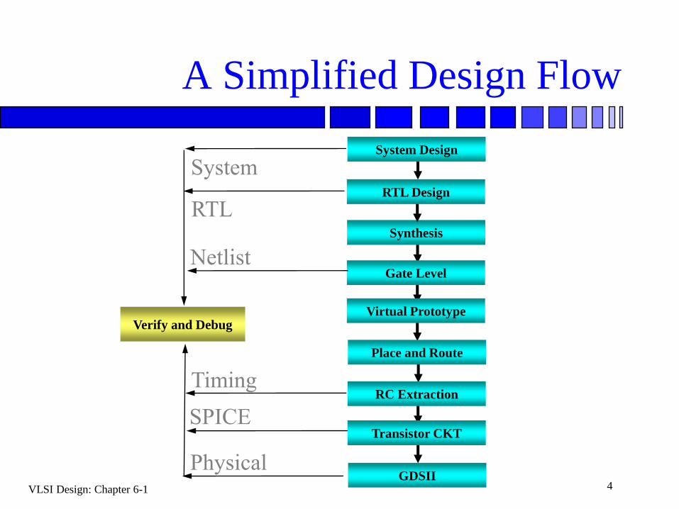
VLSI Design: Chapter 6-1 4
A Simplified Design Flow
System Design
Verify and Debug
Synthesis
Gate Level
Virtual Prototype
Place and Route
RC Extraction
Transistor CKT
GDSII
RTL Design
System
RTL
Netlist
Timing
Physical
SPICE
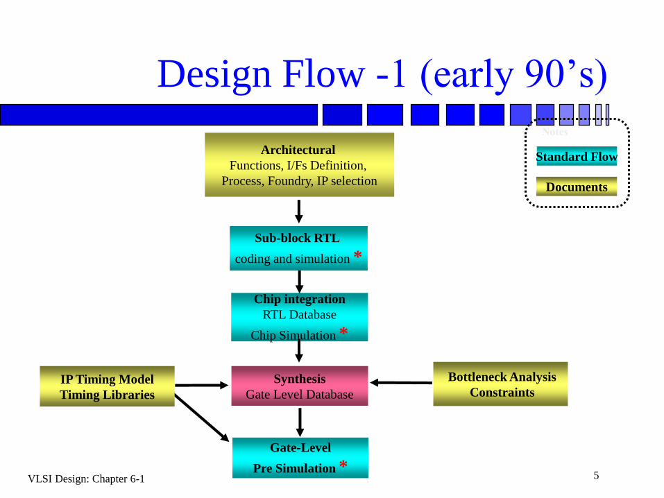
VLSI Design: Chapter 6-1 5
Design Flow -1 (early 90’s)
Chip integration
RTL Database
Chip Simulation *
Bottleneck Analysis
Constraints
Sub-block RTL
coding and simulation *
IP Timing Model
Timing Libraries
Architectural
Functions, I/Fs Definition,
Process, Foundry, IP selection
Gate-Level
Pre Simulation *
Documents
Standard Flow
Notes
Synthesis
Gate Level Database
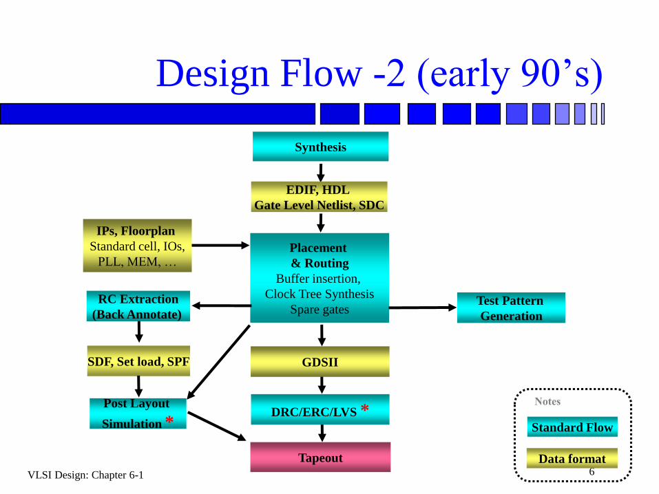
VLSI Design: Chapter 6-1 6
Design Flow -2 (early 90’s)
Data format
Standard Flow
Notes
Placement
& Routing
Buffer insertion,
Clock Tree Synthesis
Spare gates
EDIF, HDL
Gate Level Netlist, SDC
IPs, Floorplan
Standard cell, IOs,
PLL, MEM, …
SDF, Set load, SPF
RC Extraction
(Back Annotate)
Synthesis
Post Layout
Simulation *
Test Pattern
Generation
Tapeout
DRC/ERC/LVS *
GDSII
VLSI Design: Chapter 6-1 7
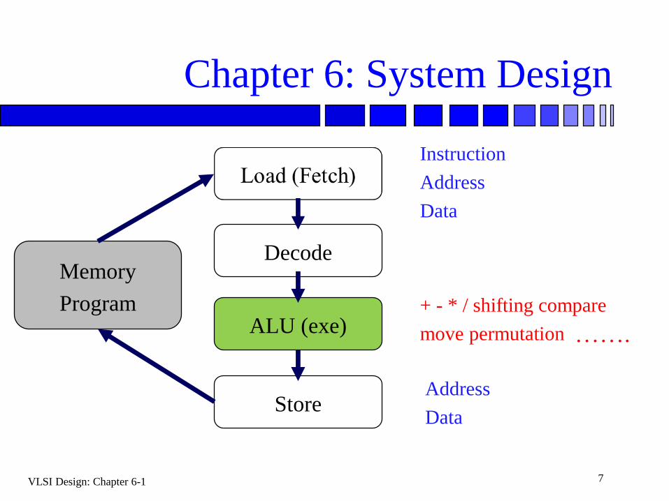
Chapter 6: System Design
Memory
Program
Decode
ALU (exe)
Store
Instruction
Address
Data
Address
Data
+ - * / shifting compare
move permutation …….
VLSI Design: Chapter 6-1 8
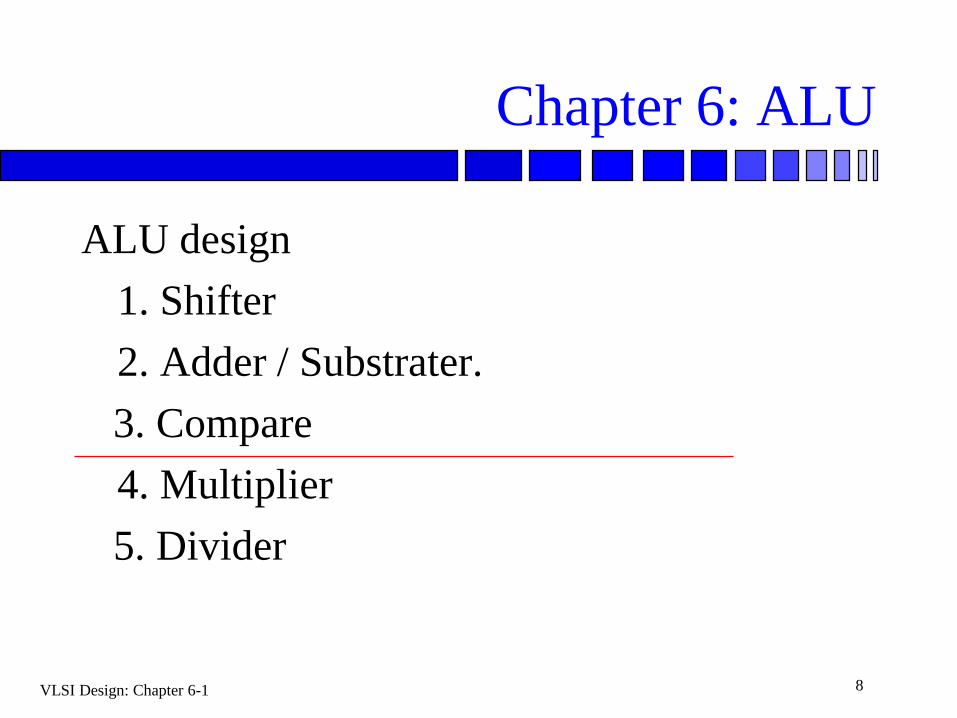
Chapter 6: ALU
ALU design
1. Shifter
2. Adder / Substrater.
3. Compare
4. Multiplier
5. Divider
VLSI Design: Chapter 6-1 9
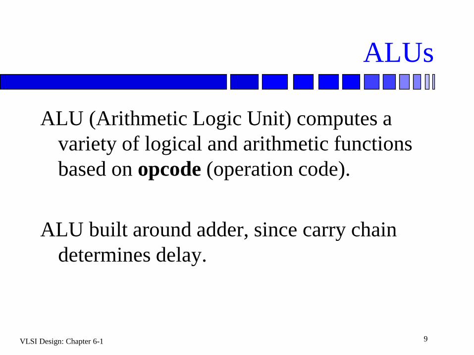
ALUs
ALU (Arithmetic Logic Unit) computes a
variety of logical and arithmetic functions
based on opcode (operation code).
ALU built around adder, since carry chain
determines delay.
VLSI Design: Chapter 6-1 10
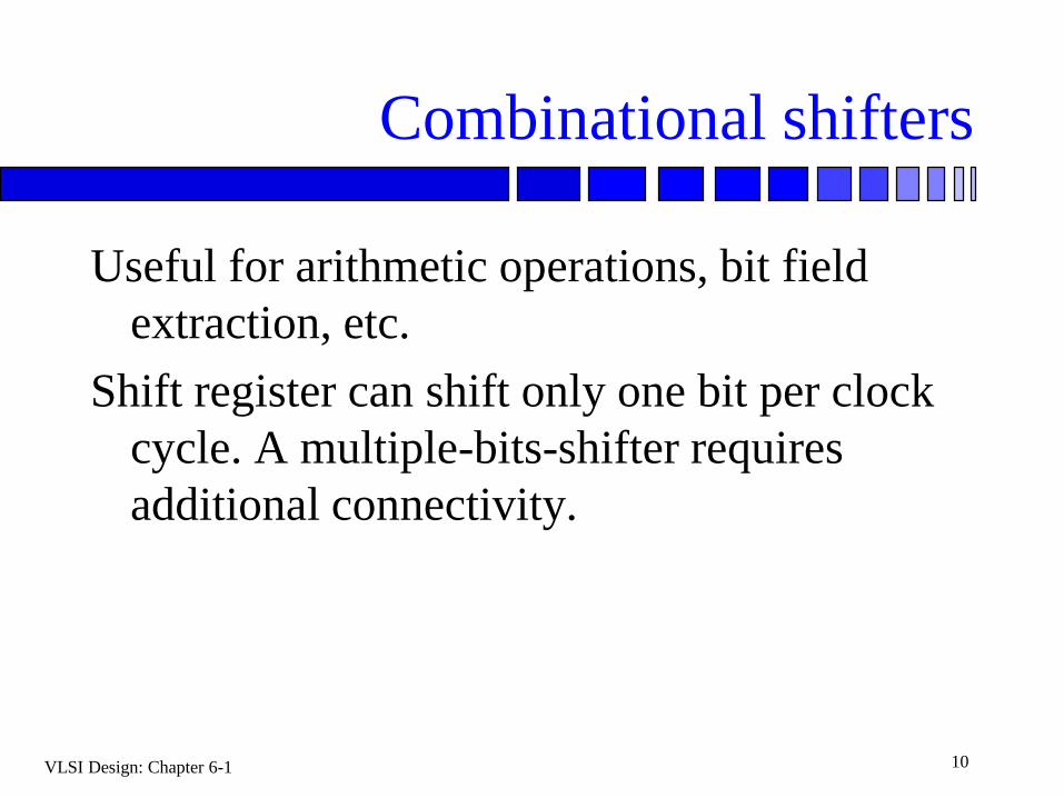
Combinational shifters
Useful for arithmetic operations, bit field
extraction, etc.
Shift register can shift only one bit per clock
cycle. A multiple-bits-shifter requires
additional connectivity.
VLSI Design: Chapter 6-1 11
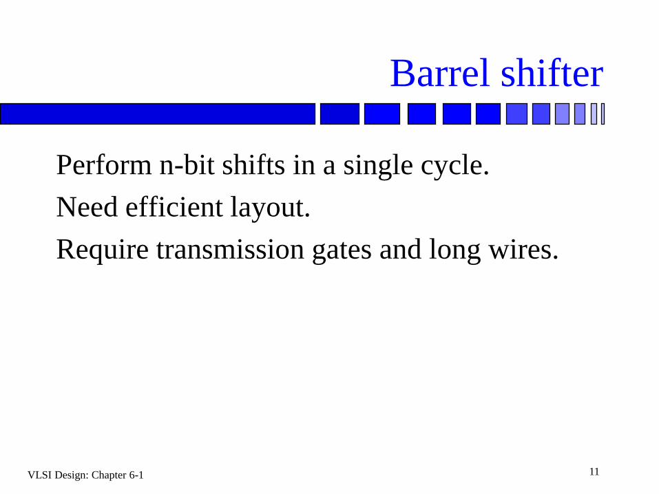
Barrel shifter
Perform n-bit shifts in a single cycle.
Need efficient layout.
Require transmission gates and long wires.
VLSI Design: Chapter 6-1 12
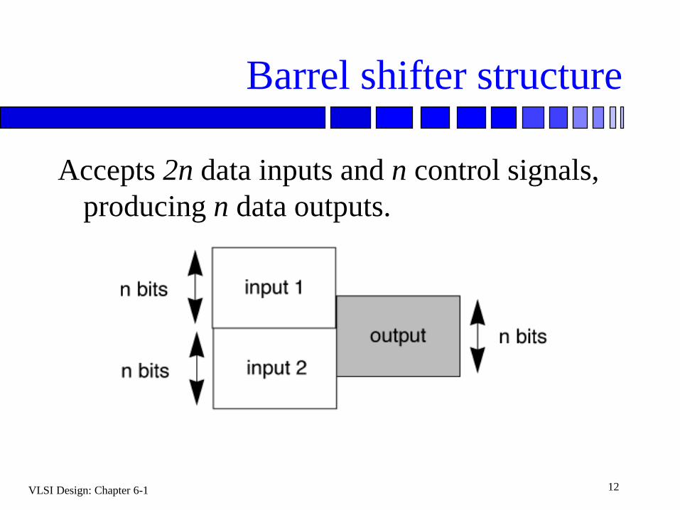
Barrel shifter structure
Accepts 2n data inputs and n control signals,
producing n data outputs.
VLSI Design: Chapter 6-1 13
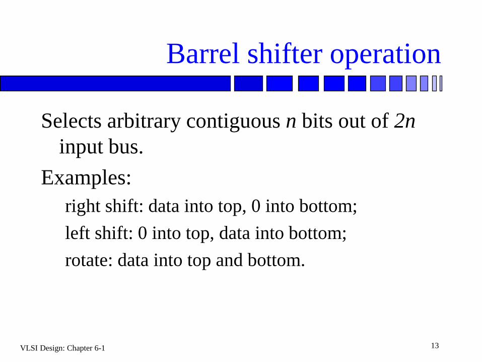
Barrel shifter operation
Selects arbitrary contiguous n bits out of 2n
input bus.
Examples:
right shift: data into top, 0 into bottom;
left shift: 0 into top, data into bottom;
rotate: data into top and bottom.
VLSI Design: Chapter 6-1 14
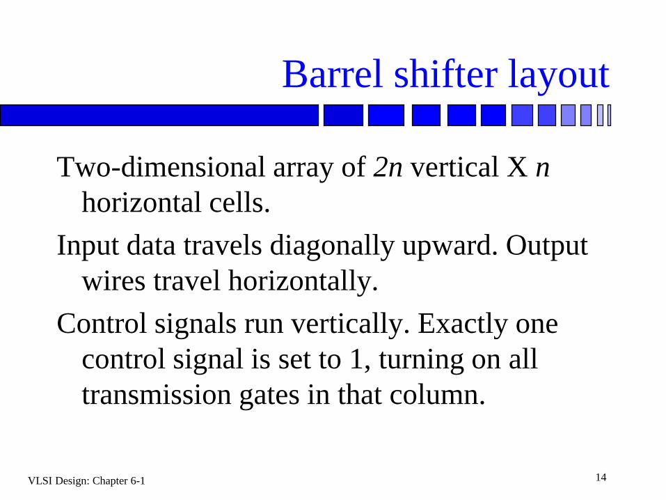
Barrel shifter layout
Two-dimensional array of 2n vertical X n
horizontal cells.
Input data travels diagonally upward. Output
wires travel horizontally.
Control signals run vertically. Exactly one
control signal is set to 1, turning on all
transmission gates in that column.
VLSI Design: Chapter 6-1 15
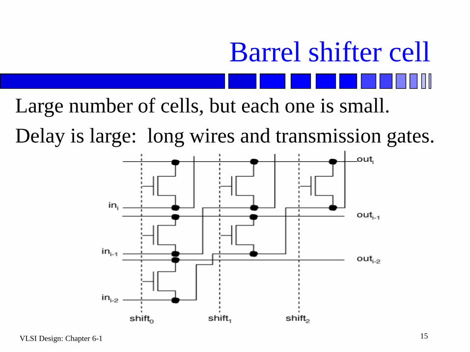
Barrel shifter cell
Large number of cells, but each one is small.
Delay is large: long wires and transmission gates.
VLSI Design: Chapter 6-1 16
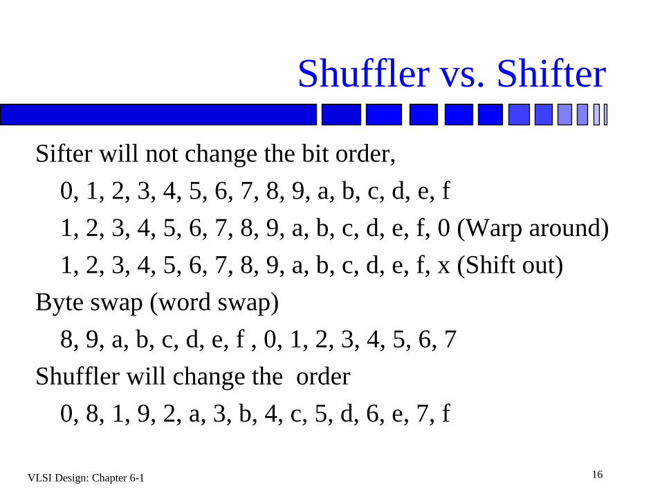
Shuffler vs. Shifter
Sifter will not change the bit order,
0, 1, 2, 3, 4, 5, 6, 7, 8, 9, a, b, c, d, e, f
1, 2, 3, 4, 5, 6, 7, 8, 9, a, b, c, d, e, f, 0 (Warp around)
1, 2, 3, 4, 5, 6, 7, 8, 9, a, b, c, d, e, f, x (Shift out)
Byte swap (word swap)
8, 9, a, b, c, d, e, f , 0, 1, 2, 3, 4, 5, 6, 7
Shuffler will change the order
0, 8, 1, 9, 2, a, 3, b, 4, c, 5, d, 6, e, 7, f
VLSI Design: Chapter 6-1 17
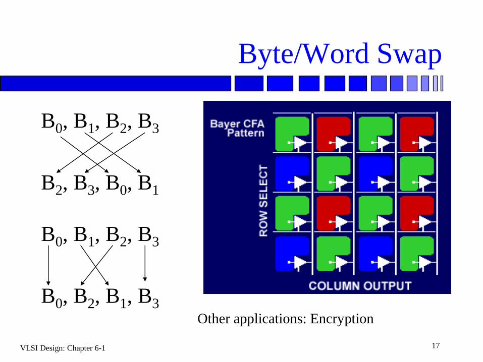
Byte/Word Swap
B0, B1, B2, B3
B2, B3, B0, B1
B0, B1, B2, B3
B0, B2, B1, B3Other applications: Encryption
VLSI Design: Chapter 6-1 18
2. Adders
Adder delay is dominated by carry.
Carry chain analysis must consider transistor,
wiring delay.
Modern VLSI favors adder designs which
have compact carry chains.
VLSI Design: Chapter 6-1 19
Most common adders
Serial adder
Ripple adder
Carry Look Ahead adder (CLA)
Carry Skip adder
Carry Select adder
VLSI Design: Chapter 6-1 20
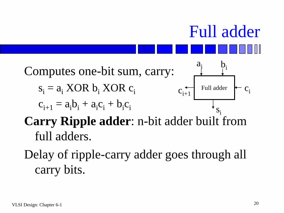
Full adder
Computes one-bit sum, carry:
si = ai XOR bi XOR ci
ci+1 = aibi + aici + bici
Carry Ripple adder: n-bit adder built from
full adders.
Delay of ripple-carry adder goes through all
carry bits.
ai bi
ci
si
ci+1Full adder
VLSI Design: Chapter 6-1 21
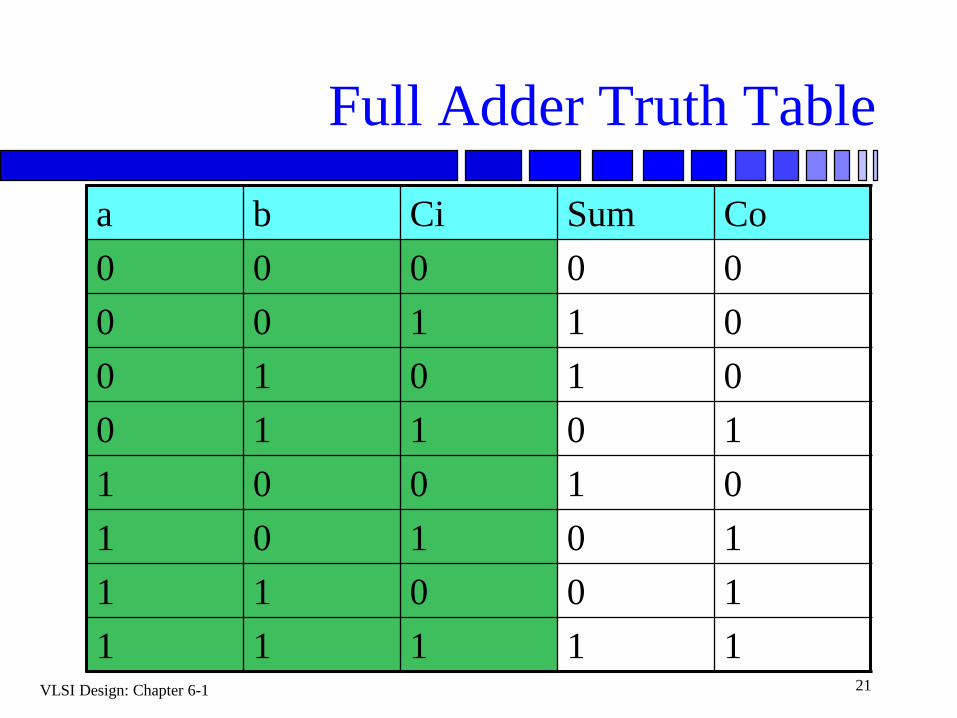
Full Adder Truth Table
a b Ci Sum Co
0 0 0 0 0
0 0 1 1 0
0 1 0 1 0
0 1 1 0 1
1 0 0 1 0
1 0 1 0 1
1 1 0 0 1
1 1 1 1 1
VLSI Design: Chapter 6-1 22
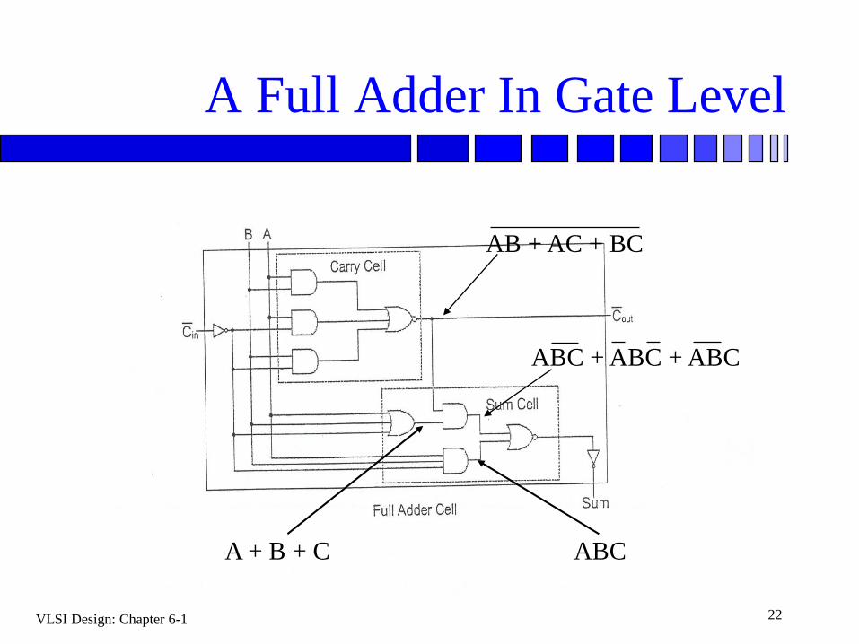
A Full Adder In Gate Level
AB + AC + BC
ABC + ABC + ABC
A + B + C ABC
VLSI Design: Chapter 6-1 23
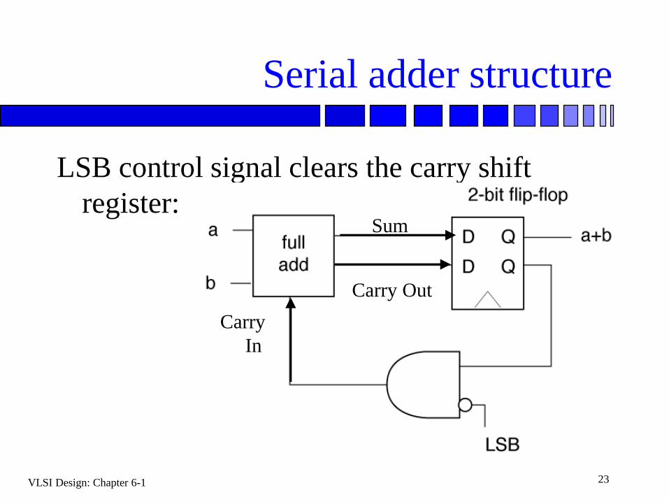
Serial adder structure
LSB control signal clears the carry shift
register:
Carry Out
Sum
Carry
In
VLSI Design: Chapter 6-1 24
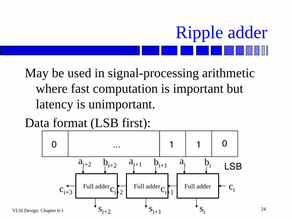
Ripple adder
May be used in signal-processing arithmetic
where fast computation is important but
latency is unimportant.
Data format (LSB first):
ai bi
ci
si
ci+1Full adder
ai+1
si+1
bi+1
ci+2Full adder
ai+2
si+2
bi+2
ci+3Full adder
VLSI Design: Chapter 6-1 25
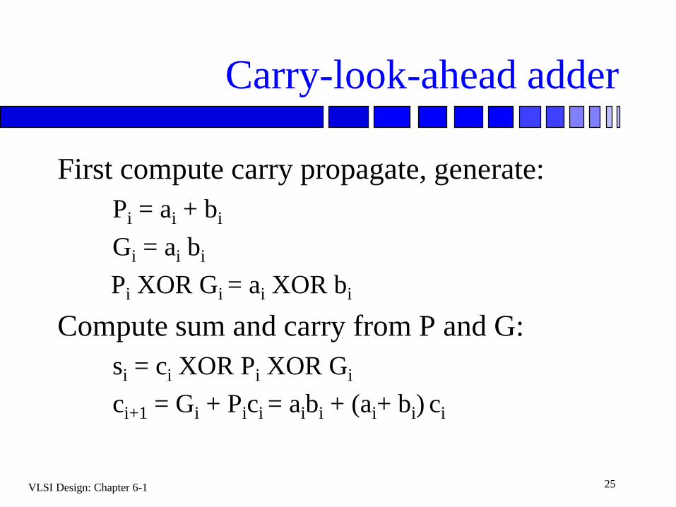
Carry-look-ahead adder
First compute carry propagate, generate:
Pi = ai + bi
Gi = ai bi
Pi XOR Gi = ai XOR bi
Compute sum and carry from P and G:
si = ci XOR Pi XOR Gi
ci+1 = Gi + Pici = aibi + (ai+ bi) ci
VLSI Design: Chapter 6-1 26
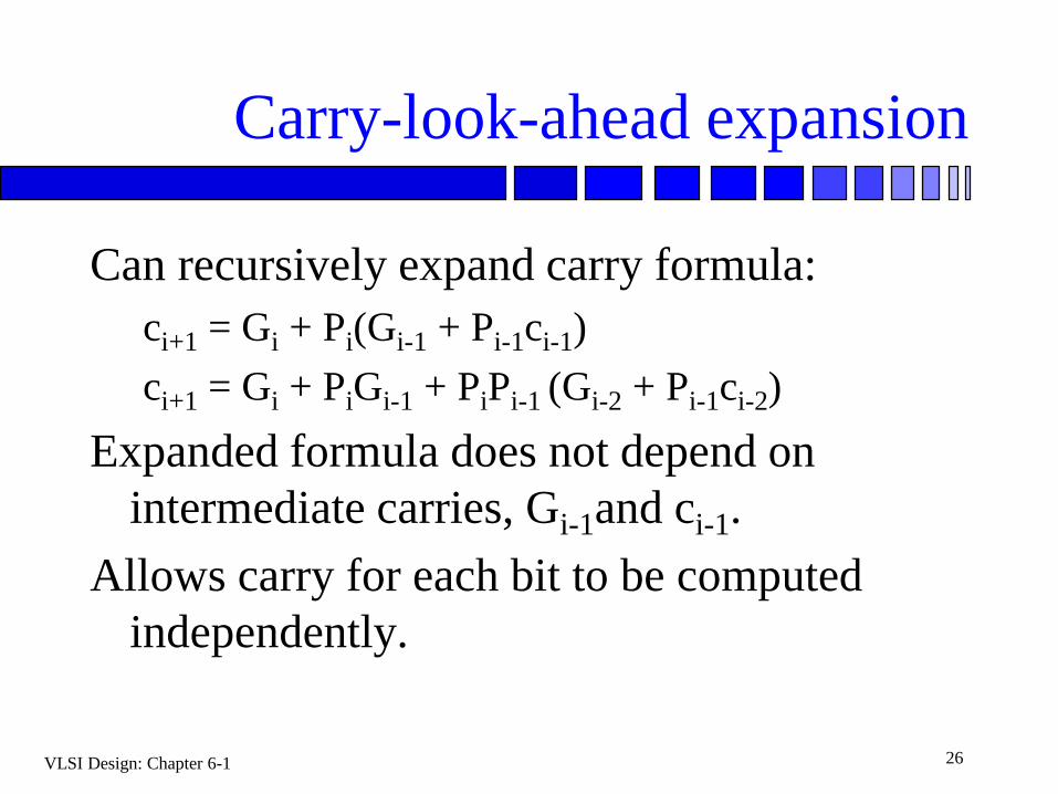
Carry-look-ahead expansion
Can recursively expand carry formula:
ci+1 = Gi + Pi(Gi-1 + Pi-1ci-1)
ci+1 = Gi + PiGi-1 + PiPi-1 (Gi-2 + Pi-1ci-2)
Expanded formula does not depend on
intermediate carries, Gi-1and ci-1.
Allows carry for each bit to be computed
independently.
VLSI Design: Chapter 6-1 27
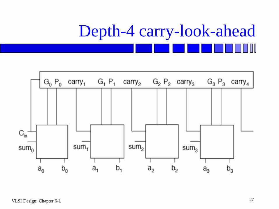
Depth-4 carry-look-ahead
VLSI Design: Chapter 6-1 28
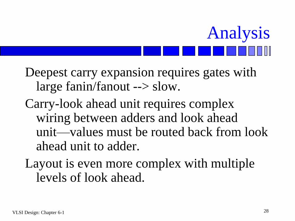
Analysis
Deepest carry expansion requires gates with large fanin/fanout --> slow.
Carry-look ahead unit requires complex wiring between adders and look ahead unit—values must be routed back from look ahead unit to adder.
Layout is even more complex with multiple levels of look ahead.
VLSI Design: Chapter 6-1 29
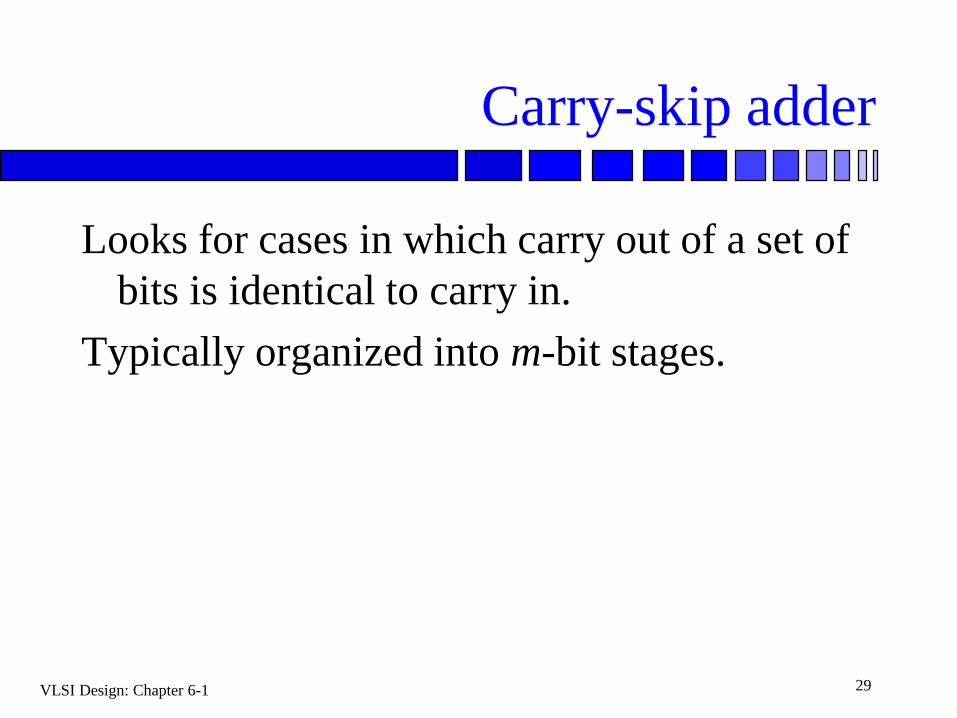
Carry-skip adder
Looks for cases in which carry out of a set of
bits is identical to carry in.
Typically organized into m-bit stages.
VLSI Design: Chapter 6-1 30
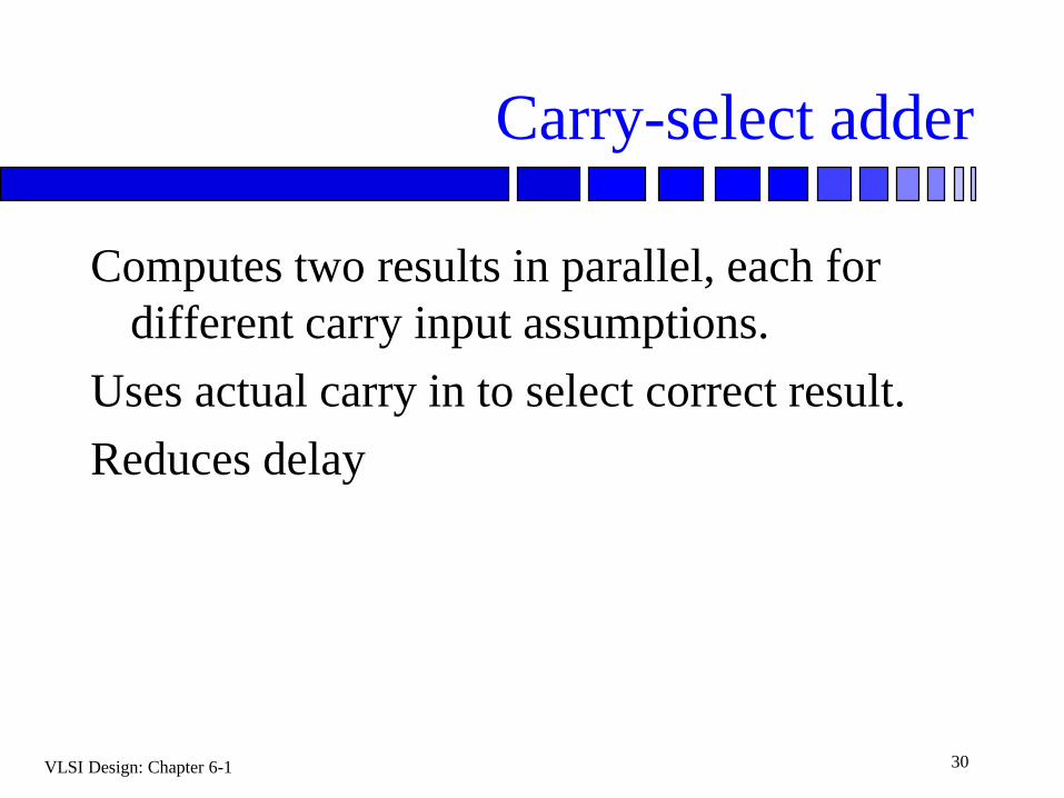
Carry-select adder
Computes two results in parallel, each for
different carry input assumptions.
Uses actual carry in to select correct result.
Reduces delay
VLSI Design: Chapter 6-1 31
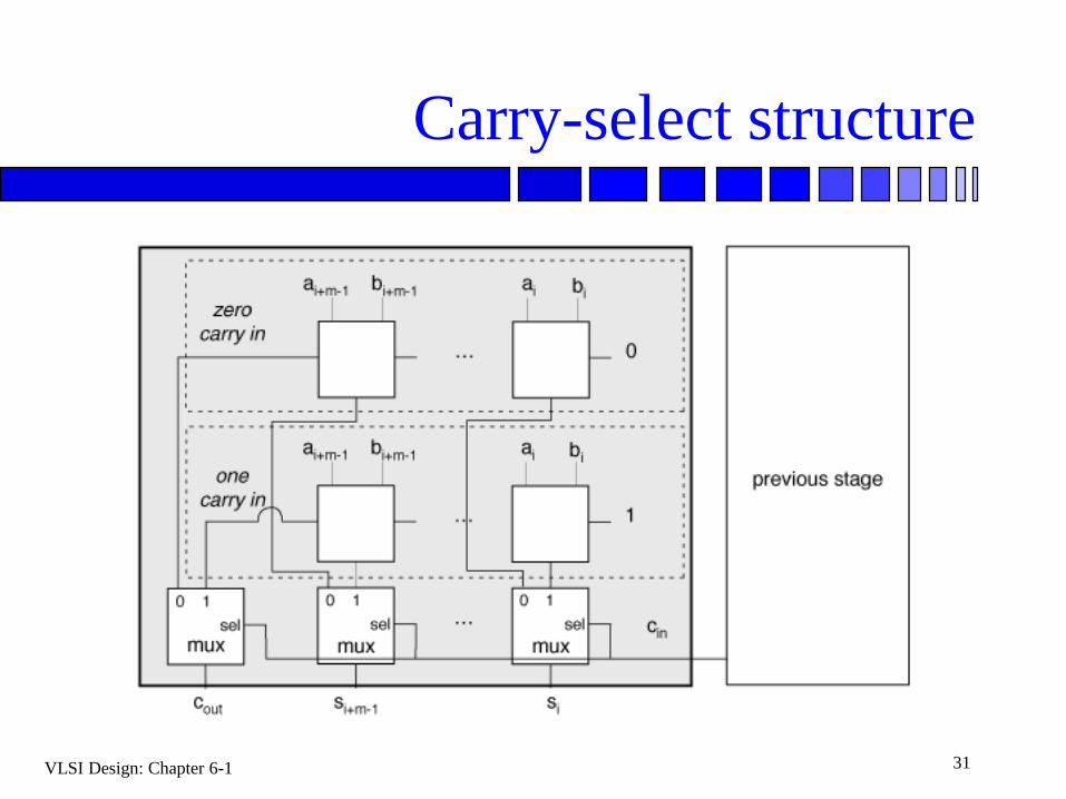
Carry-select structure
VLSI Design: Chapter 6-1 32
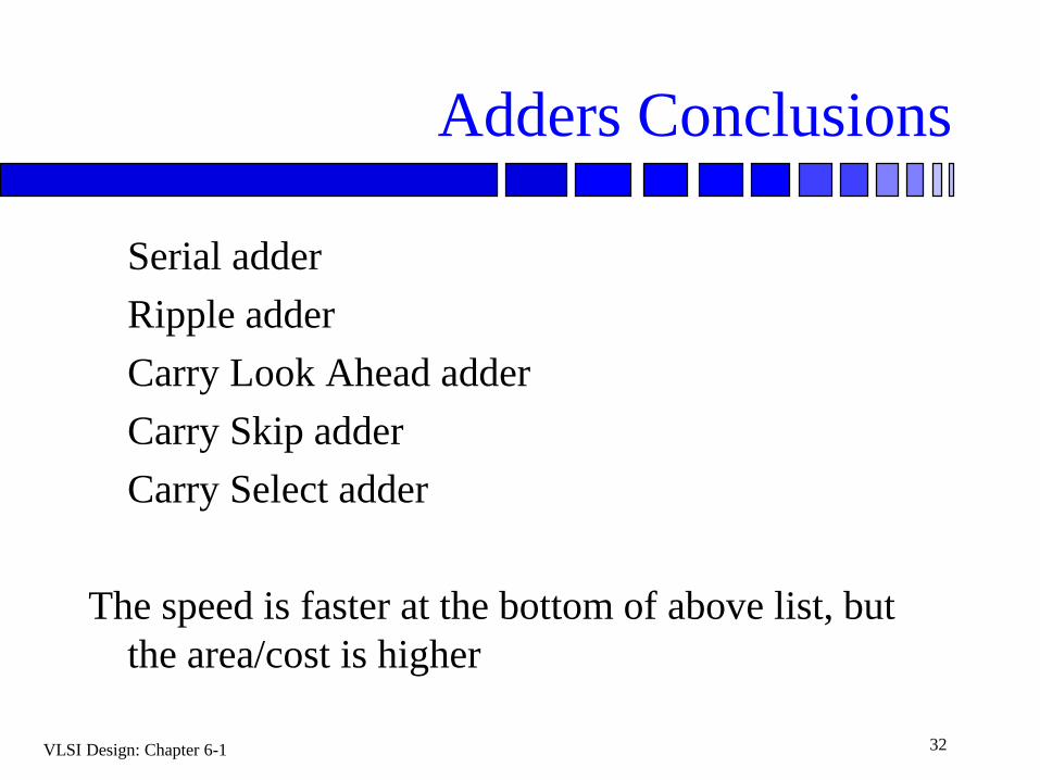
Adders Conclusions
Serial adder
Ripple adder
Carry Look Ahead adder
Carry Skip adder
Carry Select adder
The speed is faster at the bottom of above list, but
the area/cost is higher
VLSI Design: Chapter 6-1 33
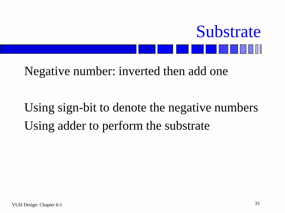
Substrate
Negative number: inverted then add one
Using sign-bit to denote the negative numbers
Using adder to perform the substrate
VLSI Design: Chapter 6-1 34
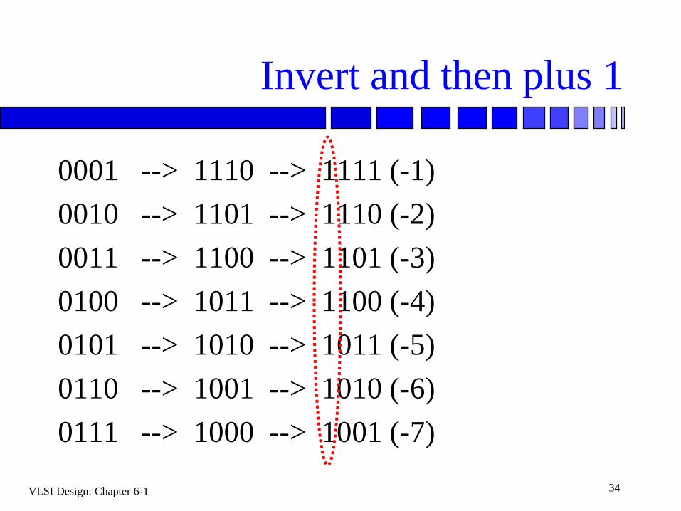
Invert and then plus 1
0001 --> 1110 --> 1111 (-1)
0010 --> 1101 --> 1110 (-2)
0011 --> 1100 --> 1101 (-3)
0100 --> 1011 --> 1100 (-4)
0101 --> 1010 --> 1011 (-5)
0110 --> 1001 --> 1010 (-6)
0111 --> 1000 --> 1001 (-7)
VLSI Design: Chapter 6-1 35
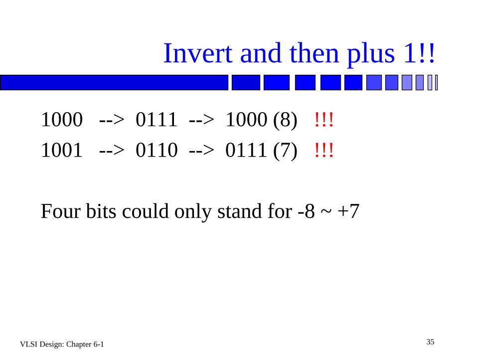
Invert and then plus 1!!
1000 --> 0111 --> 1000 (8) !!!
1001 --> 0110 --> 0111 (7) !!!
Four bits could only stand for -8 ~ +7
VLSI Design: Chapter 6-1 36
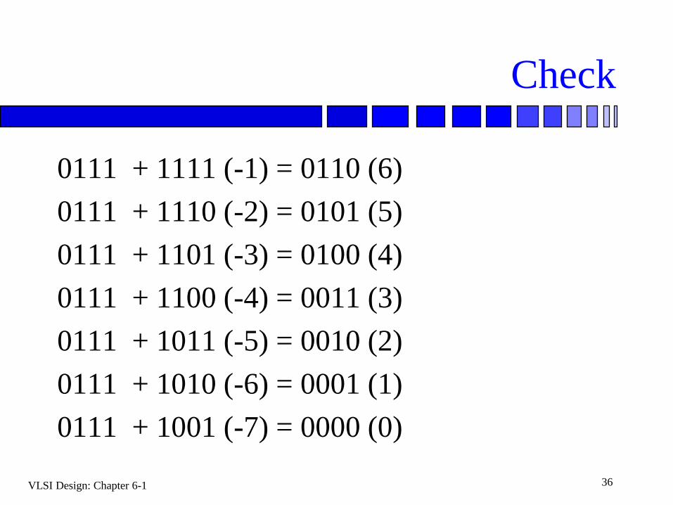
Check
0111 + 1111 (-1) = 0110 (6)
0111 + 1110 (-2) = 0101 (5)
0111 + 1101 (-3) = 0100 (4)
0111 + 1100 (-4) = 0011 (3)
0111 + 1011 (-5) = 0010 (2)
0111 + 1010 (-6) = 0001 (1)
0111 + 1001 (-7) = 0000 (0)
VLSI Design: Chapter 6-1 37
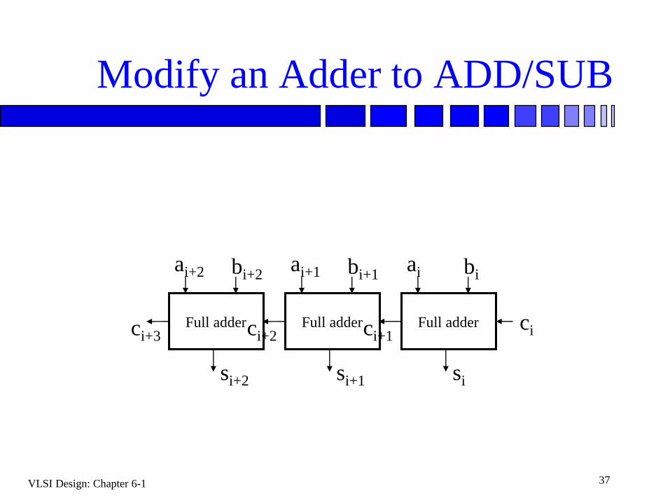
Modify an Adder to ADD/SUB
ai bi
ci
si
ci+1Full adder
ai+1
si+1
bi+1
ci+2Full adder
ai+2
si+2
bi+2
ci+3Full adder
VLSI Design: Chapter 6-1 38
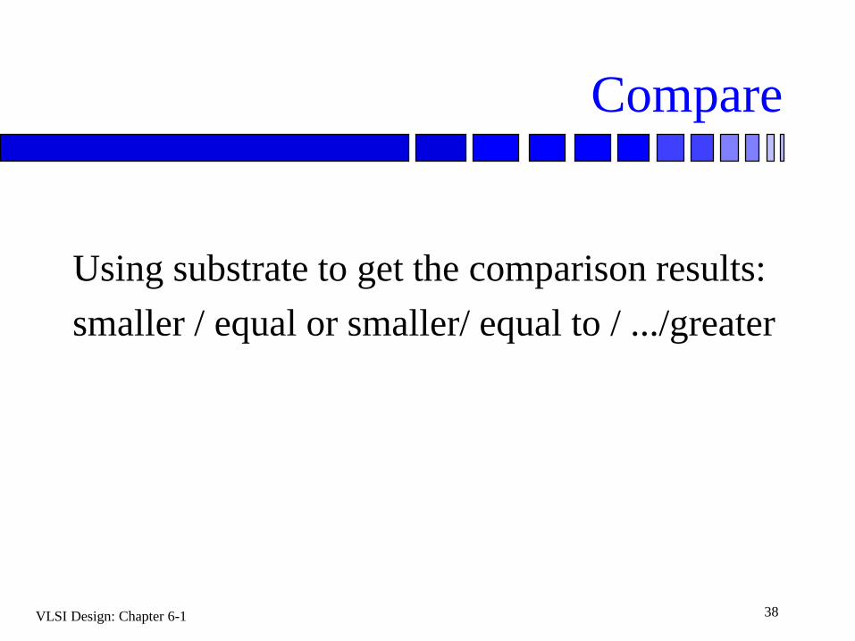
Compare
Using substrate to get the comparison results:
smaller / equal or smaller/ equal to / .../greater
VLSI Design: Chapter 6-1 39
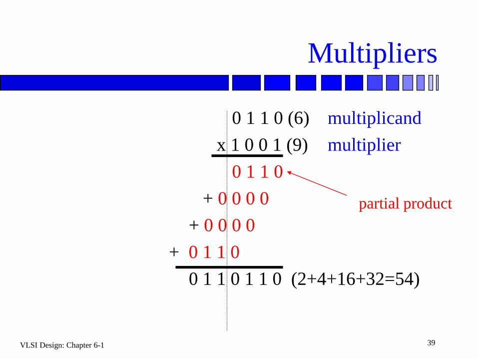
Multipliers
0 1 1 0 (6) multiplicand
x 1 0 0 1 (9) multiplier
0 1 1 0
+ 0 0 0 0
+ 0 0 0 0
+ 0 1 1 0
0 1 1 0 1 1 0 (2+4+16+32=54)
partial product
VLSI Design: Chapter 6-1 40
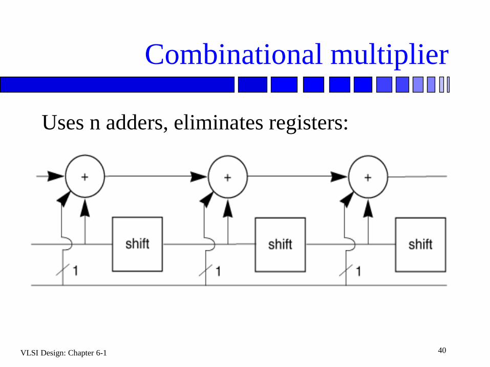
Combinational multiplier
Uses n adders, eliminates registers:
VLSI Design: Chapter 6-1 41
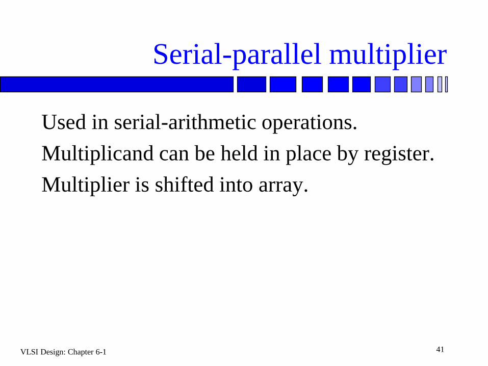
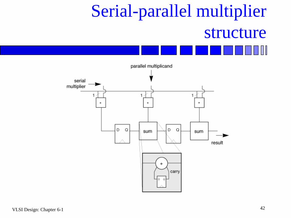
Serial-parallel multiplier
Used in serial-arithmetic operations.
Multiplicand can be held in place by register.
Multiplier is shifted into array.
VLSI Design: Chapter 6-1 42
Serial-parallel multiplier
structure
VLSI Design: Chapter 6-1 43
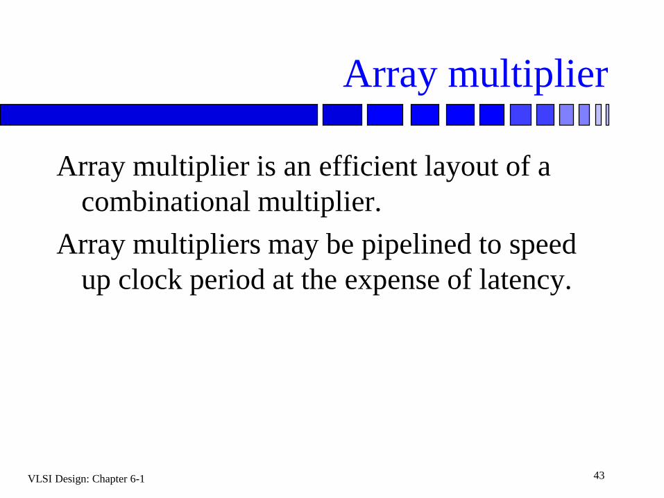
Array multiplier
Array multiplier is an efficient layout of a
combinational multiplier.
Array multipliers may be pipelined to speed
up clock period at the expense of latency.
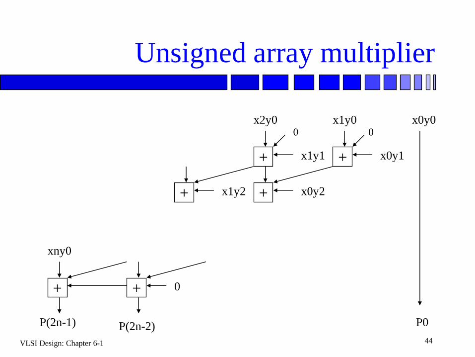
VLSI Design: Chapter 6-1 44
Unsigned array multiplier
+
x0y0x1y0x2y0
xny0
0
x0y1+ x1y1
0
+ x0y2+ x1y2
+ 0+
P(2n-1) P(2n-2) P0
VLSI Design: Chapter 6-1 45
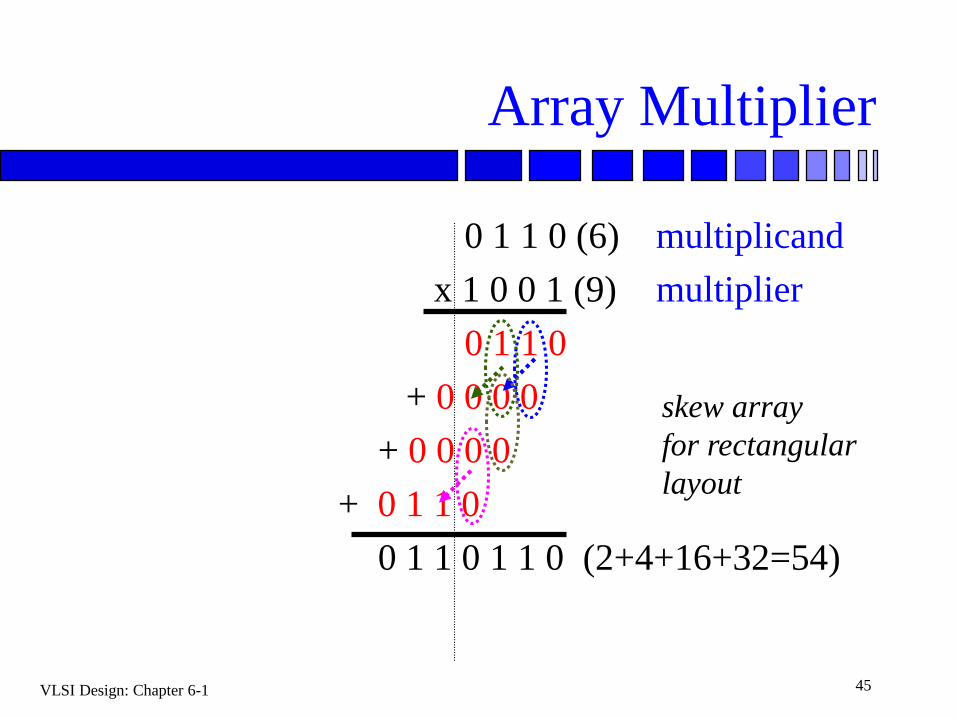
Array Multiplier
0 1 1 0 (6) multiplicand
x 1 0 0 1 (9) multiplier
0 1 1 0
+ 0 0 0 0
+ 0 0 0 0
+ 0 1 1 0
0 1 1 0 1 1 0 (2+4+16+32=54)
skew array
for rectangular
layout
VLSI Design: Chapter 6-1 46University of PatrasICECS 2010, Athens, Greece 46
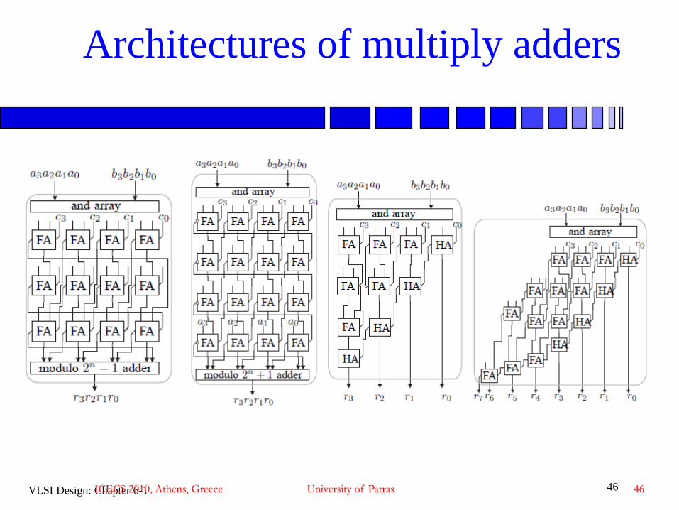
Architectures of multiply adders
VLSI Design: Chapter 6-1 47
Booth multiplier
Encoding scheme to reduce number of stages
in multiplication.
Performs two bits of multiplication at once—
requires half the stages.
Each stage is slightly more complex than
simple multiplier, but adder / subtracter is
almost as small/fast as adder.
VLSI Design: Chapter 6-1 48
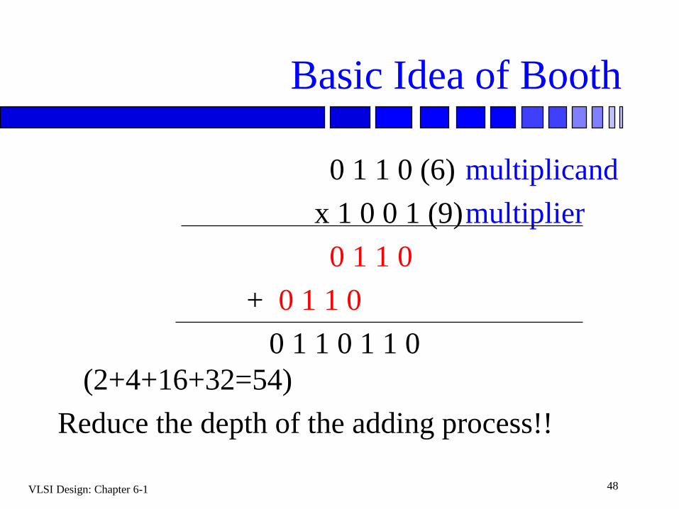
Basic Idea of Booth
0 1 1 0 (6) multiplicand
x 1 0 0 1 (9)multiplier
0 1 1 0
+ 0 1 1 0
0 1 1 0 1 1 0
(2+4+16+32=54)
Reduce the depth of the adding process!!
VLSI Design: Chapter 6-1 49
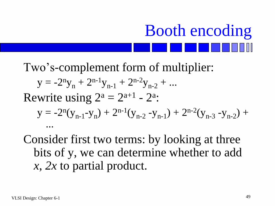
Booth encoding
Two’s-complement form of multiplier:
y = -2nyn + 2n-1yn-1 + 2n-2yn-2 + ...
Rewrite using 2a = 2a+1 - 2a:
y = -2n(yn-1-yn) + 2n-1(yn-2 -yn-1) + 2n-2(yn-3 -yn-2) + ...
Consider first two terms: by looking at three bits of y, we can determine whether to add x, 2x to partial product.
VLSI Design: Chapter 6-1 50
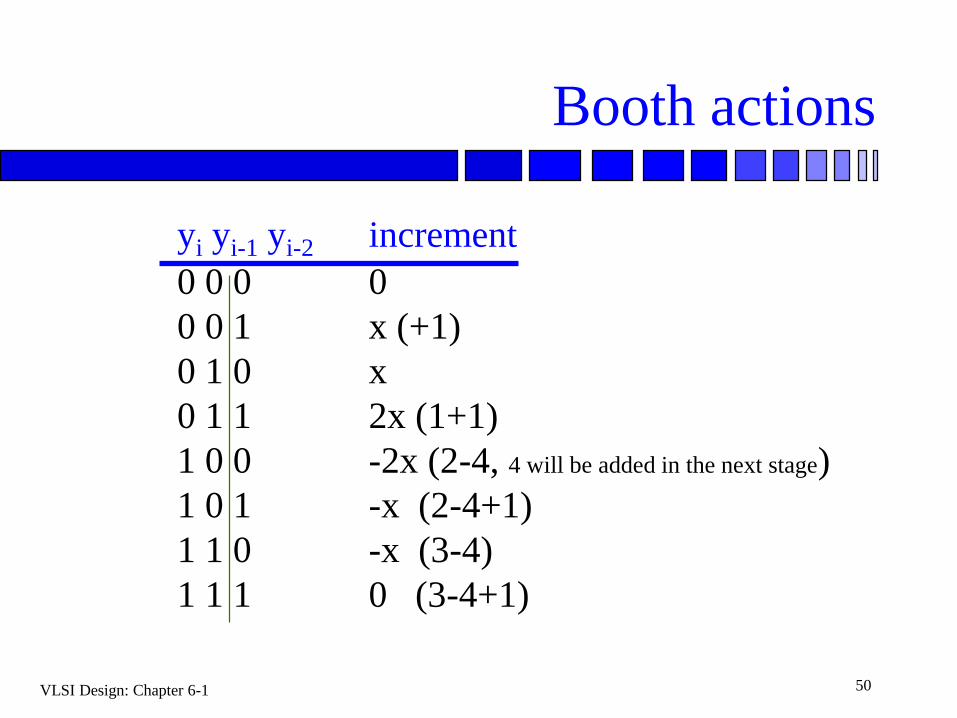
Booth actions
yi yi-1 yi-2 increment
0 0 0 0
0 0 1 x (+1)
0 1 0 x
0 1 1 2x (1+1)
1 0 0 -2x (2-4, 4 will be added in the next stage)
1 0 1 -x (2-4+1)
1 1 0 -x (3-4)
1 1 1 0 (3-4+1)
VLSI Design: Chapter 6-1 51
Booth actions(cont.)
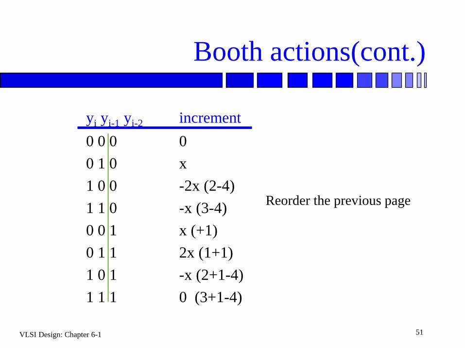
yi yi-1 yi-2 increment
0 0 0 0
0 1 0 x
1 0 0 -2x (2-4)
1 1 0 -x (3-4)
0 0 1 x (+1)
0 1 1 2x (1+1)
1 0 1 -x (2+1-4)
1 1 1 0 (3+1-4)
Reorder the previous page
VLSI Design: Chapter 6-1 52
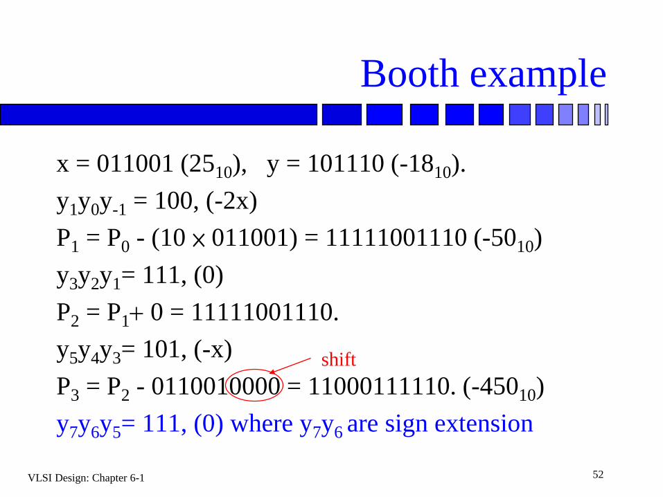
Booth example
x = 011001 (2510), y = 101110 (-1810).
y1y0y-1 = 100, (-2x)
P1 = P0 - (10 × 011001) = 11111001110 (-5010)
y3y2y1= 111, (0)
P2 = P1+ 0 = 11111001110.
y5y4y3= 101, (-x)
P3 = P2 - 0110010000 = 11000111110. (-45010)
y7y6y5= 111, (0) where y7y6 are sign extension
shift
VLSI Design: Chapter 6-1 53
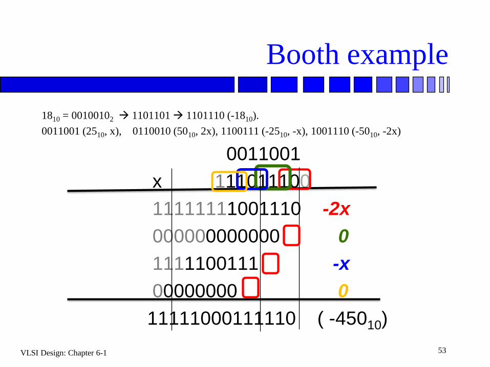
Booth example
1810 = 00100102 1101101 1101110 (-1810).
0011001 (2510, x), 0110010 (5010, 2x), 1100111 (-2510, -x), 1001110 (-5010, -2x)
0011001
x 111011100
11111111001110 -2x
000000000000 0
1111100111 -x
00000000 0
11111000111110 ( -45010)
VLSI Design: Chapter 6-1 54
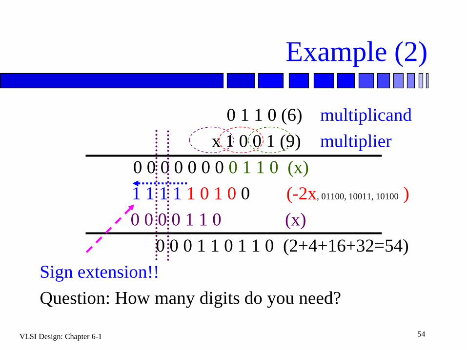
Example (2)
0 1 1 0 (6) multiplicand
x 1 0 0 1 (9) multiplier
0 0 0 0 0 0 0 0 1 1 0 (x)
1 1 1 1 1 0 1 0 0 (-2x, 01100, 10011, 10100 )
0 0 0 0 1 1 0 (x)
0 0 0 1 1 0 1 1 0 (2+4+16+32=54)
Sign extension!!
Question: How many digits do you need?
VLSI Design: Chapter 6-1 55
Example (2 cont.)
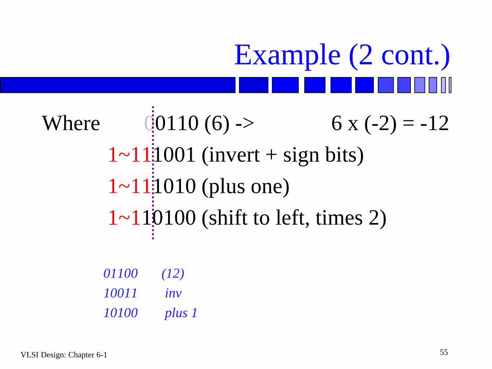
Where 00110 (6) -> 6 x (-2) = -12
1~111001 (invert + sign bits)
1~111010 (plus one)
1~110100 (shift to left, times 2)
01100 (12)
10011 inv
10100 plus 1
VLSI Design: Chapter 6-1 56
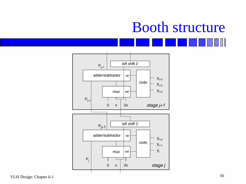
Booth structure
VLSI Design : Chapter 5-1 57
Schedule
11. 05/07/21 Chapter 6 (Multiplier)
12. 05/14/21 Chapter 7 (Placement, Routing, Special nets)
13. 05/21/21 Chapter 7 (Placement)
14. 05/28/21 Chapter 7 (Misc. before TO)
15. 06/04/21 (QZ2) Chapter 8 (Architecture)
16. 06/11/21 Chapter 8 (Architecture)
17. 06/18/21 Final Examination
18. 06/25/21 Exam review, What’s Next?
VLSI Design: Chapter 6-1 58
Wallace tree
Reduces depth of adder chain.
Built from full adders (carry save adders):
three inputs a, b, c
produces two outputs y, z such that
y + z = a + b + c
Carry-save equations:
yi = parity(ai,bi,ci)
zi = majority(ai,bi,ci)
VLSI Design: Chapter 6-1 59
Wallace tree operation
Final adder completes the summation.
Wiring is more complex.
Can build a Booth-encoded Wallace tree
multiplier.
VLSI Design: Chapter 6-1 60
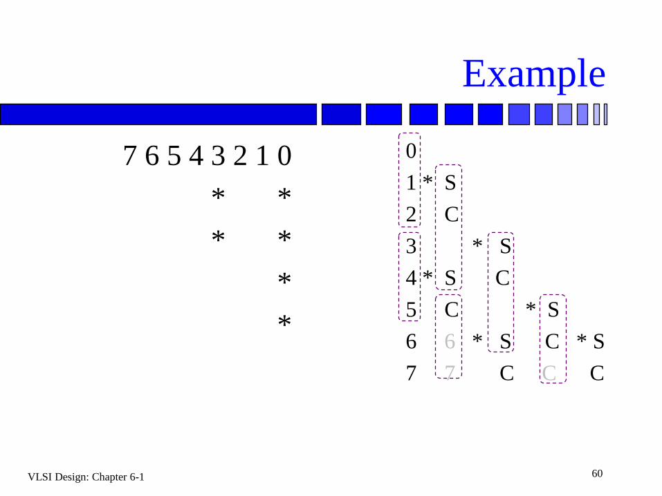
Example
7 6 5 4 3 2 1 0
* *
* *
*
*
0
1 * S
2 C
3 * S
4 * S C
5 C * S
6 6 * S C * S
7 7 C C C
VLSI Design: Chapter 6-1 61
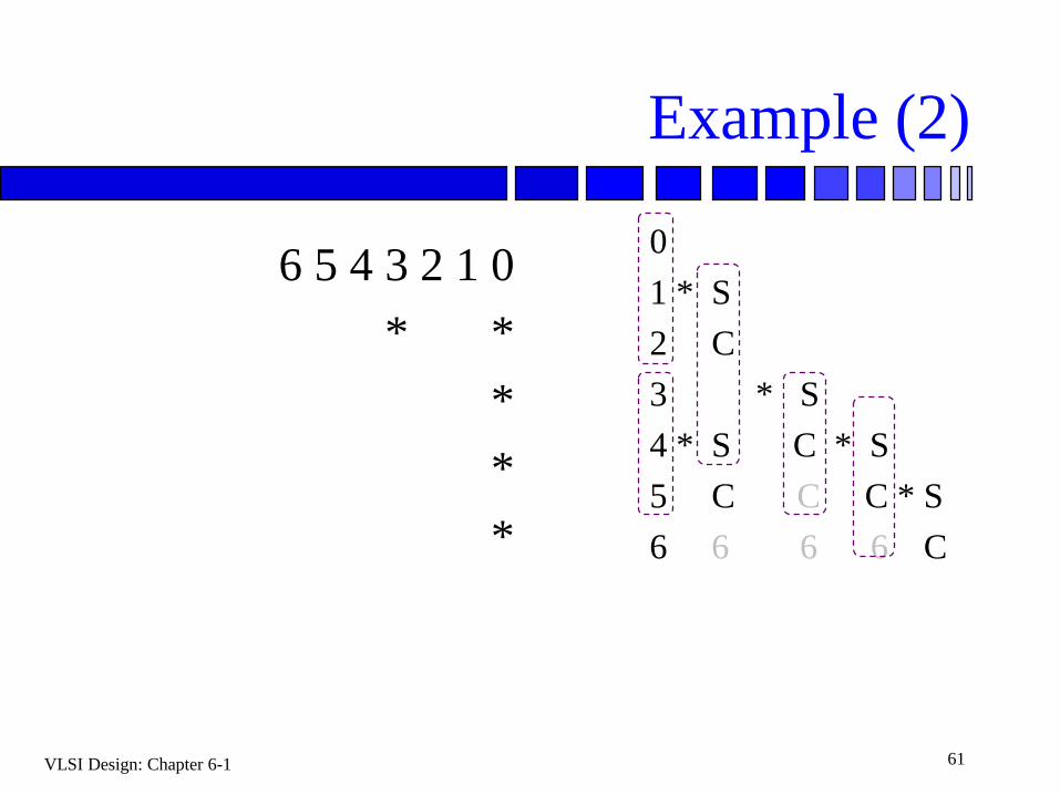
Example (2)
6 5 4 3 2 1 0
* *
*
*
*
0
1 * S
2 C
3 * S
4 * S C * S
5 C C C * S
6 6 6 6 C
VLSI Design: Chapter 6-1 62
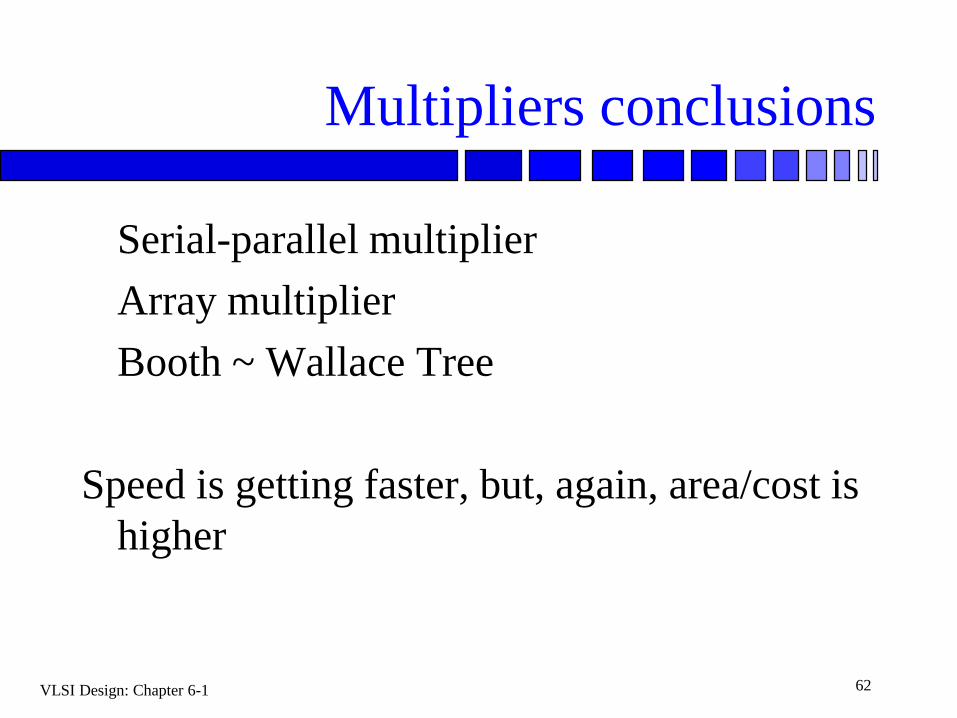
Multipliers conclusions
Serial-parallel multiplier
Array multiplier
Booth ~ Wallace Tree
Speed is getting faster, but, again, area/cost is
higher
VLSI Design: Chapter 6-1 63
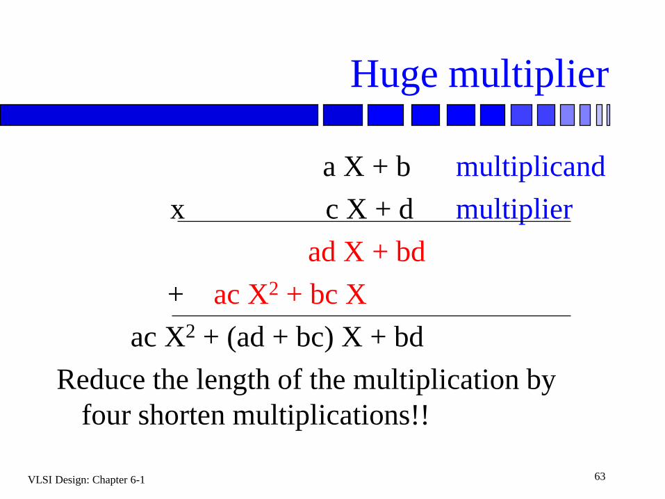
Huge multiplier
a X + b multiplicand
x c X + d multiplier
ad X + bd
+ ac X2 + bc X
ac X2 + (ad + bc) X + bd
Reduce the length of the multiplication by
four shorten multiplications!!
VLSI Design: Chapter 6-1 64
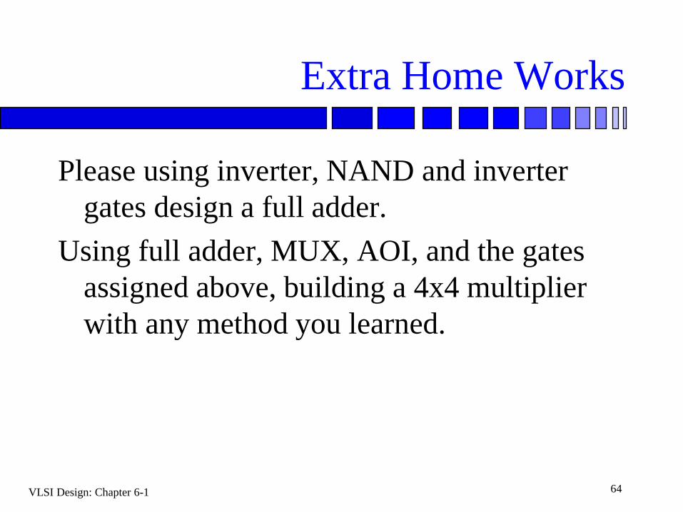
Extra Home Works
Please using inverter, NAND and inverter
gates design a full adder.
Using full adder, MUX, AOI, and the gates
assigned above, building a 4x4 multiplier
with any method you learned.
VLSI Design: Chapter 6-1 65
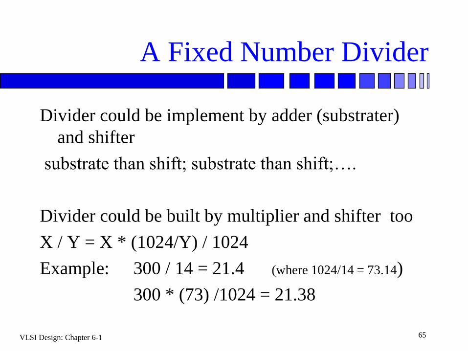
A Fixed Number Divider
Divider could be implement by adder (substrater)
and shifter
substrate than shift; substrate than shift;….
Divider could be built by multiplier and shifter too
X / Y = X * (1024/Y) / 1024
Example: 300 / 14 = 21.4 (where 1024/14 = 73.14)
300 * (73) /1024 = 21.38
VLSI Design: Chapter 6-1 66
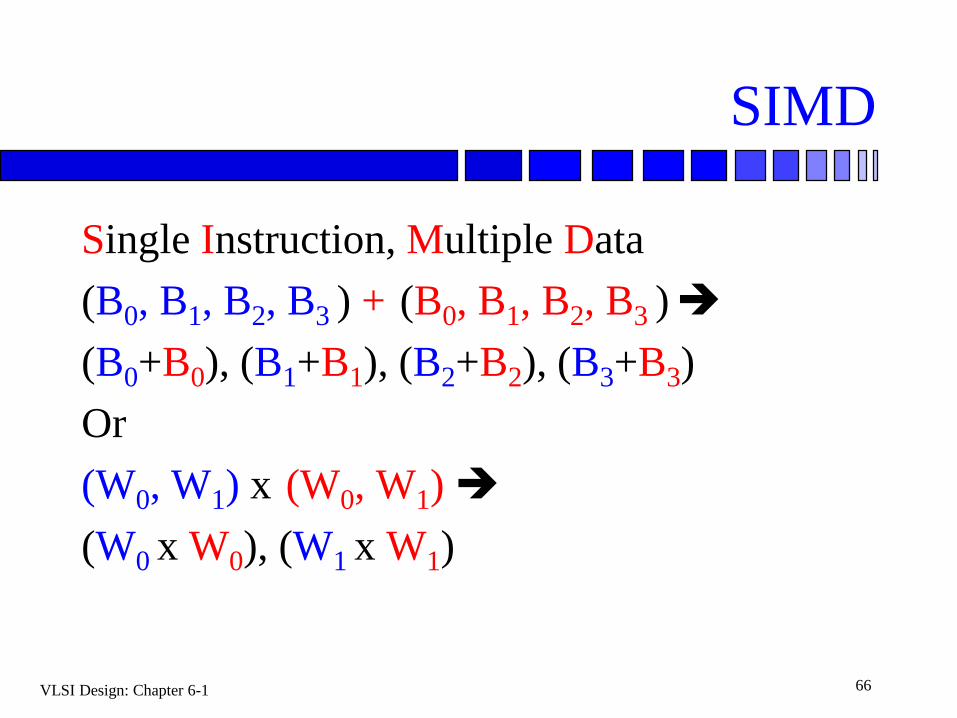
SIMD
Single Instruction, Multiple Data
(B0, B1, B2, B3 ) + (B0, B1, B2, B3 )
(B0+B0), (B1+B1), (B2+B2), (B3+B3)
Or
(W0, W1) x (W0, W1)
(W0 x W0), (W1 x W1)
VLSI Design: Chapter 6-1 67
SIMD
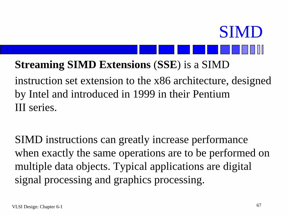
Streaming SIMD Extensions (SSE) is a SIMD
instruction set extension to the x86 architecture, designed
by Intel and introduced in 1999 in their Pentium
III series.
SIMD instructions can greatly increase performance
when exactly the same operations are to be performed on
multiple data objects. Typical applications are digital
signal processing and graphics processing.
VLSI Design: Chapter 6-1 68
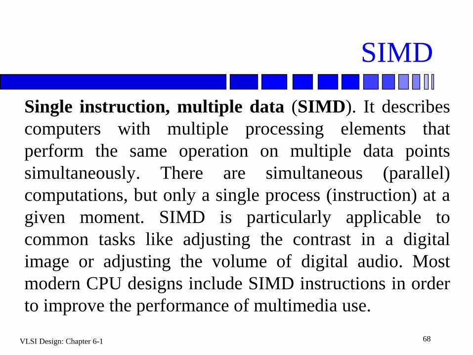
SIMD
Single instruction, multiple data (SIMD). It describes
computers with multiple processing elements that
perform the same operation on multiple data points
simultaneously. There are simultaneous (parallel)
computations, but only a single process (instruction) at a
given moment. SIMD is particularly applicable to
common tasks like adjusting the contrast in a digital
image or adjusting the volume of digital audio. Most
modern CPU designs include SIMD instructions in order
to improve the performance of multimedia use.
VLSI Design: Chapter 6-1 69
GPU / VPU
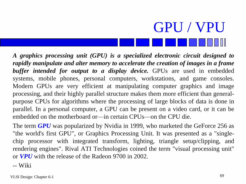
A graphics processing unit (GPU) is a specialized electronic circuit designed to
rapidly manipulate and alter memory to accelerate the creation of images in a frame
buffer intended for output to a display device. GPUs are used in embedded
systems, mobile phones, personal computers, workstations, and game consoles.
Modern GPUs are very efficient at manipulating computer graphics and image
processing, and their highly parallel structure makes them more efficient than general-
purpose CPUs for algorithms where the processing of large blocks of data is done in
parallel. In a personal computer, a GPU can be present on a video card, or it can be
embedded on the motherboard or—in certain CPUs—on the CPU die.
The term GPU was popularized by Nvidia in 1999, who marketed the GeForce 256 as
"the world's first GPU", or Graphics Processing Unit. It was presented as a "single-
chip processor with integrated transform, lighting, triangle setup/clipping, and
rendering engines". Rival ATI Technologies coined the term "visual processing unit"
or VPU with the release of the Radeon 9700 in 2002.
-- Wiki
VLSI Design: Chapter 6-1 70
AI processor / GPGPU / TPU
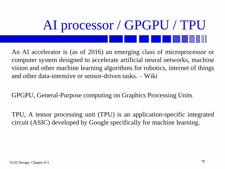
An AI accelerator is (as of 2016) an emerging class of microprocessor or
computer system designed to accelerate artificial neural networks, machine
vision and other machine learning algorithms for robotics, internet of things
and other data-intensive or sensor-driven tasks. – Wiki
GPGPU, General-Purpose computing on Graphics Processing Units
TPU, A tensor processing unit (TPU) is an application-specific integrated
circuit (ASIC) developed by Google specifically for machine learning.
VLSI Design: Chapter 6-1 71
Chapter 6: System Design
Datapath.
PLAs.
VLSI Design: Chapter 6-1 72
Data paths
A data path is a logical and a physical
structure:
bitwise logical organization;
bitwise physical design.
Datapath often has ALU, registers, some other
function units.
Data is passed via busses.
VLSI Design: Chapter 6-1 73
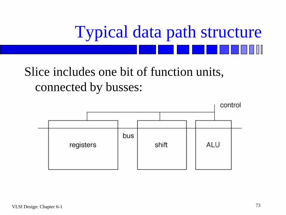
Typical data path structure
Slice includes one bit of function units,
connected by busses:
VLSI Design: Chapter 6-1 74
Bit-slice structure
Many arithmetic and logical functions can be
defined recursively on bits of word.
A bit-slice is one-bit (or n-bit) segment of an
operation of minimum size to ensure
regularity.
Regular logical structure allows regular
physical structure.
VLSI Design: Chapter 6-1 75
Abutting and pitch-matching
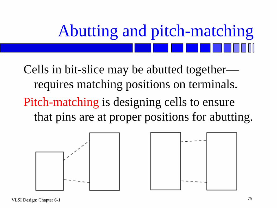
Cells in bit-slice may be abutted together—
requires matching positions on terminals.
Pitch-matching is designing cells to ensure
that pins are at proper positions for abutting.
VLSI Design: Chapter 6-1 76
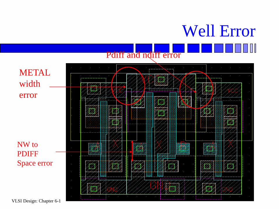
Well Error
NW to
PDIFF
Space error
METAL
width
error
Pdiff and ndiff error
VLSI Design: Chapter 6-1 77
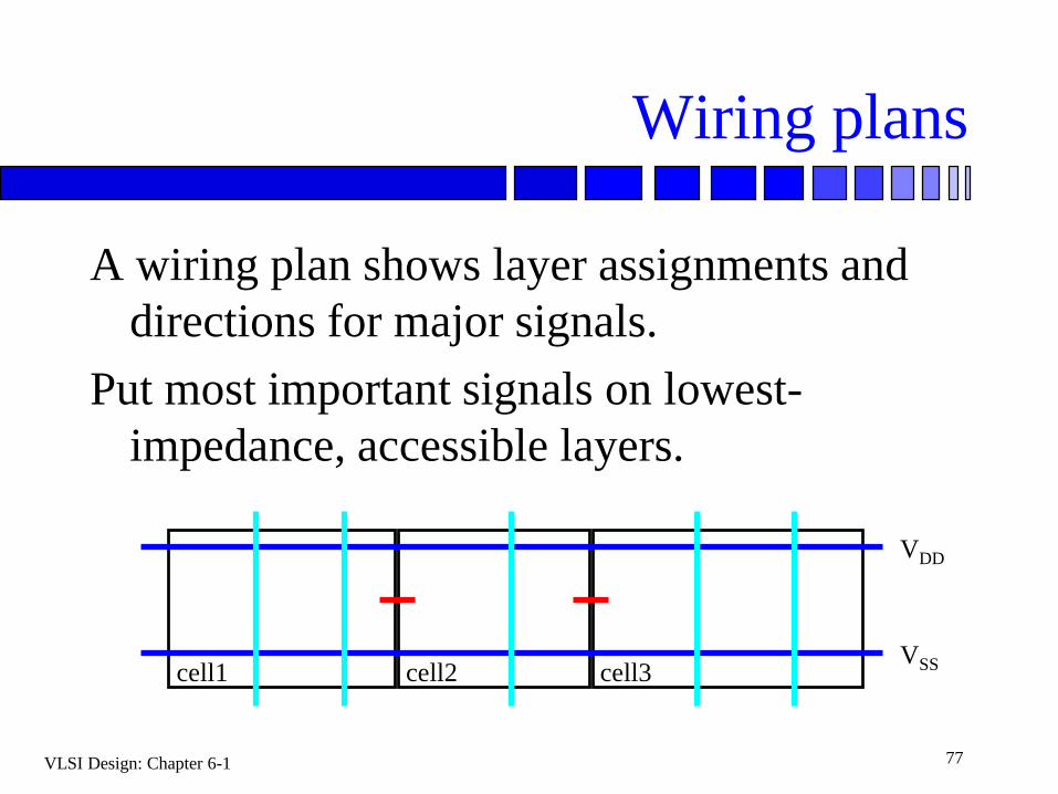
Wiring plans
A wiring plan shows layer assignments and
directions for major signals.
Put most important signals on lowest-
impedance, accessible layers.
cell1 cell2 cell3
VDD
VSS
VLSI Design: Chapter 6-1 78
Example
Pick a process ( 1P3M, 2P5M…).
Decide cell height (MUX821 or DFF with rstn).
Calculate how many routing channels can be
use in the X direction.
Make a rough floorplan for datapath and
calculate the wires go through any Y-
direction cross-section.
VLSI Design: Chapter 6-1 79
Programmable logic array (PLA)
Used to implement special logic functions.
A PLA decodes only some addresses (input
values); a ROM decodes all addresses.
PLA not as common in CMOS as in nMOS,
but it has been used for logic functions.
VLSI Design: Chapter 6-1 80
PLA continue
Any pure logic function can be build with
only AND, OR, INV functions and
expressed as a truth table.
We implement the truth table into a
Programmable Logic Array (PLA).
VLSI Design: Chapter 6-1 81
Homework (2)
Chapter 6: 6-8 (a), (b), and (c)