Embed Size (px)
Citation preview
±0.5°C Accurate, 16-Bit Digital I2C Temperature Sensor
Data Sheet ADT7410
Rev. C Document Feedback Information furnished by Analog Devices is believed to be accurate and reliable. However, no responsibility is assumed by Analog Devices for its use, nor for any infringements of patents or other rights of third parties that may result from its use. Specifications subject to change without notice. No license is granted by implication or otherwise under any patent or patent rights of Analog Devices. Trademarks and registered trademarks are the property of their respective owners.
One Technology Way, P.O. Box 9106, Norwood, MA 02062-9106, U.S.A. Tel: 781.329.4700 ©2009–2017 Analog Devices, Inc. All rights reserved. Technical Support www.analog.com
FEATURES High performance
Temperature accuracy ±0.5°C from −40°C to +105°C (2.7 V to 3.6 V) ±0.4°C from −40°C to +105°C (3.0 V)
16-bit temperature resolution: 0.0078°C Fast first temperature conversion on power-up of 6 ms
Easy implementation No temperature calibration/correction required by user No linearity correction required
Low power Power saving 1 sample per second (SPS) mode 700 µW typical at 3.3 V in normal mode 7 µW typical at 3.3 V in shutdown mode
Wide operating ranges Temperature range: −55°C to +150°C Voltage range: 2.7 V to 5.5 V
Programmable interrupts Critical overtemperature interrupt Overtemperature/undertemperature interrupt
I2C-compatible interface 8-lead narrow SOIC RoHS-compliant package
APPLICATIONS Medical equipment Environmental control systems Computer thermal monitoring Thermal protection Industrial process control Power system monitors Hand-held applications
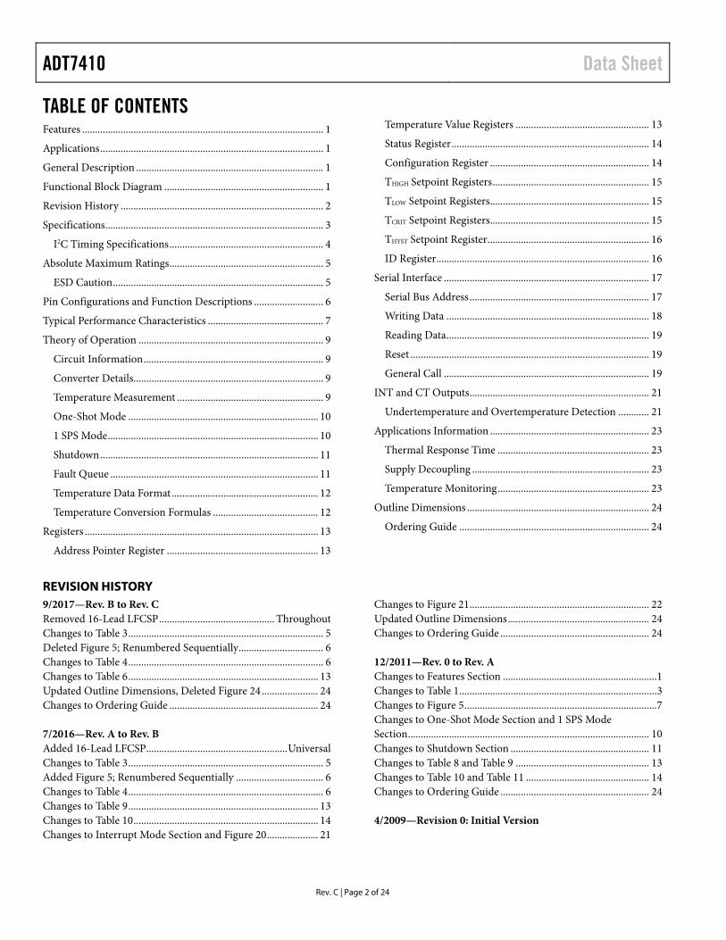
GENERAL DESCRIPTION The ADT7410 is a high accuracy digital temperature sensor in a narrow SOIC package. It contains a band gap temperature reference and a 13-bit ADC to monitor and digitize the temperature to a 0.0625°C resolution. The ADC resolution, by default, is set to 13 bits (0.0625°C). This can be changed to 16 bits (0.0078°C) by setting Bit 7 in the configuration register (Register Address 0x03).
The ADT7410 is guaranteed to operate over supply voltages from 2.7 V to 5.5 V. Operating at 3.3 V, the average supply current is typi-cally 210 μA. The ADT7410 has a shutdown mode that powers down the device and offers a shutdown current of typically 2 μA. The ADT7410 is rated for operation over the −55°C to +150°C temperature range.
Pin A0 and Pin A1 are available for address selection, giving the ADT7410 four possible I2C addresses. The CT pin is an open-drain output that becomes active when the temperature exceeds a programmable critical temperature limit. The default critical temperature limit is 147°C. The INT pin is also an open-drain output that becomes active when the temperature exceeds a programmable limit. The INT and CT pins can operate in either comparator or interrupt mode.
FUNCTIONAL BLOCK DIAGRAM
TEMPERATUREVALUE
REGISTER
CONFIGURATIONREGISTER
THYSTREGISTER
TLOWREGISTER
THIGHREGISTER
TCRITREGISTER
POINTERREGISTER
INTERNALREFERENCE
8
7
TEMPERATURESENSOR
THIGH
TCRIT
TLOW
INTERNALOSCILLATOR
FILTERLOGIC
Σ-ΔMODULATOR
VDD
GND
6
5
CT
INT
3
4
A0A1
1
2
SCLSDA
I2C INTERFACE
ADT7410
0656
0-00
1
Figure 1.
ADT7410 Data Sheet
Rev. C | Page 2 of 24
TABLE OF CONTENTS Features .............................................................................................. 1 Applications ....................................................................................... 1 General Description ......................................................................... 1 Functional Block Diagram .............................................................. 1 Revision History ............................................................................... 2 Specifications ..................................................................................... 3
I2C Timing Specifications ............................................................ 4 Absolute Maximum Ratings ............................................................ 5
ESD Caution .................................................................................. 5 Pin Configurations and Function Descriptions ........................... 6 Typical Performance Characteristics ............................................. 7 Theory of Operation ........................................................................ 9
Circuit Information ...................................................................... 9 Converter Details .......................................................................... 9 Temperature Measurement ......................................................... 9 One-Shot Mode .......................................................................... 10 1 SPS Mode .................................................................................. 10 Shutdown ..................................................................................... 11 Fault Queue ................................................................................. 11 Temperature Data Format ......................................................... 12 Temperature Conversion Formulas ......................................... 12
Registers ........................................................................................... 13
Address Pointer Register ........................................................... 13
Temperature Value Registers .................................................... 13 Status Register ............................................................................. 14 Configuration Register .............................................................. 14 THIGH Setpoint Registers ............................................................. 15 TLOW Setpoint Registers .............................................................. 15 TCRIT Setpoint Registers .............................................................. 15 THYST Setpoint Register ............................................................... 16 ID Register................................................................................... 16
Serial Interface ................................................................................ 17 Serial Bus Address ...................................................................... 17 Writing Data ............................................................................... 18 Reading Data ............................................................................... 19 Reset ............................................................................................. 19 General Call ................................................................................ 19
INT and CT Outputs ...................................................................... 21 Undertemperature and Overtemperature Detection ............ 21
Applications Information .............................................................. 23 Thermal Response Time ........................................................... 23 Supply Decoupling ..................................................................... 23 Temperature Monitoring ........................................................... 23
Outline Dimensions ....................................................................... 24 Ordering Guide .......................................................................... 24
REVISION HISTORY 9/2017—Rev. B to Rev. C Removed 16-Lead LFCSP ............................................. Throughout Changes to Table 3 ............................................................................ 5 Deleted Figure 5; Renumbered Sequentially ................................. 6 Changes to Table 4 ............................................................................ 6 Changes to Table 6 .......................................................................... 13 Updated Outline Dimensions, Deleted Figure 24 ...................... 24 Changes to Ordering Guide .......................................................... 24 7/2016—Rev. A to Rev. B Added 16-Lead LFCSP ....................................................... Universal Changes to Table 3 ............................................................................ 5 Added Figure 5; Renumbered Sequentially .................................. 6 Changes to Table 4 ............................................................................ 6 Changes to Table 9 .......................................................................... 13 Changes to Table 10 ........................................................................ 14 Changes to Interrupt Mode Section and Figure 20 .................... 21
Changes to Figure 21 ...................................................................... 22 Updated Outline Dimensions ....................................................... 24 Changes to Ordering Guide .......................................................... 24 12/2011—Rev. 0 to Rev. A Changes to Features Section ............................................................ 1 Changes to Table 1 ............................................................................. 3 Changes to Figure 5 ........................................................................... 7 Changes to One-Shot Mode Section and 1 SPS Mode Section .............................................................................................. 10 Changes to Shutdown Section ...................................................... 11 Changes to Table 8 and Table 9 .................................................... 13 Changes to Table 10 and Table 11 ................................................ 14 Changes to Ordering Guide .......................................................... 24 4/2009—Revision 0: Initial Version
Data Sheet ADT7410
Rev. C | Page 3 of 24
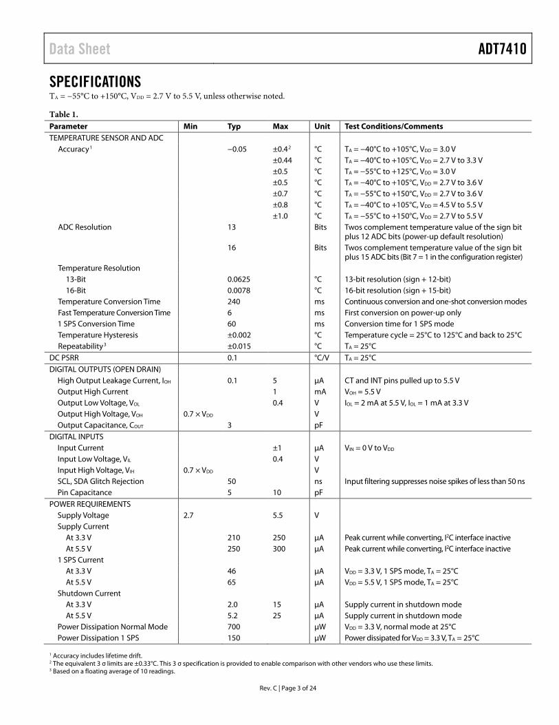
SPECIFICATIONS TA = −55°C to +150°C, VDD = 2.7 V to 5.5 V, unless otherwise noted.
Table 1. Parameter Min Typ Max Unit Test Conditions/Comments TEMPERATURE SENSOR AND ADC
Accuracy1 −0.05 ±0.42 °C TA = −40°C to +105°C, VDD = 3.0 V ±0.44 °C TA = −40°C to +105°C, VDD = 2.7 V to 3.3 V ±0.5 °C TA = −55°C to +125°C, VDD = 3.0 V ±0.5 °C TA = −40°C to +105°C, VDD = 2.7 V to 3.6 V ±0.7 °C TA = −55°C to +150°C, VDD = 2.7 V to 3.6 V ±0.8 °C TA = −40°C to +105°C, VDD = 4.5 V to 5.5 V ±1.0 °C TA = −55°C to +150°C, VDD = 2.7 V to 5.5 V ADC Resolution 13 Bits Twos complement temperature value of the sign bit
plus 12 ADC bits (power-up default resolution) 16 Bits Twos complement temperature value of the sign bit
plus 15 ADC bits (Bit 7 = 1 in the configuration register) Temperature Resolution
13-Bit 0.0625 °C 13-bit resolution (sign + 12-bit) 16-Bit 0.0078 °C 16-bit resolution (sign + 15-bit)
Temperature Conversion Time 240 ms Continuous conversion and one-shot conversion modes Fast Temperature Conversion Time 6 ms First conversion on power-up only 1 SPS Conversion Time 60 ms Conversion time for 1 SPS mode Temperature Hysteresis ±0.002 °C Temperature cycle = 25°C to 125°C and back to 25°C Repeatability3 ±0.015 °C TA = 25°C
DC PSRR 0.1 °C/V TA = 25°C DIGITAL OUTPUTS (OPEN DRAIN)
High Output Leakage Current, IOH 0.1 5 µA CT and INT pins pulled up to 5.5 V Output High Current 1 mA VOH = 5.5 V Output Low Voltage, VOL 0.4 V IOL = 2 mA at 5.5 V, IOL = 1 mA at 3.3 V Output High Voltage, VOH 0.7 × VDD V Output Capacitance, COUT 3 pF
DIGITAL INPUTS Input Current ±1 µA VIN = 0 V to VDD Input Low Voltage, VIL 0.4 V Input High Voltage, VIH 0.7 × VDD V SCL, SDA Glitch Rejection 50 ns Input filtering suppresses noise spikes of less than 50 ns Pin Capacitance 5 10 pF
POWER REQUIREMENTS Supply Voltage 2.7 5.5 V Supply Current
At 3.3 V 210 250 µA Peak current while converting, I2C interface inactive At 5.5 V 250 300 µA Peak current while converting, I2C interface inactive
1 SPS Current At 3.3 V 46 µA VDD = 3.3 V, 1 SPS mode, TA = 25°C At 5.5 V 65 µA VDD = 5.5 V, 1 SPS mode, TA = 25°C
Shutdown Current At 3.3 V 2.0 15 µA Supply current in shutdown mode At 5.5 V 5.2 25 µA Supply current in shutdown mode
Power Dissipation Normal Mode 700 µW VDD = 3.3 V, normal mode at 25°C Power Dissipation 1 SPS 150 µW Power dissipated for VDD = 3.3 V, TA = 25°C
1 Accuracy includes lifetime drift. 2 The equivalent 3 σ limits are ±0.33°C. This 3 σ specification is provided to enable comparison with other vendors who use these limits. 3 Based on a floating average of 10 readings.
ADT7410 Data Sheet
Rev. C | Page 4 of 24
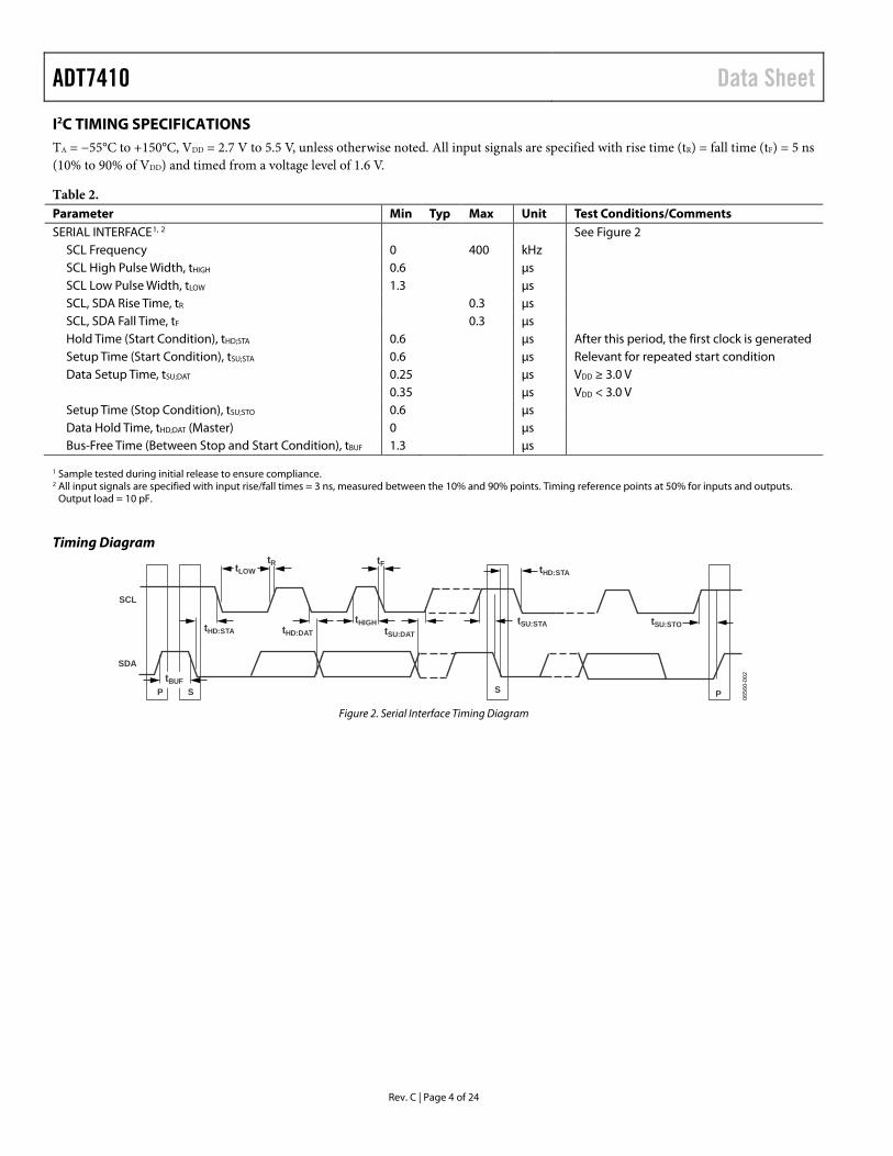
I2C TIMING SPECIFICATIONS TA = −55°C to +150°C, VDD = 2.7 V to 5.5 V, unless otherwise noted. All input signals are specified with rise time (tR) = fall time (tF) = 5 ns (10% to 90% of VDD) and timed from a voltage level of 1.6 V.
Table 2. Parameter Min Typ Max Unit Test Conditions/Comments SERIAL INTERFACE1, 2 See Figure 2
SCL Frequency 0 400 kHz SCL High Pulse Width, tHIGH 0.6 µs SCL Low Pulse Width, tLOW 1.3 µs SCL, SDA Rise Time, tR 0.3 µs SCL, SDA Fall Time, tF 0.3 µs Hold Time (Start Condition), tHD;STA 0.6 µs After this period, the first clock is generated Setup Time (Start Condition), tSU;STA 0.6 µs Relevant for repeated start condition Data Setup Time, tSU;DAT 0.25 µs VDD ≥ 3.0 V 0.35 µs VDD < 3.0 V Setup Time (Stop Condition), tSU;STO 0.6 µs Data Hold Time, tHD;DAT (Master) 0 µs Bus-Free Time (Between Stop and Start Condition), tBUF 1.3 µs
1 Sample tested during initial release to ensure compliance. 2 All input signals are specified with input rise/fall times = 3 ns, measured between the 10% and 90% points. Timing reference points at 50% for inputs and outputs.
Output load = 10 pF.
Timing Diagram
0656
0-00
2
PS
tLOWtR tF
tHD:STA tHD:DAT tSU:DATtSU:STA
tHD:STA
tSU:STOtHIGH
SCL
P S
SDAtBUF
Figure 2. Serial Interface Timing Diagram
Data Sheet ADT7410
Rev. C | Page 5 of 24
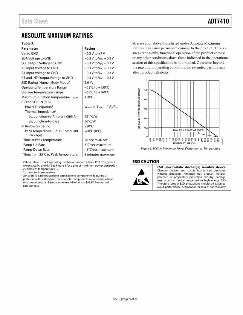
ABSOLUTE MAXIMUM RATINGS Table 3. Parameter Rating VDD to GND −0.3 V to +7 V SDA Voltage to GND −0.3 V to VDD + 0.3 V SCL Output Voltage to GND −0.3 V to VDD + 0.3 V A0 Input Voltage to GND −0.3 V to VDD + 0.3 V A1 Input Voltage to GND −0.3 V to VDD + 0.3 V CT and INT Output Voltage to GND −0.3 V to VDD + 0.3 V ESD Rating (Human Body Model) 2.0 kV Operating Temperature Range −55°C to +150°C Storage Temperature Range −65°C to +160°C Maximum Junction Temperature, TJMAX 150°C 8-Lead SOIC-N (R-8)
Power Dissipation1 WMAX = (TJMAX − TA2)/θJA
Thermal Impedance3 θJA, Junction-to-Ambient (Still Air) 121°C/W θJC, Junction-to-Case 56°C/W
IR Reflow Soldering 220°C Peak Temperature (RoHS-Compliant
Package) 260°C (0°C)
Time at Peak Temperature 20 sec to 40 sec Ramp-Up Rate 3°C/sec maximum Ramp-Down Rate −6°C/sec maximum Time from 25°C to Peak Temperature 8 minutes maximum
1 Values relate to package being used on a standard 2-layer PCB. This gives a
worst-case θJA and θJC. See Figure 3 for a plot of maximum power dissipation vs. ambient temperature (TA).
2 TA = ambient temperature. 3 Junction-to-case resistance is applicable to components featuring a
preferential flow direction, for example, components mounted on a heat sink. Junction-to-ambient is more useful for air-cooled, PCB-mounted components.
Stresses at or above those listed under Absolute Maximum Ratings may cause permanent damage to the product. This is a stress rating only; functional operation of the product at these or any other conditions above those indicated in the operational section of this specification is not implied. Operation beyond the maximum operating conditions for extended periods may affect product reliability.
0656
0-00
3
TEMPERATURE (°C)
MA
XIM
UM
PO
WER
DIS
SIPA
TIO
N (W
)
1.2
0.8
1.0
0.6
0.2
0.4
0
–55
–50
–40
–30
–20
–10 0 10 20 30 40 50 60 70 80 90 100
110
120
130
140
150
MAX PD = 3.4mW AT 150°C
Figure 3. SOIC_N Maximum Power Dissipation vs. Temperature
ESD CAUTION
ADT7410 Data Sheet
Rev. C | Page 6 of 24
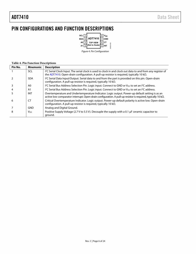
PIN CONFIGURATIONS AND FUNCTION DESCRIPTIONS SCL 1
SDA 2
A0 3
A1 4
VDD8
GND7
CT6
INT5
ADT7410
TOP VIEW(Not to Scale)
0656
0-00
5
Figure 4. Pin Configuration
Table 4. Pin Function Descriptions Pin No. Mnemonic Description 1 SCL I2C Serial Clock Input. The serial clock is used to clock in and clock out data to and from any register of
the ADT7410. Open-drain configuration. A pull-up resistor is required, typically 10 kΩ. 2 SDA I2C Serial Data Input/Output. Serial data to and from the part is provided on this pin. Open-drain
configuration. A pull-up resistor is required, typically 10 kΩ. 3 A0 I2C Serial Bus Address Selection Pin. Logic input. Connect to GND or VDD to set an I2C address. 4 A1 I2C Serial Bus Address Selection Pin. Logic input. Connect to GND or VDD to set an I2C address. 5 INT Overtemperature and Undertemperature Indicator. Logic output. Power-up default setting is as an
active low comparator interrupt. Open-drain configuration. A pull-up resistor is required, typically 10 kΩ. 6 CT Critical Overtemperature Indicator. Logic output. Power-up default polarity is active low. Open-drain
configuration. A pull-up resistor is required, typically 10 kΩ. 7 GND Analog and Digital Ground. 8 VDD Positive Supply Voltage (2.7 V to 5.5 V). Decouple the supply with a 0.1 μF ceramic capacitor to
ground.
Data Sheet ADT7410
Rev. C | Page 7 of 24
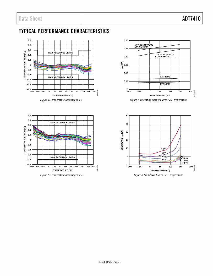
TYPICAL PERFORMANCE CHARACTERISTICS
0656
0-00
6
–60 –40 –20 0 20 40 60 80 100 120 140 160
TEM
PER
ATU
RE
ERR
OR
(°C
)
TEMPERATURE (°C)
–1.0
–0.8
–0.6
–0.4
–0.2
0
0.2
0.4
0.6
0.8
1.0
MAX ACCURACY LIMITS
MAX ACCURACY LIMITS
Figure 5. Temperature Accuracy at 3 V 06
560-
024
–1.0
–0.8
–0.6
–0.4
–0.2
0
0.2
0.4
0.6
0.8
1.0
–60 –40 –20 0 20 40 60 80 100 120 140 160
TEM
PER
ATU
RE
ERR
OR
(°C
)
TEMPERATURE (°C)
MAX ACCURACY LIMITS
MAX ACCURACY LIMITS
Figure 6. Temperature Accuracy at 5 V
0
0.05
0.10
0.15
0.20
0.25
0.30
–100 –50 0 50 100 150 200
I DD
(mA
)
TEMPERATURE (°C)
3.0V 1SPS
5.5V 1SPS
5.5V CONTINUOUSCONVERSION
3.0V CONTINUOUSCONVERSION
0656
0-00
7
Figure 7. Operating Supply Current vs. Temperature
3.6V
0656
0-02
5
SHU
TDO
WN
I DD
(µA
)
TEMPERATURE (°C)
0
5
10
15
20
25
30
–100 –50 0 50 100 150 200
3.3V3.0V2.7V
4.5V5.0V
5.5V
Figure 8. Shutdown Current vs. Temperature
ADT7410 Data Sheet
Rev. C | Page 8 of 24
0
0.05
0.10
0.15
0.20
0.25
0.30
2.5 3.0 3.5 4.0 4.5 5.0 5.5 6.0
I DD
(mA
)
SUPPLY VOLTAGE (V)
IDD CONTINUOUS CONVERSION
IDD 1SPS
0656
0-00
8
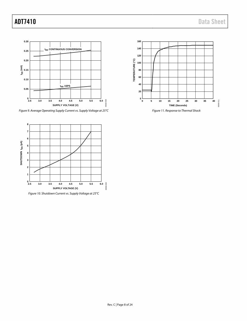
Figure 9. Average Operating Supply Current vs. Supply Voltage at 25°C
0
1
2
3
4
5
6
7
8
2.5 3.0 3.5 4.0 4.5 5.0 5.5 6.0
SHU
TDO
WN
IDD
(µA
)
SUPPLY VOLTAGE (V) 0656
0-00
9
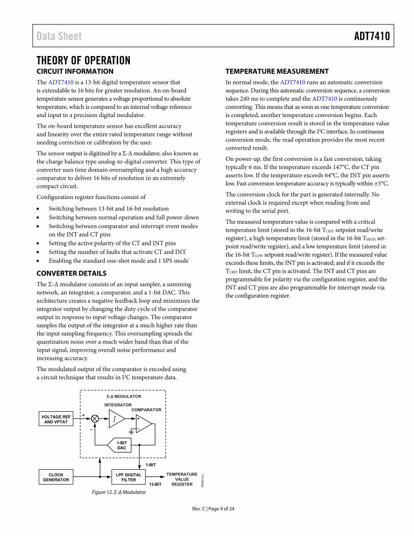
Figure 10. Shutdown Current vs. Supply Voltage at 25°C
0
20
40
60
80
100
120
140
160
0 403530252015105
TEM
PER
ATU
RE
(°C
)
TIME (Seconds) 0656
0-01
1
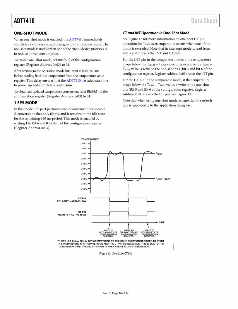
Figure 11. Response to Thermal Shock
Data Sheet ADT7410
Rev. C | Page 9 of 24
THEORY OF OPERATION CIRCUIT INFORMATION The ADT7410 is a 13-bit digital temperature sensor that is extendable to 16 bits for greater resolution. An on-board temperature sensor generates a voltage proportional to absolute temperature, which is compared to an internal voltage reference and input to a precision digital modulator.
The on-board temperature sensor has excellent accuracy and linearity over the entire rated temperature range without needing correction or calibration by the user.
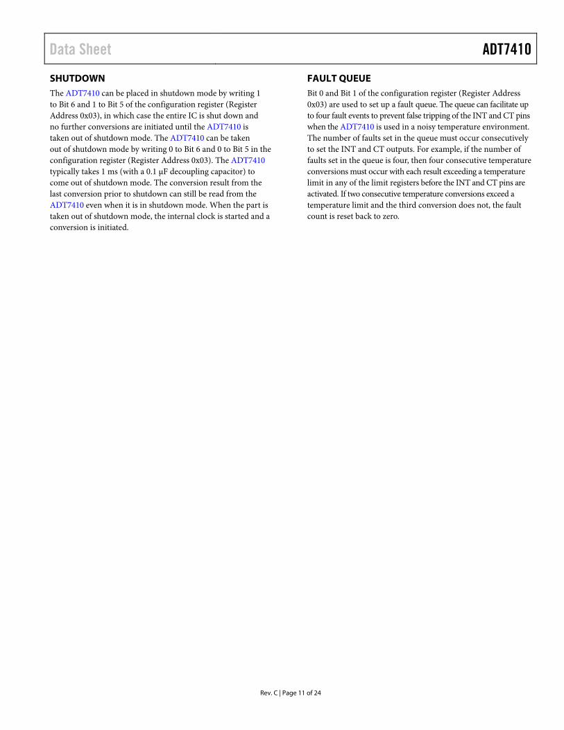
The sensor output is digitized by a Σ-Δ modulator, also known as the charge balance type analog-to-digital converter. This type of converter uses time domain oversampling and a high accuracy comparator to deliver 16 bits of resolution in an extremely compact circuit.
Configuration register functions consist of
Switching between 13-bit and 16-bit resolution Switching between normal operation and full power-down Switching between comparator and interrupt event modes
on the INT and CT pins Setting the active polarity of the CT and INT pins Setting the number of faults that activate CT and INT Enabling the standard one-shot mode and 1 SPS mode
CONVERTER DETAILS The Σ-Δ modulator consists of an input sampler, a summing network, an integrator, a comparator, and a 1-bit DAC. This architecture creates a negative feedback loop and minimizes the integrator output by changing the duty cycle of the comparator output in response to input voltage changes. The comparator samples the output of the integrator at a much higher rate than the input sampling frequency. This oversampling spreads the quantization noise over a much wider band than that of the input signal, improving overall noise performance and increasing accuracy.
The modulated output of the comparator is encoded using a circuit technique that results in I2C temperature data.
Σ-∆ MODULATOR
INTEGRATORCOMPARATOR
TEMPERATUREVALUE
REGISTER
CLOCKGENERATOR
LPF DIGITALFILTER
1-BITDAC
VOLTAGE REFAND VPTAT
1-BIT
13-BIT 0656
0-01
2
Figure 12. Σ-Δ Modulator
TEMPERATURE MEASUREMENT In normal mode, the ADT7410 runs an automatic conversion sequence. During this automatic conversion sequence, a conversion takes 240 ms to complete and the ADT7410 is continuously converting. This means that as soon as one temperature conversion is completed, another temperature conversion begins. Each temperature conversion result is stored in the temperature value registers and is available through the I2C interface. In continuous conversion mode, the read operation provides the most recent converted result.
On power-up, the first conversion is a fast conversion, taking typically 6 ms. If the temperature exceeds 147°C, the CT pin asserts low. If the temperature exceeds 64°C, the INT pin asserts low. Fast conversion temperature accuracy is typically within ±5°C.
The conversion clock for the part is generated internally. No external clock is required except when reading from and writing to the serial port.
The measured temperature value is compared with a critical temperature limit (stored in the 16-bit TCRIT setpoint read/write register), a high temperature limit (stored in the 16-bit THIGH set-point read/write register), and a low temperature limit (stored in the 16-bit TLOW setpoint read/write register). If the measured value exceeds these limits, the INT pin is activated; and if it exceeds the TCRIT limit, the CT pin is activated. The INT and CT pins are programmable for polarity via the configuration register, and the INT and CT pins are also programmable for interrupt mode via the configuration register.
ADT7410 Data Sheet
Rev. C | Page 10 of 24
ONE-SHOT MODE When one-shot mode is enabled, the ADT7410 immediately completes a conversion and then goes into shutdown mode. The one-shot mode is useful when one of the circuit design priorities is to reduce power consumption.
To enable one-shot mode, set Bits[6:5] of the configuration register (Register Address 0x03) to 01.
After writing to the operation mode bits, wait at least 240 ms before reading back the temperature from the temperature value register. This delay ensures that the ADT7410 has adequate time to power up and complete a conversion.
To obtain an updated temperature conversion, reset Bits[6:5] of the configuration register (Register Address 0x03) to 01.
1 SPS MODE In this mode, the part performs one measurement per second. A conversion takes only 60 ms, and it remains in the idle state for the remaining 940 ms period. This mode is enabled by writing 1 to Bit 6 and 0 to Bit 5 of the configuration register (Register Address 0x03).
CT and INT Operation in One-Shot Mode
See Figure 13 for more information on one-shot CT pin operation for TCRIT overtemperature events when one of the limits is exceeded. Note that in interrupt mode, a read from any register resets the INT and CT pins.
For the INT pin in the comparator mode, if the temperature drops below the THIGH − THYST value or goes above the TLOW + THYST value, a write to the one-shot bits (Bit 5 and Bit 6 of the configuration register, Register Address 0x03) resets the INT pin.
For the CT pin in the comparator mode, if the temperature drops below the TCRIT − THYST value, a write to the one-shot bits (Bit 5 and Bit 6 of the configuration register, Register Address 0x03) resets the CT pin. See Figure 13.
Note that when using one-shot mode, ensure that the refresh rate is appropriate to the application being used.
TEMPERATURE
149°C
148°C
147°C
146°C
145°C
144°C
143°C
142°C
141°C
140°C
CT PINPOLARITY = ACTIVE LOW
CT PINPOLARITY = ACTIVE HIGH
TCRIT
TCRIT – THYST
TIME
*THERE IS A 240ms DELAY BETWEEN WRITING TO THE CONFIGURATION REGISTER TO STARTA STANDARD ONE-SHOT CONVERSION AND THE CT PIN GOING ACTIVE. THIS IS DUE TO THECONVERSION TIME. THE DELAY IS 60ms IN THE CASE OF A 1 SPS CONVERSION.
WRITE TOBIT 5 AND BIT 6 OF
CONFIGURATIONREGISTER.*
WRITE TOBIT 5 AND BIT 6 OF
CONFIGURATIONREGISTER.*
WRITE TOBIT 5 AND BIT 6 OF
CONFIGURATIONREGISTER.*
0656
0-01
3
Figure 13. One-Shot CT Pin
Data Sheet ADT7410
Rev. C | Page 11 of 24
SHUTDOWN The ADT7410 can be placed in shutdown mode by writing 1 to Bit 6 and 1 to Bit 5 of the configuration register (Register Address 0x03), in which case the entire IC is shut down and no further conversions are initiated until the ADT7410 is taken out of shutdown mode. The ADT7410 can be taken out of shutdown mode by writing 0 to Bit 6 and 0 to Bit 5 in the configuration register (Register Address 0x03). The ADT7410 typically takes 1 ms (with a 0.1 µF decoupling capacitor) to come out of shutdown mode. The conversion result from the last conversion prior to shutdown can still be read from the ADT7410 even when it is in shutdown mode. When the part is taken out of shutdown mode, the internal clock is started and a conversion is initiated.
FAULT QUEUE Bit 0 and Bit 1 of the configuration register (Register Address 0x03) are used to set up a fault queue. The queue can facilitate up to four fault events to prevent false tripping of the INT and CT pins when the ADT7410 is used in a noisy temperature environment. The number of faults set in the queue must occur consecutively to set the INT and CT outputs. For example, if the number of faults set in the queue is four, then four consecutive temperature conversions must occur with each result exceeding a temperature limit in any of the limit registers before the INT and CT pins are activated. If two consecutive temperature conversions exceed a temperature limit and the third conversion does not, the fault count is reset back to zero.
ADT7410 Data Sheet
Rev. C | Page 12 of 24
TEMPERATURE DATA FORMAT One LSB of the ADC corresponds to 0.0625°C in 13-bit mode. The ADC can theoretically measure a temperature range of 255°C, but the ADT7410 is guaranteed to measure a low value temperature limit of −55°C to a high value temperature limit of +150°C. The temperature measurement result is stored in the 16-bit temperature value register and is compared with the high temperature limits stored in the TCRIT setpoint register and the THIGH setpoint register. It is also compared with the low temperature limit stored in the TLOW setpoint register.
Temperature data in the temperature value register, the TCRIT setpoint register, the THIGH setpoint register, and the TLOW setpoint register are represented by a 13-bit twos complement word. The MSB is the temperature sign bit. The three LSBs, Bit 0 to Bit 2, on power-up, are not part of the temperature conver-sion result and are flag bits for TCRIT, THIGH, and TLOW. Table 5 shows the 13-bit temperature data format without Bit 0 to Bit 2.
The number of bits in the temperature data-word can be extended to 16 bits, twos complement, by setting Bit 7 to 1 in the confi-guration register (Register Address 0x03). When using a 16-bit temperature data value, Bit 0 to Bit 2 are not used as flag bits and are, instead, the LSB bits of the temperature value. The power-on default setting has a 13-bit temperature data value.
Reading back the temperature from the temperature value register requires a 2-byte read. Designers that use a 9-bit temperature data format can still use the ADT7410 by ignoring the last four LSBs of the 13-bit temperature value. These four LSBs are Bit 6 to Bit 3 in Table 5.
Table 5. 13-Bit Temperature Data Format
Temperature Digital Output (Binary) Bits[15:3] Digital Output (Hex)
−55°C 1 1100 1001 0000 0x1C90 −50°C 1 1100 1110 0000 0x1CE0 −25°C 1 1110 0111 0000 0x1E70 −0.0625°C 1 1111 1111 1111 0x1FFF 0°C 0 0000 0000 0000 0x000 +0.0625°C 0 0000 0000 0001 0x001 +25°C 0 0001 1001 0000 0x190 +50°C 0 0011 0010 0000 0x320 +125°C 0 0111 1101 0000 0x7D0 +150°C 0 1001 0110 0000 0x960
TEMPERATURE CONVERSION FORMULAS 16-Bit Temperature Data Format
Positive Temperature = ADC Code (dec)/128
Negative Temperature = (ADC Code (dec) − 65,536)/128
where ADC Code uses all 16 bits of the data byte, including the sign bit.
Negative Temperature = (ADC Code (dec) − 32,768)/128
where Bit 15 (sign bit) is removed from the ADC code.
13-Bit Temperature Data Format Positive Temperature = ADC Code (dec)/16
Negative Temperature = (ADC Code (dec) − 8192)/16
where ADC Code uses the first 13 MSBs of the data byte, including the sign bit.
Negative Temperature = (ADC Code (dec) − 4096)/16
where Bit 15 (sign bit) is removed from the ADC code.
10-Bit Temperature Data Format Positive Temperature = ADC Code (dec)/2
Negative Temperature = (ADC Code (dec) − 1024)/2
where ADC Code uses all 10 bits of the data byte, including the sign bit.
Negative Temperature = (ADC Code (dec) − 512)/2
where Bit 9 (sign bit) is removed from the ADC code.
9-Bit Temperature Data Format Positive Temperature = ADC Code (dec)
Negative Temperature = ADC Code (dec) − 512
where ADC Code uses all nine bits of the data byte, including the sign bit.
Negative Temperature = ADC Code (dec) − 256
where Bit 8 (sign bit) is removed from the ADC code.
Data Sheet ADT7410
Rev. C | Page 13 of 24
REGISTERS The ADT7410 contains 14 registers: • Nine temperature registers • A status register • An ID register • A configuration register • An address pointer register • A software reset All registers are eight bits wide. The temperature value registers, the status register, and the ID register are read-only. The software reset is a write-only register. On power-up, the address pointer register is loaded with 0x00 and points to the temperature value register MSB.
Table 6. ADT7410 Registers Register Address Description
Power-On Default
0x00 Temperature value most significant byte 0x00 0x01 Temperature value least significant byte 0x00 0x02 Status 0x00 0x03 Configuration 0x00 0x04 THIGH setpoint most significant byte 0x20 (64°C) 0x05 THIGH setpoint least significant byte 0x00 (64°C) 0x06 TLOW setpoint most significant byte 0x05 (10°C) 0x07 TLOW setpoint least significant byte 0x00 (10°C) 0x08 TCRIT setpoint most significant byte 0x49 (147°C) 0x09 TCRIT setpoint least significant byte 0x80 (147°C) 0x0A THYST setpoint 0x05 (5°C) 0x0B ID 0xCX 0x0C Reserved 0xXX 0x0D Reserved 0xXX 0x2E Reserved 0xXX 0x2F Software reset 0xXX
ADDRESS POINTER REGISTER This register is always the first register written to during a write to the ADT7410. It must be set to the address of the register to which the write or read transaction is intended. Table 7 shows the register address of each register on the ADT7410. The default value of the address pointer register is 0x00.
Table 7. Address Pointer Register P7 P6 P5 P4 P3 P2 P1 P0 ADD7 ADD6 ADD5 ADD4 ADD3 ADD2 ADD1 ADD0
TEMPERATURE VALUE REGISTERS The temperature value most significant byte (MSB) and tem-perature value least significant byte (LSB) registers store the temperature measured by the internal temperature sensor. The temperature is stored in twos complement format with the MSB being the temperature sign bit. When reading from these registers, the eight MSBs (Bit 7 to Bit 15) are read first from Register Address 0x00 and then the eight LSBs (Bit 0 to Bit 7) are read from Register Address 0x01. Only the temperature value most significant byte (Register Address 0x00) needs to be loaded into the address pointer register as the address pointer auto-increments to the temperature value least significant byte address (Register Address 0x01).
Bit 0 to Bit 2 are event alarm flags for TCRIT, THIGH, and TLOW. When the ADC is configured to convert the temperature to a 16-bit digital value then Bit 0 to Bit 2 are no longer used as flag bits and are instead used as the LSB bits for the extended digital value.
Table 8. Temperature Value MSB Register (Register Address 0x00) Bit Default Value Type Name Description [14:8] 0000000 R Temp Temperature value in twos complement format
15 0 R Sign Sign bit, indicates if the temperature value is negative or positive
Table 9. Temperature Value LSB Register (Register Address 0x01) Bit Default Value Type Name Description 0 0 R TLOW flag/LSB0 Flags a TLOW event if the configuration register, Register Address 0x03[7] = 0 (13-bit resolution),
and if comparator mode is selected through the configuration register, Register Address 0x03[4]. When the temperature value is below TLOW, this bit it set to 1.
Contains the Least Significant Bit 0 of the 15-bit temperature value if the configuration register, Register Address 0x03[7] = 1 (16-bit resolution).
1 0 R THIGH flag/LSB1 Flags a THIGH event if the configuration register, Register Address 0x03[7] = 0 (13-bit resolution), and if comparator mode is selected through the configuration register, Register Address 0x03[4]. When the temperature value is above THIGH, this bit it set to 1.
Contains the Least Significant Bit 1 of the 15-bit temperature value if the configuration register, Register Address 0x03[7] = 1 (16-bit resolution).
2 0 R TCRIT flag/LSB2 Flags a TCRIT event if the configuration register, Register Address 0x03[7] = 0 (13-bit resolution), and if comparator mode is selected through the configuration register, Register Address 0x03[4]. When the temperature value exceeds TCRIT, this bit it set to 1.
Contains the Least Significant Bit 2 of the 15-bit temperature value if the configuration register, Register Address 0x03[7] = 1 (16-bit resolution).
[7:3] 00000 R Temp Temperature value in twos complement format.
ADT7410 Data Sheet
Rev. C | Page 14 of 24
STATUS REGISTER This 8-bit read-only register reflects the status of the overtempera-ture and undertemperature interrupts that can cause the CT and INT pins to go active. It also reflects the status of a temperature conversion operation. The interrupt flags in this register are reset by a read operation to the status register and/or when the temperature value returns within the temperature limits, including hysteresis. The RDY bit is reset after a read from the
temperature value register. In one-shot and 1 SPS modes, the RDY bit is reset after a write to the one-shot bits.
CONFIGURATION REGISTER This 8-bit read/write register stores various configuration modes for the ADT7410, including shutdown, overtemperature and undertemperature interrupts, one-shot, continuous conversion, interrupt pins polarity, and overtemperature fault queues.
Table 10. Status Register (Register Address 0x02) Bit Default Value Type Name Description [3:0] 0000 R Unused Reads back 0. 4 0 R TLOW Set this bit to 1 when the temperature goes below the TLOW temperature limit, and if comparator
mode is selected through the configuration register, Register Address 0x03[4]. The bit clears to 0 when the status register is read and/or when the temperature measured goes back above the limit set in the setpoint TLOW + THYST registers.
5 0 R THIGH Set this bit to 1 when the temperature goes above the THIGH temperature limit, and if comparator mode is selected through the configuration register, Register Address 0x03[4]. The bit clears to 0 when the status register is read and/or when the temperature measured goes back below the limit set in the setpoint THIGH − THYST registers.
6 0 R TCRIT Set this bit to 1 when the temperature goes above the TCRIT temperature limit, and if comparator mode is selected through the configuration register, Register Address 0x03[4]. This bit clears to 0 when the status register is read and/or when the temperature measured goes back below the limit set in the setpoint TCRIT − THYST registers.
7 1 R RDY This bit goes low when the temperature conversion result is written into the temperature value register. It is reset to 1 when the temperature value register is read. In one-shot and 1 SPS modes, this bit is reset after a write to the one-shot bits.
Table 11. Configuration Register (Register Address 0x03) Bit Default Value Type Name Description [1:0] 00 R/W Fault queue These two bits set the number of undertemperature/overtemperature faults that can
occur before setting the INT and CT pins. This helps to avoid false triggering due to temperature noise.
00 = 1 fault (default). 01 = 2 faults. 10 = 3 faults. 11 = 4 faults. 2 0 R/W CT pin polarity This bit selects the output polarity of the CT pin.
0 = active low. 1 = active high. 3 0 R/W INT pin polarity This bit selects the output polarity of the INT pin.
0 = active low. 1 = active high. 4 0 R/W INT/CT mode This bit selects between comparator mode and interrupt mode.
0 = interrupt mode 1 = comparator mode [6:5] 00 R/W Operation mode These two bits set the operational mode for the ADT7410.
00 = continuous conversion (default). When one conversion is finished, the ADT7410 starts another.
01 = one shot. Conversion time is typically 240 ms. 10 = 1 SPS mode. Conversion time is typically 60 ms. This operational mode
reduces the average current consumption. 11 = shutdown. All circuitry except interface circuitry is powered down. 7 0 R/W Resolution This bit sets up the resolution of the ADC when converting.
0 = 13-bit resolution. Sign bit + 12 bits gives a temperature resolution of 0.0625°C. 1 = 16-bit resolution. Sign bit + 15 bits gives a temperature resolution of 0.0078°C.
Data Sheet ADT7410
Rev. C | Page 15 of 24
THIGH SETPOINT REGISTERS The THIGH setpoint MSB and THIGH setpoint LSB registers store the overtemperature limit value. An overtemperature event occurs when the temperature value stored in the temperature value register exceeds the value stored in this register. The INT pin is activated if an overtemperature event occurs. The temperature is stored in twos complement format with the MSB being the temperature sign bit.
When reading from this register, the eight MSBs (Bit 15 to Bit 8) are read first from Register Address 0x04 and then the eight LSBs (Bit 7 to Bit 0) are read from Register Address 0x05. Only Register Address 0x04 (THIGH setpoint MSB) needs to be loaded into the address pointer register as the address pointer auto-increments to Register Address 0x05 (THIGH setpoint LSB).
The default setting for the THIGH setpoint is 64°C.
TLOW SETPOINT REGISTERS The TLOW setpoint MSB and TLOW setpoint LSB registers store the undertemperature limit value. An undertemperature event occurs when the temperature value stored in the temperature value register is less than the value stored in this register. The INT pin is activated if an undertemperature event occurs. The temperature is stored in twos complement format with the MSB being the temperature sign bit.
When reading from this register, the eight MSBs (Bit 15 to Bit 8) are read first from Register Address 0x06 and then the eight LSBs (Bit 7 to Bit 0) are read from Register Address 0x07. Only the Register Address 0x06 (TLOW setpoint MSB) needs to be loaded into the address pointer register as the address pointer auto-increments to Register Address 0x07 (TLOW setpoint LSB).
The default setting for the TLOW setpoint is 10°C.
TCRIT SETPOINT REGISTERS The TCRIT setpoint MSB and TCRIT setpoint LSB registers store the critical overtemperature limit value. A critical overtemperature event occurs when the temperature value stored in the temperature value register exceeds the value stored in this register. The CT pin is activated if a critical overtemperature event occurs. The temperature is stored in twos complement format with the MSB being the temperature sign bit.
When reading from this register, the eight MSBs (Bit 15 to Bit 8) are read first from Register Address 0x08 and then the eight LSBs (Bit 7 to Bit 0) are read from Register Address 0x09. Only the Register Address 0x08 (TCRIT setpoint MSB) needs to be loaded into the address pointer register as the address pointer auto-increments to Register Address 0x09 (TCRIT setpoint LSB).
The default setting for the TCRIT limit is 147°C.
Table 12. THIGH Setpoint MSB Register (Register Address 0x04) Bit Default Value Type Name Description
[15:8] 0x20 R/W THIGH MSB MSBs of the overtemperature limit, stored in twos complement format.
Table 13. THIGH Setpoint LSB Register (Register Address 0x05) Bit Default Value Type Name Description
[7:0] 0x00 R/W THIGH LSB LSBs of the overtemperature limit, stored in twos complement format.
Table 14. TLOW Setpoint MSB Register (Register Address 0x06) Bit Default Value Type Name Description
[15:8] 0x05 R/W TLOW MSB MSBs of the undertemperature limit, stored in twos complement format.
Table 15. TLOW Setpoint LSB Register (Register Address 0x07) Bit Default Value Type Name Description
[7:0] 0x00 R/W TLOW LSB LSBs of the undertemperature limit, stored in twos complement format.
Table 16. TCRIT Setpoint MSB Register (Register Address 0x08) Bit Default Value Type Name Description
[15:8] 0x49 R/W TCRIT MSB MSBs of the critical overtemperature limit, stored in twos complement format.
Table 17. TCRIT Setpoint LSB Register (Register Address 0x09) Bit Default Value Type Name Description
[7:0] 0x80 R/W TCRIT LSB LSBs of the critical overtemperature limit, stored in twos complement format.
ADT7410 Data Sheet
Rev. C | Page 16 of 24
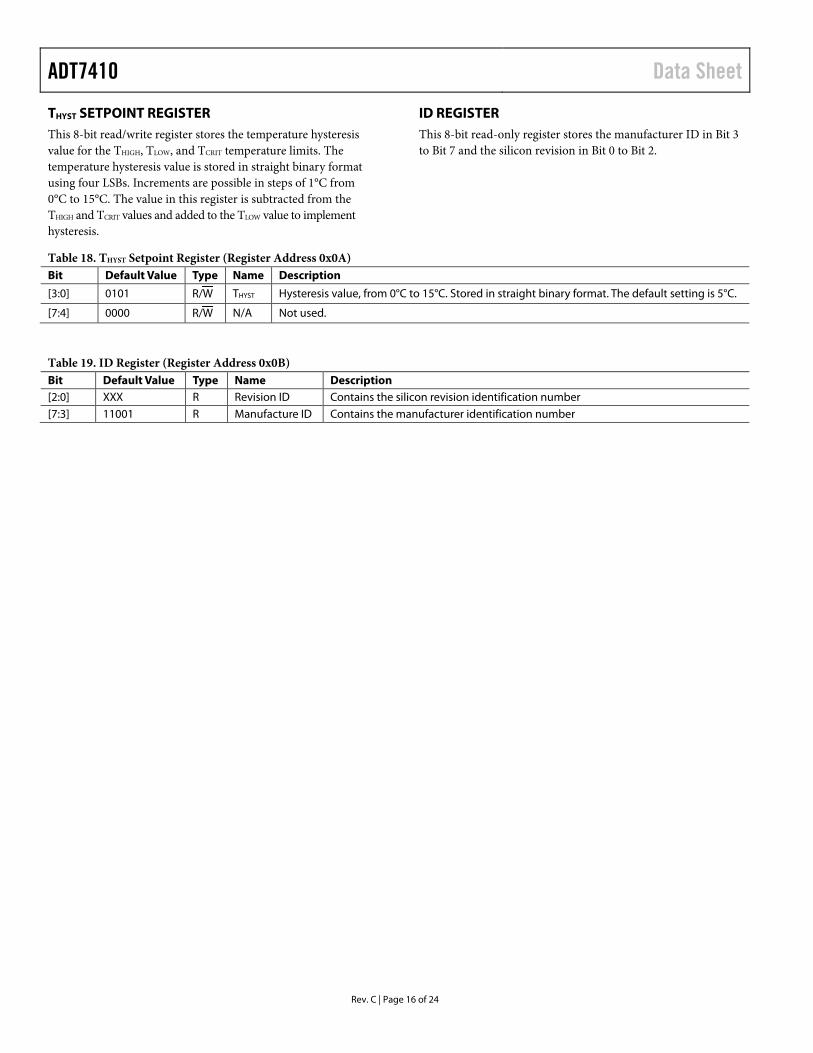
THYST SETPOINT REGISTER This 8-bit read/write register stores the temperature hysteresis value for the THIGH, TLOW, and TCRIT temperature limits. The temperature hysteresis value is stored in straight binary format using four LSBs. Increments are possible in steps of 1°C from 0°C to 15°C. The value in this register is subtracted from the THIGH and TCRIT values and added to the TLOW value to implement hysteresis.
ID REGISTER This 8-bit read-only register stores the manufacturer ID in Bit 3 to Bit 7 and the silicon revision in Bit 0 to Bit 2.
Table 18. THYST Setpoint Register (Register Address 0x0A) Bit Default Value Type Name Description
[3:0] 0101 R/W THYST Hysteresis value, from 0°C to 15°C. Stored in straight binary format. The default setting is 5°C.
[7:4] 0000 R/W N/A Not used.
Table 19. ID Register (Register Address 0x0B) Bit Default Value Type Name Description [2:0] XXX R Revision ID Contains the silicon revision identification number [7:3] 11001 R Manufacture ID Contains the manufacturer identification number
Data Sheet ADT7410
Rev. C | Page 17 of 24
SERIAL INTERFACE
ADT7410
SCLCT
INT
A1A0
SDA
GND
VDD
10kΩ10kΩ10kΩ
PULL-UPVDD
PULL-UPVDD
0.1µF10kΩ
PULL-UPVDD
TO INTERRUPT PINON MICROCONTROLLER
VDD
0656
0-01
4
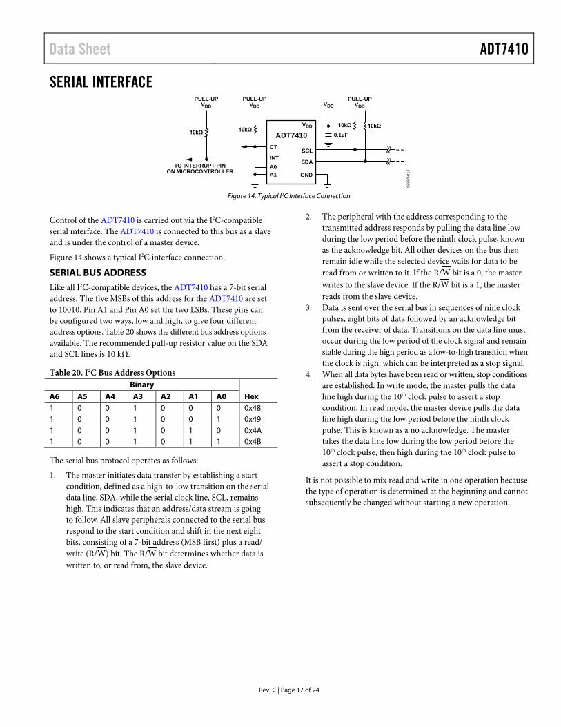
Figure 14. Typical I2C Interface Connection
Control of the ADT7410 is carried out via the I2C-compatible serial interface. The ADT7410 is connected to this bus as a slave and is under the control of a master device.
Figure 14 shows a typical I2C interface connection.
SERIAL BUS ADDRESS Like all I2C-compatible devices, the ADT7410 has a 7-bit serial address. The five MSBs of this address for the ADT7410 are set to 10010. Pin A1 and Pin A0 set the two LSBs. These pins can be configured two ways, low and high, to give four different address options. Table 20 shows the different bus address options available. The recommended pull-up resistor value on the SDA and SCL lines is 10 kΩ.
Table 20. I2C Bus Address Options Binary
Hex A6 A5 A4 A3 A2 A1 A0 1 0 0 1 0 0 0 0x48 1 0 0 1 0 0 1 0x49 1 0 0 1 0 1 0 0x4A 1 0 0 1 0 1 1 0x4B
The serial bus protocol operates as follows:
1. The master initiates data transfer by establishing a start condition, defined as a high-to-low transition on the serial data line, SDA, while the serial clock line, SCL, remains high. This indicates that an address/data stream is going to follow. All slave peripherals connected to the serial bus respond to the start condition and shift in the next eight bits, consisting of a 7-bit address (MSB first) plus a read/ write (R/W) bit. The R/W bit determines whether data is written to, or read from, the slave device.
2. The peripheral with the address corresponding to the transmitted address responds by pulling the data line low during the low period before the ninth clock pulse, known as the acknowledge bit. All other devices on the bus then remain idle while the selected device waits for data to be read from or written to it. If the R/W bit is a 0, the master writes to the slave device. If the R/W bit is a 1, the master reads from the slave device.
3. Data is sent over the serial bus in sequences of nine clock pulses, eight bits of data followed by an acknowledge bit from the receiver of data. Transitions on the data line must occur during the low period of the clock signal and remain stable during the high period as a low-to-high transition when the clock is high, which can be interpreted as a stop signal.
4. When all data bytes have been read or written, stop conditions are established. In write mode, the master pulls the data line high during the 10th clock pulse to assert a stop condition. In read mode, the master device pulls the data line high during the low period before the ninth clock pulse. This is known as a no acknowledge. The master takes the data line low during the low period before the 10th clock pulse, then high during the 10th clock pulse to assert a stop condition.
It is not possible to mix read and write in one operation because the type of operation is determined at the beginning and cannot subsequently be changed without starting a new operation.
ADT7410 Data Sheet
Rev. C | Page 18 of 24
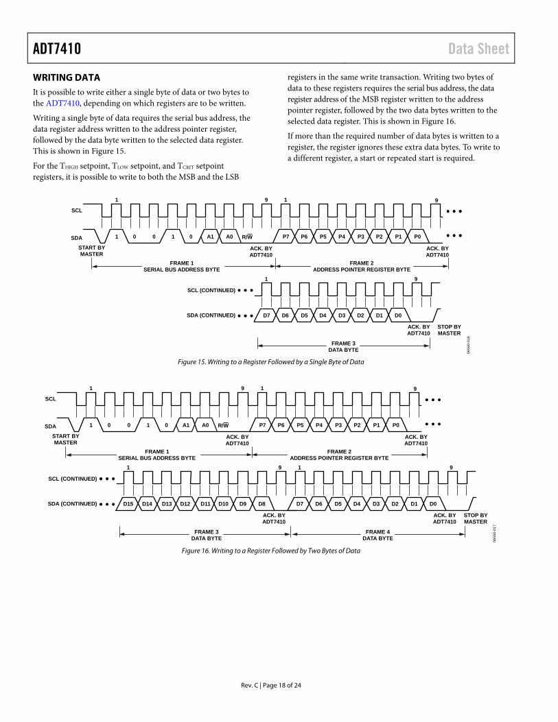
WRITING DATA It is possible to write either a single byte of data or two bytes to the ADT7410, depending on which registers are to be written.
Writing a single byte of data requires the serial bus address, the data register address written to the address pointer register, followed by the data byte written to the selected data register. This is shown in Figure 15.
For the THIGH setpoint, TLOW setpoint, and TCRIT setpoint registers, it is possible to write to both the MSB and the LSB
registers in the same write transaction. Writing two bytes of data to these registers requires the serial bus address, the data register address of the MSB register written to the address pointer register, followed by the two data bytes written to the selected data register. This is shown in Figure 16.
If more than the required number of data bytes is written to a register, the register ignores these extra data bytes. To write to a different register, a start or repeated start is required.
FRAME 1SERIAL BUS ADDRESS BYTE
FRAME 2ADDRESS POINTER REGISTER BYTE
ACK. BYADT7410
ACK. BYADT7410
ACK. BYADT7410
STOP BYMASTER
FRAME 3DATA BYTE
SDA (CONTINUED)
SCL (CONTINUED)
SCL
SDA
START BYMASTER
1 0 0 1 0 A1 A0 P7 P6 P5 P4 P3 P2 P1 P0
9
D7 D6 D5 D4 D3 D2 D1 D0
R/W
191
91
0656
0-01
6
Figure 15. Writing to a Register Followed by a Single Byte of Data
FRAME 1SERIAL BUS ADDRESS BYTE
FRAME 2ADDRESS POINTER REGISTER BYTE
ACK. BYADT7410
ACK. BYADT7410
ACK. BYADT7410
STOP BYMASTER
FRAME 4DATA BYTE
SCL
SDA
START BYMASTER
1 0 0 1 0 A1 A0 P7 P6 P5 P4 P3 P2 P1 P0
9
D7 D6 D5 D4 D3 D2 D1 D0
R/W
191
91
ACK. BYADT7410
FRAME 3DATA BYTE
SDA (CONTINUED)
SCL (CONTINUED)
D15 D14 D13 D12 D11 D10 D9 D8
91
0656
0-01
7
Figure 16. Writing to a Register Followed by Two Bytes of Data
Data Sheet ADT7410
Rev. C | Page 19 of 24
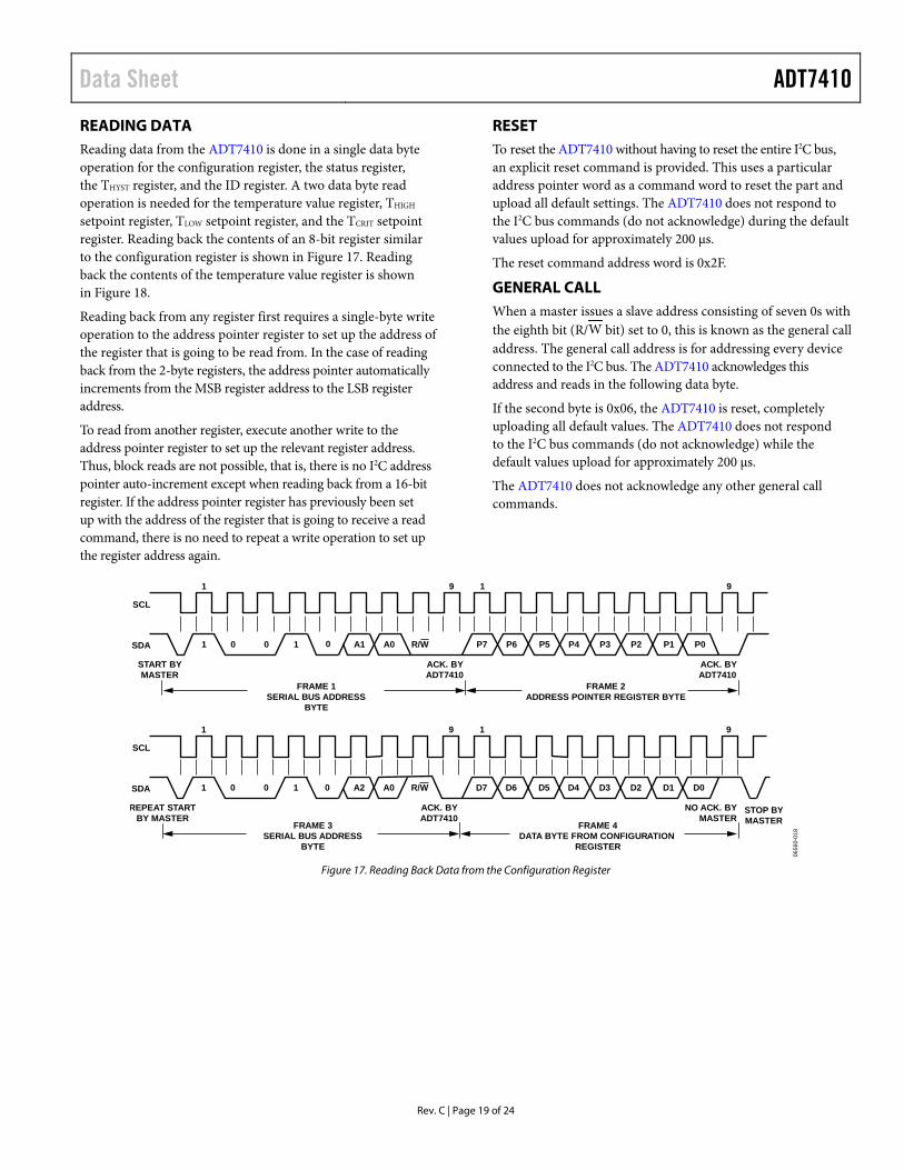
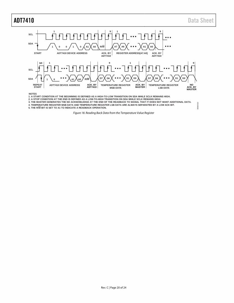
READING DATA Reading data from the ADT7410 is done in a single data byte operation for the configuration register, the status register, the THYST register, and the ID register. A two data byte read operation is needed for the temperature value register, THIGH setpoint register, TLOW setpoint register, and the TCRIT setpoint register. Reading back the contents of an 8-bit register similar to the configuration register is shown in Figure 17. Reading back the contents of the temperature value register is shown in Figure 18.
Reading back from any register first requires a single-byte write operation to the address pointer register to set up the address of the register that is going to be read from. In the case of reading back from the 2-byte registers, the address pointer automatically increments from the MSB register address to the LSB register address.
To read from another register, execute another write to the address pointer register to set up the relevant register address. Thus, block reads are not possible, that is, there is no I2C address pointer auto-increment except when reading back from a 16-bit register. If the address pointer register has previously been set up with the address of the register that is going to receive a read command, there is no need to repeat a write operation to set up the register address again.
RESET To reset the ADT7410 without having to reset the entire I2C bus, an explicit reset command is provided. This uses a particular address pointer word as a command word to reset the part and upload all default settings. The ADT7410 does not respond to the I2C bus commands (do not acknowledge) during the default values upload for approximately 200 µs.
The reset command address word is 0x2F.
GENERAL CALL When a master issues a slave address consisting of seven 0s with the eighth bit (R/W bit) set to 0, this is known as the general call address. The general call address is for addressing every device connected to the I2C bus. The ADT7410 acknowledges this address and reads in the following data byte.
If the second byte is 0x06, the ADT7410 is reset, completely uploading all default values. The ADT7410 does not respond to the I2C bus commands (do not acknowledge) while the default values upload for approximately 200 µs.
The ADT7410 does not acknowledge any other general call commands.
SCL
SDA
1
1 0 0 1 A20 A0
REPEAT STARTBY MASTER
FRAME 3SERIAL BUS ADDRESS
BYTE
FRAME 4DATA BYTE FROM CONFIGURATION
REGISTER
STOP BYMASTER
ACK. BYADT7410
NO ACK. BYMASTER
R/W D7 D6 D5 D4 D3 D2 D1 D0
9 91
0656
0-01
8
SCL
SDA
1
1 0 0 1 A1 A0
START BYMASTER
FRAME 1SERIAL BUS ADDRESS
BYTE
FRAME 2ADDRESS POINTER REGISTER BYTE
ACK. BYADT7410
ACK. BYADT7410
R/W P7 P6 P5 P4 P3 P2 P1 P0
9 91
0
Figure 17. Reading Back Data from the Configuration Register
ADT7410 Data Sheet
Rev. C | Page 20 of 24
NOTES1. A START CONDITION AT THE BEGINNING IS DEFINED AS A HIGH-TO-LOW TRANSITION ON SDA WHILE SCLK REMAINS HIGH.2. A STOP CONDITION AT THE END IS DEFINED AS A LOW-TO-HIGH TRANSITION ON SDA WHILE SCLK REMAINS HIGH.3. THE MASTER GENERATES THE NO ACKNOWLEDGE AT THE END OF THE READBACK TO SIGNAL THAT IT DOES NOT WANT ADDITIONAL DATA.4. TEMPERATURE REGISTER MSB DATA AND TEMPERATURE REGISTER LSB DATA ARE ALWAYS SEPARATED BY A LOW ACK BIT.5. THE R/W BIT IS SET TO A1 TO INDICATE A READBACK OPERATION.
SDA1 0 0 R/W A7 A6
SCL
SDA
SCL
1 A1 A0
1 1
0 A1 A0
9
ADT7410 DEVICE ADDRESS REGISTER ADDRESS[A7:A0]
D1 D0D7 D6
TEMPERATURE REGISTERMSB DATA
9
1 19 9
01 A1 A0
0656
0-02
3
R/W
REPEATSTART
D1 D0D7 D6
ACK. BYADT7410
ACK. BYMASTER
NOACK. BYMASTER
ACK. BYADT7410
START
ADT7410 DEVICE ADDRESS ACK. BYADT7410
TEMPERATURE REGISTERLSB DATA
SR
Figure 18. Reading Back Data from the Temperature Value Register
Data Sheet ADT7410
Rev. C | Page 21 of 24
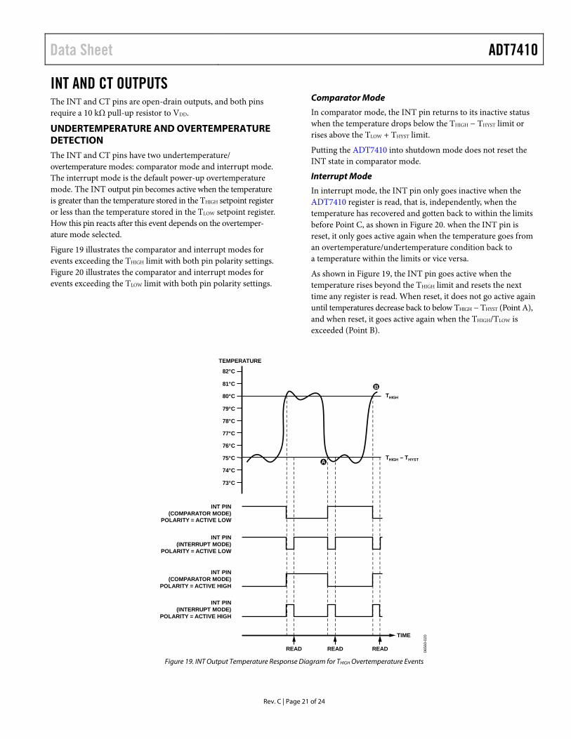
INT AND CT OUTPUTS The INT and CT pins are open-drain outputs, and both pins require a 10 kΩ pull-up resistor to VDD.
UNDERTEMPERATURE AND OVERTEMPERATURE DETECTION The INT and CT pins have two undertemperature/ overtemperature modes: comparator mode and interrupt mode. The interrupt mode is the default power-up overtemperature mode. The INT output pin becomes active when the temperature is greater than the temperature stored in the THIGH setpoint register or less than the temperature stored in the TLOW setpoint register. How this pin reacts after this event depends on the overtemper-ature mode selected.
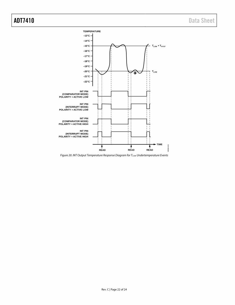
Figure 19 illustrates the comparator and interrupt modes for events exceeding the THIGH limit with both pin polarity settings. Figure 20 illustrates the comparator and interrupt modes for events exceeding the TLOW limit with both pin polarity settings.
Comparator Mode
In comparator mode, the INT pin returns to its inactive status when the temperature drops below the THIGH − THYST limit or rises above the TLOW + THYST limit.
Putting the ADT7410 into shutdown mode does not reset the INT state in comparator mode.
Interrupt Mode
In interrupt mode, the INT pin only goes inactive when the ADT7410 register is read, that is, independently, when the temperature has recovered and gotten back to within the limits before Point C, as shown in Figure 20. when the INT pin is reset, it only goes active again when the temperature goes from an overtemperature/undertemperature condition back to a temperature within the limits or vice versa.
As shown in Figure 19, the INT pin goes active when the temperature rises beyond the THIGH limit and resets the next time any register is read. When reset, it does not go active again until temperatures decrease back to below THIGH − THYST (Point A), and when reset, it goes active again when the THIGH/TLOW is exceeded (Point B).
TEMPERATURE
82°C
81°C
80°C
79°C
78°C
77°C
76°C
75°C
74°C
73°C
INT PIN(COMPARATOR MODE)
POLARITY = ACTIVE LOW
INT PIN(INTERRUPT MODE)
POLARITY = ACTIVE LOW
INT PIN(INTERRUPT MODE)
POLARITY = ACTIVE HIGH
INT PIN(COMPARATOR MODE)
POLARITY = ACTIVE HIGH
THIGH
THIGH – THYST
TIME
READ READ READ 0656
0-02
0
A
B
Figure 19. INT Output Temperature Response Diagram for THIGH Overtemperature Events
ADT7410 Data Sheet
Rev. C | Page 22 of 24
TEMPERATURE
–13°C
–14°C
–15°C
–16°C
–17°C
–18°C
–19°C
–20°C
–21°C
–22°C
INT PIN(COMPARATOR MODE)
POLARITY = ACTIVE LOW
INT PIN(INTERRUPT MODE)
POLARITY = ACTIVE LOW
INT PIN(INTERRUPT MODE)
POLARITY = ACTIVE HIGH
INT PIN(COMPARATOR MODE)
POLARITY = ACTIVE HIGH
TLOW + THYST
TLOW
TIME
READ READ READ 0656
0-02
1
C
Figure 20. INT Output Temperature Response Diagram for TLOW Undertemperature Events
Data Sheet ADT7410
Rev. C | Page 23 of 24
APPLICATIONS INFORMATION THERMAL RESPONSE TIME The time required for a temperature sensor to settle to a specified accuracy is a function of the thermal mass of the sensor and the thermal conductivity between the sensor and the object being sensed. Thermal mass is often considered equivalent to capacitance. Thermal conductivity is commonly specified using the symbol, Q, and can be thought of as thermal resistance. It is commonly specified in units of degrees per watt of power transferred across the thermal joint. The time required for the part to settle to the desired accuracy is dependent on the thermal contact established in a particular application and the equivalent power of the heat source. In most applications, it is best to determine the settling time empirically.
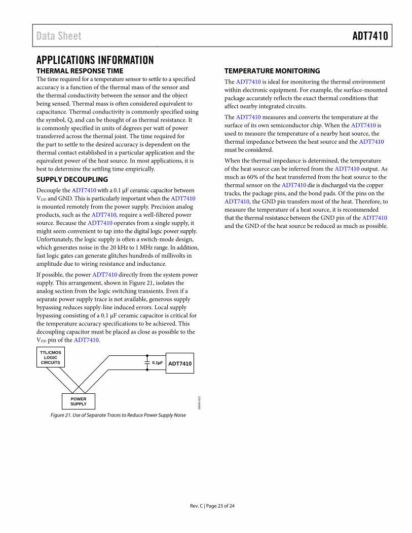
SUPPLY DECOUPLING Decouple the ADT7410 with a 0.1 µF ceramic capacitor between VDD and GND. This is particularly important when the ADT7410 is mounted remotely from the power supply. Precision analog products, such as the ADT7410, require a well-filtered power source. Because the ADT7410 operates from a single supply, it might seem convenient to tap into the digital logic power supply. Unfortunately, the logic supply is often a switch-mode design, which generates noise in the 20 kHz to 1 MHz range. In addition, fast logic gates can generate glitches hundreds of millivolts in amplitude due to wiring resistance and inductance.
If possible, the power ADT7410 directly from the system power supply. This arrangement, shown in Figure 21, isolates the analog section from the logic switching transients. Even if a separate power supply trace is not available, generous supply bypassing reduces supply-line induced errors. Local supply bypassing consisting of a 0.1 µF ceramic capacitor is critical for the temperature accuracy specifications to be achieved. This decoupling capacitor must be placed as close as possible to the VDD pin of the ADT7410.
0.1µF ADT7410
TTL/CMOSLOGIC
CIRCUITS
POWERSUPPLY
0656
0-02
2
Figure 21. Use of Separate Traces to Reduce Power Supply Noise
TEMPERATURE MONITORING The ADT7410 is ideal for monitoring the thermal environment within electronic equipment. For example, the surface-mounted package accurately reflects the exact thermal conditions that affect nearby integrated circuits.
The ADT7410 measures and converts the temperature at the surface of its own semiconductor chip. When the ADT7410 is used to measure the temperature of a nearby heat source, the thermal impedance between the heat source and the ADT7410 must be considered.
When the thermal impedance is determined, the temperature of the heat source can be inferred from the ADT7410 output. As much as 60% of the heat transferred from the heat source to the thermal sensor on the ADT7410 die is discharged via the copper tracks, the package pins, and the bond pads. Of the pins on the ADT7410, the GND pin transfers most of the heat. Therefore, to measure the temperature of a heat source, it is recommended that the thermal resistance between the GND pin of the ADT7410 and the GND of the heat source be reduced as much as possible.
ADT7410 Data Sheet
Rev. C | Page 24 of 24
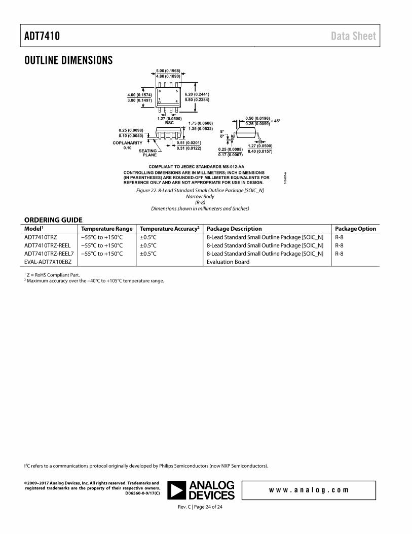
OUTLINE DIMENSIONS
CONTROLLING DIMENSIONS ARE IN MILLIMETERS; INCH DIMENSIONS(IN PARENTHESES) ARE ROUNDED-OFF MILLIMETER EQUIVALENTS FORREFERENCE ONLY AND ARE NOT APPROPRIATE FOR USE IN DESIGN.
COMPLIANT TO JEDEC STANDARDS MS-012-AA
012
407-
A
0.25 (0.0098)0.17 (0.0067)
1.27 (0.0500)0.40 (0.0157)
0.50 (0.0196)0.25 (0.0099)
45°
8°0°
1.75 (0.0688)1.35 (0.0532)
SEATINGPLANE
0.25 (0.0098)0.10 (0.0040)
41
8 5
5.00 (0.1968)4.80 (0.1890)
4.00 (0.1574)3.80 (0.1497)
1.27 (0.0500)BSC
6.20 (0.2441)5.80 (0.2284)
0.51 (0.0201)0.31 (0.0122)
COPLANARITY0.10
Figure 22. 8-Lead Standard Small Outline Package [SOIC_N]
Narrow Body (R-8)
Dimensions shown in millimeters and (inches)
ORDERING GUIDE Model1 Temperature Range Temperature Accuracy2 Package Description Package Option ADT7410TRZ −55°C to +150°C ±0.5°C 8-Lead Standard Small Outline Package [SOIC_N] R-8 ADT7410TRZ-REEL −55°C to +150°C ±0.5°C 8-Lead Standard Small Outline Package [SOIC_N] R-8 ADT7410TRZ-REEL7 −55°C to +150°C ±0.5°C 8-Lead Standard Small Outline Package [SOIC_N] R-8 EVAL-ADT7X10EBZ Evaluation Board 1 Z = RoHS Compliant Part. 2 Maximum accuracy over the −40°C to +105°C temperature range.
I2C refers to a communications protocol originally developed by Philips Semiconductors (now NXP Semiconductors).
©2009–2017 Analog Devices, Inc. All rights reserved. Trademarks and registered trademarks are the property of their respective owners. D06560-0-9/17(C)
Mouser Electronics
Authorized Distributor
Click to View Pricing, Inventory, Delivery & Lifecycle Information: Analog Devices Inc.:
EVAL-ADT7X10EBZ ADT7410TRZ-REEL7 ADT7410TRZ-REEL ADT7410TRZ EVAL-ADT7410MBZ