Embed Size (px)
Citation preview

5/14/2018 0471410160-1 - slidepdf.com
http://slidepdf.com/reader/full/0471410160-1 1/30
Integrated Circuit Design
with the MOSFET
9.1 MOSFET Current Mirrors
9.2 Amplifier Configurations for
MOSFET Integrated Circuits
The MOSFET has become more popular in circuit design in the last decade,
especially for mixed-signal circuits that combine both digital and analog circuits
on a single chip. With the improvements in high-frequency performance, the
MOSFET can compete with the BJT up to frequencies in the low GHz range.
Of course, the heterojunction BJT can operate at much higher frequencies than
this, approaching frequencies of 100 GHz.
This chapter will consider several configurations of amplifying stages used
in MOSFET amplifier design. Each configuration is analyzed in terms of mid-
band voltage gain, upper corner frequency, and the size of the output active
region.
Design of MOSFET circuits is considerably different from the design of
BJT circuits. For example, the dimensions of the channel are used as part of
the design procedure in MOSFET circuits. The width of the channel affects
the transconductance, the output resistance and capacitance, and the midband
voltage gain of the stage. The specification of channel width is often one step
in the design of a MOSFET amplifier stage. In digital circuits, the width and
the length are generally of the same order of magnitude. In amplifier design,
the dimension of channel width may be hundreds of times greater than the
channel length to achieve high values of voltage gain. Such considerations are
not necessary in BJT amplifier design, which provides one reason for cov-
ering BJT design in a separate chapter. The next chapter will consider the
BJT.
One circuit that is very significant in IC design is the current mirror. This
circuit not only provides bias for amplifier stages, it also provides an incremental
resistive load for various amplifier stages. The first section of this chapter will
discuss some basic configurations of this important circuit, before moving to
various amplifier configurations.
D E M O N S T R A T I O N P R O B L E M
The circuit shown is a common-source amplifier with a current mirror load. If K n =µn C oxW n /2 Ln = 0.12 mA/V2, K p = µ pC oxW p /2 L p = 0.1 mA/V2, λn = λ p = 0.01 V−1, and
V T n = −V T p = 1 V, find V 1 to set V DSQ1 = 2.5 V. Calculate the midband voltage gain of the
amplifier.

5/14/2018 0471410160-1 - slidepdf.com
http://slidepdf.com/reader/full/0471410160-1 2/30
26 4 C H A P T E R 9 I N T E G R A T E D C I R C U I T D E S I G N W I T H T H E M O S F E T
5 V
M3 M2
M1
8 kΩvin
V 1
V DSQ1
vout
Amplifier for Demonstration
Problem
This problem requires a knowledge of the dc current versus voltage relationships of the
MOSFETs to find the bias voltage, V 1. A knowledge of the incremental equivalent circuit for
the MOSFET is needed to calculate the midband voltage gain.
9.1 MOSFET Current Mirrors
I M P O R T A N T Concepts
1. A simple MOSFET current mirror is constructed in the same configuration as
that of the BJT current mirror.
2. The ratio of output to input current can be determined by the aspect ratios of th
two devices.
3. The Wilson current mirror can be used to achieve higher output impedance for
the output device.
The BJT current mirror was developed in the 1960s for use in op amp circuits. As
MOSFET increased in capability, the MOSFET current mirror evolved from the BJT circ
MOSFET current mirrors operate on similar principles to the BJT mirrors to be discus
in Chapter 10 and use similar configurations. One advantage of MOSFET current mir
over BJT mirrors is that the MOS devices draw zero control current. The BJT stages exh
small errors due to the finite base currents required. On the other hand, the matching
threshold voltages on MOS devices is generally not as good as the V B E matching of bip
devices. Since BJT mirrors require additional considerations beyond those of MOSF
mirrors, a more thorough discussion of this circuit appears in Chapter 10.
Figure 9.1 shows a simple nMOS current mirror consisting of two matched devi
M 1 and M 2. This current mirror may be used to create a constant bias current for an
amplifier stage. Integrated circuits provide the capability of matching device characteris
quite closely and the current mirror takes advantage of this capability. In the circui
Fig. 9.1, the current I o is intended to be equal to I in. Although not shown in the figure,
external circuit through which I o flows connects to the drain of M 2. The current I in eq
the drain current of M 1 whereas I o is the drain current of M 2.
Device M 1 is in its active region, since drain current is flowing and the drain volt
equals the gate voltage. With V DS 2 suf ficiently positive to put M 2 in the active region,

5/14/2018 0471410160-1 - slidepdf.com
http://slidepdf.com/reader/full/0471410160-1 3/30
S E C T I O N 9 . 1 M O S F E T C U R R E N T M I R R O R S
I o I in
M1 M2
V DS1
V GS
V DS2
+
— Figure 9.1
A simple nMOS current mirror
(sink).
ratio of output current, I o, to input current, I in, can be expressed as
I o
I in
=
L 1W 2
L 2W 1
V G S − V T 2
V G S − V T 1
2 1 + λ2(V DS 2 − V DSP2)
1 + λ1(V DS 1 − V DSP1)
µ2C ox2
µ1C ox1
(9.1)
In ICs, it is possible to match devices so that µ1C ox1 = µ2C ox2, V T 1 = V T 2, and λ1 ≈ λ2.
With these conditions satisfied, Eq. (9.1) can be written as
I o
I in
=
L1W 2
L2W 1
1+ λ(V DS 2 − V DSP2)
1+ λ(V DS 1 − V DSP1)
(9.2)
As a result of the connection between gate and source of M 1, V DS 1 = V G S and, since
V DSP1 = V G S − V T 1, we can simplify the denominator of Eq. (9.2) further. We can express
[1+ λ(V DS 1 − V DSP1)] as
[1 + λ(V GS − V GS + V T 1)] = 1 + λV T 1
Finally, if we limit the output voltage such that V DS 2 = V DS 1, Eq. (9.2) reduces to
I o
I in
= L1W 2
L2W 1(9.3)
This equation indicates that in the simple MOSFET current mirror, the ratio of I o to I in may
be scaled to any desired value by scaling the aspect ratios (W / L) of the devices.
There are three effects that cause the MOSFET current mirror performance to differ
from that predicted by Eq. (9.3). These are:
1. Channel length modulation as V DS 2 changes, as predicted by Eq. (9.2)
2. Threshold voltage mismatch
3. Imperfect geometrical matching
E X A M P L E 9.1 r
Assume that a matched pair of MOSFETs are used in the current mirror of Fig. 9.1 with
values of λ = 0.032 V−1, µC ox = 70 µA/V2, W /2 L = 10,and V T = 0.9 V. If a 5-V source
in series with a resistor, R, is connected to the drain of M 1 to create the input current,
calculate the value of R needed to create an input current of 100 µA. Calculate the output
current when V DS 2 = 3 V.

5/14/2018 0471410160-1 - slidepdf.com
http://slidepdf.com/reader/full/0471410160-1 4/30
26 6 C H A P T E R 9 I N T E G R A T E D C I R C U I T D E S I G N W I T H T H E M O S F E T
SOLUTION From the equation for drain current in the active region we write
I D1 =µC oxW
2 L[V GS − V T ]
2[1 + λ(V DS 1 − V DSP1)]
Since V DS 1 = V G S and V DSP1 = V G S − V T , this equation can be expressed as
I D1 = 100 = 700 [V GS − 0.9]2 [1 + 0.032× 0.9]
We can now solve for the value of V G S to result in the specified drain current. This valuV G S = 1.27 V. The resistance needed to create 100 µA of drain current is
R = 5− V DS 1
I D1
= 5 − 1.27
0.1= 37.3 k
The output current is calculated from
I D2 =µC oxW
2 L[V GS − V T ]
2 [1+ λ(V DS 2 − V DSP2)]
In this case, V DS 2 − V DSP2 = V DS 2 − (V G S − V T ) = 3 − 1.27+ 0.9 = 2.63 V. The ou
current is then I o = 104 µA.
A MOSFET version of the BJT Wilson current mirror, discussed in Chapter 10, m
be used to reduce the output compliance error of the mirror. Figure 9.2 illustrates such
nMOS mirror.
I in I o
M1
+V DD
R
M2
M0
Figure 9.2nMOS version of the Wilson
current mirror.
For matched devices, the current I in may be expressed as
I in =V D D − 2V G S
R(
where V G S is the gate-to-source voltage of all three devices. The output current is then
I o = I in
L 1W 2
L 2W 1
(
The voltage at the drain of M 2 remains constant at a value of V G S , keeping I o constanthe output voltage at the drain of M 0 varies over a large range. This stage has a higher ou
impedance than that of the simple current mirror because it has a source impedance. Dev
M 2 presents an impedance between drain and ground that equals 1/ g m2, thus increas
the output impedance of M 0. A higher output impedance leads to a smaller current cha
with output voltage.P R A C T I C E Problems
9.1 For the finished design
of Example 9.1, calculate
the output current when
V DS 2 = 4 V. Ans: 107 µA.
9.2 At what voltage must
V DS 2 be in the current
mirror of Example 9.1 tocause an output current of
102 µA? Ans: 2.37 V.
9.3 Using the device
parameters of Example 9.1,
select the resistance R of
this example to lead to an
output current of 180 µA
when V DS 2 = 4 V.
Ans: R = 22.3 k .
It is also possible to create current mirror sources with almost identical performanc
these sinks by using pMOS devices. Figure 9.3 shows a simple mirror and a Wilson-t
mirror using pMOS devices. Although more complex current mirrors are sometimes u
I o
+V DD
R
M0
M1
+V DD
R
M2 M1
I o
I in I in
Figure 9.3
Current sources: (a) simple
mirror, (b) Wilson mirror.
5/14/2018 0471410160-1 - slidepdf.com
http://slidepdf.com/reader/full/0471410160-1 5/30
S E C T I O N 9 . 2 A M P L I F I E R C O N F I G U R A T I O N S F O R M O S F E T I N T E G R A T E D C I R C U I T S
in critical circuit design, the remainder of this chapter will apply the simple mirror of this
section.
9.2 Amplifier Configurations forMOSFET Integrated Circuits
I M P O R T A N T Concepts
1. Most MOSFET IC amplifier stages do not use a resistor as the load for the
amplifying stage.
2. The load is generally created by one or more other MOS devices. These devices
are called active loads.
3. Active load stages can lead to very high voltage gains.
4. The ratio of channel width to channel length, called the aspect ratio, is quite
significant in MOSFET circuit design.
In amplifier design, MOS circuits have become increasingly important, but not to the
extent of CMOS digital circuits. Many of the MOSFET designs are nMOS or pMOS cir-
cuits rather than CMOS circuits, but may be referred to as CMOS designs, because an
established CMOS process is used to create the design even though no devices appear in
the complementary or CMOS configuration. P R A C T I C E Prob
9.4 A MOSFET has v
of g m = 500 µA/V an
rds = 130 k at I D =120 µA. Approximat
values of g m and rds f
device at I D = 1 mA
Ans: g m=
1.44 mA/V
rds = 15.6 k .
Whereas digital circuit design almost eliminates the need for resistors or capacitors,
analog circuit design may use resistors or capacitors in the design of amplifiers. It is useful
to minimize the need for these elements, since they may occupy spaces in which tens or
hundreds of MOS devices may fit. In the next few subsections we will discuss MOSFET
amplifier configurations. Before proceeding to these amplifiers, some useful relations for
the MOSFET will be tabulated. These are written in terms of an nMOS device in Table 9.1
and were derived in Chapter 6.
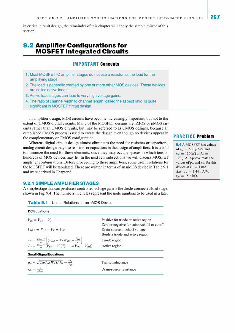
9.2.1 SIMPLE AMPLIFIER STAGESA simple stage that can produce a controlled voltage gain is the diode-connected load stage,
shown in Fig. 9.4. The numbers in circles represent the node numbers to be used in a later
Table 9.1 Useful Relations for an nMOS Device
DC Equations
V eff = V GS − V T Positive for triode or active region
Zero or negative for subthreshold or cutoff
V DSP
=V GS
−V T
=V eff Drain-source pinchoff voltage
Borders triode and active region
I D = µC oxW
L
(V G S − V T )V DS − V 2 DS
2
Triode region
I D = µC oxW
2 L[V GS − V T ]
2[1+ λ(V DS − V eff )] Active region
Small-Signal Equations
g m =
2µC ox(W / L) I D = 2 I DV eff
Transconductance
rds = 1λ I DP
Drain-source resistance
5/14/2018 0471410160-1 - slidepdf.com
http://slidepdf.com/reader/full/0471410160-1 6/30
26 8 C H A P T E R 9 I N T E G R A T E D C I R C U I T D E S I G N W I T H T H E M O S F E T
V DD
M2 2/1
M1 72/1
V 1
V 2
G1 D1, S2
S1, D2, G2
(a)
(b)
vin
vout
3
4
2
1
vin
gm1vgs1 gm2vgs2
gs2vs2
rds1 rds2 vout
Figure 9.4
(a) An ampli fi er with a
diode-connected load.
(b) Equivalent circuit.
simulation. This amplifier configuration demonstrates several important points relatin
general MOSFET IC amplifier design. The transconductance term, g s2, accounts for
body effect as the source to body voltage changes in device M 2.
The amplifier can be treated as a gain stage, M 1, driving a load impedance where
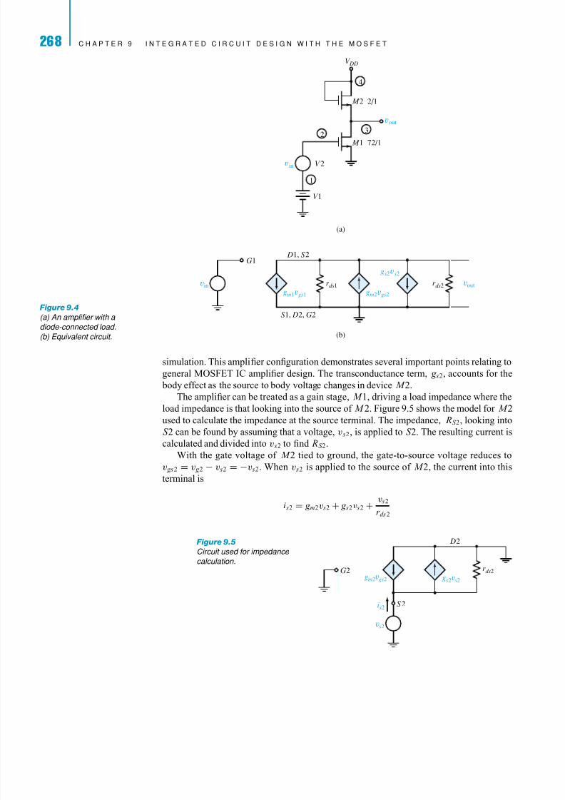
load impedance is that looking into the source of M 2. Figure 9.5 shows the model for
used to calculate the impedance at the source terminal. The impedance, RS 2, looking S 2 can be found by assuming that a voltage, v s2, is applied to S 2. The resulting curren
calculated and divided into v s2 to find RS 2.
With the gate voltage of M 2 tied to ground, the gate-to-source voltage reduce
v gs2 = v g 2 − v s2 = −v s2. When v s2 is applied to the source of M 2, the current into
terminal is
i s2 = g m2v s2 + g s2v s2 +v s2
rds 2
vs2
gm2vgs2
G2
D2
S2
gs2vs2
rds2
is2
Figure 9.5
Circuit used for impedance
calculation.
5/14/2018 0471410160-1 - slidepdf.com
http://slidepdf.com/reader/full/0471410160-1 7/30
S E C T I O N 9 . 2 A M P L I F I E R C O N F I G U R A T I O N S F O R M O S F E T I N T E G R A T E D C I R C U I T S
The impedance looking into this terminal is then
RS 2 =v s2
i s2
= 1
g m2 + g s2 + g ds 2
(9.6)
where g ds 2 = 1/rds 2.
The midband voltage gain is found by recognizing that device M 1 sees this load in
parallel with its own output impedance, rds 1. This parallel resistance is the output resistance, Rout, which can be expressed as
Rout = rds 1 RS 2 =1
g m2 + g s2 + g ds 2 + g ds 1
(9.7)
The midband voltage gain is then
A M B = − g m1 Rout = − g m1
g m2 + g s2 + g ds 2 + g ds 1
(9.8)
Typically, the largest term in the denominator will be g m2, which allows the gain to be
approximated by
A M B ≈ − g m1
g m2
(9.9)
For example, a 1-µ device ( L = 1µ) may have values of g m = 0.2 mA/V, g s =0.022 mA/V, and g ds = 0.001 mA/V, which leads to a 12% error in the approximation of
Eq. (9.9).
Examination of Eq. (9.9) shows that, for higher gains, g m1 must be much larger than
g m2, which can be accomplished by controlling the aspect ratios ( W / L) of the two devices.
The approximate variation of gain with device scaling can be derived from a consideration
of the equation for transconductance in the active region. This equation is found from
Table 9.1 and is
g m = 2µnC ox(W / L) I D (9.10)
Since the drain currents of both devices are equal, the voltage gain approximation of
Eq. (9.9) can now be written as
A M B ≈ −
2µnC ox(W 1/ L1) I D2µnC ox(W 2/ L2) I D
= −
(W 1/ L 1)
(W 2/ L 2)
1/2
(9.11)
It can be seen from Eq. (9.11) that the magnitude of the voltage gain varies as the
square root of the ratio of aspect ratios. If a gain of −6 is required, both devices can have
the same channel length with device M 1 using a channel width that is 36 times that of M 2.
We recognize that the actual gain may be slightly lower than the value indicated by
Eq. (9.11), but the approximation is suf ficient to begin a design that can be “tweaked ”
during simulation.
One consideration that becomes more important as power-supply voltages are lowered
in value is that of headroom. This term is used to indicate how much of the output voltage
swing cannot be used if serious distortion is to be avoided. If a stage that uses a 5-V dc
power supply has a headroom of 1.2 V, then the maximum usable output voltage range is
5− 1.2 = 3.8 V. For the circuit of Fig. 9.4, the output can be driven to within a few tenths
of a volt of ground by a positive input signal. The drain voltage can swing to its pinchoff

5/14/2018 0471410160-1 - slidepdf.com
http://slidepdf.com/reader/full/0471410160-1 8/30
27 0 C H A P T E R 9 I N T E G R A T E D C I R C U I T D E S I G N W I T H T H E M O S F E T
Rg
Cgs1(a)
Cgd 1G1 D1
S1
vin
vout
gm1vgs1
rds1 Rs2 C LCgs2Csb2Cdb1
Rg
Cin(b)
G1 D1
S1
vin
gm1vgs1
Rout Cout C L Figure 9.6
(a) High-frequency model of
diode-connected load stage.
(b) Simpli fi ed high-frequency
model.
value, which is V G S 1 − V T n = V eff1. This value is often near 200 – 300 mV. When the ou
swings positive, the load device must continue to conduct current; thus the gate-to-sou
voltage must equal or exceed the threshold voltage plus the effective voltage. The headrofor this stage is then a few tenths of a volt, perhaps 0.3 V, plus the threshold voltage of M
This headroom voltage is approximately V G S 1.
The upper corner frequency of an amplifier stage is often significant, but depe
on generator resistance and load capacitance as well as on the stage itself. Figure 9.
shows the high-frequency model for this stage including a load capacitance and a gener
resistance. Capacitor C gd is gate-to-drain capacitance, C gs is gate-to-source capacitance,
is drain-to-bulk capacitance, and C sb is the source-to-bulk capacitance. The capacitance C
bridgestheinputandoutputnodesandcanbere flected to theinput andoutputterminals u
the Miller effect. The input capacitance of Fig. 9.6(b) is C in = C gs1 + (1+ | A M B |)C
and the output capacitance is C out = C gd 1 + C db1 + C sb2 + C gs2.
From Eq. (9.7), the output resistance seen by the output capacitance is
Rout =1
g m2 + g ds 1 + g s2 + g ds 2
≈ 1
g m2 + g s2
(9
The amplifying stage has two upper corner frequencies; one caused by the input cir
and one caused by the output circuit. These frequencies are calculated by
f in−high =1
2π R g C in
(9
f out−high =1
2π Rout(C out + C L )(9
Depending on circuit values, these frequencies may be widely or narrowly separated
widely separated — for example, if the higher one is at least 5 times the lower frequenc
then the lower frequency approximates the overall upper corner frequency, f 2o. If the
frequencies are less than a factor of five different, the method of Chapter 3 must be use
calculate the overall upper corner frequency.
The circuit of Fig. 9.4, implemented on a 0.5-µ process, but with gate lengths of 1 µ
simulated by PSpice c to demonstrate several of the points made in this section. The Sp
netlist file is shown in Table 9.2. A 5-V power supply is used.

5/14/2018 0471410160-1 - slidepdf.com
http://slidepdf.com/reader/full/0471410160-1 9/30
S E C T I O N 9 . 2 A M P L I F I E R C O N F I G U R A T I O N S F O R M O S F E T I N T E G R A T E D C I R C U I T S
Table 9.2 Spice Netlist File for Amplifier with Diode-Connected Load
CH9.CIR
V11 0 1.0V
V22 1 AC0.005V
V3 4 0 5V
M13 2 0 0 N L=1UW=72U AD=360P AS=360P PD=82UPS=82U
M24 4 3 0 N L=1UW=2UAD=10PAS=10PPD=12UPS=12U
.AC DEC 10100 1000MEG
.OP
.PROBE
.LIB C5X.LIB
.END
This program uses a model for the MOSFETs named C5X.LIB.
P R A C T I C A L Considerations
In specifying a MOSFET device for analysis by Spice, the length and width of the
channel are first specified. The surface area of the drain and source follow, then the
external perimeters of the drain and source are specified. For device M 1, the channel
length in microns is 1 and the width is 72. The area of the drain is determined by
W 1 and the layout length of the drain region. For this device, the width is 72; thus
the length of the drain region must be 5 to result in an area of 72 × 5 = 360 square
microns. The perimeter used for the drain is not equal to 2W 1 + 2L D . Rather it is the
perimeter of the drain regionminus thewidth of thechannel: PD = W 1 + 2L D = 72+10 = 82. Certain capacitances are based on the external perimeter of the associated
region, but the capacitance associated with the side of the region that abuts the
channel is accounted for in a separate calculation. The same considerations apply
to the source terminal also.
The circuit is first simulated with neither source resistance nor load capacitance. The
results of this simulation are A M Bsim = −7.15 V/V, f 2o−sim = 202.1 MHz, with a headroom
of about 2.5 V. The headroom is found by doing a dc scan of the input voltage and watching
the output voltage for departures from linearity.
From calculation the midband voltage gain is found to be
| A M B | ≈
(W 1/ L1)
(W 2/ L2)
1/2
=√
36 = 6 V/V
The capacitance values given by the Spice simulation are
C in = C gs 1 + (1 + | A M B |)C gd 1 = 168 + (1+ 6)21.6 = 319.2 f F
and
C out = C gd 1 + C db 1 + C sb2 + C gs2 = 21.6 + 141 + 7.5 + 5 = 175.1 f F
The output resistance, calculated from Eq. (9.12) using parameters from the simulation,
is Rout = 4.35 k . The upper corner frequency with no source resistance and no load

5/14/2018 0471410160-1 - slidepdf.com
http://slidepdf.com/reader/full/0471410160-1 10/30
27 2 C H A P T E R 9 I N T E G R A T E D C I R C U I T D E S I G N W I T H T H E M O S F E T
Table 9.3 Summary of Simulation Results
for the Diode-Connected Load Stage
AMB sim =−7.15 V/V
C L, pF R g , kΩ f 2o −sim, MHz
0 0 202
1 0 30.10 339 1.52
1 339 1.48
capacitance is then
f 2o =1
2π RoutC out
= 1
2π × 4350 × 175.1 × 10−15= 209 MHz
When a load capacitance of 1 pF is added across the output terminals, the simu
tion shows an upper corner frequency of 30 MHz, and the calculation leads to a value
31.1 MHz.
If a rather large signal generator resistance of 339 k , which will also be used
succeeding circuits for comparison purposes, is added to the circuit along with the 1
output capacitance, the simulated value of upper corner frequency is 1.48 MHz. The up
corner frequency is lowered from 30 MHz to 1.48 MHz, due to the generator resistance
input capacitance. The overall upper corner frequency must then be caused primarily by
input circuit; thus, we calculate a value of
f 2o =1
2π R g C in
= 1
2π × 339 × 103 × 319.2 × 10−15= 1.47 MHz
If a generator resistance that equals the output resistance of this stage is used — tha
R g = 4.35 k — the upper corner frequency is 83.7 MHz without C L and 26.1 MHz w
C L = 1 pF added. Table 9.3 summarizes these results for the diode-connected load stag
P R A C T I C A L Considerations
Several practical points relating to IC design can be based on this analysis.
1. Although the load is not a resistor, the same techniques used in the analysis o
discrete circuits are still valid. The equivalent resistance of the MOSFET load is
first found and substituted for the load resistance.
2. The aspect ratio is important in determining the performance of the circuit. Very
large aspect ratios often result in analog design, while high-frequency digital
circuits generally keep this ratio at a low value to minimize capacitance and
required real estate or chip volume. Schematics of analog MOSFET circuits lab
the width and length of each device near the device, as shown in Fig. 9.4.3. Approximate results are useful to provide a starting point for circuit simulations
that are a necessity before an IC chip is laid out. Fabrication runs are very
expensive and mistakes must be avoided to minimize cost. Thus, the simulatio
step is never omitted in the IC design process. This step will use parameters fo
the MOS devices that are based on the actual process to be used in fabrication
4. Headroom may be an important consideration, since IC chips often use
low-voltage dc supplies.

5/14/2018 0471410160-1 - slidepdf.com
http://slidepdf.com/reader/full/0471410160-1 11/30
S E C T I O N 9 . 2 A M P L I F I E R C O N F I G U R A T I O N S F O R M O S F E T I N T E G R A T E D C I R C U I T S
There are some disadvantages to the stage discussed in this section that limit its use-
fulness. Larger channel areas lead to increased capacitance, so the bandwidth of high-gain
stages will be less than that of lower-gain stages for the diode-connected load stage. On
the other hand, it is a simple stage that has a low output impedance and is, therefore, not
affected to a great extent by load capacitance.
In the following chapter we will see that the BJT never uses the configuration of Fig. 9.4,
since the impedance looking into the emitter is re. This load impedance is too low to achieve
a significant voltage gain. We will also see that the load impedance cannot be increased
by scaling the areas of a BJT, since re is not a function of area. This difference is very
significant in BJT design and MOSFET design, the latter of which uses aspect ratio as a
critical design parameter.
V DD
M
M
vin
V G1
Figure 9.7
A diode-connected pMO
load.
The load device of Fig. 9.4 can be replaced by a pMOS device, as shown in Fig. 9.7.
This configuration eliminates the body effect of the load device and increases the resistance
due to a smaller value of µ p compared to µn. The value of µn is about three times that of
µ p. The approximation of Eq. (9.9) becomes more accurate, and the voltage gain can be
written as
| A M B
| = µn C oxn(W 1/ L1)
µ pC ox p(W 2/ L 2)
1/2
≈ 3(W 1/ L1)
(W 2/ L 2)
1/2
(9.15)
To approximate the upper corner frequency of the diode-connected pMOS stage, the
capacitances of Fig. 9.8 are added. It is generally true that C ds C db , giving a total capac-
itance from output to ground of
C out = C db 1 + C gd 1 + C db 2 + C gs 2
The output resistance can be found as
Rout
=
1
g m2 +
g ds 2 +
g ds 1 ≈
1
g m2
It is left as an exercise for the reader to derive this expression for output impedance.
+V DD
M2
M1
vin
V G1
Cgs2
Cgd 1
Cdb2
Cdb1
vout
Figure 9.8
Parasitic capacitances
determining the upper 3-dB
frequency.

5/14/2018 0471410160-1 - slidepdf.com
http://slidepdf.com/reader/full/0471410160-1 12/30
27 4 C H A P T E R 9 I N T E G R A T E D C I R C U I T D E S I G N W I T H T H E M O S F E T
+V DD
R
M2 W
M1 W
W 3 / L3 M3
vin
v
V G1 Figure 9.9
A MOSFET stage with an active
current source load.
The upper corner frequency is then
f 2o =1
2π C out Rout
(9
This value is approximately
f 2o = g m2
2π (C db1 + C db2 + C gs2 + C gd 1)(9
In many cases, the load capacitance or input capacitance to the next stage will lower
from this value, as seen earlier in this section.
P R A C T I C E Problem
9.5 Two n-devices are used
in a diode-connected amplifier stage similar to
that of Fig. 9.4(a). If
L 1 = L2 = 0.6 µ, calculate
W 1/ W 2 for a midband
voltage gain of −4.3 V/V.
Ans: 18.5.
9.2.2 ACTIVE LOAD STAGEA stage used often in IC design is the active load stage. Typically, the active load is a cur
source, often based on the current mirror. A simple MOSFET active load stage appear
Fig. 9.9.
There is a compelling reason to use active load stages in IC design. The device that a
as the load for the amplifying stage can present a large incremental load while allow
a reasonable drain current to flow. This large incremental load leads to a high gain
the stage, while the dc current can lead to acceptable values of transconductance and b
current. If a fixed resistor with a large value were used to achieve high gain, the dc d
across this element would be prohibitive for normal bias currents.
P R A C T I C A L Considerations
A simple current mirror might provide 100 µA of current to an amplifying stage whpresenting 60 k of incremental resistance to the stage. If a simple 60-k resistan
replaced the current mirror, the same incremental resistance would prevail, but th
dc voltage drop across the resistor would be
V R = 0.1× 60 = 6 V
The dc power supply for many MOSFET IC amplifiers is 5 V or less; thus, using
simple resistor is out of the question.
5/14/2018 0471410160-1 - slidepdf.com
http://slidepdf.com/reader/full/0471410160-1 13/30
S E C T I O N 9 . 2 A M P L I F I E R C O N F I G U R A T I O N S F O R M O S F E T I N T E G R A T E D C I R C U I T S
The difference between an active load and a simple resistor becomes even more
apparent when a more complex current mirror is used to produce a resistive load of
several hundred kilohms or greater. The dc drop across a several hundred kilohm
resistor, conducting a typical bias current, might be over 100 V.
The pMOS current mirror of Fig. 9.9 provides bias current to the amplifying device,
M 1. This device also sees an incremental resistive load that equals
Rout = rds 1 rds 2 =1
g ds 1 + g ds 2
(9.18)
The midband voltage gain is now
A M B = − g m1 Rout (9.19)
Since the values of rds can be high for both devices, the voltage gain for a single stage can
also be reasonably high.
The output voltage can be driven positive to the point that M 2 reaches its pinchoff value
for V DS . This voltage may be V D D − V eff2 = V D D − 0.4 V. In the negative direction, the
output can be driven to the point that M 1 reaches pinchoff, which is equal to V eff1
=0.4 V.
The headroom is perhaps 0.6 – 0.8 V.
The output capacitance for the amplifier of Fig. 9.9 is
C out = C db 1 + C db 2 + C gd 1 + C gd 2
which gives an upper corner frequency of
f 2o =( g ds 1 + g ds 2)
2π (C db1 + C db2 + C gd 1 + C gd 2)(9.20)
Again, we emphasize that a load capacitance or input capacitance of a following stage will
lower this value.
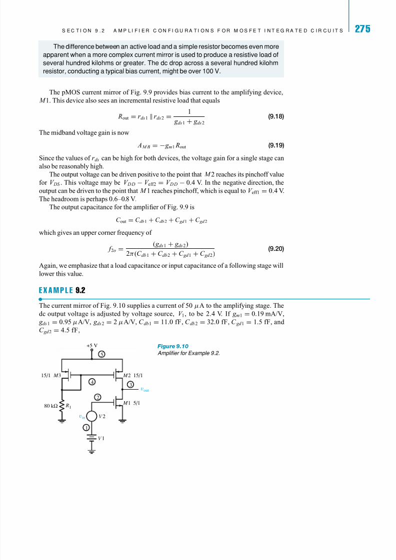
E X A M P L E 9.2 r
The current mirror of Fig. 9.10 supplies a current of 50 µA to the amplifying stage. The
dc output voltage is adjusted by voltage source, V 1, to be 2.4 V. If g m1 = 0.19 mA/V,
g ds 1 = 0.95 µA/V, g ds 2 = 2 µA/V, C db1 = 11.0 fF, C db2 = 32.0 fF, C gd 1 = 1.5 fF, and
C gd 2 = 4.5 fF,
+5 V
R1
M2 15/1
M1 5/1
V 2
V 1
15/1 M3
vin
v
out
80 kΩ
1
2
4
5
3
Figure 9.10
Ampli fi er for Example 9.2.

5/14/2018 0471410160-1 - slidepdf.com
http://slidepdf.com/reader/full/0471410160-1 14/30
27 6 C H A P T E R 9 I N T E G R A T E D C I R C U I T D E S I G N W I T H T H E M O S F E T
(a) Calculate the midband voltage gain, A M B .
(b) Calculate the upper corner frequency, f 2o.
(c) Verify results with a Spice simulation.
SOLUTION The output resistance for this stage is
Rout
=1
g ds 1 + g ds 2 =106
2.95 =339 k
Using Eq. (9.19) allows the voltage gain to be found as
A M B = − g m1 Rout = −0.19× 10−3 × 339 × 103 = −64.4 V/V
The output capacitance is
C out = C db1 + C db 2 + C gd 1 + C gd 2 = 11.0 + 32.0+ 1.5 + 4.5 = 49 fF
From Eq. (9.20), this gives an upper corner frequency of
f 2o =1
2π C out Rout
= 1
2π × 49 × 10−15 × 339 × 103= 9.58 MHz
The Spice netlist file is listed in Table 9.4. Corresponding node and element numb
are shown in Fig. 9.10.
Table 9.4 Spice Netlist File for Example 9.2
EX9-2.CIR
R1 0 4 80K
V11 0 1.275V
V22 1 AC0.005V
V3 5 0 5V
M13 2 0 0 N L=1UW=5UAD=25PAS=25PPD=15UPS=15U
M23 4 5 5 P L=1UW=15U AD=75PAS=75PPD=25UPS=25U
M34 4 5 5 P L=1UW=15U AD=75PAS=75PPD=25UPS=25U
.AC DEC 10100 10MEG
.OP
.PROBE
.LIB C5X.LIB
.END
The results of this simulation are A M Bsim = −63.6 V/V and f 2o−sim = 8.53 M
which compare well with the calculated results. A dc scan on the input voltage all
the active region of the output voltage to be evaluated. For this circuit, the active reg
extends from 0.4 V to 4.6 V, which also agrees well with theory.
Adding Generator Impedance and Load Impedance Only the ou
capacitance was used in developing Eq. (9.20) for upper corner frequency. As mentio
in connection with the diode-connected load stage, there are two other considerations
must be made for the practical circuit. One is the additional capacitance added betw
output and ground due to the input capacitance of the following stage or from the out
pad of an IC chip. The second is the generator resistance or output resistance of the prev
stage that drives the input capacitance of this stage. Both loops must be considered to re
in an accurate upper corner frequency.

5/14/2018 0471410160-1 - slidepdf.com
http://slidepdf.com/reader/full/0471410160-1 15/30
S E C T I O N 9 . 2 A M P L I F I E R C O N F I G U R A T I O N S F O R M O S F E T I N T E G R A T E D C I R C U I T S
Let us suppose that the output of the amplifier of Fig. 9.10 is brought to an output pad
and pin of an IC chip. The capacitance associated with the pad might exceed 1 pF. If the
simulation is repeated with a 1-pF load added, the upper corner frequency drops from 8.35
MHz to 431 kHz, a very large drop.
If this stage were loaded by a comparable stage rather than by 1 pF, the corner frequency
might drop by a factor of two rather than a factor of 20. In order to avoid this drop, a buffer
stage may be added to drive the 1-pF load without the large reduction in corner frequency.
Another possibility is to increase the values of W for all the devices. Although this increases
the capacitance, the output resistance decreases and g m increases to result in a comparable
voltage gain. The effect of the load capacitance on upper corner frequency will now be
much less.
As mentioned earlier, the stage of Fig. 9.10 is driven by a perfect voltage generator with
zero output resistance. If this stage were driven by an identical stage, the output impedance
of the first stage would become the generator resistance for the second stage. To demonstrate
the effect of generator resistance on upper corner frequency, a resistance of 339 k is used
as a generator resistance for the circuit of Fig. 9.10. This particular value of resistance will
be used in succeeding examples for comparison purposes. No external load capacitance is
used in this simulation. The simulated upper corner frequency is lowered in this situation
from a value of 8.35 MHz to 3.08 MHz.
This value can be calculated by noting that the input circuit will now cause a corner
frequency determined by the generator resistance and the input capacitance. The input
capacitance equalsthe sumof C gs1, C gb1, andthe Millereffect capacitance (1+ | A M B|)C gd 1.
From the output file of the simulation, these values are
| A M B | = 63.6 V/V C gs 1 = 13.35 fF C gd 1 = 1.5 f F C gb1 = 0.3 f F
The total input capacitance resulting is approximately 111 fF. With a value of R g =339k for generator resistance, this adds a corner frequency of
f in−high =1
2π C in R g
= 4.23 MHz
The amplifier now has an input corner frequency of 4.23 MHz and an output corner
frequency of 8.53 MHz. We use the method of Chapter 3 to calculate the overall upper
corner frequency when two single-pole upper corner frequencies make up the amplifier
response. The result is a calculated overall corner frequency of f 2o−calc = 3.56 MHz. This
value exceeds the simulated value of 3.08 MHz by 15%.
If a generator resistance of 339 k and a 1-pF load capacitance are both added to
the amplifier, the new upper corner frequency is found from simulation to be 399 kHz.
Table 9.5 summarizes the results of this simulation.
The active current source load provides a method to achieve high midband voltage
gains without the large discrepancy in size required by the diode-connected load amplifier.
Table 9.5 Summary of Simulation Results
for the Current-Source Load Stage
AMB sim = −63.6 V/V
C L, pF R g , kΩ f 2o −sim, MHz
0 0 8.53
1 0 0.43
0 339 3.08
1 339 0.40

5/14/2018 0471410160-1 - slidepdf.com
http://slidepdf.com/reader/full/0471410160-1 16/30
27 8 C H A P T E R 9 I N T E G R A T E D C I R C U I T D E S I G N W I T H T H E M O S F E T
It suffers from poor frequency response when a large capacitive load, much larger than
output capacitance of the stage, is present.
We can note that the midband voltage gain given by Eq. (9.19) will be increased if
is increased. This resistance can be increased by using a more complex current mirro
make the output resistance much larger than the output resistance of the amplifying sta
While this increases the midband voltage gain, the upper corner frequency due to the ou
loop, calculated from Eq. (9.20), decreases by the same factor. If this corner frequency is
dominant one, midband voltage gain and bandwidth can be exchanged directly by vary
the output resistance of the current mirror.
P R A C T I C A L Considerations
Although the upper corner frequency of the active load stage is significantly affect
by a 1-pF capacitance, it is possible to minimize this problem. The channel wid
of the output stage can be increased considerably to result in an increase in outp
capacitance and a corresponding decrease in output resistance. The upper corn
frequency with no external load can be approximately equal to that of the small
device. However, when a 1-pF load capacitance is added, the percentage increas
of capacitance is much less for the large device than for the small device. The effeon upper corner frequency is then much less for the larger device.
The effect of channel width, W , on the voltage gain can be seen in the following exam
E X A M P L E 9.3 r
In the circuit of Fig. 9.11, the current source generates 100 µA of current and has
incremental output resistance of rcs = 100 k . The device M 1 is a 1 = µ gate len
device with µC ox = 0.06 mA/V2 and λ = 0.03 V−1. Find the channel width to result
midband voltage gain of 100 V/V.
V DD
I
vin
vout
V 1
Figure 9.11
Circuit for Example 9.3.
SOLUTION The midband voltage gain of this stage is
A M B = − g m Rout
where
Rout = rcs rds 1
The value of rds 1 can be approximated by assuming that the drain pinchoff curren
approximately equal to 100 µA. The result is
rds 1
=1
λ I D =1
0.03 × 0.1 =333 k
Using the 100-k impedance of the current source, the output resistance is found to
Rout = 100 333 = 76.9 k
Recalling that
g m =
2µC ox(W / L) I D

5/14/2018 0471410160-1 - slidepdf.com
http://slidepdf.com/reader/full/0471410160-1 17/30
S E C T I O N 9 . 2 A M P L I F I E R C O N F I G U R A T I O N S F O R M O S F E T I N T E G R A T E D C I R C U I T S
we can write the magnitude of the voltage gain as
| A M B | = g m Rout =
2× 0.06 × (W / L)× 0.1 × 76.9 = 100 V/V
Solving this equation for the ratio of W / L leads to a value of 141 µ for W .
9.2.3 SOURCE FOLLOWER WITH ACTIVE LOADThe source follower provides a buffer stage, but the midband voltage gain is low, even less
than the value of unity approached by the BJTemitter-follower stage. The bandwidth is quite
high for both the emitter-follower and the source-follower stages. Figure 9.12 demonstrates
a source follower with a current mirror load.
P R A C T I C E Prob
9.6 Work Example 9
generator resistance o
R g = 50 k .
9.7 Work Example 9
generator resistance o
R g = 50 k and an i
capacitance to a follo
stage of C in2 = 100 f
9.8 The drain currencurrent mirror output
of Fig. 9.10 is increas
100 µA. Assuming th
capacitances remain
constant, calculate th
midband voltage gain
upper corner frequen
the amplifier.
Ans: A M B = −45.4 V
f 2o = 19.2 MHz.
9.9 Work Example 9
midband voltage gain
180 V/V is required.
Ans: W = 457 µ.
The device M 2 presents a resistance of rds 2 between the source of M 1 and ground.
In addition, device M 1 presents a resistance of rds 1 in parallel with 1/ g s1 to the dc power
supply, which is also ground for incremental signals. Again we note that the body effect in
M 1 must be included, since the source-to-substrate voltage of this device varies with the
output signal. In fact, it equals the output signal.
The circuit of Fig. 9.12(b) is redrawn in Fig. 9.13 and the pertinent parasitic capacitances
are added. The current source strength, g m1v gs1, can be written as g m1(vin − vout). In the
equivalent circuit, this current can be generated by two separate sources, as shown in
Fig. 9.13. The source terminal now appears at the top of the figure while the drain terminal
is grounded.
The two current sources g m1vout and g s1vout can be converted to conductances g m1 and
g s1, respectively. As a voltage appears at S 1, the currents through these conductances equal
the values that would be generated by the sources. Figure 9.14 shows an alternate equivalent
circuit that is used to find the voltage gain as a function of frequency. This circuit results from
taking a Thevenin equivalent of the current source, g m1vin, and the parallel resistance, Rout.
The circuit of Fig. 9.14 is analyzed to find that
A( j ω) = g m1 Rout1+ j ωC gs1/ g m1
1+ j ω(C gs1 + C out) Rout
(9.21)
+V DD
M3 M2
M1
G1
(b)(a)
D1
S1, D2
vin
v
out
vout
V 1
R
4
1
2
5
3
vinrds2
rds1gm1vgs1 gs1vs1
Figure 9.12
(a) A source-follower st
with current source load
(b) Equivalent circuit.

5/14/2018 0471410160-1 - slidepdf.com
http://slidepdf.com/reader/full/0471410160-1 18/30
28 0 C H A P T E R 9 I N T E G R A T E D C I R C U I T D E S I G N W I T H T H E M O S F E T
(a)
Cgs1G1
D1
S1
vin vou
gm1vin gm1vout gs1vout
rds1 rds2 Cout
(b)
Cgs1G1
D1
S1
vin vou
gm1vin
rds2rds1 Coutgs1
1gm1
1 Figure 9.13
(a) The high-frequency source
follower equivalent circuit.
(b) Using transconductances
for two current sources.
where
Rout =
1
g m1 + g s1 + g ds 1 + g ds 2
(9
and
C out = C sb1 + C db2 + C gd 2 ≈ C sb1 + C db2 (9
The midband gain can be evaluated from Eqs. (9.21) and (9.22) to be
A M B = g m1
g m1 + g s1 + g ds 1 + g ds 2
(9
In many submicron processes, the value of the denominator of Eq. (9.24) might eq
1.15 to 1.2 times g m1. This leads to values of midband gain ranging from about 0.
0.9 V/V.
The transfer function for voltage gain as a function of frequency shows a zero at
f zero = g m1
2πC gs1
(9
and a pole at
f pole = g m1 + g s1 + g ds 1 + g ds 2
2π (C gs1 + C out)(9
Typically, the zero frequency is higher than the pole frequency, and the asympt
frequency response appears as in Fig. 9.15. At high frequencies the capacitor C gs1 fe
+
— gm1vin Rout
RoutCoutvin
Cgs1 Figure 9.14
Alternate equivalent circuit of the source follower.
5/14/2018 0471410160-1 - slidepdf.com
http://slidepdf.com/reader/full/0471410160-1 19/30
S E C T I O N 9 . 2 A M P L I F I E R C O N F I G U R A T I O N S F O R M O S F E T I N T E G R A T E D C I R C U I T S
f pole f zero
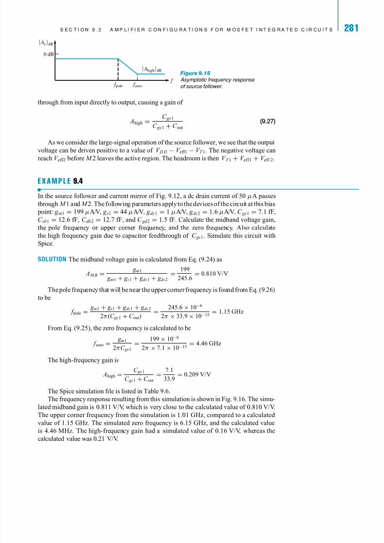
0 dB
f
AvdB
AhighdB Figure 9.15
Asymptotic frequency response
of source follower.
through from input directly to output, causing a gain of
Ahigh =C gs1
C gs1 + C out
(9.27)
As we consider the large-signal operation of the source follower, we see that the output
voltage can be driven positive to a value of V D D − V eff1 − V T 1. The negative voltage can
reach V eff2 before M 2 leaves the active region. The headroom is then V T 1 + V eff1 + V eff 2.
E X A M P L E 9.4 r
In the source follower and current mirror of Fig. 9.12, a dc drain current of 50 µA passes
through M 1and M 2. The following parameters apply to the devices of the circuit at this bias
point: g m1 = 199 µA/V, g s1 = 44 µA/V, g ds 1 = 1 µA/V, g ds 2 = 1.6 µA/V, C gs1 = 7.1 fF,
C sb1 = 12.6 fF, C db2 = 12.7 fF, and C gd 2 = 1.5 fF. Calculate the midband voltage gain,
the pole frequency or upper corner frequency, and the zero frequency. Also calculate
the high frequency gain due to capacitor feedthrough of C gs1. Simulate this circuit with
Spice.
SOLUTION The midband voltage gain is calculated from Eq. (9.24) as
A M B = g m1
g m1
+ g s1
+ g ds 1
+ g ds 2
= 199
245.6= 0.810 V/V
The pole frequency that will be near the upper corner frequency is found from Eq. (9.26)
to be
f pole = g m1 + g s1 + g ds 1 + g ds 2
2π (C gs 1 + C out)= 245.6 × 10⁻⁶
2π × 33.9× 10−15= 1.15 GHz
From Eq. (9.25), the zero frequency is calculated to be
f zero = g m1
2πC gs1
= 199 × 10−6
2π × 7.1 × 10−15= 4.46 GHz
The high-frequency gain is
Ahigh
=C gs 1
C gs1 + C out =7.1
33.9 =0.209 V/V
The Spice simulation file is listed in Table 9.6.
The frequency response resulting from this simulation is shown in Fig. 9.16. The simu-
lated midband gain is 0.811 V/V, which is very close to the calculated value of 0.810 V/V.
The upper corner frequency from the simulation is 1.01 GHz, compared to a calculated
value of 1.15 GHz. The simulated zero frequency is 6.15 GHz, and the calculated value
is 4.46 MHz. The high-frequency gain had a simulated value of 0.16 V/V, whereas the
calculated value was 0.21 V/V.
5/14/2018 0471410160-1 - slidepdf.com
http://slidepdf.com/reader/full/0471410160-1 20/30
28 2 C H A P T E R 9 I N T E G R A T E D C I R C U I T D E S I G N W I T H T H E M O S F E T
Table 9.6 Spice File for Example 9.4
EX9-4.CIR
R1 4 5 75K
V11 0 3.0V
V22 1 AC0.1V
V3 5 0 5V
M15 2 3 0 N L=1UW=5UAD=25PAS=25PPD=15UPS=15U
M23 4 0 0 N L=1UW=5UAD=25PAS=25PPD=15UPS=15U
M34 4 0 0 N L=1UW=5UAD=25PAS=25PPD=15UPS=15U
.AC DEC 10100 10000MEG
.OP
.PROBE
.LIB C5X.LIB
.END
A dc scan on the input voltage shows an output active region extending from appr
imately 0.32 to 3.03 V. The lower voltage is approximately V eff2, and the upper voltshould approximate V DD − V eff1 − V T 1.
1.15 6.15 f ,
AvdB
A= 0.811 V/V
Ahigh= 0.16 V/V
Figure 9.16
Simulated frequency response
for source follower.
We note that the upper corner frequencyfor the sourcefollower is 1.01 GHz, compare8.53 MHz for the comparable-sized current source load stage of Example 9.2. The prim
reason for this is the difference in the output resistance of the two stages. For the cur
source load stage, the output resistance is 339 k , and the source follower output resista
is about 4 k . In order to compare this stage when driven by a signal generator resistan
a 339-k resistance is inserted in the input lead. This simulation leads to an overall up
corner frequency of 101.5 MHz. The corresponding value for the current source loa
Example 9.2 is 3.08 MHz.
With a capacitive load of 1 pF and a generator resistance of 339 k , a Spice simula
shows an upper corner frequency of 37 MHz. Although this value is much lower than
unloaded value, it is considerably more than the corresponding frequency of the cur
source load stage, which was 399 kHz. Table 9.7 summarizes these results.
P R A C T I C A L Considerations
As noted earlier, capacitive loading can be a serious problem for an output stag
that connects to an IC pin, which will connect to the input of another circuit. Becau
of the high output resistance of configurations such as the active load stage, a sm
capacitance of a pF or less will decrease the upper corner frequency significant

5/14/2018 0471410160-1 - slidepdf.com
http://slidepdf.com/reader/full/0471410160-1 21/30
S E C T I O N 9 . 2 A M P L I F I E R C O N F I G U R A T I O N S F O R M O S F E T I N T E G R A T E D C I R C U I T S
Table 9.7 Summary of Simulation Results for
Source Follower
AMB sim = −0.811 V/V
C L, pF R g , kΩ f 2o −sim, MHz
0 0 1,010
1 0 36.60 339 101.6
1 339 37.2
The source follower stage is often inserted between a high-gain stage and the output
pin of a chip to serve as a buffer stage. This buffer presents a rather low capacitance
to the preceding stage, since there is no Miller multiplication of C gd and, as seen
from the simulation, a 1-pF load capacitance can result in a reasonably high upper
corner frequency.
9.2.4 THE CASCODE CONNECTIONThe cascode connection has been used for many years in high-frequency BJT circuits. It
has become more important in IC MOSFET design in recent years. We will discuss the
MOSFET cascode circuit in this section. Figure 9.17(a) shows the basic cascode circuit
with a current source load.
P R A C T I C E Prob
9.10 For the source
follower of Fig. 9.12,
the output resistance
looking into the sourc
terminal of M 1.
9.11 If g ds 1 and g ds 2
considered negligible
source follower of Ex
9.4, what will the mid
voltage gain be?
Ans: 0.819 V/V.
The equivalent circuit for the upper device would include a current generator of value
g m2V gs2. For this connection, v gs2 = −v s2; thus this current generator reverses the direc-
tion of current flow and removes the negative sign to lead to the value of g m2v s2, shown in
Fig. 9.17(b).
The resistance rcs is the output resistance of the current source. For a simple source, this
value would be rds . For a Wilson mirror, it would be considerably larger. The equivalent
circuit can be converted to a Thevenin circuit, as shown in Fig. 9.18. The output voltage is
vout = −ircs
where i is the incremental drain current. Note that the upper voltage source is proportional
to the source voltage of M 2, v s2. This voltage can be expressed as
v s2 = − g m1rds 1vin + irds 1
I D
M2V
(a)
M1
v
out
vin
G1
(b)
D2
D1, S2
S1
vout
vin
gm2vs2
gm1vin
gs2vs2rds2
rds1
rcs
vs2 —
Figure 9.17
(a) The MOSFET casco
ampli fi er stage. (b) The
equivalent circuit.

5/14/2018 0471410160-1 - slidepdf.com
http://slidepdf.com/reader/full/0471410160-1 22/30
28 4 C H A P T E R 9 I N T E G R A T E D C I R C U I T D E S I G N W I T H T H E M O S F E T
i
S1
D1, S2
D2
G1
vin
+
—
+
— (gm2 + gs2)rds2vs2
gm1rds1vin
vs2
rds2
rcs
Figure 9.18
An alternate equivalent circuit
for the cascode.
If the transconductance of M 2 is added to the body effect transconductance — that is,
g t 2 = g m2 + g s2
the midband voltage gain can be found to be
A M B = −( g m1rds 1
+ g t 2 g m1rds 1rds 2) rcs
rds 1 + rds 2 + rcs + g t 2rds 1rds 2 (9
This expression represents the product of two relatively large gains. As bias curr
decreases, the rds terms increase faster than the g m terms decrease. Gains of several thous
can be obtained with this circuit. However, as rds increases, the high-frequency respo
decreases, since the output resistance must drive the parasitic capacitance at the outpu
the stage.
A differential version of this stage is often used as an input stage in MOSFET op a
chips. A slightly different version of the cascode is the folded cascode that replaces M 2
a pMOS device with a drain connection to ground. We will not consider the folded casc
stage.
The headroom of the cascode circuit can be found to be
V headroom = V eff1 + V eff2 − V eff3 (9
The value of V eff3 will be negative for the pMOS device of a simple current mirror.
The upper corner frequency of the cascode can be found from the equivalent circ
shown in Fig. 9.19. The analysis of this circuit is somewhat complex. An accurate valu
the upper corner frequency can be found by simulation, but it can be approximated rat
easily from the equivalent circuit. We first note that with no signal generator resistance,
input capacitance will not influence the bandwidth. We next note that the corner freque
due to the capacitance C 1 will be affected by the parallel combination of rds 1 and
impedance looking into the source of M 2. This impedance will be much less than rds 1
can be approximated by
RS 2 =1
g m2 + g s2
vin Cin
G1 D2
D1, S2
S1
gm1vinrds1
C1 C2+
—
+ —
rds1 rds2vs2
(gm2 + gs2)vs2rds2rcs = rds3
vout
Figure 9.19
High-frequency model of the
cascode.

5/14/2018 0471410160-1 - slidepdf.com
http://slidepdf.com/reader/full/0471410160-1 23/30
S E C T I O N 9 . 2 A M P L I F I E R C O N F I G U R A T I O N S F O R M O S F E T I N T E G R A T E D C I R C U I T S
This corner frequency will be quite large, at least compared to that caused by C 2. If
the current source is a simple current mirror, its output impedance will be rcs = rds 3. The
resistance seen by C 2 is then rds 3 Rout2, where Rout2 is the impedance looking into the
drain of M 2. This latter impedance will be quite large since the source resistance of M 2
equals rds 1. This source resistance increases the output resistance of M 2 significantly; thus,
the resistance seen by C 2 is approximately rds 3. The upper corner frequency of the cascode
can then be approximated by
f 2o ≈1
2πrds 3C 2(9.30)
where C 2 = C db2 + C gd 2 + C db3 + C gd 3.
E X A M P L E 9.5 r
The cascode circuit of Fig. 9.20 has a dc drain current for all transistors of 50 µA. This
current is supplied by a simple current mirror with M 3 as the output device. With the bias
voltages shown, the parameters are g m1 = 181 µA/V, g m2 = 195 µA/V, g ds 1 = 5.87 µA/V,
g s2 = 57.1 µA/V, g ds 2 = 0.939 µA/V, g ds 3 = 3.76 µA/V, C db2 = 9.8 fF, C gd 2 = 1.5 fF,
C db3 = 40.9 fF, and C gd 3 = 4.5 f F, Calculate the midband voltage gain and the approximate
upper corner frequency of this cascode stage. Verify these results with a Spice simulation.
SOLUTION The midband gain is calculated from Eq. (9.28).
A M B = −( g m1rds 1 + g t 2 g m1rds 1rds 2) rds 3
rds 1 + rds 2 + rds 3 + g t 2rds 1rds 2
= −46.8 V/V
We note that this gain can be approximated by
A M B = − g m1rds 3 = −181
3.76= −48.1 V/V
Which assumes that the incremental current generated by device M 1, g m1vin, flows through
M 2 to develop the output voltage across rds 3.
This low value of voltage gain could be increased sharply by increasing the output
impedance of the current mirror to something much greater than rds 3.
+5 V
M3 15/1
M2 5/1
M1 5/1
15/1 M4
vout
V 1
72 kΩ
V 2
V 4
vin
2
4
1
6
7
5
3
Figure 9.20
Cascode circuit for Example
9.5.

5/14/2018 0471410160-1 - slidepdf.com
http://slidepdf.com/reader/full/0471410160-1 24/30
28 6 C H A P T E R 9 I N T E G R A T E D C I R C U I T D E S I G N W I T H T H E M O S F E T
The upper corner frequency is approximated by Eq. (9.30) as
f 2o =1
2πrds 3C 2= 1
2π × 56.7 × 10−15 × 266 × 103= 10.6 MHz
The Spice netlist is included in Table 9.8.
Table 9.8 Spice Netlist for Example 9.5
EX9-5.CIR
R1 0 4 72K
V11 0 2.1V
V22 6 AC0.005V
V3 5 0 5V
V42 0 1.3V
M17 6 0 0 N L=1UW=5UAD=25PAS=25PPD=15UPS=15U
M23 1 7 0 N L=1UW=5UAD=25PAS=25PPD=15UPS=15U
M33 4 5 5 P L=1UW=15U AD=75PAS=75PPD=25UPS=25U
M44 4 5 5 P L=1UW=15U AD=75PAS=75PPD=25UPS=25U
.AC DEC 10100 100MEG
.OP
.PROBE
.LIB C5X.LIB
.END
The results of the simulation are A M Bsim = −46.9 V/V and f 2o−sim = 9.65 MHz.
calculated gain is very close to the simulated value, and the upper corner frequenc
calculated to be about 10% higher than the simulated value.
In order to demonstrate the effect of current on gain and bandwidth, the dc drain curof the circuit is dropped from 50 µA to 10.7 µA. For this situation, the simulated res
are A M Bsim = −94.1 V/V and f 2o−sim = 2.52 MHz. The gain has approximately doub
while the bandwidth has dropped by a factor of about 4.
The effect on voltage gain can be seen from the approximation
A M B = − g m1rds 3
Since g m varies as the square root of drain current and rds varies approximately inver
with current, the voltage gain at a new current, I D2, compares to the voltage gain at a cur
of I D1 as
A M B ( I D2) = I D1
I D2 A M B ( I D1)
For this circuit, the new gain at 10.7 µA would be approximated as
A M B (10.7) =
50
10.7 A M B (50) = 2.16 × (−46.8) = −101 V/V
The bandwidth decrease is due to the increase in output resistance when drain curren
lowered.

5/14/2018 0471410160-1 - slidepdf.com
http://slidepdf.com/reader/full/0471410160-1 25/30
S E C T I O N 9 . 2 A M P L I F I E R C O N F I G U R A T I O N S F O R M O S F E T I N T E G R A T E D C I R C U I T S
Table 9.9 Summary of Simulation Results for
Cascode Amplifier
AMB sim = −46.9 V/V
C L, pF R g , kΩ f 2o −sim, MHz
0 0 9.65
1 0 0.550 339 8.95
1 339 0.55
If a signal generator resistance is present, a second corner frequency is added at the input
due to C in of Fig. 9.19. When a 339-k generator resistance is added to the simulation of
Table 9.8, the new upper corner frequency is 8.95 MHz. This value represents a relatively
small change from the original value of 9.65 MHz, which implies that C in is rather small.
Thus we see one of the advantages of the cascode connection; that is, the input capacitance
is small because the Miller effect is minimized by a small voltage gain from gate to drain
of M 1.
If a load capacitance of 1 pF is added but no generator resistance is present, the upper
corner frequency is lowered to 552 kHz. Adding the generator resistance to this circuit leads
to no further reduction of the upper corner frequency.
The headroom for the cascode circuit is simulated to be about 0.94 V. Using simulated
values of the effective voltages of Eq. (9.29) gives a calculated value of
V headroom = 0.47+ 0.45 + 0.41 = 1.33 V
These results are summarized in Table 9.9.
P R A C T I C E Prob
9.12 Rework Examp
if the current from th
mirror is changed to
9.2.5 THE ACTIVE CASCODE AMPLIFIERAn amplifier that behaves much like the cascode circuit, but offers slightly more headroom
and requires one less bias voltage source, is the active cascode stage of Fig. 9.21. It also
exhibits high gain although it has a lower bandwidth than the cascode stage with a current
mirror load. The only difference between this circuit and the cascode circuit is that the gates
of both nMOS amplifying stages, M 1 and M 2, are tied together and driven by the input
signal. The load is formed by the two pMOS devices, M 3 and M 4, which again connect
both gates together and also to a bias source. The connection of M 3 and M 4 is called a
partial cascode stage.
V
V BB
V GG
vin
Figure 9.21
An active cascode stag
a partial cascode load.
The partial cascode can be found to present an output impedance, looking into the drain
of M 4, of
Ro4 = rds 3 + rds 4 + g t 4rds 3rds 4 (9.31)
where g t 4 = g m4 + g s4.
The midband voltage gain is evaluated as
A M B = −
g m1
g ds 1
+ g m2
g ds 2
+ g m1 g t 2
g ds 1 g ds 2
Ro4
Ro4 + Ro2
(9.32)
where
Ro2 = rds 1 + rds 2 + g t 2rds 3rds 4 (9.33)
and g t 2 = g m2 + g s2.

5/14/2018 0471410160-1 - slidepdf.com
http://slidepdf.com/reader/full/0471410160-1 26/30
28 8 C H A P T E R 9 I N T E G R A T E D C I R C U I T D E S I G N W I T H T H E M O S F E T
The device M 2 is chosen to have a larger aspect ratio than that of M 1, and the sam
true of M 4 compared to M 3. Thus the outer devices, M 1 and M 3, are forced to operat
the triode region or near the edge of the triode and the active region.
The gain expression can be reduced by using aspect ratios of the pMOS devices that
three times the corresponding nMOS devices, which will result in the following approxim
transconductance relationships:
g t 2 = g t 4 g r ds 1 = g rd s3 g ds 2 = g ds 4
With some simple approximations, the voltage gain can be expressed as
A M B ≈ − g t 2 g m1
2 g ds 1 g ds 2
(9
The output impedance of the active cascode for comparable devices is considera
greater than that of the cascode. Of course, additional devices could be used in the curr
mirror load of the cascode to increase the output impedance. For a four-transistor circ
the active cascode has higher gain, smaller headroom, and fewer required bias voltages.
disadvantage is a smaller bandwidth.
The headroom is
V headroom = V eff1 + V eff3 (9
which may be 0.4 to 0.5 V.
A Spice netlist file of the active cascode with drain currents equal to about 50 µA
shown in Table 9.10.
The results of this simulation are indicated in Table 9.11.
Both the cascode and active cascode will show an increased gain and decreased ba
width as drain current decreases. For the circuits of Figs. 9.17(a) and 9.21, the drain curr
are decreased to approximately 10 µA. The new simulated results for the cascode cir
with no additional loading are A M Bsim = −70.9 V/V and f 2o−sim = 3.03 MHz. The res
for the active cascode are A M Bsim = −624 V/V and f 2o−sim = 63 kHz.
All of the stages discussed in this chapter require a voltage bias on the gate of
amplifying stage. Voltage reference circuits can be constructed to provide the necessvoltage bias; however, these sources will not be considered here.
Table 9.10 Spice Netlist File for Active Cascode Amplifier
ACTCAS.CIR
V11 0 1.333V
V2 5 0 5V
V34 1 AC0.001V
V47 0 3.52V
M13 4 0 0 N L=1UW=5UAD=25PAS=25PPD=15UPS=15U
M22 4 3 0 N L=1UW=40U AD=200P AS=200P PD=50UPS=50U
M36 7 5 5 P L=1UW=15U AD=75PAS=75PPD=25UPS=25U
M42 7 6 5 P L=1UW=120UAD=600P AS=600P PD=130U PS=130U
.AC DEC 10100 100MEG
.OP
.PROBE
.LIB C5X.LIB
.END

5/14/2018 0471410160-1 - slidepdf.com
http://slidepdf.com/reader/full/0471410160-1 27/30
S E C T I O N 9 . 2 A M P L I F I E R C O N F I G U R A T I O N S F O R M O S F E T I N T E G R A T E D C I R C U I T S
Table 9.11 Summary of Results for Active
Cascode Amplifier
AMB sim =−291 V/V
C L, pF R g , kΩ f 2o −sim, kHz
0 0 249
1 0 69.50 339 87.2
1 339 45.9
D I S C U S S I O N O F D E M O N S T R A T I O N P R O B L E M
The amplifier of the Demonstration Problem is repeated here for convenience. The first part of
the problem consists of solving for the current through the 8-k resistance at the current mirror
input, which will allow the output current from M 2 to be equated to the current into M 1 with
an output voltage of 2.5 V.
5 V
8 kΩ
M2
M1
M3
vin
V DSQ1
vout
V 1
Ampli fi er for Demo
Problem
The drain current of M 3 can be written as
I D3 = K p[V GS 3 − V T p]2[1− λ(V DS 3 − V DSP3)]
We note that V GS 3 = V G3 − V D D = 8 I D3 − 5 V and V DS 3 − V DSP3 = V T p = −1 V. Writing the
right side of the drain current equation in terms of I D3 leads to a quadratic equation. The solution
of this equation results in I D3 = 0.2888 mA and V G3 = 2.31 V. The pinchoff current of both
M 2 and M 3 is
I D P = K p [V GS − V T p]2 = 0.1× [−1.69]2 = 0.2856 mA
The pinchoff voltage is V DSP = −1.69 V.
We now equate the current, I D2, to the current I D1, which allows the equation
I DSP2[1− λ(V DS 2 − V DSP2)] = I DSP1[1+ λ(V DS 1 − V DSP1)]
to be written. The left side of this equation is I DS 2 and the right side is I DS 1. Noting that

5/14/2018 0471410160-1 - slidepdf.com
http://slidepdf.com/reader/full/0471410160-1 28/30
29 0 C H A P T E R 9 I N T E G R A T E D C I R C U I T D E S I G N W I T H T H E M O S F E T
I DS 2 = 0.1[−1.69]2 leads to
I DS 2 = 0.1[−1.69]2[1− 0.01(−2.5 + 1.69)] = 0.2879 mA
This value is equated to the right side of the equation, which is
I DS 1 = 0.2879 = 0.12[V G S 1 − 1]2[1 + 0.01(1.035 − 0.01V GS 1)]
Solving for V GS 1 gives
V GS 1 = 2.54 V
When this voltage is applied to the gate of M 1, a current of 0.2879 mA and a voltage of
V DSQ1 = 2.5V result.
The incremental values of rds 1 and rds 2 can now be found from
rds = 1
λ I DSP
The values of rds 1 and rds 2 are equal and are both 350 k . The resistance between output and
ground is the parallel combination of these two resistances or 175 k .
The midband voltage gain is
A M B = − g m1 Rout
The value of g m is found to be
g m =
2µC ox(W / L) I D
For M 1, the transconductance is 0.37 mA/V, which gives a gain of
A M B = −0.37× 175 = −64.7 V/V
S U M M A R Y
The MOSFET amplifier designed for implementation as
an IC reduces to a minimum the number of resistors
required. Active loads often replace the resistors used in
discrete MOSFET amplifiers.
The current mirror is used extensively in IC design. It
serves as a bias current source as well as an active load.
The individual amplifier stage must not be analyzed as
an isolated stage. The driving source resistance that may
arise from a previous stage and the load capacitance tha
may arise from a following stage or an IC output pad
must be included in the analysis of frequency
response.
The source follower has a low voltage gain but a very g
frequency response.
The cascode and partial cascode connections provide ra
ef ficient amplifying configurations.

5/14/2018 0471410160-1 - slidepdf.com
http://slidepdf.com/reader/full/0471410160-1 29/30
P R O B L E M S
P R O B L E M S
S E C T I O N 9 . 1 M O S F E T C U R R E N T M I R R O R S
9.1 If µW C ox/2 L = 50 µA/V2, V T = 0.8 V, and λ = 0.02,
calculate the drain current in the circuit shown.
Figure P9.1
5 V
10 kΩ
9.2 For the circuit of Problem 9.1, calculate the value of
pinchoff current, I D P , and pinchoff voltage, V DSP .
9.3 If µW C ox/2 L = 80µA/V2, V T = −1.0 V, and λ = 0.02,
calculate the drain current in the circuit shown.
Figure P9.3
5 V
8 kΩ
9.4 For the circuit of Problem 9.3, calculate the value of pin-
choff current, I D P , and pinchoff voltage, V DSP .
9.5 If µW C ox/2 L = 50 µA/V2, V T = 0.8 V, and λ = 0.02,
calculate the ratio I o/ I in for the circuit of Fig. 9.1
when I in = 72 µA and V DS 2 = 6 V. Assume
MOSFETs.
9.6 In Fig. 9.1, thecurrent source, I in, isgenerated b
voltage source in series with a 60-k resistor. Mdevices are used, except for V T 2, with values as
Problem 9.5.
(a) Calculate the current, I in.
(b) Calculate V G S .
(c) If I o/ I in is to be unity when V DS 2 = 8 V, what
required value of V T 2?
(d) With the value of V T 2 in part (c), what is I o/ I in
V DS 2 = 16 V?
9.7 Derive the output impedance, looking into the d
the circuit shown. Express the result in terms of rds , RS . Neglect body effect for this derivation. Comp
impedance to that resulting when RS = 0.
Figure P9.7
vout
+V DD
RS
V 1
vin
Rout
S E C T I O N 9 . 2 . 1 S I M P L E A M P L I F I E R S T A G E S
9.8 What is the approximate midband voltage gain for the
circuit of Fig. 9.4(a) if the dimensions of M 1 are W 1 = 24 µ
and L1 = 1 µ and the dimensions of M 2 are W 2 = 6 µ and
L 2 = 2 µ?
9.9 What should the value of W 1 be in Fig. 9.4(a) to lead to amidband voltage gain of −42 V/V?The lengthof the channel
of M 1 is L1 = 1 µ, and the dimensions of M 2are W 2 = 2 µ
and L2 = 2 µ.
D 9.10 If the circuit of Fig. 9.4(a) is to have a midba
age gain of approximately −4.8 V/V, to what valu
W 1 be changed?
9.11 What is the upper corner frequency of the amp
Fig. 9.4(a) if C out = 98 fF, g m2 = 0.4 mA/V, an0.05 mA/V? Assume that the load capacit
50 fF.
S E C T I O N 9 . 2 . 2 A C T I V E L O A D S T A G E
9.12 In the active load stage of Fig. 9.10, the current from the
mirror is increased from 50 µA to 100 µA. What would you
now expect the midband voltage gain to be? Expl
calculations.

5/14/2018 0471410160-1 - slidepdf.com
http://slidepdf.com/reader/full/0471410160-1 30/30
29 2 C H A P T E R 9 I N T E G R A T E D C I R C U I T D E S I G N W I T H T H E M O S F E T
9.13 Rework the Demonstration Problem if all parame-
ters remain the same except λ p = 0.024 V−1 and λn =0.02 V−1.
9.14 Rework the Demonstration Problem if all parameters
remain the same except K n = 0.16 mA/V2.
9.15 In the circuit of Fig. 9.10, a resistance of value 400 k is
placed in series with the input signal generator. Calculate thevalue of load capacitance that causes the input upper corner
frequency to equal the output upper corner frequency. What
is the overall upper corner frequency? Use the capacitance
values from the circuit simulation.
9.16 In the circuit of Fig. 9.10, a resistance is placed in se-
ries with the input signal generator. Calculate the value of
this resistor to cause the input upper corner frequency to
equal the output upper corner frequency. Assume a zero
value for load capacitance. Use the capacitance values from
the circuit simulation. What is the overall upper corner
frequency?
D 9.17 In the circuit shown, the current source has infi-
nite impedance and can be adjusted to supply whatever cur-
rent is required to keep M 1 in the active region as V GS is
changed. If λ = 0.03 V−1, V T = 1.02 V, and µC oxW /2 L =0.2 mA/V2,
(a) Calculate A M B when V G S = 2 V.
(b) Find the value of V G S required to double this voltage
gain. Assume that V DS = 4 V for both cases.
Figure P9.17
vout
+V DD
V GS
vin
D 9.18 If the current source in Problem D9.17 is fixed
value of 100 µA, what must V GS be to result in V DS = 4
What is the value of A M B for this bias?
9.19Rework Example 9.3 for a required midband voltage
of −76 V/V.
9.20 In the circuit of Example 9.3, the drain current is low
to 50 µA. Approximate the new value of midband volt
gain. Explain this approximation.
D 9.21 Using devices with L = 1 µ, |V T | = 1 V , λ = 0
V−1, and µC ox = 0.06 mA/V2, design an active load st
with a simple current mirror load to have a midband g
of −120 V/V.
S E C T I O N 9 . 2 . 3 S O U R C E F O L L O W E R W I T H A C T I V E L O A D
9.22 Rework Example 9.4 if all parameters remain the same
except g m , which becomes g m1 = 300 mA/V.9.23 Find the overall upper corner frequency of the source
follower of Example 9.4 if a load capacitance of 0.6 pF is
added.
9.24 Find the overall upper corner frequency of the sou
follower of Example 9.4 if a load capacitance of 0.6 padded and a generator resistance of 100 k is present.
culate the midband voltage gain.
S E C T I O N 9 . 2 . 4 T H E C A S C O D E C O N N E C T I O N
9.25 In Example 9.5, using the cascode circuit of Fig. 9.20, the
current from the mirror is increased from 50 µA to 100 µA.
What would you now expect the midband voltage gai
be? Explain your calculations.
S E C T I O N 9 . 2 . 5 T H E A C T I V E C A S C O D E A M P L I F I E R
9.26 Explain why the midband voltage gain increases with
decreasing drain current in the active cascode amplifier.


![089 ' # '6& *#0 & 7 · 2018. 4. 1. · 1 1 ¢ 1 1 1 ï1 1 1 1 ¢ ¢ð1 1 ¢ 1 1 1 1 1 1 1ýzð1]þð1 1 1 1 1w ï 1 1 1w ð1 1w1 1 1 1 1 1 1 1 1 1 ¢1 1 1 1û](https://img.pdfslide.us/doc/110x75/60a360fa754ba45f27452969/089-6-0-7-2018-4-1-1-1-1-1-1-1-1-1-1-1-1-1.jpg)


![[XLS] · Web view1 1 1 2 3 1 1 2 2 1 1 1 1 1 1 2 1 1 1 1 1 1 2 1 1 1 1 2 2 3 5 1 1 1 1 34 1 1 1 1 1 1 1 1 1 1 240 2 1 1 1 1 1 2 1 3 1 1 2 1 2 5 1 1 1 1 8 1 1 2 1 1 1 1 2 2 1 1 1 1](https://img.pdfslide.us/doc/110x75/5ad1d2817f8b9a05208bfb6d/xls-view1-1-1-2-3-1-1-2-2-1-1-1-1-1-1-2-1-1-1-1-1-1-2-1-1-1-1-2-2-3-5-1-1-1-1.jpg)

![1 $SU VW (G +LWDFKL +HDOWKFDUH %XVLQHVV 8QLW 1 X ñ 1 … · 2020. 5. 26. · 1 1 1 1 1 x 1 1 , x _ y ] 1 1 1 1 1 1 ¢ 1 1 1 1 1 1 1 1 1 1 1 1 1 1 1 1 1 1 1 1 1 1 1 1 1 1 1 1 1 1](https://img.pdfslide.us/doc/110x75/5fbfc0fcc822f24c4706936b/1-su-vw-g-lwdfkl-hdowkfduh-xvlqhvv-8qlw-1-x-1-2020-5-26-1-1-1-1-1-x.jpg)


![1 1 1 1 1 1 1 ¢ 1 , ¢ 1 1 1 , 1 1 1 1 ¡ 1 1 1 1 · 1 1 1 1 1 ] ð 1 1 w ï 1 x v w ^ 1 1 x w [ ^ \ w _ [ 1. 1 1 1 1 1 1 1 1 1 1 1 1 1 1 1 1 1 1 1 1 1 1 1 1 1 1 1 ð 1 ] û w ü](https://img.pdfslide.us/doc/110x75/5f40ff1754b8c6159c151d05/1-1-1-1-1-1-1-1-1-1-1-1-1-1-1-1-1-1-1-1-1-1-1-1-1-1-w-1-x-v.jpg)