Embed Size (px)
Citation preview
03/14/2012
Error Patterns in MLC NAND Flash Memory:Measurement, Characterization, and AnalysisError Patterns in MLC NAND Flash Memory:
Measurement, Characterization, and AnalysisYu Cai1, Erich F. Haratsch2 , Onur Mutlu1 and Ken Mai1
1. DSSC, ECE Department, Carnegie Mellon University2. LSI Corporation
2
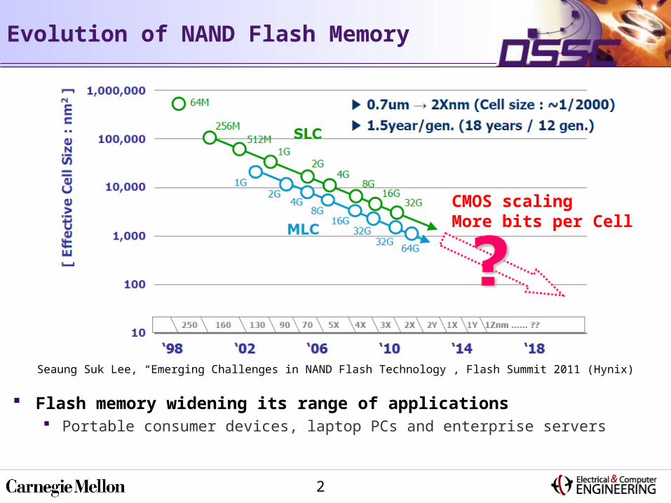
Evolution of NAND Flash Memory
Flash memory widening its range of applications Portable consumer devices, laptop PCs and enterprise servers
Seaung Suk Lee, “Emerging Challenges in NAND Flash Technology”, Flash Summit 2011 (Hynix)
CMOS scalingMore bits per Cell
3
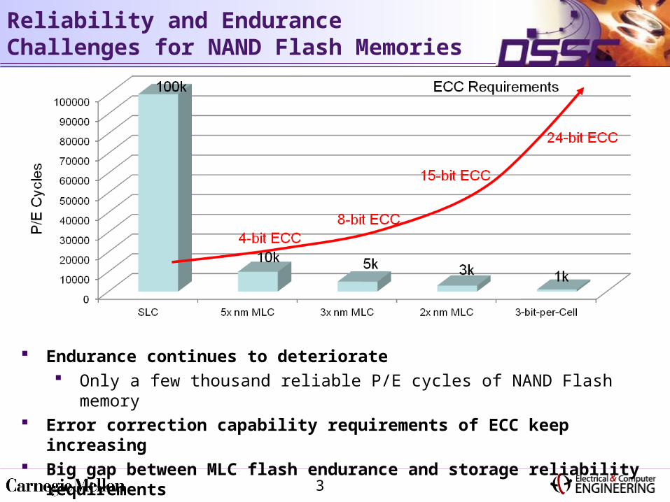
Reliability and Endurance Challenges for NAND Flash Memories
Endurance continues to deteriorate Only a few thousand reliable P/E cycles of NAND Flash memory
Error correction capability requirements of ECC keep increasing Big gap between MLC flash endurance and storage reliability requirements
Enterprise storage needs >50k P/E cycles
4
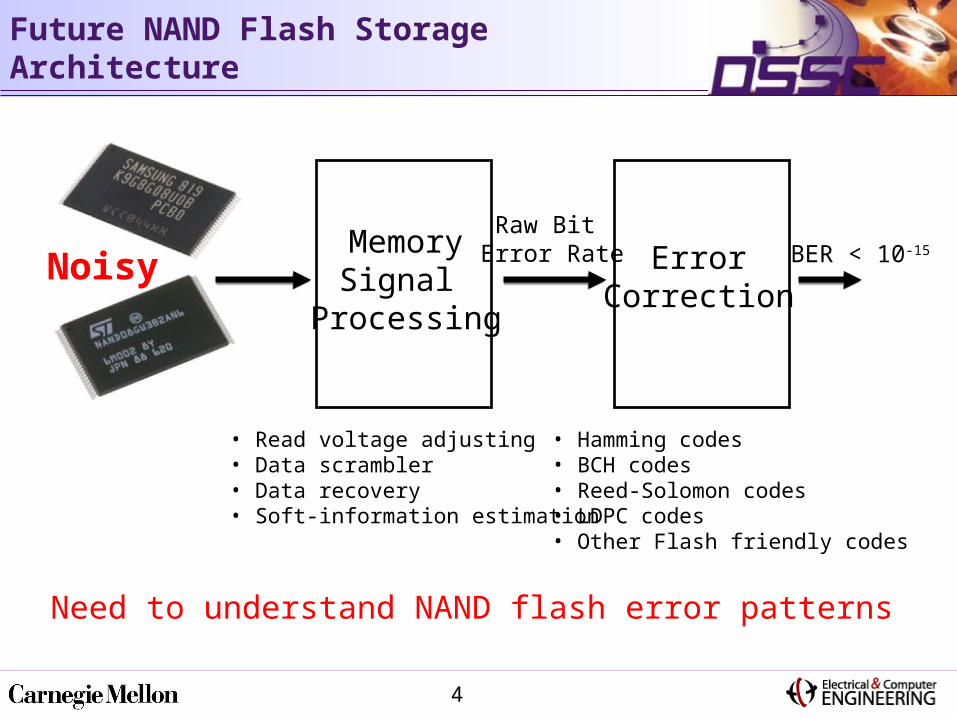
Future NAND Flash Storage Architecture
MemorySignal
Processing
ErrorCorrection
Raw Bit Error Rate
• Hamming codes• BCH codes • Reed-Solomon codes• LDPC codes• Other Flash friendly codes
BER < 10-15
Need to understand NAND flash error patterns
• Read voltage adjusting• Data scrambler• Data recovery• Soft-information estimation
Noisy
5
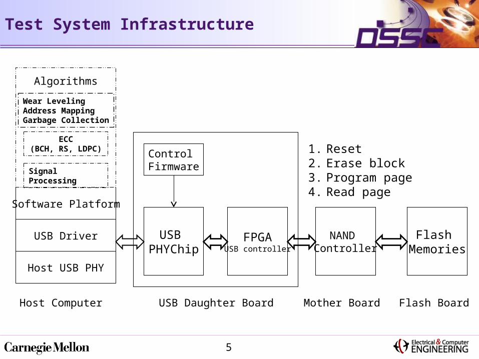
Test System Infrastructure
Host USB PHY
USB Driver
Software Platform
USB PHYChip
Control Firmware
FPGAUSB controller
NAND Controller
Signal Processing
Wear LevelingAddress MappingGarbage Collection
Algorithms
ECC(BCH, RS, LDPC)
Flash Memories
Host Computer USB Daughter Board Mother Board Flash Board
1. Reset2. Erase block3. Program page4. Read page
6
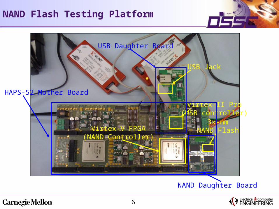
NAND Flash Testing Platform
USB Jack
Virtex-II Pro(USB controller)
Virtex-V FPGA(NAND Controller)
HAPS-52 Mother Board
USB Daughter Board
NAND Daughter Board
3x-nmNAND Flash
7
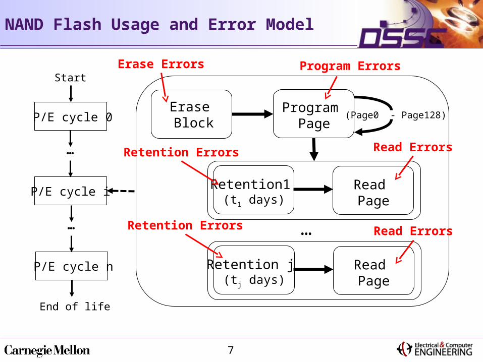
NAND Flash Usage and Error Model
…
(Page0 - Page128)Program
PageErase Block
Retention1 (t1 days)
Read Page
Retention j (tj days)
Read Page
P/E cycle 0
P/E cycle i
Start
…
P/E cycle n
…
End of life
Erase Errors Program Errors
Retention Errors Read Errors
Read ErrorsRetention Errors
8
Testing Methodology
Erase errors Count the number of cells that fail to be erased to “11” state
Program interference errors Compare the data immediately after page programming and the data
after the whole block being programmed
Read errors Continuously read a given block and compare the data between
consecutive read sequences
Retention errors Compare the data read before retention and after retention
Characterize short term retention errors under room temperature Characterize long term retention errors by baking in the oven under 125℃
9
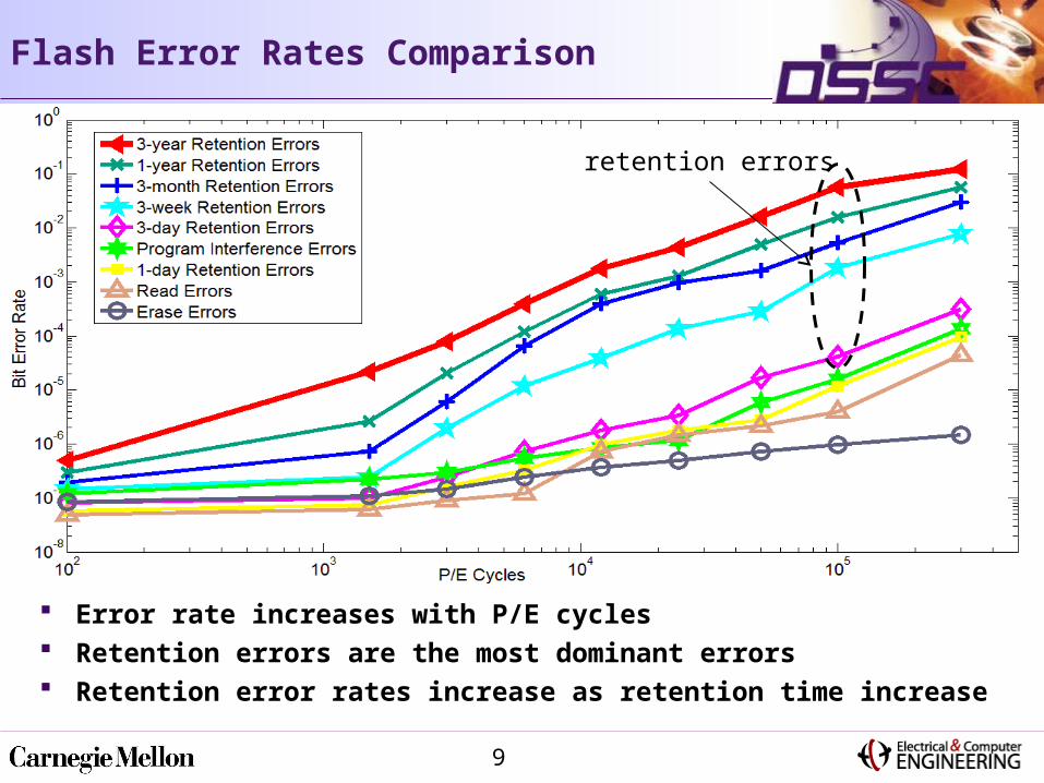
Flash Error Rates Comparison
Error rate increases with P/E cycles Retention errors are the most dominant errors Retention error rates increase as retention time increase
retention errors

10
Retention Error Mechanism
LSB/MSB
Electrons loss from the floating gate causes retention errors Cells with more programmed electrons suffer more from retention errors Threshold voltage is more likely to shift one interval than multiple intervals
11 10 01 00Vth
REF1 REF2 REF3
Erased Fully programmed
Stress Induced Leakage Current (SILC)
FloatingGate
11
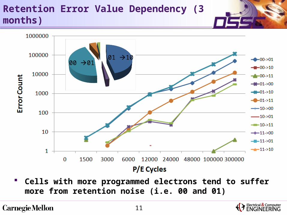
Retention Error Value Dependency (3 months)
00 0101 10
Cells with more programmed electrons tend to suffer more from retention noise (i.e. 00 and 01)
12
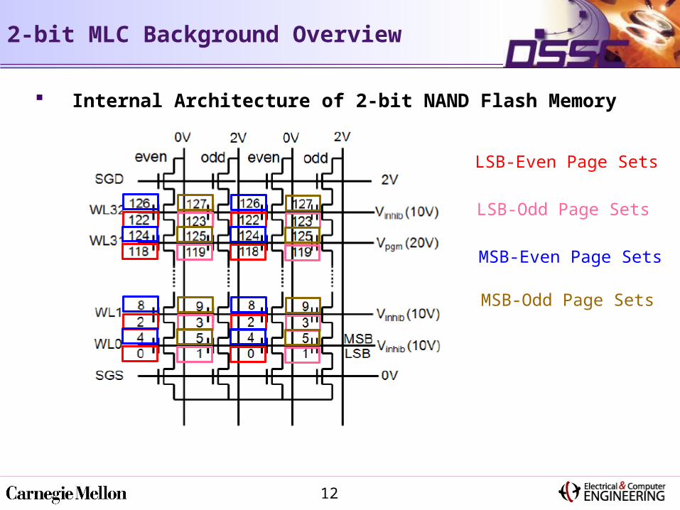
2-bit MLC Background Overview
Internal Architecture of 2-bit NAND Flash Memory
LSB-Even Page Sets
LSB-Odd Page Sets
MSB-Even Page Sets
MSB-Odd Page Sets
13
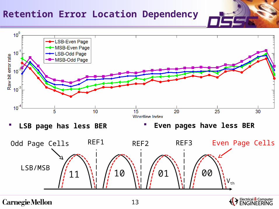
Retention Error Location Dependency
LSB page has less BER Even pages have less BER
Vth
11 10 01 00
REF1 REF2 REF3Odd Page Cells Even Page Cells
LSB/MSB
14
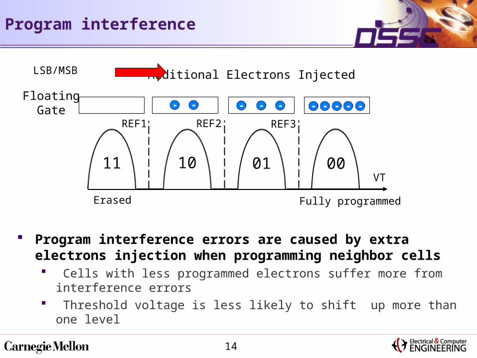
Program interference
LSB/MSB
Program interference errors are caused by extra electrons injection when programming neighbor cells Cells with less programmed electrons suffer more from interference errors Threshold voltage is less likely to shift up more than one level
11 10 01 00VT
REF1 REF2 REF3
Erased Fully programmed
FloatingGate
Additional Electrons Injected
15
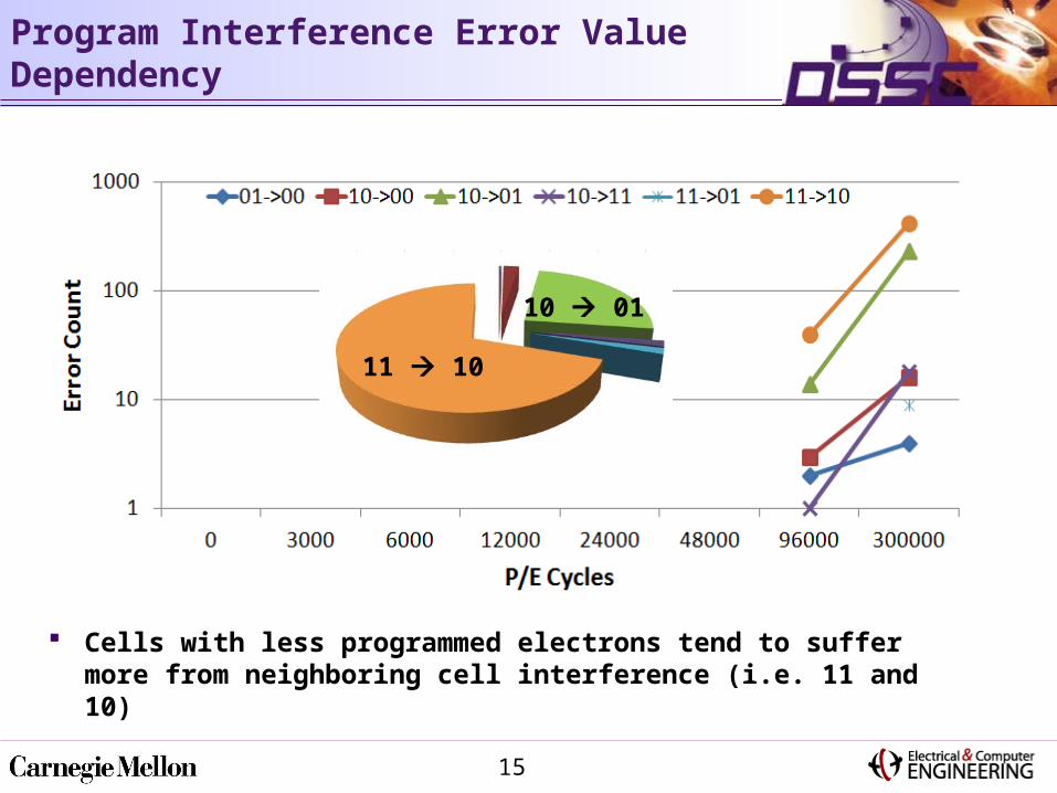
11 10
10 01
Program Interference Error Value Dependency
Cells with less programmed electrons tend to suffer more from neighboring cell interference (i.e. 11 and 10)

16
Program Interference Error Location Dependency
Program interference errors appear in even-MSB pages BER of bottom pages are orders of magnitude higher
17
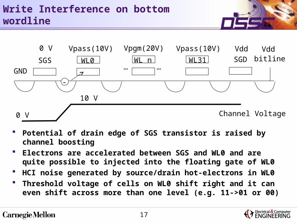
Write Interference on bottom wordline
Potential of drain edge of SGS transistor is raised by channel boosting
Electrons are accelerated between SGS and WL0 and are quite possible to injected into the floating gate of WL0
HCI noise generated by source/drain hot-electrons in WL0 Threshold voltage of cells on WL0 shift right and it can even
shift across more than one level (e.g. 11->01 or 00)
SGS WL0 WL31 SGD…
GND
10 V
0 V
-
0 V Vpass(10V)
WL n…
Vpgm(20V) Vpass(10V) VddbitlineVdd
Channel Voltage

18
Read Error Analysis
11 10 01 00VT
REF1 REF2 REF3
Erased Fully programmed
FloatingGate

19
Erase Errors Analysis
n+ n+
0 V
+18 V
Continuous erases can significantly reduce errors remove residual electrons

20
Conclusions & Future work
Flash errors could show up for any operations Erase error, program error, retention error and read error
Retention errors are the most dominant errors
Flash errors show explainable error patterns Cycle-dependency, value-dependency and location-dependency
Understanding of modern flash memory error patterns will enable designing effective error tolerance mechanisms Value-asymmetry aware coding techniques Cell location-aware wear leveling mechanisms