Embed Size (px)
Citation preview
+
William Stallings
Computer Organization
and Architecture
9th Edition
+ Chapter 2
Computer Evolution and Performance
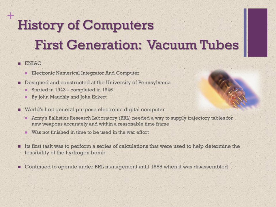
+History of Computers
ENIAC
Electronic Numerical Integrator And Computer
Designed and constructed at the University of Pennsylvania
Started in 1943 – completed in 1946
By John Mauchly and John Eckert
World’s first general purpose electronic digital computer
Army’s Ballistics Research Laboratory (BRL) needed a way to supply trajectory tables for
new weapons accurately and within a reasonable time frame
Was not finished in time to be used in the war effort
Its first task was to perform a series of calculations that were used to help determine the
feasibility of the hydrogen bomb
Continued to operate under BRL management until 1955 when it was disassembled
First Generation: Vacuum Tubes
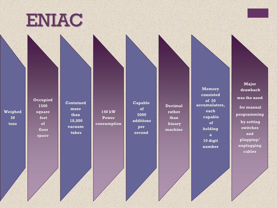
ENIAC
Weighed
30
tons
Occupied
1500
square
feet
of
floor
space
Contained
more
than
18,000
vacuum
tubes
140 kW
Power
consumption
Capable
of
5000
additions
per
second
Decimal
rather
than
binary
machine
Memory
consisted
of 20 accumulators,
each
capable
of
holding
a
10 digit
number
Major
drawback
was the need
for manual
programming
by setting
switches
and
plugging/
unplugging
cables
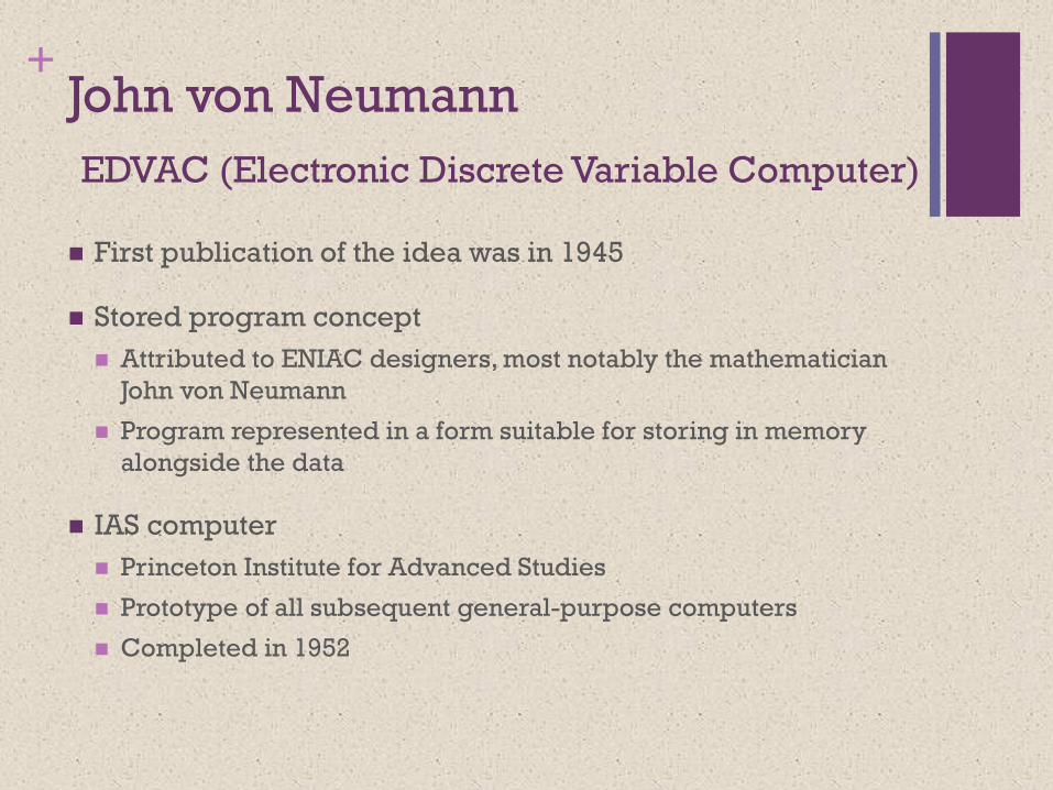
+John von Neumann
First publication of the idea was in 1945
Stored program concept
Attributed to ENIAC designers, most notably the mathematician
John von Neumann
Program represented in a form suitable for storing in memory
alongside the data
IAS computer
Princeton Institute for Advanced Studies
Prototype of all subsequent general-purpose computers
Completed in 1952
EDVAC (Electronic Discrete Variable Computer)
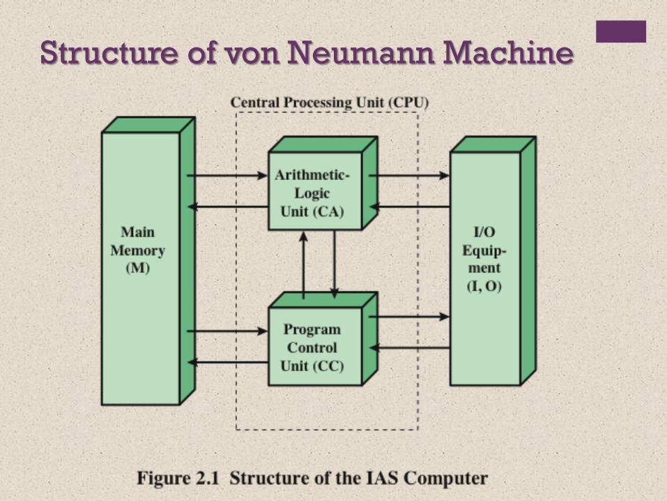
Structure of von Neumann Machine
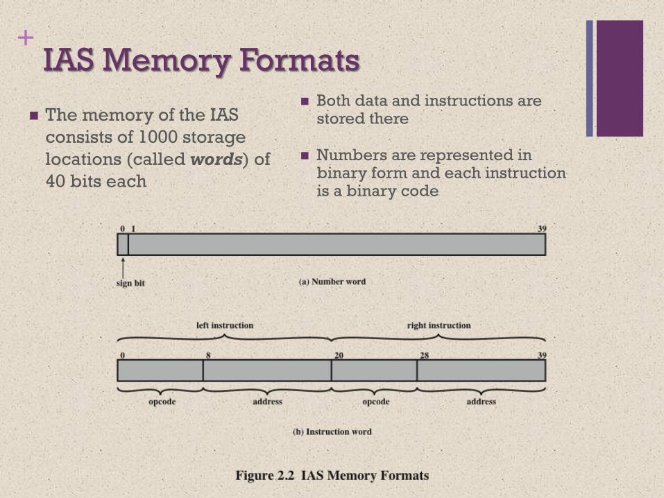
+IAS Memory Formats
Both data and instructions are stored there
Numbers are represented in binary form and each instruction is a binary code
The memory of the IAS
consists of 1000 storage
locations (called words) of
40 bits each
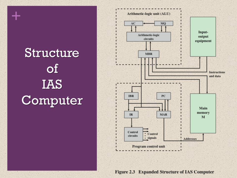
+
Structure
of
IAS
Computer
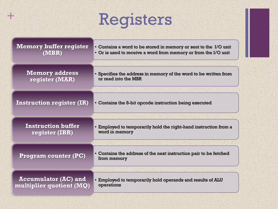
+ Registers
• Contains a word to be stored in memory or sent to the I/O unit
• Or is used to receive a word from memory or from the I/O unit
Memory buffer register (MBR)
• Specifies the address in memory of the word to be written from or read into the MBR
Memory address register (MAR)
• Contains the 8-bit opcode instruction being executedInstruction register (IR)
• Employed to temporarily hold the right-hand instruction from a word in memory
Instruction buffer register (IBR)
• Contains the address of the next instruction pair to be fetched from memoryProgram counter (PC)
• Employed to temporarily hold operands and results of ALU operations
Accumulator (AC) and multiplier quotient (MQ)
+Commercial Computers
1947 – Eckert and Mauchly formed the Eckert-Mauchly Computer Corporation to manufacture computers commercially
UNIVAC I (Universal Automatic Computer)
First successful commercial computer
Was intended for both scientific and commercial applications
Commissioned by the US Bureau of Census for 1950 calculations
The Eckert-Mauchly Computer Corporation became part of the UNIVAC division of the Sperry-Rand Corporation
UNIVAC II – delivered in the late 1950’s
Had greater memory capacity and higher performance
Backward compatible
UNIVAC
+
IBM
Was the major manufacturer of punched-card processing equipment
Delivered its first electronic stored-program computer (701) in 1953
Intended primarily for scientific applications
Introduced 702 product in 1955
Hardware features made it
suitable to business
applications
Series of 700/7000 computers established IBM as the overwhelmingly dominant computer manufacturer
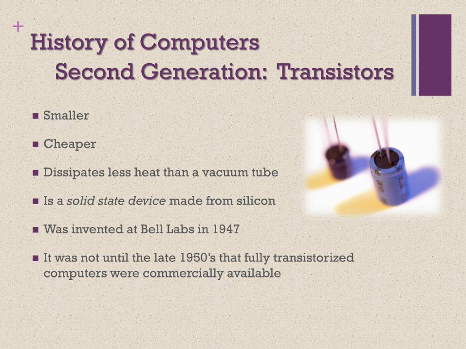
+History of Computers
Smaller
Cheaper
Dissipates less heat than a vacuum tube
Is a solid state device made from silicon
Was invented at Bell Labs in 1947
It was not until the late 1950’s that fully transistorized
computers were commercially available
Second Generation: Transistors
+
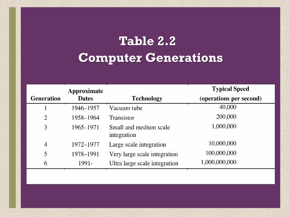
Computer Generations
Table 2.2
Computer Generations
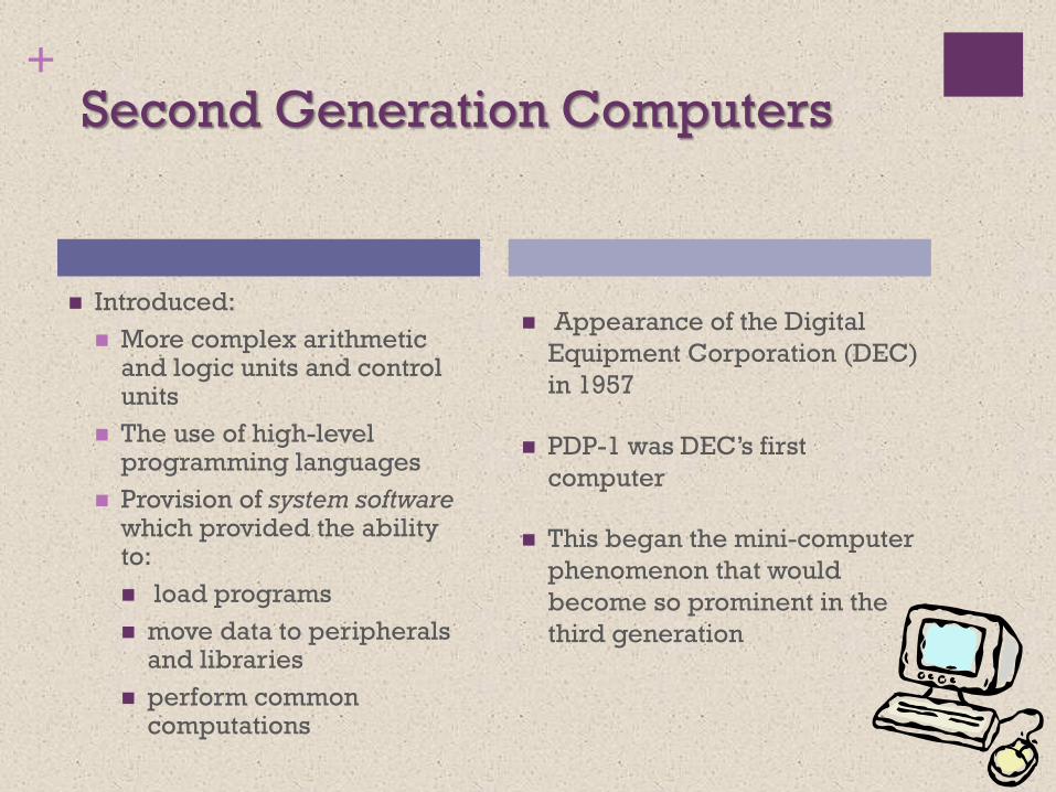
+Second Generation Computers
Introduced:
More complex arithmetic and logic units and control units
The use of high-level programming languages
Provision of system software which provided the ability to:
load programs
move data to peripherals and libraries
perform common computations
Appearance of the Digital
Equipment Corporation (DEC)
in 1957
PDP-1 was DEC’s first
computer
This began the mini-computer
phenomenon that would
become so prominent in the
third generation
Third Generation: Integrated Circuits
History of Computers
1958 – the invention of the integrated circuit
Discrete component
Single, self-contained transistor
Manufactured separately, packaged in their own containers, and
soldered or wired together onto masonite-like circuit boards
Manufacturing process was expensive and cumbersome
The two most important members of the third generation
were the IBM System/360 and the DEC PDP-8
+Microelectronics
+Integrated
Circuits
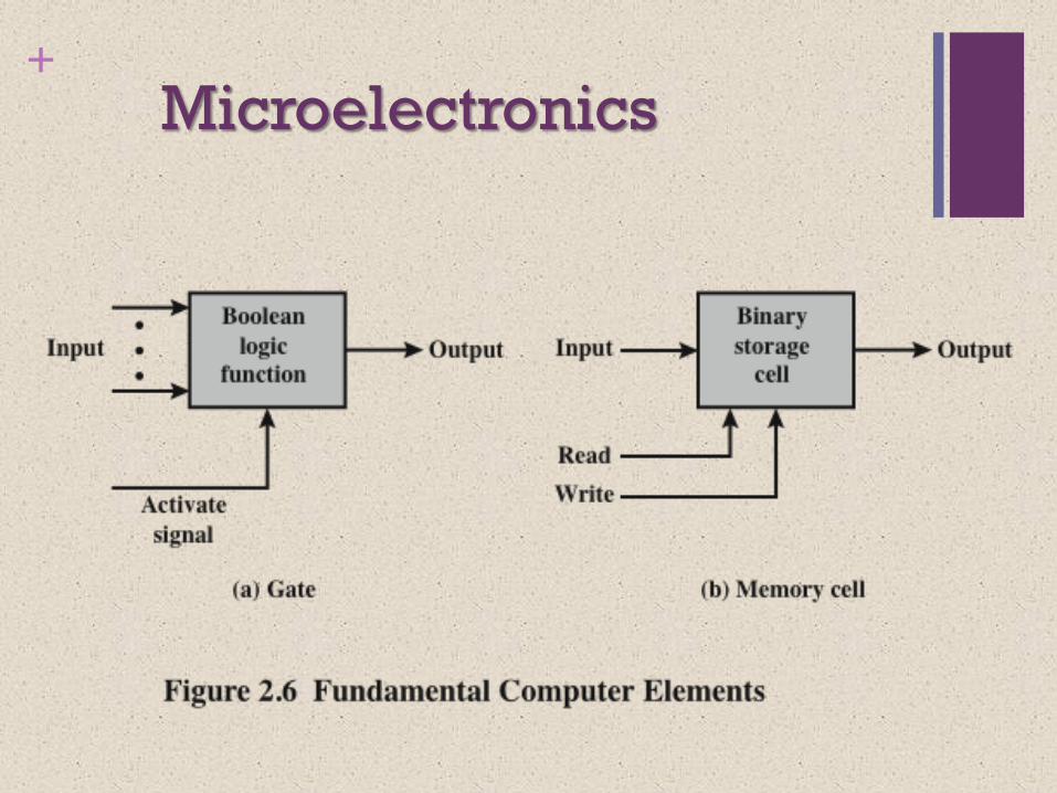
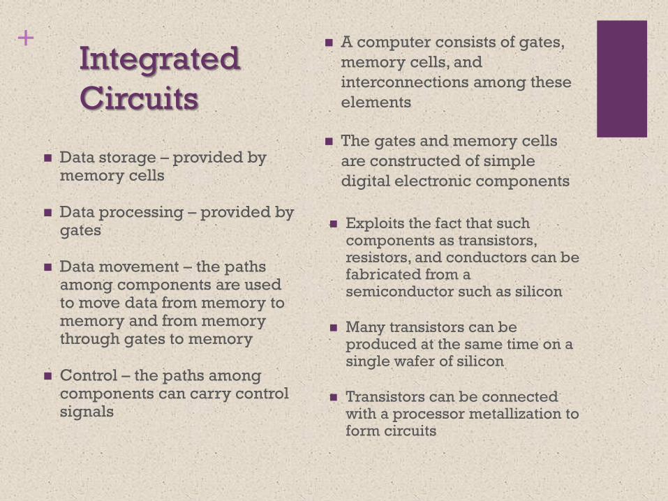
A computer consists of gates,
memory cells, and
interconnections among these
elements
The gates and memory cells
are constructed of simple
digital electronic components
Data storage – provided by memory cells
Data processing – provided by gates
Data movement – the paths among components are used to move data from memory to memory and from memory through gates to memory
Control – the paths among components can carry control signals
Exploits the fact that such components as transistors, resistors, and conductors can be fabricated from a semiconductor such as silicon
Many transistors can be produced at the same time on a single wafer of silicon
Transistors can be connected with a processor metallization to form circuits
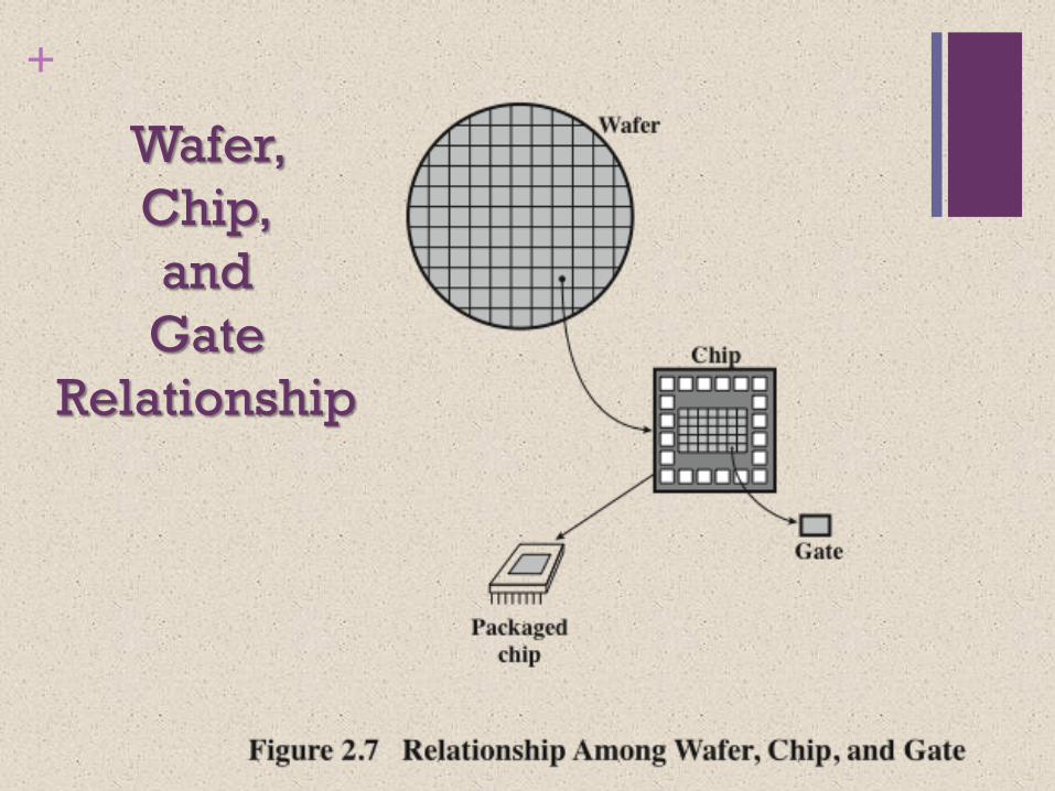
+
Wafer,
Chip,
and
Gate
Relationship
+
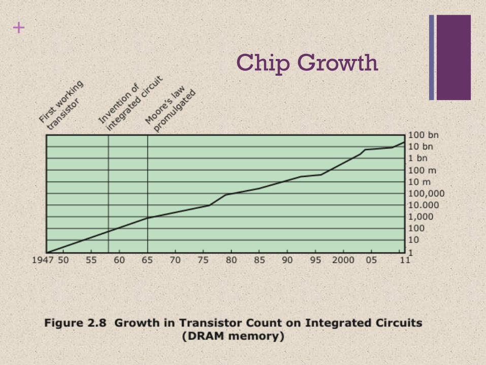
Chip Growth
Moore’s Law
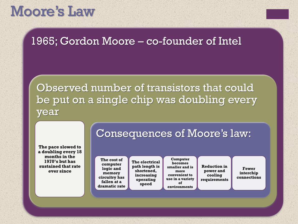
1965; Gordon Moore – co-founder of Intel
Observed number of transistors that could be put on a single chip was doubling every year
The pace slowed to a doubling every 18
months in the 1970’s but has
sustained that rate ever since
Consequences of Moore’s law:
The cost of computer logic and memory
circuitry has fallen at a
dramatic rate
The electrical path length is
shortened, increasing operating
speed
Computer becomes
smaller and is more
convenient to use in a variety
of environments
Reduction in power and
cooling requirements
Fewer interchip
connections
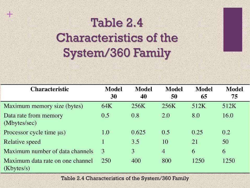
+Table 2.4
Characteristics of the
System/360 Family
Table 2.4 Characteristics of the System/360 Family
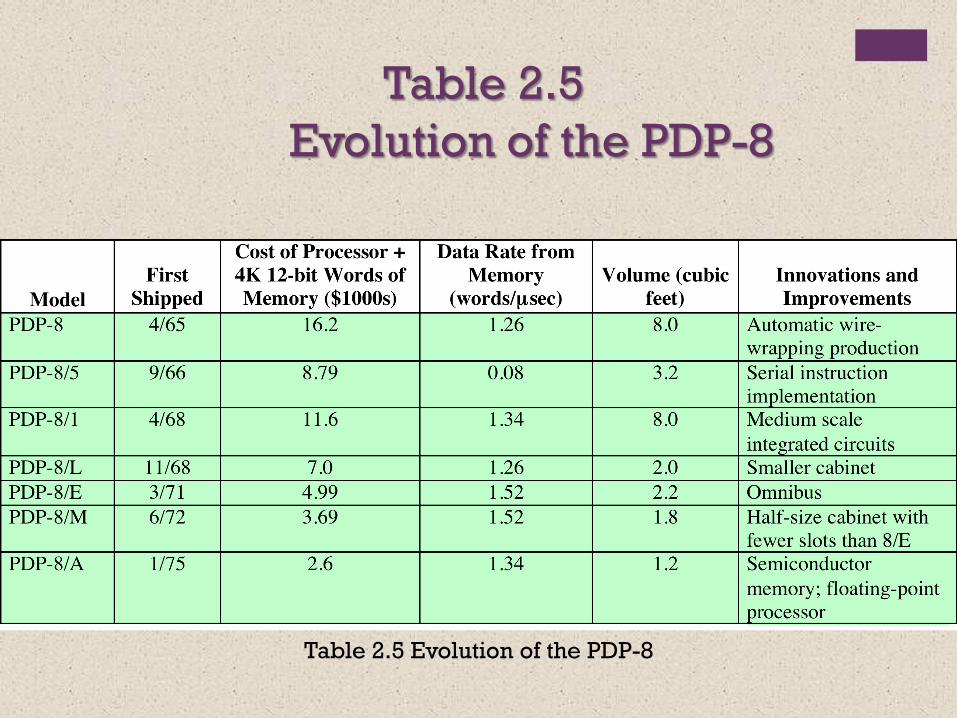
Table 2.5
Evolution of the PDP-8
Table 2.5 Evolution of the PDP-8
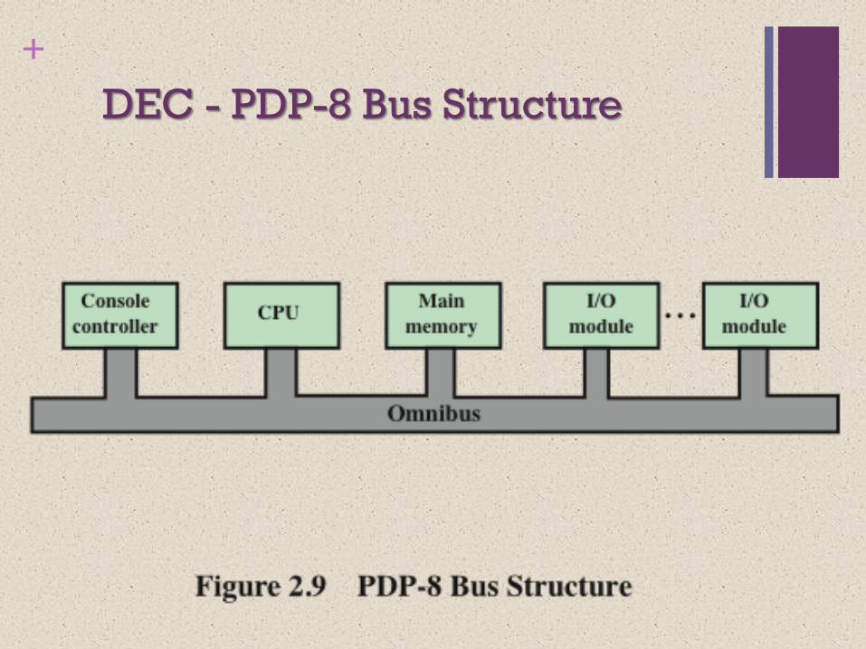
+
DEC - PDP-8 Bus Structure
+
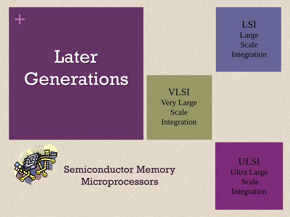
Later
Generations
LSILarge
Scale
Integration
VLSIVery Large
Scale
Integration
ULSIUltra Large
Scale
Integration
Semiconductor Memory
Microprocessors
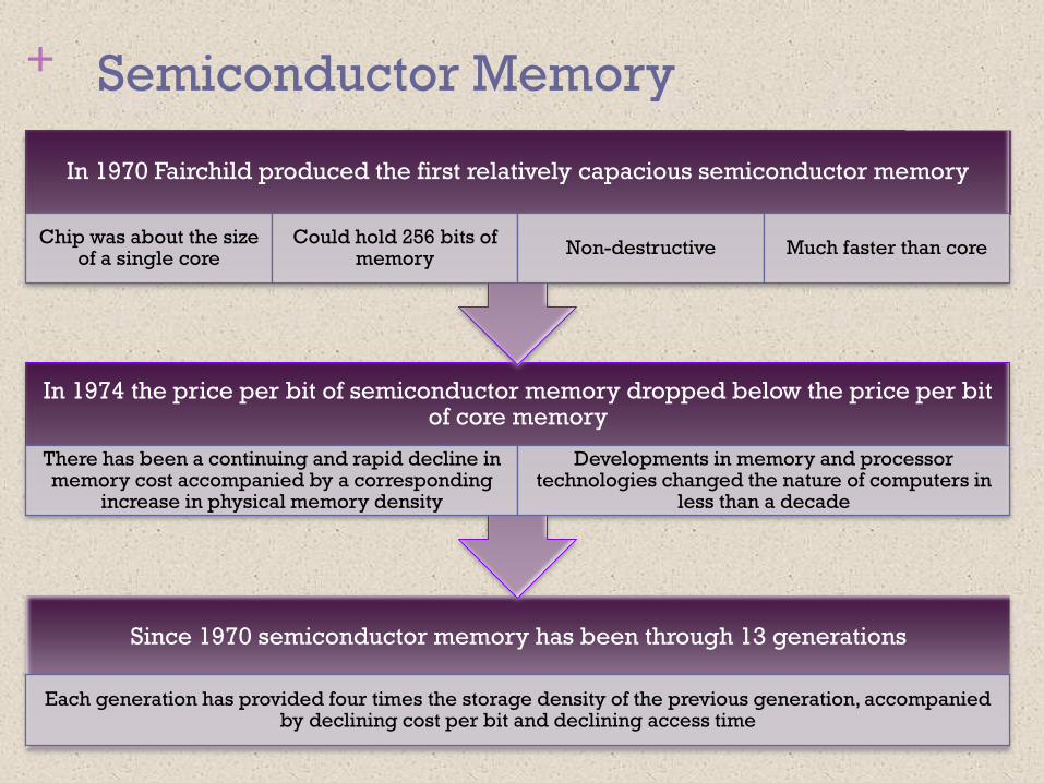
+ Semiconductor Memory
Since 1970 semiconductor memory has been through 13 generations
Each generation has provided four times the storage density of the previous generation, accompanied by declining cost per bit and declining access time
In 1974 the price per bit of semiconductor memory dropped below the price per bit of core memory
There has been a continuing and rapid decline in memory cost accompanied by a corresponding
increase in physical memory density
Developments in memory and processor technologies changed the nature of computers in
less than a decade
In 1970 Fairchild produced the first relatively capacious semiconductor memory
Chip was about the size of a single core
Could hold 256 bits of memory
Non-destructive Much faster than core
+Microprocessors
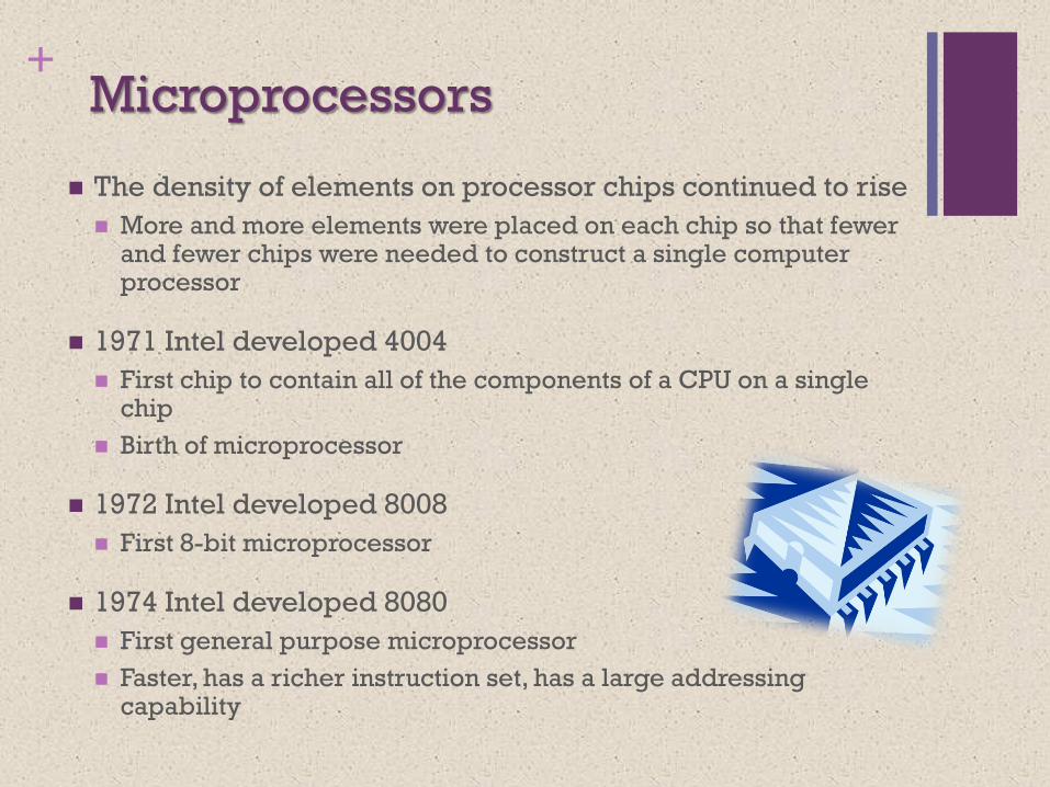
The density of elements on processor chips continued to rise
More and more elements were placed on each chip so that fewer and fewer chips were needed to construct a single computer processor
1971 Intel developed 4004
First chip to contain all of the components of a CPU on a single chip
Birth of microprocessor
1972 Intel developed 8008
First 8-bit microprocessor
1974 Intel developed 8080
First general purpose microprocessor
Faster, has a richer instruction set, has a large addressing capability
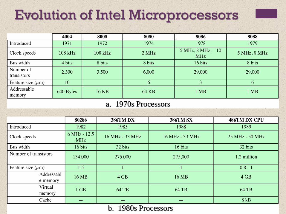
Evolution of Intel Microprocessors
a. 1970s Processors
b. 1980s Processors
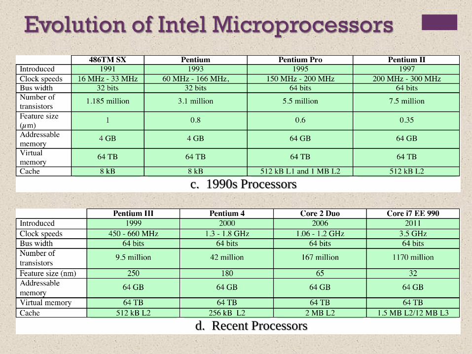
Evolution of Intel Microprocessors
c. 1990s Processors
d. Recent Processors
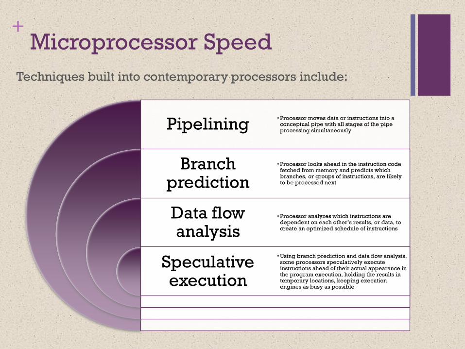
+Microprocessor Speed
Pipelining
Branch prediction
Data flow analysis
Speculative execution
• Processor moves data or instructions into a conceptual pipe with all stages of the pipe processing simultaneously
• Processor looks ahead in the instruction code fetched from memory and predicts which branches, or groups of instructions, are likely to be processed next
• Processor analyzes which instructions are dependent on each other’s results, or data, to create an optimized schedule of instructions
• Using branch prediction and data flow analysis, some processors speculatively execute instructions ahead of their actual appearance in the program execution, holding the results in temporary locations, keeping execution engines as busy as possible
Techniques built into contemporary processors include:
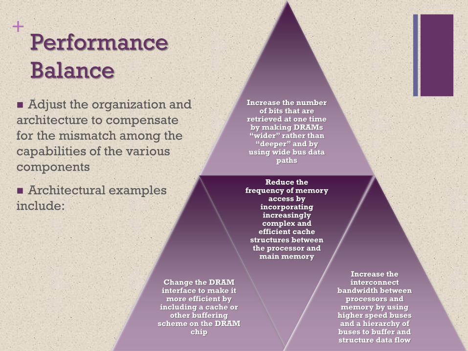
+Performance
Balance
Increase the number of bits that are
retrieved at one time by making DRAMs “wider” rather than
“deeper” and by using wide bus data
paths
Change the DRAM interface to make it
more efficient by including a cache or
other buffering scheme on the DRAM
chip
Reduce the frequency of memory
access by incorporating increasingly complex and
efficient cache structures between the processor and
main memory
Increase the interconnect
bandwidth between processors and
memory by using higher speed buses and a hierarchy of buses to buffer and structure data flow
Adjust the organization and
architecture to compensate
for the mismatch among the
capabilities of the various
components
Architectural examples
include:
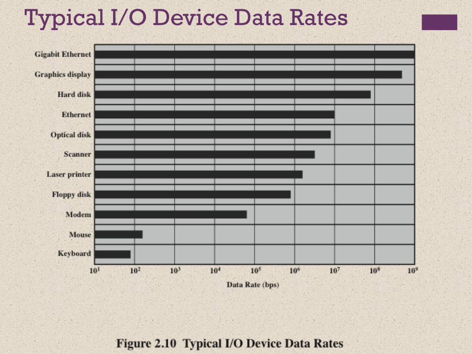
Typical I/O Device Data Rates
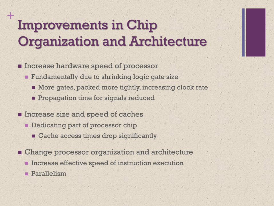
+Improvements in Chip
Organization and Architecture
Increase hardware speed of processor
Fundamentally due to shrinking logic gate size
More gates, packed more tightly, increasing clock rate
Propagation time for signals reduced
Increase size and speed of caches
Dedicating part of processor chip
Cache access times drop significantly
Change processor organization and architecture
Increase effective speed of instruction execution
Parallelism
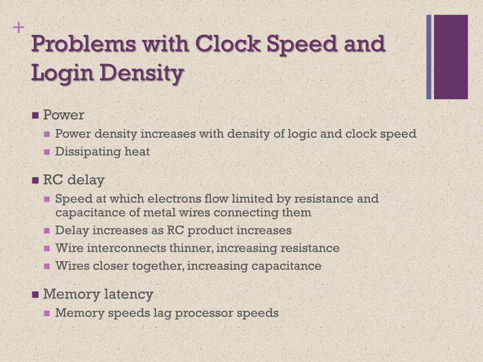
+Problems with Clock Speed and
Login Density
Power
Power density increases with density of logic and clock speed
Dissipating heat
RC delay
Speed at which electrons flow limited by resistance and capacitance of metal wires connecting them
Delay increases as RC product increases
Wire interconnects thinner, increasing resistance
Wires closer together, increasing capacitance
Memory latency
Memory speeds lag processor speeds
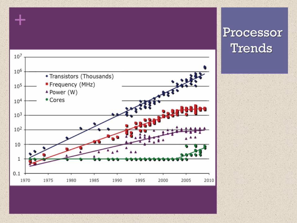
+Processor
Trends
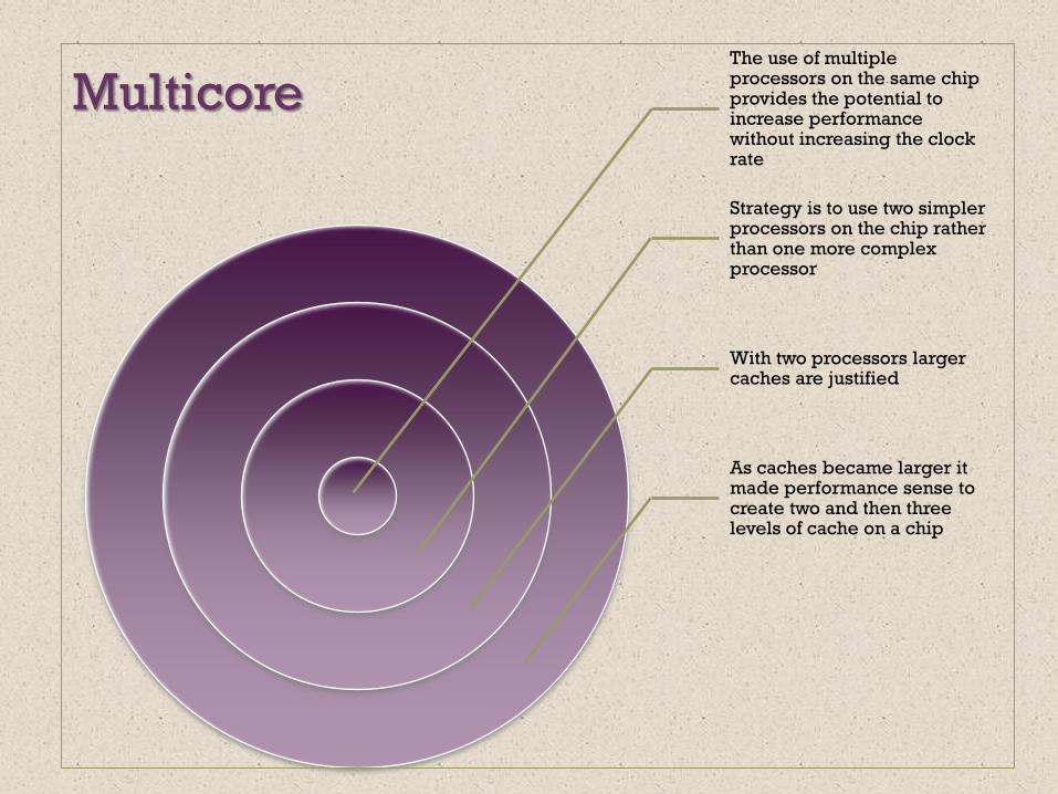
The use of multiple processors on the same chip provides the potential to increase performance without increasing the clock rate
Strategy is to use two simpler processors on the chip rather than one more complex processor
With two processors larger caches are justified
As caches became larger it made performance sense to create two and then three levels of cache on a chip
Multicore
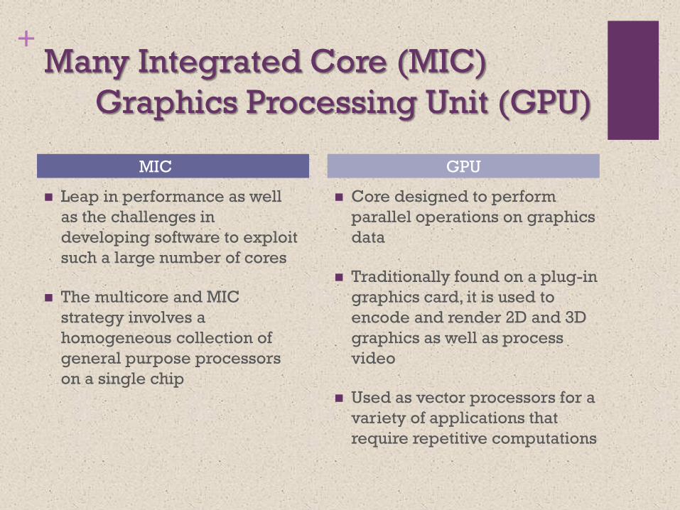
+Many Integrated Core (MIC)
Graphics Processing Unit (GPU)
Leap in performance as well
as the challenges in
developing software to exploit
such a large number of cores
The multicore and MIC
strategy involves a
homogeneous collection of
general purpose processors
on a single chip
Core designed to perform
parallel operations on graphics
data
Traditionally found on a plug-in
graphics card, it is used to
encode and render 2D and 3D
graphics as well as process
video
Used as vector processors for a
variety of applications that
require repetitive computations
MIC GPU
+
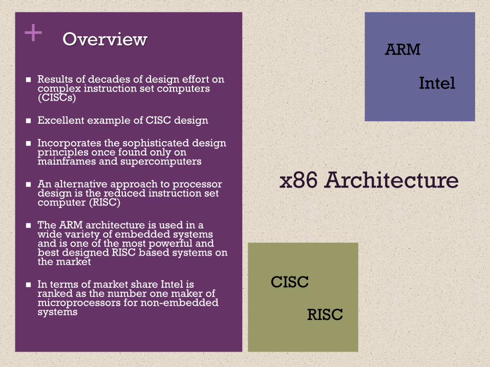
x86 Architecture
Results of decades of design effort on complex instruction set computers (CISCs)
Excellent example of CISC design
Incorporates the sophisticated design principles once found only on mainframes and supercomputers
An alternative approach to processor design is the reduced instruction set computer (RISC)
The ARM architecture is used in a wide variety of embedded systems and is one of the most powerful and best designed RISC based systems on the market
In terms of market share Intel is ranked as the number one maker of microprocessors for non-embedded systems
Overview
CISC
RISC
Intel
ARM
+
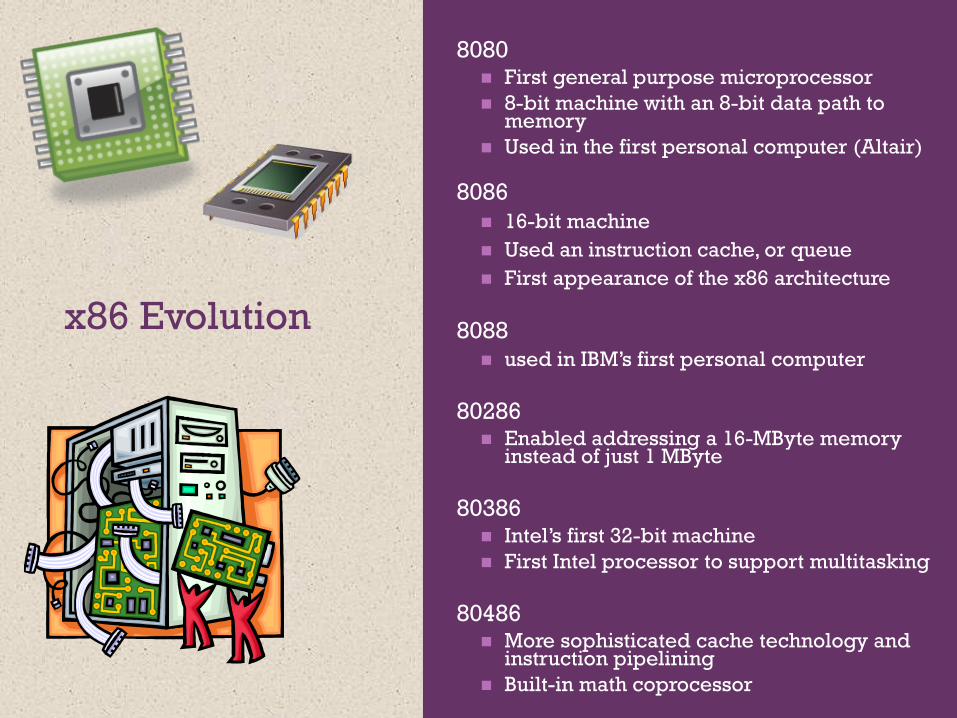
x86 Evolution
8080 First general purpose microprocessor
8-bit machine with an 8-bit data path to memory
Used in the first personal computer (Altair)
8086
16-bit machine
Used an instruction cache, or queue
First appearance of the x86 architecture
8088
used in IBM’s first personal computer
80286 Enabled addressing a 16-MByte memory
instead of just 1 MByte
80386 Intel’s first 32-bit machine
First Intel processor to support multitasking
80486 More sophisticated cache technology and
instruction pipelining
Built-in math coprocessor
+
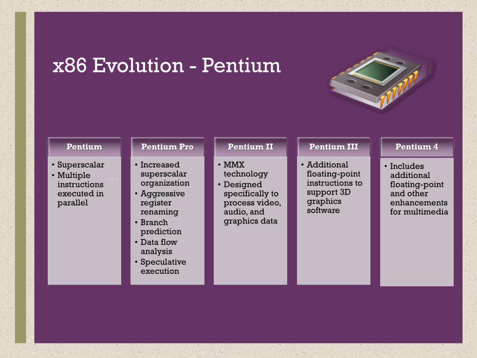
x86 Evolution - Pentium
Pentium
• Superscalar
• Multiple instructions executed in parallel
Pentium Pro
• Increased superscalar organization
• Aggressive register renaming
• Branch prediction
• Data flow analysis
• Speculative execution
Pentium II
• MMX technology
• Designed specifically to process video, audio, and graphics data
Pentium III
• Additional floating-point instructions to support 3D graphics software
Pentium 4
• Includes additional floating-point and other enhancements for multimedia
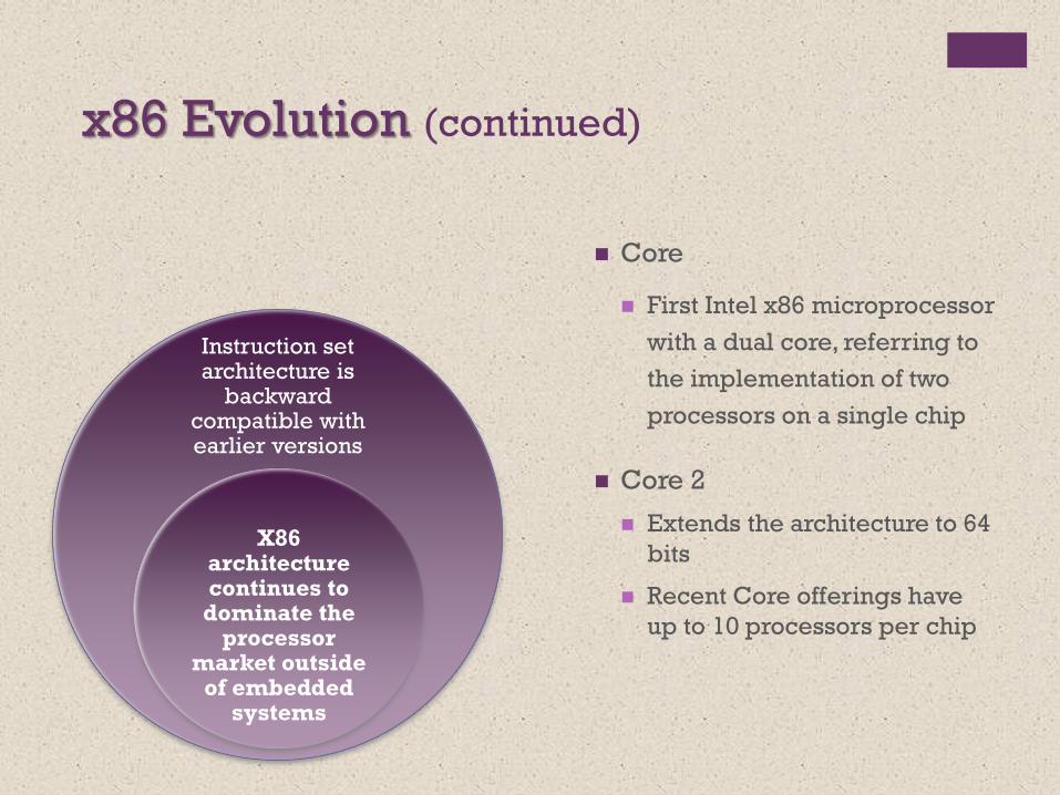
x86 Evolution (continued)
Core
First Intel x86 microprocessor
with a dual core, referring to
the implementation of two
processors on a single chip
Core 2
Extends the architecture to 64
bits
Recent Core offerings have
up to 10 processors per chip
Instruction set architecture is
backward compatible with earlier versions
X86 architecture continues to dominate the
processor market outside
of embedded systems


![Comboni Vincenzo v Shankar's Emporium (Pte) Ltd [2007] 2 SLR 1020](https://img.pdfslide.us/doc/110x75/5515ddbc497959111e8b4ffa/comboni-vincenzo-v-shankars-emporium-pte-ltd-2007-2-slr-1020.jpg)